JP4940468B2 - Slip ring - Google Patents
Slip ring Download PDFInfo
- Publication number
- JP4940468B2 JP4940468B2 JP2006312852A JP2006312852A JP4940468B2 JP 4940468 B2 JP4940468 B2 JP 4940468B2 JP 2006312852 A JP2006312852 A JP 2006312852A JP 2006312852 A JP2006312852 A JP 2006312852A JP 4940468 B2 JP4940468 B2 JP 4940468B2
- Authority
- JP
- Japan
- Prior art keywords
- signal
- ring
- shield
- brush
- brushes
- Prior art date
- Legal status (The legal status is an assumption and is not a legal conclusion. Google has not performed a legal analysis and makes no representation as to the accuracy of the status listed.)
- Active
Links
Images
Landscapes
- Details Of Connecting Devices For Male And Female Coupling (AREA)
Description
本発明は、スリップリングに関し、特に、信号リングの両側にシールドリングを積層させ、信号リングに摺接する信号用ブラシの両側にシールド用ブラシを配設し、信号リング及び信号用ブラシに対するシールド効果を高め、外部からのノイズの混入を防止するための新規な改良に関する。 The present invention relates to a slip ring, and in particular, a shield ring is laminated on both sides of a signal ring, and a shield brush is disposed on both sides of a signal brush that is in sliding contact with the signal ring. The present invention relates to a novel improvement for preventing noise contamination from the outside.
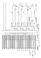
一般に、画像等の信号の送受には、特許文献等を特に示していないが、図3で示す積層型の構成が採用されている。
図3において、符号1で示されるものは、複数のシールドリング2と信号リング3と絶縁板4とを、軸方向に沿って積層させてなるスリップリング用のリング体であり、このリング体1の前記シールドリング2と信号リング3とは前記絶縁板4を介して互いに絶縁されている。
In general, for the transmission and reception of signals such as images, a patent document or the like is not particularly shown, but a stacked configuration shown in FIG. 3 is adopted.
In FIG. 3, what is indicated by reference numeral 1 is a ring body for slip rings in which a plurality of
前記リング体1の近傍には、シールド用ブラシ5と信号用ブラシ6とを交互に配設したブラシホルダ7が配設され、前記各シールド用ブラシ5は前記各シールドリング2に摺接し、前記各信号用ブラシ6は前記各信号リング3に摺接している。
In the vicinity of the ring body 1, a brush holder 7 in which
前記各シールド用ブラシ5に接続されたシールド用接続線8は、シールド線9の外皮であるシールド部10の端面11の一端11aに接続され、前記信号用ブラシ6には、前記シールド線9のシールド部10に覆われた信号線12が接続されている。
前記各シールド線9の出力側9aは図示しない受信回路側へ接続されている。
The
The
前述の構成で、リング体1が回転し、このリング体1に設けてある、例えば、回転磁気ヘッド又は電子回路等からの出力信号は、前記信号リング3、信号用ブラシ6及び信号線12を介して外部へ出力される。
また、外部からの電源等の外部信号は、前記信号線12、信号用ブラシ6及び信号リング3を介して前記電子回路等へ入力されるために送信される。
In the above-described configuration, the ring body 1 rotates, and an output signal provided on the ring body 1, for example, from a rotating magnetic head or an electronic circuit, passes through the signal ring 3, the
An external signal such as an external power supply is transmitted for input to the electronic circuit or the like via the
従来のスリップリングは、以上のように構成されていたため、次のような課題が存在していた。
すなわち、信号リングと信号用ブラシの一方側のみにしかシールドリングが設けられていないため、信号リング及び信号用ブラシに対するシールド効果が十分ではなく、外部ノイズが混入しやすく、信号のS/N比が低下していた。
また、インピーダンスマッチングがとりにくい状況となっていた。
Since the conventional slip ring is configured as described above, the following problems exist.
That is, since the shield ring is provided only on one side of the signal ring and the signal brush, the shielding effect for the signal ring and the signal brush is not sufficient, and external noise is likely to be mixed, and the signal S / N ratio is increased. Had fallen.
In addition, impedance matching is difficult.
本発明によるスリップリングは、絶縁板を用いて信号リングとシールドリングを積層させ、多層型に形成したリング体と、前記各信号リング及びシールドリングに摺接する複数の信号用ブラシ及びシールド用ブラシとを有するブラシホルダと、前記信号用ブラシに接続された信号線と、前記シールド用ブラシに接続され前記信号線を覆うためのシールド部を有するシールド線とを備え、回転する前記信号リングと前記信号用ブラシとの間で信号の送受を行うようにしたスリップリングにおいて、前記信号用リングの両側にはシールドリングが設けられ、前記信号用ブラシの両側には前記シールド用ブラシが配設され、前記信号リングの両側に前記絶縁板を介して設けられた前記各シールドリングには、前記信号リングの外径より大径のオーバーハング部が形成され、前記オーバーハング部の凹部内に前記絶縁板が配設されている構成であり、また、前記各シールド用ブラシは、筒状の前記シールド線の端面の両端にシールド用接続線を介して接続されている構成である。 A slip ring according to the present invention includes a ring body formed by laminating a signal ring and a shield ring using an insulating plate, and a plurality of signal brushes and shield brushes that are in sliding contact with the signal rings and the shield ring. The signal ring connected to the signal brush, and the shield wire connected to the shield brush and having a shield part for covering the signal line, the rotating signal ring and the signal In the slip ring that transmits and receives signals to and from the signal brush, shield rings are provided on both sides of the signal ring, and the shield brush is disposed on both sides of the signal brush , the each shield ring provided through the insulating plate on both sides of the front SL signal rings, large diameter over than the outer diameter of the signal ring Hang portion is formed, the insulating plate Ri configuration der is arranged, also, before Symbol brush each shield before Symbol the recess of the overhang portion, both ends of the end surface of the cylindrical of the shield wire Are connected via a shield connecting line.
本発明によるスリップリングは、以上のように構成されているため、次のような効果を得ることができる。
すなわち、信号リングと信号用ブラシの両側に、シールドリングとシールド用ブラシが配設されているため、信号リングと信号用ブラシに対するシールド効果を十分に得ることができ、信号線を通る信号への外部雑音を遮断することができる。
また、各シールドリングに、信号リングの外径より大径のオーバーハング部が設けられているため、信号リング及び信号用部ブラシに対するシールド効果をより一層高めることができる。
Since the slip ring according to the present invention is configured as described above, the following effects can be obtained.
That is, since the shield ring and the shield brush are disposed on both sides of the signal ring and the signal brush, a sufficient shielding effect for the signal ring and the signal brush can be obtained, and the signal passing through the signal line can be obtained. External noise can be blocked.
Further, since each shield ring is provided with an overhang portion having a diameter larger than the outer diameter of the signal ring, the shielding effect for the signal ring and the signal portion brush can be further enhanced.
本発明は、信号リングの両側にシールドリングを積層させ、信号リングに摺接する信号用ブラシの両側にシールド用ブラシを配設し、信号リング及び信号用ブラシに対するシールド効果を高め、外部からのノイズの混入を防止するようにしたスリップリングを提供することを目的とする。 In the present invention, the shield ring is laminated on both sides of the signal ring, and the shield brush is disposed on both sides of the signal brush that is in sliding contact with the signal ring to enhance the shielding effect on the signal ring and the signal brush, and noise from the outside. It is an object of the present invention to provide a slip ring that prevents contamination of the material.
以下、図面と共に本発明によるスリップリングの好適な実施の形態について説明する。 尚、従来例と同一又は同等部分には、同一符号を付して説明する。
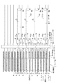
図1において符号1で示されるものは、複数のシールドリング2と信号リング3と絶縁板4とを、軸方向に沿って積層させてなるスリップリング用のリング体であり、このリング体1の前記各シールドリング2と信号リング3とは前記各絶縁板4を介して互いに絶縁されている。
すなわち、このリング体1は、1個の信号リング3の両側に各々絶縁板4を介して一対のシールドリング2が積層され、この構成の繰り返し構造(多層型)によって所定数の信号リング3が積層されている。
Hereinafter, preferred embodiments of a slip ring according to the present invention will be described with reference to the drawings. In addition, the same code | symbol is attached | subjected and demonstrated to a part the same as that of a prior art example, or an equivalent part.
What is denoted by reference numeral 1 in FIG. 1 is a ring body for slip rings in which a plurality of
That is, in this ring body 1, a pair of
前記リング体1の近傍には、互いに独立した複数の信号用ブラシ6と、この各信号用ブラシ6の両側に配設された一対のシールド用ブラシ5とを有するブラシホルダ7が配設され、前記各シールド用ブラシ5は前記各シールドリング2に摺接し、前記各信号用ブラシ6は前記各信号リング3に摺接している。
A brush holder 7 having a plurality of
前記各シールド用ブラシ5に接続されたシールド用接続線8は、シールド線9の外皮であるシールド部10の端面11の両端11aに接続され、前記各信号用ブラシ6には、前記シールド線9のシールド部10に覆われた信号線12が接続されている。
前記各シールド線9の出力側9aは図示しない受信回路側へ接続されている。
The
The
前述の構成で、リング体1が回転し、このリング体1に設けてある、例えば、回転磁気ヘッド又は電子回路等からの出力信号は、前記各信号リング3、信号用ブラシ6及び信号線12を介して外部へ出力される。
また、外部からの電源等の外部信号は、前記信号線12、信号用ブラシ6及び信号リング3を介して前記電子回路等へ入力すなわち送信される。
In the above-described configuration, the ring body 1 is rotated, and output signals from, for example, a rotating magnetic head or an electronic circuit provided on the ring body 1 are sent to the signal rings 3, the
An external signal such as an external power supply is input, that is, transmitted to the electronic circuit or the like via the
また、前記各信号リング3は一対のシールドリング2によって挟持されていると共に、前記信号用ブラシ6は一対のシールド用ブラシ5によって挟持されているため、信号リング3及び信号用ブラシ6に対するシールド効果が従来よりも大幅に高く、前記シールド線9を経た出力信号及びリング体1側の電子回路等に対する入力信号のS/N比を向上させることができる。
Further, since each signal ring 3 is sandwiched between a pair of
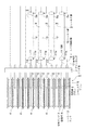
次に、図2は、本発明の他の形態を示す構成で、図1と同一又は同等部分には同一符号を付して説明を省略し、異なる部分についてのみ説明する。
すなわち、前記各シールドリング2の前記各信号リング3側には、前記信号リング3の外径よりも大径のオーバーハング部30が設けられており、このオーバーハング部30の凹部31内に前記絶縁板4が収まる状態で配設されている。
Next, FIG. 2 is a structure which shows the other form of this invention, attaches | subjects the same code | symbol to the part which is the same as that of FIG. 1, or an equivalent, and abbreviate | omits description and demonstrates only a different part.
That is, an overhang portion 30 having a diameter larger than the outer diameter of the signal ring 3 is provided on the signal ring 3 side of each
前記各オーバーハング部30は、前記各信号リング3及び信号用ブラシ6を挟持し、かつ、各信号リング3を覆っていることにより、シールド効果が高く、外部からの電気的なノイズが信号リング3及び信号用ブラシ6を介して入出力信号に混入することを防止するように構成されている。
Each overhang portion 30 sandwiches each signal ring 3 and
1 リング体
2 シールドリング
3 信号リング
4 絶縁板
5 シールド用ブラシ
6 信号用ブラシ
7 ブラシホルダ
8 シールド用接続線
9 シールド線
10 シールド部
11 端面
12 信号線
DESCRIPTION OF SYMBOLS 1
Claims (2)
回転する前記信号リング(3)と前記信号用ブラシ(6)との間で信号の送受を行うようにしたスリップリングにおいて、
前記信号用リング(3)の両側にはシールドリング(2)が設けられ、前記信号用ブラシ(6)の両側には前記シールド用ブラシ(5)が配設され、前記信号リング(3)の両側に前記絶縁板(4)を介して設けられた前記各シールドリング(2)には、前記信号リング(3)の外径より大径のオーバーハング部(30)が形成され、前記オーバーハング部(30)の凹部(31)内に前記絶縁板(4)が配設されていることを特徴とするスリップリング。 The signal ring (3) and the shield ring (2) are laminated using an insulating plate (4), and the ring body (1) formed in a multilayer type is slid onto the signal ring (3) and the shield ring (2). A brush holder (7) having a plurality of signal brushes (6) and a shield brush (5) in contact, a signal line (12) connected to the signal brush (6), and the shield brush (5 ) And a shield wire (9) having a shield part (10) for covering the signal line (12),
In the slip ring adapted to send and receive signals between the rotating signal ring (3) and the signal brush (6),
The shield ring (2) is provided on both sides of the signal ring (3), brush the shield on both sides of the signal brush (6) (5) is arranged, prior SL signal ring (3) the each shield ring provided through the insulating plate on either side of (4) (2), the diameter of the overhang portion than the outer diameter of the signal ring (3) (30) is formed, before Symbol features and be away rippling said insulating plate in the recess (31) of the overhang portion (30) (4) is arranged.
Priority Applications (1)
| Application Number | Priority Date | Filing Date | Title |
|---|---|---|---|
| JP2006312852A JP4940468B2 (en) | 2006-11-20 | 2006-11-20 | Slip ring |
Applications Claiming Priority (1)
| Application Number | Priority Date | Filing Date | Title |
|---|---|---|---|
| JP2006312852A JP4940468B2 (en) | 2006-11-20 | 2006-11-20 | Slip ring |
Publications (2)
| Publication Number | Publication Date |
|---|---|
| JP2008130319A JP2008130319A (en) | 2008-06-05 |
| JP4940468B2 true JP4940468B2 (en) | 2012-05-30 |
Family
ID=39555954
Family Applications (1)
| Application Number | Title | Priority Date | Filing Date |
|---|---|---|---|
| JP2006312852A Active JP4940468B2 (en) | 2006-11-20 | 2006-11-20 | Slip ring |
Country Status (1)
| Country | Link |
|---|---|
| JP (1) | JP4940468B2 (en) |
Families Citing this family (5)
| Publication number | Priority date | Publication date | Assignee | Title |
|---|---|---|---|---|
| JP2012099376A (en) * | 2010-11-04 | 2012-05-24 | Nidec Servo Corp | Slip ring device |
| JP6253558B2 (en) * | 2014-09-25 | 2017-12-27 | 株式会社東芝 | Slip ring device |
| US9735530B2 (en) * | 2015-03-10 | 2017-08-15 | General Electric Company | Apparatus and method for axially spacing conductive rings of a slip ring assembly |
| DE202020101851U1 (en) | 2020-04-03 | 2021-07-12 | Walter Kraus Gmbh | Rotary transmitter for high frequency signals |
| JP7271780B1 (en) | 2022-12-26 | 2023-05-11 | ソフトバンク株式会社 | rotating connector |
Family Cites Families (3)
| Publication number | Priority date | Publication date | Assignee | Title |
|---|---|---|---|---|
| JPS6488485A (en) * | 1987-09-29 | 1989-04-03 | Ricoh Kk | Image forming device |
| JP3587156B2 (en) * | 1999-10-18 | 2004-11-10 | 松下電工株式会社 | Field emission type electron source and method of manufacturing the same |
| JP2001189183A (en) * | 2000-01-06 | 2001-07-10 | Ricoh Co Ltd | Current collector |
-
2006
- 2006-11-20 JP JP2006312852A patent/JP4940468B2/en active Active
Also Published As
| Publication number | Publication date |
|---|---|
| JP2008130319A (en) | 2008-06-05 |
Similar Documents
| Publication | Publication Date | Title |
|---|---|---|
| JP2013243668A5 (en) | ||
| JP5752936B2 (en) | Transmission line applied to non-contact slip ring | |
| JP4940468B2 (en) | Slip ring | |
| JP2007535112A5 (en) | ||
| JP2006504380A5 (en) | ||
| WO2014080963A4 (en) | Printed wiring board and printed circuit board | |
| KR20080073480A (en) | Flat Cables and Electronic Devices Having the Same | |
| JP2010527136A (en) | High frequency drum type slip ring module | |
| JP2009290454A5 (en) | ||
| JP6074749B2 (en) | Coil parts and their mounting boards | |
| CN103124037A (en) | Strong and weak current isolation conductive slip ring | |
| JP2016066946A (en) | Signal transmission cable | |
| JP5604083B2 (en) | Power semiconductor module with control function and built-in transmitter | |
| JP2017513203A (en) | Wiring member | |
| CN107924869B (en) | Semiconductor device and method for manufacturing the same | |
| TW200710893A (en) | Multilayer capacitor | |
| US10027062B2 (en) | Signal transmission cable | |
| JP2009193760A (en) | Composite cable, motor control device including the same, and robot | |
| KR102023772B1 (en) | electronic device of lamination structure based on through poles | |
| JP4562781B2 (en) | Data communication device | |
| JP4203005B2 (en) | Common mode choke coil | |
| TWI476787B (en) | Device suppressing common-mode radiation | |
| KR20120096432A (en) | Flexible flat cable for low voltage differential signaling | |
| WO2009114399A3 (en) | Multiple electrode connector having coaxial cables | |
| JP6631441B2 (en) | Wiring structure and image forming apparatus |
Legal Events
| Date | Code | Title | Description |
|---|---|---|---|
| A621 | Written request for application examination |
Free format text: JAPANESE INTERMEDIATE CODE: A621 Effective date: 20091119 |
|
| A977 | Report on retrieval |
Free format text: JAPANESE INTERMEDIATE CODE: A971007 Effective date: 20110726 |
|
| A131 | Notification of reasons for refusal |
Free format text: JAPANESE INTERMEDIATE CODE: A131 Effective date: 20110802 |
|
| A521 | Request for written amendment filed |
Free format text: JAPANESE INTERMEDIATE CODE: A523 Effective date: 20110929 |
|
| TRDD | Decision of grant or rejection written | ||
| A01 | Written decision to grant a patent or to grant a registration (utility model) |
Free format text: JAPANESE INTERMEDIATE CODE: A01 Effective date: 20120207 |
|
| A01 | Written decision to grant a patent or to grant a registration (utility model) |
Free format text: JAPANESE INTERMEDIATE CODE: A01 |
|
| A61 | First payment of annual fees (during grant procedure) |
Free format text: JAPANESE INTERMEDIATE CODE: A61 Effective date: 20120209 |
|
| R150 | Certificate of patent or registration of utility model |
Ref document number: 4940468 Country of ref document: JP Free format text: JAPANESE INTERMEDIATE CODE: R150 Free format text: JAPANESE INTERMEDIATE CODE: R150 |
|
| FPAY | Renewal fee payment (event date is renewal date of database) |
Free format text: PAYMENT UNTIL: 20150309 Year of fee payment: 3 |
|
| R250 | Receipt of annual fees |
Free format text: JAPANESE INTERMEDIATE CODE: R250 |
|
| R250 | Receipt of annual fees |
Free format text: JAPANESE INTERMEDIATE CODE: R250 |
|
| R250 | Receipt of annual fees |
Free format text: JAPANESE INTERMEDIATE CODE: R250 |
|
| R250 | Receipt of annual fees |
Free format text: JAPANESE INTERMEDIATE CODE: R250 |
|
| R250 | Receipt of annual fees |
Free format text: JAPANESE INTERMEDIATE CODE: R250 |
|
| R250 | Receipt of annual fees |
Free format text: JAPANESE INTERMEDIATE CODE: R250 |
|
| R250 | Receipt of annual fees |
Free format text: JAPANESE INTERMEDIATE CODE: R250 |
|
| R250 | Receipt of annual fees |
Free format text: JAPANESE INTERMEDIATE CODE: R250 |
|
| R250 | Receipt of annual fees |
Free format text: JAPANESE INTERMEDIATE CODE: R250 |
|
| R250 | Receipt of annual fees |
Free format text: JAPANESE INTERMEDIATE CODE: R250 |
|
| R250 | Receipt of annual fees |
Free format text: JAPANESE INTERMEDIATE CODE: R250 |
|
| R250 | Receipt of annual fees |
Free format text: JAPANESE INTERMEDIATE CODE: R250 |