JP4939076B2 - Charged particle beam writing method - Google Patents
Charged particle beam writing method Download PDFInfo
- Publication number
- JP4939076B2 JP4939076B2 JP2006043498A JP2006043498A JP4939076B2 JP 4939076 B2 JP4939076 B2 JP 4939076B2 JP 2006043498 A JP2006043498 A JP 2006043498A JP 2006043498 A JP2006043498 A JP 2006043498A JP 4939076 B2 JP4939076 B2 JP 4939076B2
- Authority
- JP
- Japan
- Prior art keywords
- stage
- sample
- charged particle
- speed
- magnetic field
- Prior art date
- Legal status (The legal status is an assumption and is not a legal conclusion. Google has not performed a legal analysis and makes no representation as to the accuracy of the status listed.)
- Expired - Fee Related
Links
Images


Description
本発明は、荷電粒子ビーム描画方法に係り、例えば、荷電粒子ビームを可変成形させながら試料に荷電粒子ビームを照射する描画方法に関する。 The present invention relates to a charged particle beam writing method, for example, a writing method for irradiating a sample with a charged particle beam while variably shaping the charged particle beam.
半導体デバイスの微細化の進展を担うリソグラフィ技術は半導体製造プロセスのなかでも唯一パターンを生成する極めて重要なプロセスである。近年、LSIの高集積化に伴い、半導体デバイスに要求される回路線幅は年々微細化されてきている。これらの半導体デバイスへ所望の回路パターンを形成するためには、高精度の原画パターン(レチクル或いはマスクともいう。)が必要となる。ここで、電子線(電子ビーム)描画技術は本質的に優れた解像性を有しており、高精度の原画パターンの生産に用いられる。 Lithography technology, which is responsible for the progress of miniaturization of semiconductor devices, is an extremely important process for generating a pattern among semiconductor manufacturing processes. In recent years, with the high integration of LSI, circuit line widths required for semiconductor devices have been reduced year by year. In order to form a desired circuit pattern on these semiconductor devices, a highly accurate original pattern (also referred to as a reticle or a mask) is required. Here, the electron beam (electron beam) drawing technique has an essentially excellent resolution, and is used for producing a high-precision original pattern.
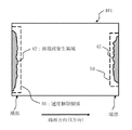
図9は、従来の可変成形型電子線描画装置の動作を説明するための概念図である。
可変成形型電子線描画装置(EB(Electron beam)描画装置)における第1のアパーチャ410には、電子線330を成形するための矩形例えば長方形の開口411が形成されている。また、第2のアパーチャ420には、第1のアパーチャ410の開口411を通過した電子線330を所望の矩形形状に成形するための可変成形開口421が形成されている。荷電粒子ソース430から照射され、第1のアパーチャ410の開口411を通過した電子線330は、偏向器により偏向され、第2のアパーチャ420の可変成形開口421の一部を通過して、所定の一方向(例えば、X方向とする)に連続的に移動するステージ上に搭載された試料340に照射される。すなわち、第1のアパーチャ410の開口411と第2のアパーチャ420の可変成形開口421との両方を通過できる矩形形状が、X方向に連続的に移動するステージ上に搭載された試料340の描画領域に描画される。第1のアパーチャ410の開口411と第2のアパーチャ420の可変成形開口421との両方を通過させ、任意形状を作成する方式を可変成形方式という。
FIG. 9 is a conceptual diagram for explaining the operation of a conventional variable shaping type electron beam drawing apparatus.
In a first aperture 410 in a variable shaping type electron beam drawing apparatus (EB (Electron beam) drawing apparatus), a rectangular, for example, rectangular opening 411 for forming the electron beam 330 is formed. Further, the second aperture 420 is formed with a variable shaping opening 421 for shaping the electron beam 330 having passed through the opening 411 of the first aperture 410 into a desired rectangular shape. The electron beam 330 irradiated from the charged particle source 430 and passed through the opening 411 of the first aperture 410 is deflected by the deflector, passes through a part of the variable shaping opening 421 of the second aperture 420, and passes through a predetermined range. The
ここで、上述したステージ上に搭載された試料340に電子ビームが照射される際に、対物レンズにより焦点が調整される。かかる対物レンズの磁場の一部が、ステージ上に漏れている場合、ステージ上の導電性部品内に渦電流が生じる。かかる渦電流によりステージ上に磁場が発生し、描画位置に誤差が生じてしまう。かかる渦電流に関する電磁力学について、文献に記載がされている(例えば、非特許文献1参照)。
上述したように、対物レンズの磁場の一部が、ステージ上に漏れている場合、ステージ上の導電性部品内に生じる渦電流によりステージ上に磁場が発生し、ビームの描画位置のずれによる誤差が生じてしまうといった問題があった。 As described above, when a part of the magnetic field of the objective lens leaks on the stage, the magnetic field is generated on the stage due to the eddy current generated in the conductive parts on the stage, and the error due to the deviation of the drawing position of the beam. There was a problem that would occur.
そこで、本発明は、かかる問題点を克服し、ビームの描画位置のずれを低減する描画方法を提供することを目的とする。 Therefore, an object of the present invention is to provide a drawing method that overcomes such problems and reduces the deviation of the drawing position of the beam.
本発明の一態様の荷電粒子ビーム描画方法は、
試料が載置されたステージを連続移動させながら荷電粒子ビームを用いて試料に描画する荷電粒子ビーム描画方法において、
一方向に描画してパターンの誤差寸法を測定し、次に、前記一方向逆向きに描画してまたパターンの誤差寸法を測定し、前記一方向の誤差寸法と前記一方向逆向きの誤差寸法の差分を演算して渦電流による磁場が生じる領域を特定し、
特定された渦電流による磁場が生じる領域を、前記磁場により生じる誤差寸法に反比例した速度以下になるように低下させた前記ステージの移動速度で描画することを特徴とする。
The charged particle beam drawing method of one embodiment of the present invention includes:
In a charged particle beam drawing method for drawing on a sample using a charged particle beam while continuously moving the stage on which the sample is placed,
Draw in one direction to measure the error dimension of the pattern, then draw in the one-way reverse direction and measure the error dimension of the pattern again, the one-way error dimension and the one-way reverse error dimension The region where the magnetic field due to the eddy current occurs is calculated by calculating the difference between
A region where a magnetic field due to the specified eddy current is generated is drawn at a moving speed of the stage which is lowered so as to be equal to or less than a speed inversely proportional to an error size generated by the magnetic field.
後述するように、渦電流による磁場はステージの移動速度に比例する。よって、かかる領域の速度を下げることで磁場の磁束密度(強度)を弱めることができる。磁場を弱めることで、照射される荷電粒子ビームが磁場から受ける影響を小さくすることができる。 As will be described later, the magnetic field generated by the eddy current is proportional to the moving speed of the stage. Therefore, the magnetic flux density (intensity) of the magnetic field can be weakened by reducing the speed of the region. By weakening the magnetic field, the influence of the irradiated charged particle beam from the magnetic field can be reduced.
ここで、かかるステージの移動速度は、磁場により生じる誤差寸法に反比例した速度以下になるように低下させると好適である。 Here, it is preferable that the moving speed of the stage is lowered so as to be equal to or lower than the speed inversely proportional to the error size caused by the magnetic field.
位置ずれ量は、荷電粒子ビームが磁場から受ける影響(磁場の磁束密度)に比例する。よって、位置ずれ量は、ステージの移動速度に比例する。したがって、ステージの移動速度を誤差寸法に反比例した速度以下に設定することで、磁場から受ける影響を排除することができる。 The amount of misalignment is proportional to the influence of the charged particle beam on the magnetic field (magnetic flux density of the magnetic field). Therefore, the amount of positional deviation is proportional to the moving speed of the stage. Accordingly, the influence of the magnetic field can be eliminated by setting the moving speed of the stage to a speed that is inversely proportional to the error dimension.
そして、低下させるステージの移動速度は、磁場が生じない場合のステージの移動速度に、許容誤差寸法を磁場により生じる誤差寸法で除した値を乗じた速度以下になるように設定すると好適である。 The stage moving speed to be lowered is preferably set to be equal to or lower than the speed obtained by multiplying the stage moving speed when no magnetic field is generated by the value obtained by dividing the allowable error dimension by the error dimension generated by the magnetic field.
本発明の他の態様の荷電粒子ビーム描画方法は、
試料が載置されたステージを一定速度で連続移動させながら荷電粒子ビームを用いて試料に描画する荷電粒子ビーム描画方法において、
試料の描画領域の端部を一定速度で描画する場合のステージの移動速度を描画領域の中央部を一定速度で描画する場合の移動速度より遅くすることを特徴とする。
A charged particle beam writing method according to another aspect of the present invention includes:
In a charged particle beam drawing method for drawing on a sample using a charged particle beam while continuously moving the stage on which the sample is placed at a constant speed,
The stage moving speed when the edge of the drawing area of the sample is drawn at a constant speed is made slower than the moving speed when the center of the drawing area is drawn at a constant speed.
後述するように、渦電流による磁場が生じる領域は、描画領域の端部に集中していることを発明者は見出した。そこで、描画領域の端部を一定速度で描画する場合のステージの移動速度を描画領域の中央部を一定速度で描画する場合の移動速度より遅くすることで、かかる渦電流による磁場の影響を排除することができる。 As will be described later, the inventor has found that the region where the magnetic field due to the eddy current is generated is concentrated at the end of the drawing region. Therefore, the influence of the magnetic field due to the eddy current is eliminated by making the stage moving speed when drawing the edge of the drawing area at a constant speed slower than the moving speed when drawing the center part of the drawing area at a constant speed. can do.
本発明の他の態様の荷電粒子ビーム描画方法は、
試料が載置されたステージをパターン密度に応じて可変速で連続移動させながら荷電粒子ビームを用いて試料に描画する荷電粒子ビーム描画方法において、
試料の描画領域の端部を描画する場合のステージの移動速度を、描画領域の中央部における同等のパターン密度の領域におけるステージの移動速度より遅くすることを特徴とする。
A charged particle beam writing method according to another aspect of the present invention includes:
In a charged particle beam writing method for drawing on a sample using a charged particle beam while continuously moving the stage on which the sample is mounted at a variable speed according to the pattern density,
The stage moving speed when drawing the end of the drawing area of the sample is made slower than the moving speed of the stage in an area having the same pattern density in the center of the drawing area.
可変速でステージを連続移動させる場合には、パターン密度によってステージの移動速度が設定される。そこで、渦電流による磁場が生じる描画領域の端部を描画する場合には、端部を描画する場合のステージの移動速度を描画領域の中央部における同等のパターン密度の領域におけるステージの移動速度より遅くすることで、かかる渦電流による磁場の影響を排除することができる。 When the stage is continuously moved at a variable speed, the moving speed of the stage is set depending on the pattern density. Therefore, when drawing the edge of the drawing area where a magnetic field due to eddy current is drawn, the stage moving speed when drawing the edge is higher than the stage moving speed in the area of the equivalent pattern density in the center of the drawing area. By slowing down, the influence of the magnetic field due to the eddy current can be eliminated.
本発明によれば、渦電流による磁場の影響を排除することができるので、ビームの描画位置のずれを低減することができる。 According to the present invention, since the influence of the magnetic field due to the eddy current can be eliminated, it is possible to reduce the deviation of the drawing position of the beam.
以下、実施の形態では、荷電粒子ビームの一例として、電子ビームを用いた構成について説明する。但し、荷電粒子ビームは、電子ビームに限るものではなく、イオンビーム等の他の荷電粒子を用いたビームでも構わない。 Hereinafter, in the embodiment, a configuration using an electron beam will be described as an example of a charged particle beam. However, the charged particle beam is not limited to an electron beam, and may be a beam using other charged particles such as an ion beam.
実施の形態1.
図1は、実施の形態1における描画装置の構成を示す概念図である。
図1において、荷電粒子ビーム描画装置の一例である描画装置100は、照射部の一例となる描画部150を構成する電子鏡筒102、描画室103、XYステージ105、電子銃201、照明レンズ202、第1のアパーチャ203、投影レンズ204、偏向器205、第2のアパーチャ206、対物レンズ207、偏向器208、支持ピン222、台座312、反射ミラー314、参照ミラー216、支柱332、駆動部106を備え、制御部160として、描画制御回路110、偏向制御部の一例となる偏向制御回路112、ステージ駆動回路114、CPU120、メモリ122、レーザー干渉計132、レーザー干渉計134を備えている。コンピュータとなるCPU120には、描画制御回路110、偏向制御回路112、ステージ駆動回路114、メモリ122、レーザー干渉計132、レーザー干渉計134が図示していないバスを介して接続されている。描画制御回路110、偏向制御回路112、ステージ駆動回路114は、CPU120から出力される制御信号により制御される。また、CPU120で演算される入力データ或いは出力データ等はメモリ122に記憶される。そして、CPU120内には、微分演算部124といった機能を有している。
Embodiment 1 FIG.
FIG. 1 is a conceptual diagram illustrating a configuration of a drawing apparatus according to the first embodiment.
In FIG. 1, a drawing apparatus 100, which is an example of a charged particle beam drawing apparatus, includes an electron column 102, a drawing chamber 103, an
そして、電子鏡筒102内には、電子銃201、照明レンズ202、第1のアパーチャ203、投影レンズ204、偏向器205、第2のアパーチャ206、対物レンズ207、偏向器208が配置されている。描画室103内には、XYステージ105、台座312、反射ミラー314、参照ミラー216、支持ピン222、支柱332が配置されている。図1では、本実施の形態1を説明する上で必要な構成部分以外については記載を省略している。描画装置100にとって、通常、必要なその他の構成が含まれることは言うまでもない。
In the electron barrel 102, an electron gun 201, an illumination lens 202, a first aperture 203, a projection lens 204, a deflector 205, a second aperture 206, an objective lens 207, and a deflector 208 are arranged. . In the drawing chamber 103, an
また、図1では、コンピュータとなるCPU120で、微分演算部124といった機能の処理を実行するように記載しているがこれに限るものではなく、電気的な回路によるハードウェアにより実施させても構わない。或いは、電気的な回路によるハードウェアとソフトウェアとの組み合わせにより実施させても構わない。或いは、かかるハードウェアとファームウェアとの組み合わせでも構わない。
In FIG. 1, the
電子銃201から出た荷電粒子ビームの一例となる電子ビーム200は、照明レンズ202により矩形例えば長方形の穴を持つ第1のアパーチャ203全体を照明する。ここで、電子ビーム200をまず矩形例えば長方形に成形する。そして、第1のアパーチャ203を通過した第1のアパーチャ像の電子ビーム200は、投影レンズ204により第2のアパーチャ206上に投影される。かかる第2のアパーチャ206上での第1のアパーチャ像の位置は、描画制御回路110により制御された偏向器205によって偏向制御され、ビーム形状と寸法を変化させることができる。そして、第2のアパーチャ206を通過した第2のアパーチャ像の電子ビーム200は、対物レンズ207により焦点を合わせ、偏向制御回路112に制御された偏向器208により偏向され、ステージ駆動回路114に制御された駆動部106により連続移動するXYステージ105上の試料101の所望する位置に照射される。
An electron beam 200 as an example of a charged particle beam emitted from the electron gun 201 illuminates the entire first aperture 203 having a rectangular hole, for example, a rectangular hole by an illumination lens 202. Here, the electron beam 200 is first formed into a rectangle, for example, a rectangle. Then, the electron beam 200 of the first aperture image that has passed through the first aperture 203 is projected onto the second aperture 206 by the projection lens 204. The position of the first aperture image on the second aperture 206 is deflection-controlled by the deflector 205 controlled by the
図2は、実施の形態1におけるステージ移動の様子を説明するための図である。
試料101に描画する場合には、XYステージ105を例えばX方向に連続移動させながら、描画(露光)面を電子ビーム200が偏向可能な短冊状の複数のストライプ領域に仮想分割された試料101の1つのストライプ領域上を電子ビーム200が照射する。XYステージ105のX方向の移動は、連続移動とし、同時に電子ビーム200のショット位置もステージ移動に追従させる。連続移動させることで描画時間を短縮させることができる。そして、1つのストライプ領域を描画し終わったら、XYステージ105をY方向にステップ送りしてX方向(今度は逆向き)に次のストライプ領域の描画動作を行なう。各ストライプ領域の描画動作を蛇行させるように進めることでXYステージ105の移動時間を短縮することができる。
FIG. 2 is a diagram for explaining the stage movement in the first embodiment.
In the case of drawing on the
図3は、実施の形態1におけるステージ速度分布の一例を示す図である。
図3では、XYステージ105が一定速度で連続移動しながら電子ビーム200を用いて試料101に描画する電子ビーム描画方法を示している。渦電流による磁場はステージの移動速度に比例する。よって、図3に示すように、試料101の描画領域上における渦電流発生領域を描画する際のXYステージ105の移動速度を下げることで磁場の磁束密度(強度)を弱めることができる。磁場を弱めることで、照射される電子ビームが磁場から受ける影響を小さくすることができる。
FIG. 3 is a diagram showing an example of the stage speed distribution in the first embodiment.
FIG. 3 shows an electron beam writing method in which the
図4は、実施の形態1における渦電流の発生メカニズムについて説明するための概念図である。
描画装置100内では、対物レンズ207等の電子レンズの磁場10の一部がXYステージ105上に漏れている場合、XYステージ105上の導電性部品に渦電流(eddy current)20が生じる。ここで、渦電流密度をJ、材質等で決まる電気伝導率をσ、形状等の境界条件によって決まる電場をE、ステージ速度をv、対物レンズからの磁場(磁束密度)をBとすると、渦電流密度Jは、以下の式(式1)にて表すことができる。
式1:J=σ(E+v×B)
FIG. 4 is a conceptual diagram for explaining the generation mechanism of the eddy current in the first embodiment.
In the drawing apparatus 100, when a part of the magnetic field 10 of the electron lens such as the objective lens 207 leaks onto the
Formula 1: J = σ (E + v × B)
ここで、渦電流密度Jを位置(x,y,z)で偏微分すると、以下の式(式2)のように表すことができる。
式2:divJ=∂Jx/∂x+∂Jy/∂y+∂Jz/∂z=0
Here, when the eddy current density J is partially differentiated at the position (x, y, z), it can be expressed as the following equation (Equation 2).
Equation 2: divJ = ∂J x / ∂x + ∂J y / ∂y + ∂J z / ∂z = 0
式2は、0以外では発散してしまうので、値「0」をとることになる。よって、式1を微分した場合には、以下の式(式3)のように表すことができる。
式3:divJ=σdivE+σdiv(v×B)=0
Since Expression 2 diverges except for 0, the value “0” is taken. Therefore, when Formula 1 is differentiated, it can be expressed as the following Formula (Formula 3).
Formula 3: divJ = σdivE + σdiv (v × B) = 0
よって、div(v×B)=−divEとなり、Eはvに比例する(E∝v)ことがわかる。また、(v×B)もvに比例する{(v×B)∝v}ことになるので、(E+v×B)もvに比例する{(E+v×B)∝v}ことになる。よって、渦電流密度Jは、ステージ速度vに比例する(J∝v)ことになる。 Therefore, div (v × B) = − divE, and E is proportional to v (E 比例 v). Since (v × B) is also {(v × B) ∝v} proportional to v, (E + v × B) is also {(E + v × B) ∝v} proportional to v. Therefore, the eddy current density J is proportional to the stage speed v (J∝v).
図5は、実施の形態1における渦電流によるステージ上の磁場の様子を示す概念図である。
図5に示すように、XYステージ105上に渦電流20が発生すると、かかる渦電流20による磁場30がXYステージ105上に発生する。そして、かかる磁場30の磁束密度をB’とすると、式1における磁場10の磁束密度Bを磁場30の磁束密度B’に置き換えた式となり、渦電流密度Jは、磁場30の磁束密度B’に比例する(J∝B’)ので、やはり、磁場30の磁束密度をB’もステージ速度vに比例する(B’∝v)ことになる。照射される電子ビーム200は、磁場30の磁束密度をB’によって曲げられるので、それによって生じるビーム位置のずれ量(誤差寸法x)は、ステージ速度vに比例する(x∝v)ことになる。
FIG. 5 is a conceptual diagram showing the state of the magnetic field on the stage due to the eddy current in the first embodiment.
As shown in FIG. 5, when an
よって、試料101上に渦電流20による磁場30が生じる場合に、渦電流20による磁場30が生じる領域を描画する際のXYステージ105の移動速度を低下させることで、ビーム位置のずれ量(誤差寸法x)をその分、低減させることができる。よって、XYステージ105の移動速度は、磁場30により生じる誤差寸法xに反比例した速度以下になるように低下させると好適である。これにより磁場30から受ける影響を排除することができる。
Therefore, when the
ここで、許容する許容誤差寸法をx’、低下後のXYステージ105の移動速度をv’とすると、x’/x=v’/vの関係が成り立つので、低下後のXYステージ105の移動速度をv’=v・x’/xとなる。よって、かかる移動速度をv’以下でより遅い速度でXYステージ105を移動させれば、磁場30から受ける影響を排除することができる。すなわち、低下させるステージの移動速度v’は、磁場30が生じない場合のステージの移動速度vに、許容誤差寸法x’を磁場30により生じる誤差寸法xで除した値を乗じた速度以下になるように設定すると好適である。
Here, if the allowable error dimension is x ′ and the moving speed of the lowered
図6は、実施の形態1における渦電流による位置ずれ領域を示す図である。
電子ビーム描画において描画したバターンの位置ずれの要因としては、かかる渦電流による位置ずれとそもそもの位置に依存した位置ずれとが考えられる。よって、例えばX方向にXYステージ105を連続移動させながら描画する場合には、まず、X方向(正方向)に描画してパターンの位置ずれ量を測定し、次に、X方向逆向き(負方向)に描画してまたパターンの位置ずれ量を測定する。そして、得られた位置ずれ量の差分をとれば、位置に依存しない位置ずれ量の分布を得ることができる。渦電流による位置ずれは、位置に依存しないため、差分で得られた領域に渦電流による位置ずれ領域が存在することになる。図6では、かかる位置に依存しない位置ずれ量の分布を示している。図6によれば、試料101の描画領域の中央部ではなく、試料101の描画領域の端部(両端部)に位置ずれ領域40が集中していることがわかる。
FIG. 6 is a diagram showing a misalignment region due to eddy current in the first embodiment.
As a cause of the positional deviation of the pattern drawn in the electron beam drawing, the positional deviation due to such eddy current and the positional deviation depending on the position can be considered. Therefore, for example, when drawing while continuously moving the
図7は、実施の形態1における速度制限領域の一例を示す図である。
図7において、位置ずれ領域40を渦電流発生領域42として、かかる渦電流発生領域42を取り囲む領域を速度制限領域50にする。そして、かかる速度制限領域50を描画する場合のXYステージ105の移動速度を低下させることにより渦電流の磁場30から受ける影響を排除することができる。
FIG. 7 is a diagram illustrating an example of a speed limiting region in the first embodiment.
In FIG. 7, the position shift area 40 is an eddy current generation area 42, and the area surrounding the eddy current generation area 42 is a
よって、XYステージ105を一定速度で連続移動させながら描画する描画方法では、試料101の描画領域の速度制限領域50、すなわち端部を一定速度で描画する場合のステージの移動速度v’を図3に示したように描画領域の中央部を一定速度で描画する場合の移動速度vより遅くすることにより渦電流の磁場30から受ける影響を排除する。その結果、渦電流20による位置ずれを低減することができる。
Therefore, in the drawing method for drawing while continuously moving the
描画装置100では、CPU120においてレーザー干渉計132とレーザー干渉計134とから入力されたステージの位置となる反射ミラー314の位置の変位量を微分演算部124において時間tで微分することでXYステージ105の速度vを計測する。そして、所定の係数k1と速度vの積に基づいて、偏向器208が偏向すべき位置を制御する。
In the drawing apparatus 100, the
図8は、実施の形態1におけるステージ速度分布の他の例を示す図である。
図8では、XYステージ105が可変速で連続移動しながら電子ビーム200を用いて試料101に描画する電子ビーム描画方法を示している。XYステージ105の移動速度は、描画するパターンのパターン密度によって変化させる。図8の例では、パターン密度A〜Dの4種類のグループに分けた場合を示している。実線で記載された分布が渦電流が生じていない場合の速度である。上述したように、渦電流発生領域42は、試料101の描画領域の中央部ではなく、試料101の描画領域の端部(両端部)に集中している。よって、試料101の描画領域の端部を描画する場合のステージの移動速度v’を、描画領域の中央部における同等のパターン密度の領域におけるステージの移動速度より遅くすることにより渦電流の磁場30から受ける影響を排除する。その結果、渦電流20による位置ずれを低減することができる。図8の例では、試料101の端部のパターン密度がAグループに属している場合に、試料101の中央部でパターン密度が同じAグループに属している領域の速度より遅い速度(点線)にすることで渦電流20による位置ずれを低減することができる。例えば、描画装置100にパターン密度を設定する場合に、予め、実際よりも大きい(密)な値を設定しておくことで、速度計算プログラム等を改良せずに効果を発揮させることができる。
FIG. 8 is a diagram showing another example of the stage speed distribution in the first embodiment.
FIG. 8 shows an electron beam drawing method in which the
ここで、ステージ上部の構造、材質を制限することは、必要な機能実現のために限界がある。そこで、以上のように、試料101の描画領域を描画する際のXYステージ105の移動速度を、試料101の描画領域上における渦電流発生領域について部分的に下げることで磁場の磁束密度(強度)を弱めることができる。磁場を弱めることで、照射される電子ビームが磁場から受ける影響を小さく、或いは排除することができる。よって、ステージ機能を維持したままで対応することができる。
Here, limiting the structure and material of the upper stage has a limit for realizing the necessary functions. Therefore, as described above, the magnetic flux density (intensity) of the magnetic field is obtained by partially lowering the moving speed of the
以上、具体例を参照しつつ実施の形態について説明した。しかし、本発明は、これらの具体例に限定されるものではない。上述した実施の形態では、パターン密度をステージ速度比較領域の判定のパラメータとしたが、これに限るものではなく、ステージ速度を決定する他のパラメータを用いて、ステージ速度比較領域を判定してもよい。また、実際にステージ速度を低下させる手法として、パターン密度を予め高めに設定しておくことを説明したが、これに限るものではなく、ステージ速度を決定する他のパラメータの値を予め変更させてもよい。 The embodiments have been described above with reference to specific examples. However, the present invention is not limited to these specific examples. In the embodiment described above, the pattern density is used as a parameter for determining the stage speed comparison area. However, the present invention is not limited to this, and the stage speed comparison area may be determined using other parameters for determining the stage speed. Good. In addition, as a method of actually reducing the stage speed, it has been explained that the pattern density is set to be high in advance, but this is not limited to this, and other parameter values that determine the stage speed can be changed in advance. Also good.
また、装置構成や制御手法等、本発明の説明に直接必要しない部分等については記載を省略したが、必要とされる装置構成や制御手法を適宜選択して用いることができる。例えば、描画装置100を制御する制御部構成については、記載を省略したが、必要とされる制御部構成を適宜選択して用いることは言うまでもない。 In addition, although descriptions are omitted for parts and the like that are not directly required for the description of the present invention, such as a device configuration and a control method, a required device configuration and a control method can be appropriately selected and used. For example, although the description of the control unit configuration for controlling the drawing apparatus 100 is omitted, it goes without saying that the required control unit configuration is appropriately selected and used.
その他、本発明の要素を具備し、当業者が適宜設計変更しうる全ての荷電粒子ビーム描画方法及び装置は、本発明の範囲に包含される。 In addition, all charged particle beam writing methods and apparatuses that include elements of the present invention and that can be appropriately modified by those skilled in the art are included in the scope of the present invention.
10,30 磁場
20 渦電流
40 位置ずれ領域
42 渦電流発生領域
50 速度制限領域
100 描画装置
101,340 試料
102 電子鏡筒
103 描画室
105 XYステージ
106 駆動部
107 移動部
110 描画制御回路
112 偏向制御回路
114 ステージ駆動回路
120 CPU
122 メモリ
124 微分演算部
132,134 レーザー干渉計
150 描画部
160 制御部
200 電子ビーム
201 電子銃
202 照明レンズ
203,410 第1のアパーチャ
204 投影レンズ
205,208 偏向器
206,420 第2のアパーチャ
207 対物レンズ
214,314 反射ミラー
216 参照ミラー
222 支持ピン
312 台座
330 電子線
332 支柱
411 開口
421 可変成形開口
430 荷電粒子ソース
DESCRIPTION OF
122
Claims (4)
一方向に描画してパターンの誤差寸法を測定し、次に、前記一方向逆向きに描画してまたパターンの誤差寸法を測定し、前記一方向の誤差寸法と前記一方向逆向きの誤差寸法の差分を演算して渦電流による磁場が生じる領域を特定し、
特定された渦電流による磁場が生じる領域を、前記磁場により生じる誤差寸法に反比例した速度以下になるように低下させた前記ステージの移動速度で描画することを特徴とする荷電粒子ビーム描画方法。 In a charged particle beam drawing method for drawing on a sample using a charged particle beam while continuously moving the stage on which the sample is placed,
Draw in one direction to measure the error dimension of the pattern, then draw in the one-way reverse direction and measure the error dimension of the pattern again, the one-way error dimension and the one-way reverse error dimension The region where the magnetic field due to the eddy current occurs is calculated by calculating the difference between
A charged particle beam writing method characterized by drawing a region where the magnetic field by the specific eddy current is generated in the moving speed of the stage is lowered so that the following rate that is inversely proportional to the error dimension caused by pre Symbol field.
前記試料の描画領域の端部を一定速度で描画する場合の前記ステージの移動速度を前記描画領域の中央部を一定速度で描画する場合の移動速度より遅くすることを特徴とする請求項1記載の荷電粒子ビーム描画方法。 Drawing on the sample using a charged particle beam while moving the stage on which the sample is placed at a constant speed ,
Claim 1, wherein the slower than the moving speed of the case of drawing at a constant speed a central portion of the moving speed of the stage the drawing area when drawing an end of the drawing area of the sample at a constant speed a charged particle beam writing method.
前記試料の描画領域の端部を描画する場合の前記ステージの移動速度を、前記描画領域の中央部における同等のパターン密度の領域におけるステージの移動速度より遅くすることを特徴とする請求項1記載の荷電粒子ビーム描画方法。 Drawing on the sample using a charged particle beam while continuously moving the stage on which the sample is placed at a variable speed according to the pattern density ,
The moving speed of the stage for plotting the end of the drawing area of the sample, according to claim 1, wherein the slower than the moving speed of the stage in the region of the same pattern density at the central portion of the drawing area a charged particle beam writing method.
Priority Applications (1)
| Application Number | Priority Date | Filing Date | Title |
|---|---|---|---|
| JP2006043498A JP4939076B2 (en) | 2006-02-21 | 2006-02-21 | Charged particle beam writing method |
Applications Claiming Priority (1)
| Application Number | Priority Date | Filing Date | Title |
|---|---|---|---|
| JP2006043498A JP4939076B2 (en) | 2006-02-21 | 2006-02-21 | Charged particle beam writing method |
Publications (3)
| Publication Number | Publication Date |
|---|---|
| JP2007227428A JP2007227428A (en) | 2007-09-06 |
| JP2007227428A5 JP2007227428A5 (en) | 2008-11-20 |
| JP4939076B2 true JP4939076B2 (en) | 2012-05-23 |
Family
ID=38548987
Family Applications (1)
| Application Number | Title | Priority Date | Filing Date |
|---|---|---|---|
| JP2006043498A Expired - Fee Related JP4939076B2 (en) | 2006-02-21 | 2006-02-21 | Charged particle beam writing method |
Country Status (1)
| Country | Link |
|---|---|
| JP (1) | JP4939076B2 (en) |
Cited By (1)
| Publication number | Priority date | Publication date | Assignee | Title |
|---|---|---|---|---|
| US10256073B2 (en) | 2017-02-15 | 2019-04-09 | Nuflare Technology, Inc. | Charged particle beam writing method |
Family Cites Families (3)
| Publication number | Priority date | Publication date | Assignee | Title |
|---|---|---|---|---|
| JPH0628232B2 (en) * | 1987-09-16 | 1994-04-13 | 富士通株式会社 | Charged beam exposure system |
| JP4185171B2 (en) * | 1997-04-10 | 2008-11-26 | 富士通マイクロエレクトロニクス株式会社 | Charged particle beam exposure method and exposure apparatus therefor |
| JP4473798B2 (en) * | 2005-09-02 | 2010-06-02 | 株式会社東芝 | Drawing method of electron beam drawing apparatus |
-
2006
- 2006-02-21 JP JP2006043498A patent/JP4939076B2/en not_active Expired - Fee Related
Cited By (1)
| Publication number | Priority date | Publication date | Assignee | Title |
|---|---|---|---|---|
| US10256073B2 (en) | 2017-02-15 | 2019-04-09 | Nuflare Technology, Inc. | Charged particle beam writing method |
Also Published As
| Publication number | Publication date |
|---|---|
| JP2007227428A (en) | 2007-09-06 |
Similar Documents
| Publication | Publication Date | Title |
|---|---|---|
| JP4476975B2 (en) | Charged particle beam irradiation amount calculation method, charged particle beam drawing method, program, and charged particle beam drawing apparatus | |
| JP4870437B2 (en) | Method for calculating deflection aberration correction voltage and charged particle beam writing method | |
| JP5063035B2 (en) | Charged particle beam drawing method and charged particle beam drawing apparatus | |
| JP4745089B2 (en) | Charged particle beam drawing method, drawing data creation method, and program | |
| JP6259694B2 (en) | Charged particle beam drawing apparatus and method for obtaining dose modulation coefficient of charged particle beam | |
| US20120007002A1 (en) | Charged particle beam pattern forming apparatus and charged particle beam pattern forming method | |
| JP2008071986A (en) | Electron beam drawing device, and method for evaluating the same | |
| JP5764364B2 (en) | Semiconductor device manufacturing method, drawing apparatus, program, and pattern transfer apparatus | |
| JP6665809B2 (en) | Multi-charged particle beam writing apparatus and adjustment method thereof | |
| JP2010192666A (en) | Charged particle beam drawing method and device | |
| JP2009038055A (en) | Charged particle beam drawing device, and charged particle beam drawing method | |
| JP4987554B2 (en) | Charged particle beam drawing apparatus and charged particle beam drawing method | |
| JP4747112B2 (en) | Pattern forming method and charged particle beam drawing apparatus | |
| JP5597403B2 (en) | Charged particle beam drawing apparatus and charged particle beam drawing method | |
| JP4939076B2 (en) | Charged particle beam writing method | |
| JP2008004596A (en) | Charged particle beam drawing method, aligner, and process for fabricating device | |
| JP2019204857A (en) | Electron beam irradiation method, electron beam irradiation device, and program | |
| JP5649467B2 (en) | Charged particle beam drawing apparatus and evaluation method for charged particle beam drawing apparatus | |
| JP5204697B2 (en) | Charged particle beam drawing apparatus and position measuring method | |
| JP4841878B2 (en) | Electron beam apparatus and electron beam irradiation method | |
| JP2010267725A (en) | Charged particle beam drawing method | |
| JP2010073732A (en) | Evaluating method for charged particle beam drawing device and charged particle beam drawing device | |
| JP2016149400A (en) | Evaluation method for charged particle beam lithography apparatus | |
| JP2013115304A (en) | Charged particle beam lithography apparatus and charged particle beam lithography method | |
| JP2020027866A (en) | Charged particle beam lithography apparatus and charged particle beam drawing method |
Legal Events
| Date | Code | Title | Description |
|---|---|---|---|
| A521 | Request for written amendment filed |
Free format text: JAPANESE INTERMEDIATE CODE: A523 Effective date: 20081007 |
|
| A621 | Written request for application examination |
Free format text: JAPANESE INTERMEDIATE CODE: A621 Effective date: 20081007 |
|
| A977 | Report on retrieval |
Free format text: JAPANESE INTERMEDIATE CODE: A971007 Effective date: 20110311 |
|
| A131 | Notification of reasons for refusal |
Free format text: JAPANESE INTERMEDIATE CODE: A131 Effective date: 20110322 |
|
| A521 | Request for written amendment filed |
Free format text: JAPANESE INTERMEDIATE CODE: A523 Effective date: 20110511 |
|
| TRDD | Decision of grant or rejection written | ||
| A01 | Written decision to grant a patent or to grant a registration (utility model) |
Free format text: JAPANESE INTERMEDIATE CODE: A01 Effective date: 20120221 |
|
| A01 | Written decision to grant a patent or to grant a registration (utility model) |
Free format text: JAPANESE INTERMEDIATE CODE: A01 |
|
| A61 | First payment of annual fees (during grant procedure) |
Free format text: JAPANESE INTERMEDIATE CODE: A61 Effective date: 20120224 |
|
| FPAY | Renewal fee payment (event date is renewal date of database) |
Free format text: PAYMENT UNTIL: 20150302 Year of fee payment: 3 |
|
| R150 | Certificate of patent or registration of utility model |
Ref document number: 4939076 Country of ref document: JP Free format text: JAPANESE INTERMEDIATE CODE: R150 Free format text: JAPANESE INTERMEDIATE CODE: R150 |
|
| S531 | Written request for registration of change of domicile |
Free format text: JAPANESE INTERMEDIATE CODE: R313531 |
|
| R350 | Written notification of registration of transfer |
Free format text: JAPANESE INTERMEDIATE CODE: R350 |
|
| R250 | Receipt of annual fees |
Free format text: JAPANESE INTERMEDIATE CODE: R250 |
|
| R250 | Receipt of annual fees |
Free format text: JAPANESE INTERMEDIATE CODE: R250 |
|
| R250 | Receipt of annual fees |
Free format text: JAPANESE INTERMEDIATE CODE: R250 |
|
| R250 | Receipt of annual fees |
Free format text: JAPANESE INTERMEDIATE CODE: R250 |
|
| R250 | Receipt of annual fees |
Free format text: JAPANESE INTERMEDIATE CODE: R250 |
|
| R250 | Receipt of annual fees |
Free format text: JAPANESE INTERMEDIATE CODE: R250 |
|
| LAPS | Cancellation because of no payment of annual fees |