JP4929306B2 - Bias generation circuit and voltage controlled oscillator - Google Patents
Bias generation circuit and voltage controlled oscillator Download PDFInfo
- Publication number
- JP4929306B2 JP4929306B2 JP2009065289A JP2009065289A JP4929306B2 JP 4929306 B2 JP4929306 B2 JP 4929306B2 JP 2009065289 A JP2009065289 A JP 2009065289A JP 2009065289 A JP2009065289 A JP 2009065289A JP 4929306 B2 JP4929306 B2 JP 4929306B2
- Authority
- JP
- Japan
- Prior art keywords
- voltage
- bias
- unit
- comparison
- resistance
- Prior art date
- Legal status (The legal status is an assumption and is not a legal conclusion. Google has not performed a legal analysis and makes no representation as to the accuracy of the status listed.)
- Expired - Fee Related
Links
- 230000010355 oscillation Effects 0.000 claims description 60
- 238000001514 detection method Methods 0.000 claims description 7
- 238000004519 manufacturing process Methods 0.000 description 9
- 238000010586 diagram Methods 0.000 description 7
- 230000005540 biological transmission Effects 0.000 description 6
- 230000007423 decrease Effects 0.000 description 6
- 238000004891 communication Methods 0.000 description 4
- 238000000034 method Methods 0.000 description 4
- 238000013459 approach Methods 0.000 description 3
- 230000002411 adverse Effects 0.000 description 1
- 230000000694 effects Effects 0.000 description 1
- 239000004065 semiconductor Substances 0.000 description 1
Images
Classifications
-
- H—ELECTRICITY
- H03—ELECTRONIC CIRCUITRY
- H03B—GENERATION OF OSCILLATIONS, DIRECTLY OR BY FREQUENCY-CHANGING, BY CIRCUITS EMPLOYING ACTIVE ELEMENTS WHICH OPERATE IN A NON-SWITCHING MANNER; GENERATION OF NOISE BY SUCH CIRCUITS
- H03B5/00—Generation of oscillations using amplifier with regenerative feedback from output to input
- H03B5/08—Generation of oscillations using amplifier with regenerative feedback from output to input with frequency-determining element comprising lumped inductance and capacitance
- H03B5/12—Generation of oscillations using amplifier with regenerative feedback from output to input with frequency-determining element comprising lumped inductance and capacitance active element in amplifier being semiconductor device
- H03B5/1228—Generation of oscillations using amplifier with regenerative feedback from output to input with frequency-determining element comprising lumped inductance and capacitance active element in amplifier being semiconductor device the amplifier comprising one or more field effect transistors
-
- H—ELECTRICITY
- H03—ELECTRONIC CIRCUITRY
- H03B—GENERATION OF OSCILLATIONS, DIRECTLY OR BY FREQUENCY-CHANGING, BY CIRCUITS EMPLOYING ACTIVE ELEMENTS WHICH OPERATE IN A NON-SWITCHING MANNER; GENERATION OF NOISE BY SUCH CIRCUITS
- H03B5/00—Generation of oscillations using amplifier with regenerative feedback from output to input
- H03B5/08—Generation of oscillations using amplifier with regenerative feedback from output to input with frequency-determining element comprising lumped inductance and capacitance
- H03B5/12—Generation of oscillations using amplifier with regenerative feedback from output to input with frequency-determining element comprising lumped inductance and capacitance active element in amplifier being semiconductor device
- H03B5/1206—Generation of oscillations using amplifier with regenerative feedback from output to input with frequency-determining element comprising lumped inductance and capacitance active element in amplifier being semiconductor device using multiple transistors for amplification
- H03B5/1212—Generation of oscillations using amplifier with regenerative feedback from output to input with frequency-determining element comprising lumped inductance and capacitance active element in amplifier being semiconductor device using multiple transistors for amplification the amplifier comprising a pair of transistors, wherein an output terminal of each being connected to an input terminal of the other, e.g. a cross coupled pair
- H03B5/1215—Generation of oscillations using amplifier with regenerative feedback from output to input with frequency-determining element comprising lumped inductance and capacitance active element in amplifier being semiconductor device using multiple transistors for amplification the amplifier comprising a pair of transistors, wherein an output terminal of each being connected to an input terminal of the other, e.g. a cross coupled pair the current source or degeneration circuit being in common to both transistors of the pair, e.g. a cross-coupled long-tailed pair
-
- H—ELECTRICITY
- H03—ELECTRONIC CIRCUITRY
- H03B—GENERATION OF OSCILLATIONS, DIRECTLY OR BY FREQUENCY-CHANGING, BY CIRCUITS EMPLOYING ACTIVE ELEMENTS WHICH OPERATE IN A NON-SWITCHING MANNER; GENERATION OF NOISE BY SUCH CIRCUITS
- H03B5/00—Generation of oscillations using amplifier with regenerative feedback from output to input
- H03B5/08—Generation of oscillations using amplifier with regenerative feedback from output to input with frequency-determining element comprising lumped inductance and capacitance
- H03B5/12—Generation of oscillations using amplifier with regenerative feedback from output to input with frequency-determining element comprising lumped inductance and capacitance active element in amplifier being semiconductor device
- H03B5/1237—Generation of oscillations using amplifier with regenerative feedback from output to input with frequency-determining element comprising lumped inductance and capacitance active element in amplifier being semiconductor device comprising means for varying the frequency of the generator
- H03B5/124—Generation of oscillations using amplifier with regenerative feedback from output to input with frequency-determining element comprising lumped inductance and capacitance active element in amplifier being semiconductor device comprising means for varying the frequency of the generator the means comprising a voltage dependent capacitance
- H03B5/1243—Generation of oscillations using amplifier with regenerative feedback from output to input with frequency-determining element comprising lumped inductance and capacitance active element in amplifier being semiconductor device comprising means for varying the frequency of the generator the means comprising a voltage dependent capacitance the means comprising voltage variable capacitance diodes
-
- H—ELECTRICITY
- H03—ELECTRONIC CIRCUITRY
- H03B—GENERATION OF OSCILLATIONS, DIRECTLY OR BY FREQUENCY-CHANGING, BY CIRCUITS EMPLOYING ACTIVE ELEMENTS WHICH OPERATE IN A NON-SWITCHING MANNER; GENERATION OF NOISE BY SUCH CIRCUITS
- H03B5/00—Generation of oscillations using amplifier with regenerative feedback from output to input
- H03B5/08—Generation of oscillations using amplifier with regenerative feedback from output to input with frequency-determining element comprising lumped inductance and capacitance
- H03B5/12—Generation of oscillations using amplifier with regenerative feedback from output to input with frequency-determining element comprising lumped inductance and capacitance active element in amplifier being semiconductor device
- H03B5/1237—Generation of oscillations using amplifier with regenerative feedback from output to input with frequency-determining element comprising lumped inductance and capacitance active element in amplifier being semiconductor device comprising means for varying the frequency of the generator
- H03B5/1275—Generation of oscillations using amplifier with regenerative feedback from output to input with frequency-determining element comprising lumped inductance and capacitance active element in amplifier being semiconductor device comprising means for varying the frequency of the generator having further means for varying a parameter in dependence on the frequency
- H03B5/1278—Generation of oscillations using amplifier with regenerative feedback from output to input with frequency-determining element comprising lumped inductance and capacitance active element in amplifier being semiconductor device comprising means for varying the frequency of the generator having further means for varying a parameter in dependence on the frequency the parameter being an amplitude of a signal, e.g. maintaining a constant output amplitude over the frequency range
Landscapes
- Inductance-Capacitance Distribution Constants And Capacitance-Resistance Oscillators (AREA)
- Amplifiers (AREA)
Description
本発明は、無線通信用の大規模集積回路に好適なバイアス生成回路及び電圧制御発振器に関する。 The present invention relates to a bias generation circuit and a voltage controlled oscillator suitable for a large-scale integrated circuit for wireless communication.
従来、無線通信用LSIにおいては、回路に種々のバイアス電圧(又は電流)が供給されている。例えばトランジスタの動作点を決定するために、トランジスタのゲートにはバイアス電圧が印加される。また、例えば差動アンプを構成するトランジスタの共通ソースには、電流源によってバイアス電流が供給されている。このようなバイアスを生成するバイアス生成回路は、電源電圧を分圧する可変抵抗によって構成することができる。 Conventionally, in a wireless communication LSI, various bias voltages (or currents) are supplied to a circuit. For example, in order to determine the operating point of the transistor, a bias voltage is applied to the gate of the transistor. For example, a bias current is supplied from a current source to a common source of transistors constituting the differential amplifier. A bias generation circuit that generates such a bias can be configured by a variable resistor that divides the power supply voltage.
ところで、トランジスタは、温度変化や電源電圧の変動あるいは製造ばらつきの影響によって、特性にばらつきが生じる。このような特性のばらつきの影響を、回路に供給するバイアスを調整することで低減することが可能である。しかし、可変抵抗のみを用いた簡単な構成のバイアス生成回路では、素子特性のばらつきに応じてバイアスを自動調整することはできない。そこで、一般的には、バイアス生成回路は、トランジスタを含む多くの素子を使った比較的複雑な回路によって構成される。 By the way, the characteristics of transistors vary due to temperature changes, power supply voltage fluctuations, or manufacturing variations. The influence of such variation in characteristics can be reduced by adjusting the bias supplied to the circuit. However, with a bias generation circuit having a simple configuration using only variable resistors, the bias cannot be automatically adjusted according to variations in element characteristics. Therefore, in general, the bias generation circuit is configured by a relatively complicated circuit using many elements including transistors.
例えば、特許文献1においては、一度設定したバイアス電流が周囲温度によって変化しない電力増幅器のバイアス回路が開示されている。
For example,
このように、バイアス生成回路はトランジスタを含む複雑な回路構成を有することから、回路全体の中でも主要なノイズ源となる場合がある。トランジスタには、周波数に反比例するフリッカノイズ(1/fノイズ)が発生する。この影響によってバイアス生成回路が発生するバイアス電圧(電流)にもフリッカノイズが混入し、バイアスの供給を受ける回路の動作に悪影響を及す。例えば、電圧制御発振器のバイアス電流にノイズが混入すると、電圧制御発振器の発振周波数が変動してしまう。 As described above, since the bias generation circuit has a complicated circuit configuration including transistors, it may be a major noise source in the entire circuit. Flicker noise (1 / f noise) that is inversely proportional to the frequency is generated in the transistor. Due to this influence, flicker noise is mixed into the bias voltage (current) generated by the bias generation circuit, which adversely affects the operation of the circuit receiving the bias. For example, when noise is mixed in the bias current of the voltage controlled oscillator, the oscillation frequency of the voltage controlled oscillator fluctuates.
このようなバイアス電圧(又は電流)のノイズは、一般的には、低域除去フィルタ(ローパスフィルタ)を利用して除去される。しかしながら、フリッカノイズは周波数が低い程レベルが大きくなるので、フリッカノイズの除去には、カットオフ周波数が低いローパスフィルタが必要となる。ローパスフィルタは、抵抗素子及び容量素子によって構成されており、ローパスフィルタのカットオフ周波数を低くするためには、集積回路化に際して、これらの素子のサイズを大きくする必要がある。 Such bias voltage (or current) noise is generally removed using a low-pass filter (low-pass filter). However, since the level of flicker noise increases as the frequency decreases, a low-pass filter with a low cut-off frequency is required to remove flicker noise. The low-pass filter is composed of a resistive element and a capacitive element. In order to reduce the cut-off frequency of the low-pass filter, it is necessary to increase the size of these elements when forming an integrated circuit.
つまり、バイアス電圧(電流)に生じるノイズを低減するためには、大きな面積のローパスフィルタを必要とし、LSIが大型化すると共に、コスト増を招来するという問題がある。 That is, in order to reduce noise generated in the bias voltage (current), there is a problem that a low-pass filter having a large area is required, and the LSI is increased in size and costs are increased.
本発明は、小さな面積で低ノイズのバイアスを発生することができるバイアス生成回路及び電圧制御発振器を提供することを目的とする。 An object of the present invention is to provide a bias generation circuit and a voltage controlled oscillator that can generate a low-noise bias in a small area.
本発明の一態様のバイアス生成回路は、元バイアス電圧を発生するバイアス発生部と、前記元バイアス電圧と比較電圧とを比較し、比較結果を出力する比較部と、可変抵抗部を含む抵抗回路によって構成されて前記比較電圧を発生する抵抗分割部と、前記比較部の比較結果に基づいて、前記比較電圧を前記元バイアス電圧に近づけるように前記可変抵抗部の抵抗値を制御するためのバイアス決定データを求めるバイアス決定制御部と、前記バイアス決定データを保持して前記可変抵抗部の抵抗値を制御することにより前記比較電圧をバイアス電圧として出力させる記憶部とを具備したことを特徴とする。 A bias generation circuit according to an aspect of the present invention includes a bias generation unit that generates an original bias voltage, a comparison unit that compares the original bias voltage with a comparison voltage, and outputs a comparison result, and a resistance circuit including a variable resistance unit A resistance divider configured to generate the comparison voltage, and a bias for controlling the resistance value of the variable resistance unit to bring the comparison voltage closer to the original bias voltage based on the comparison result of the comparison unit A bias determination control unit for determining determination data, and a storage unit that holds the bias determination data and controls the resistance value of the variable resistance unit to output the comparison voltage as a bias voltage. .
また、本発明の一態様に係る電圧制御発振器は、発振周波数を決定する共振回路と、前記共振回路に接続されて前記発振周波数の発振出力を出力する発振MOSトランジスタと、前記発振MOSトランジスタのドレイン電流を供給する電流源とによって構成される電圧制御発振器と、前記ドレイン電流に基づく直流電圧と比較電圧とを比較し、比較結果を出力する比較部と、可変抵抗部を含む抵抗回路によって構成されて前記比較電圧を発生する抵抗分割部と、前記比較部の比較結果に基づいて、前記比較電圧を前記ドレイン電流に基づく直流電圧に近づけるように前記可変抵抗部の抵抗値を制御するためのバイアス決定データを求めるバイアス決定制御部と、前記バイアス決定データを保持して前記可変抵抗部の抵抗値を制御することにより前記抵抗分割部から前記比較電圧を出力させる記憶部と、前記ドレイン電流に基づく直流電圧を前記比較電圧に一致させるように前記電流源を制御する演算増幅器とを具備したことを特徴とする。 The voltage controlled oscillator according to one aspect of the present invention includes a resonance circuit that determines an oscillation frequency, an oscillation MOS transistor that is connected to the resonance circuit and outputs an oscillation output of the oscillation frequency, and a drain of the oscillation MOS transistor A voltage controlled oscillator configured by a current source that supplies current, a comparison circuit that compares a DC voltage based on the drain current and a comparison voltage, and outputs a comparison result; and a resistance circuit including a variable resistance unit. And a bias divider for controlling the resistance value of the variable resistance unit so that the comparison voltage approaches a DC voltage based on the drain current based on a comparison result of the comparison unit A bias determination control unit for determining determination data, and holding the bias determination data to control the resistance value of the variable resistance unit. A storage unit for outputting the comparison voltage from the resistance dividing unit, characterized in that a DC voltage based on the drain current was equipped with an operational amplifier for controlling the current source so as to coincide with the comparison voltage.
本発明によれば、小さな面積で低ノイズのバイアスを発生することができるという効果を有する。 According to the present invention, a low noise bias can be generated in a small area.
以下、図面を参照して本発明の実施の形態について詳細に説明する。 Hereinafter, embodiments of the present invention will be described in detail with reference to the drawings.
(第1の実施の形態)
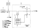
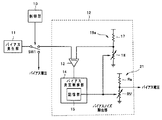
図1は本発明の第1の実施の形態に係るバイアス生成回路を示している。図1において、バイアス発生部11は、素子又は回路等に供給するためのバイアス電圧を発生する。バイアス発生部11は、温度変化、電源電圧の変動及び素子の製造ばらつきに応じて、素子又は回路等を安定して駆動するために必要なバイアス電圧を発生する。例えば、バイアス発生部11からのバイアス電圧を図示しないトランジスタのゲートバイアス電圧として利用する。この場合には、バイアス発生部11は、電源電圧の変動、温度変化及び製造ばらつき等に拘わらず、例えば、バイアス電圧を供給するトランジスタのトランスコンダクンス(gm)が一定になるようなバイアス電圧を発生することができるようになっている。
(First embodiment)
FIG. 1 shows a bias generation circuit according to a first embodiment of the present invention. In FIG. 1, a
バイアス発生部11が発生したバイアス電圧(以下、元バイアス電圧という)は、スイッチSW1を介して出力されるようになっている。スイッチSW1は、制御部10に制御されて、バイアス発生部11からの元バイアス電圧の出力先を切換える。即ち、制御部10は、スイッチSW1を制御して、元バイアス電圧を直接対象となる素子又は回路等にバイアス電圧として供給するか又はバイアスノイズ除去部12によってノイズを除去した後対象となる素子又は回路等に供給するようになっている。
A bias voltage generated by the bias generator 11 (hereinafter referred to as an original bias voltage) is output via the switch SW1. The switch SW <b> 1 is controlled by the
バイアスノイズ除去部12は、コンパレータ13、バイアス決定制御部14及びバイアス生成部16によって構成されている。バイアス生成部16は、抵抗17及び可変抵抗部18による抵抗分割回路によって構成されている。抵抗17の一端は電源端子に接続され他端は可変抵抗部18を介して基準電位点に接続される。電源端子に現れる電源電圧は、抵抗17と可変抵抗部18とによる抵抗分割によって分圧され、抵抗17と可変抵抗部18との接続点には、抵抗17の抵抗値と可変抵抗部18の抵抗値との抵抗比に基づく電圧が現れる。
The bias
バイアス生成部16は、抵抗17と可変抵抗部18との接続点に現れる電圧を、バイアス電圧として対象となる素子又は回路等に出力するようになっている。従って、可変抵抗部18の抵抗値を適宜設定することで、所望のバイアス電圧を得ることができる。このバイアス電圧は、抵抗17及び可変抵抗部18の抵抗に基づいて生成されるので、フリッカノイズレベルは十分に低い。また、バイアス電圧は、抵抗17及び可変抵抗部18の抵抗比に応じた値になるので、抵抗17及び可変抵抗部18の抵抗値を比較的小さな値に設定してもよい。抵抗に生じるノイズは、抵抗値に応じて増減するので、抵抗値を小さな値に設定することで、バイアス電圧のノイズを更に一層低減させることが可能である。
The
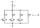
図2はバイアス生成部16の具体的な構成の一例を示す回路図である。本実施の形態においては、可変抵抗部18は、抵抗とスイッチを構成するMOSトランジスタとの直列回路を複数並列接続することによって構成される。即ち、図2の例では、抵抗R1とトランジスタQ1との直列回路、抵抗R2とトランジスタQ2との直列回路、抵抗R3とトランジスタQ3との直列回路及び抵抗R4が相互に並列接続されて、可変抵抗部18が構成されている。
FIG. 2 is a circuit diagram showing an example of a specific configuration of the
また、図2の例では、抵抗が並列に接続されている例を示したが、例えば、直列に接続された抵抗をスイッチで切換えてもよく、抵抗を可変であれば、どのようなものでも採用可能である。 In the example of FIG. 2, an example is shown in which the resistors are connected in parallel. For example, the resistors connected in series may be switched by a switch, and any resistor can be used as long as the resistors are variable. It can be adopted.
トランジスタQ1〜Q3には、後述するバイアス決定制御部14からバイアス決定データが供給される。トランジスタQ1〜Q3は、バイアス決定データのハイレベル(以下、Hレベルという)によってオンとなり、ローレベル(以下、Lレベル)によってオフとなる。バイアス決定データに基づいてトランジスタQ1〜Q3がオン,オフすることで、可変抵抗部18の合成抵抗値が決定する。抵抗R1〜R3の各抵抗値R1〜R3を相互に異なる値に設定してトランジスタQ1〜Q3を適宜オン,オフすることで、図2の可変抵抗部18は合成抵抗値としては8種類の値をとることができる。これにより、図2の可変抵抗部18を用いたバイアス生成部16は、8種類のバイアス電圧を発生することができる。
Bias determination data is supplied to the transistors Q1 to Q3 from a
コンパレータ13にはバイアス発生部11が発生した元バイアス電圧と、抵抗17と可変抵抗部18との接続点に現れるバイアス電圧とが与えられ、コンパレータ13は、2入力を比較して比較結果をバイアス決定制御部14に出力するようになっている。
The
バイアス決定制御部14は、コンパレータ13の比較結果が与えられて、バイアス生成部16において発生させるバイアス電圧を元バイアス電圧に近づけるように、可変抵抗部18を制御するバイアス決定データを求めて、記憶部15に記憶させるようになっている。記憶部15に記憶されたバイアス決定データが可変抵抗部18に供給されて、可変抵抗部18の合成抵抗値が設定されるようになっている。
The bias
即ち、本実施の形態におけるバイアス決定制御部14は、バイアス発生部11からの所定の時点における元バイアス電圧を複製した電圧をバイアス生成部16に発生させるように、バイアス決定データを求める。
That is, the bias
なお、バイアス決定制御部14は、所定のタイミングでバイアス決定データを求め、以後求めたバイアス決定データを記憶部15に保持させるようになっている。また、バイアス決定制御部14は、所定の周期毎にバイアス決定データを求めるようにしてもよく、バイアス電圧の供給対象となるシステムに応じたタイミングで、バイアス決定データを求めればよい。
The bias
なお、バイアス決定制御部14は、フリッカノイズの周波数に比べて十分に高速動作が可能であり、フリッカノイズの影響を受けることなくバイアス決定データを求めることが可能である。
The bias
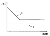
図3は横軸に周波数をとり縦軸にレベルをとって、バイアス電圧のノイズ特性を示すグラフである。図3の特性Aは、バイアス発生部11からの元バイアス電圧のノイズ特性を示し、図3の特性Bは、バイアス生成部16が発生するバイアス電圧のノイズ特性を示している。
FIG. 3 is a graph showing the noise characteristics of the bias voltage, with the horizontal axis representing frequency and the vertical axis representing level. A characteristic A in FIG. 3 indicates a noise characteristic of the original bias voltage from the
バイアス発生部11のように複雑な動作が要求される場合には、バイアス発生部11を構成する各トランジスタのサイズは、各トランジスタに要求される特性に応じて決定する必要があり、結果的に、各トランジスタのフリッカノイズは大きい。このため、図3の特性Aに示すように、元バイアス電圧には特に低い周波数において大きいレベルのノイズが重畳されている。
When a complicated operation is required like the
これに対し、可変抵抗部18を構成するトランジスタQ1〜Q3のように、トランジスタが単なるスイッチとして用いられる場合には、トランジスタの設計の自由度が高く、トランジスタのサイズを大きくすることで、フリッカノイズを低減可能である。これにより、可変抵抗部18によるノイズの影響を十分に小さくすることができ、図3の特性Bに示すように、バイアス電圧は周波数に拘わらず、そのノイズレベルは十分に低い。なお、可変抵抗部18をアナログ回路によって構成することも可能であるが、この場合にはノイズの影響を十分に低減させることはできない。
On the other hand, when the transistors are used as mere switches such as the transistors Q1 to Q3 constituting the
バイアス決定制御部14は、例えば、フラッシュ型のA/D変換器と同様の手法によってバイアス決定データを求めてもよく、また、逐次比較型(SAR:Successive Approximation Register)のA/D変換器と同様の手法によってバイアス決定データを求めてもよい。
For example, the bias
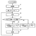
次に、このように構成された実施の形態の動作について図4のフローチャートを参照して説明する。図4は、バイアス決定制御部14が、逐次比較型のA/D変換器と同様の手法によってバイアス決定データを求める場合の動作フローを示している。
Next, the operation of the embodiment configured as described above will be described with reference to the flowchart of FIG. FIG. 4 shows an operation flow when the bias
図4の例は、可変抵抗部18のトランジスタQ1〜Q3のゲートに与えるレベルを論理値によって記憶部15に記憶させるものである。即ち、記憶部15に記憶させるバイアス決定データの論理値“1”でHレベルのゲート電圧が各トランジスタQ1〜Q3に与えられ、論理値“0”でLレベルのゲート電圧がトランジスタQ1〜Q3に与えられるようになっている。バイアス決定データは、トランジスタQ1〜Q3に夫々対応したビットによって構成される。バイアス決定制御部14は、可変抵抗部18の各抵抗R1〜R3のうち、バイアス電圧を最も大きく減少させる抵抗に対してバイアス決定データの最上位ビットを割当て、バイアス電圧の減少への寄与が小さい抵抗ほど下位のビットを割り当てる。なお、図2の例ではバイアス決定データは3ビットである。
In the example of FIG. 4, the level given to the gates of the transistors Q <b> 1 to Q <b> 3 of the
バイアス発生部11は、対象となる素子又は回路等に供給するバイアス電圧を発生する。バイアス発生部11は、温度変化、電源電圧の変動及び製造ばらつき等に対して最適な値となるように、バイアス電圧を変化させている。しかし、バイアス発生部11からのバイアス電圧は、フリッカノイズによって、特に低周波域においてレベル変動が比較的大きい。
The
制御部10は、所定のタイミングでスイッチSW1を制御して、バイアス発生部11からのバイアス電圧を元バイアス電圧としてバイアスノイズ除去部12に与える。バイアスノイズ除去部12は、バイアス決定制御部14によって、元バイアス電圧からノイズを除去したバイアス電圧を発生して、対象となる素子又は回路等に供給する。
The
図4はバイアスノイズ除去部12の動作を示している。先ず、バイアス決定制御部14は、ステップS1においてバイアス決定データの各ビットを初期化して“0”とする。即ち、この場合には、可変抵抗部18は最大の抵抗値となり、バイアス生成部16は、電源電圧と抵抗17,R4に基づく最大のバイアス電圧が得られる。
FIG. 4 shows the operation of the bias
次に、バイアス決定制御部14は、バイアス決定データの最上位ビットを“1”にする(ステップS2)。記憶部15には最上位ビットが“1”で他のビットが“0”のバイアス決定データが記憶される。
Next, the bias
記憶部15に記憶されたバイアス決定データは可変抵抗部18のトランジスタQ1〜Q3に供給される。バイアス電圧を最も大きく減少させる抵抗に接続されたトランジスタには、Hレベルが供給され、可変抵抗部18の合成抵抗は、当該抵抗と抵抗R4とに基づくものとなる。これにより、バイアス生成部16からのバイアス電圧は低下する。
The bias determination data stored in the
コンパレータ13はこの状態で、元バイアス電圧とバイアス生成部16からのバイアス電圧とを比較する(ステップS3)。バイアス決定制御部14は、コンパレータ13の比較結果に基づいて、元バイアス電圧がバイアス電圧よりも小さいか否かを判定する(ステップS4)。
In this state, the
元バイアス電圧の方が小さい場合には、バイアス決定制御部14は、最上位ビットを“1”のままとし、次の下位ビットを“1”にする(ステップS5)。このバイアス決定データが記憶部15に記憶され(ステップS7)、記憶されたバイアス決定データに基づいて可変抵抗部18が制御されると、バイアス電圧は一層低下する。
When the original bias voltage is smaller, the bias
逆に、ステップS4において元バイアス電圧の方が大きいと判定された場合には、バイアス決定制御部14は、最上位ビットを“0”に戻して、次の下位ビットを“1”にする(ステップS6)。このバイアス決定データが記憶部15に記憶されて可変抵抗部18が制御されると、バイアス電圧は最大のバイアス電圧から“1”にした下位ビットの分だけ小さくなる。
Conversely, if it is determined in step S4 that the original bias voltage is higher, the bias
以後同様にして、ステップS2〜S6を実行して、コンパレータ13によって、バイアス電圧と元バイアス電圧とを逐次比較しながら、バイアス電圧を変化させる。
Thereafter, similarly, Steps S2 to S6 are executed, and the
そして、バイアス決定制御部14は、バイアス決定データの最上位ビットから順次下位ビットを決定する。こうして、バイアス決定制御部14は、バイアス決定データの3つのビットを求める。こうして求められたバイアス決定データによってトランジスタQ1〜Q3をオン,オフ制御することにより、バイアス電圧を元バイアス電圧に近づけることができる。
Then, the bias
バイアス生成部16からのバイアス電圧は、バイアス発生部11からの元バイアス電圧に近い値であり、且つ、バイアス生成部16が抵抗分割によってバイアス電圧を得ていることから、ノイズは低く周波数特性も平坦である。
The bias voltage from the
元バイアス電圧は低周波域において大きなレベルのノイズが混入している。時間的にみると、元バイアス電圧は低い周波数で比較的大きくレベル変動していることになる。仮に、このような元バイアス電圧を電圧制御発振器のバイアス電流に利用した場合には、バイアス電流に発生する低周波ノイズによって、電圧制御発振器の発振出力の位相ノイズが大きくなり、周波数が比較的大きく変動してしまう。 The original bias voltage is mixed with a large level of noise in the low frequency range. In terms of time, the level of the original bias voltage is relatively large at a low frequency. If such an original bias voltage is used for the bias current of the voltage controlled oscillator, the low frequency noise generated in the bias current increases the phase noise of the oscillation output of the voltage controlled oscillator, and the frequency is relatively large. It will fluctuate.
これに対し、バイアス生成部16によって生成されたバイアス電圧は、低周波域のノイズが十分に小さい。従って、このような低ノイズのバイアス電圧を電圧制御発振器に利用することで、電圧発振器の発振周波数を安定したものとすることが可能である。
On the other hand, the bias voltage generated by the
しかし、バイアス生成部16単体では、温度変化、電源電圧の変動及び製造ばらつき等に応じてバイアス電圧を変化させることはできない。そこで、本実施の形態においては、バイアス決定制御部14は、適宜のタイミングで、元バイアス電圧からノイズを除去したバイアス電圧を得る。バイアス発生部11は、温度変化、電源電圧の変動及び製造ばらつき等に応じた元バイアス電圧を発生しており、バイアス生成部16は、温度変化、電源電圧の変動等に応じて変化したバイアス電圧を生成することが可能である。
However, the
例えば、バイアス決定制御部14は、バイアス電圧供給対象の回路が送信回路である場合において、送信時の直前に元バイアス電圧からノイズを除去したバイアス電圧を生成して、例えば電圧制御発振器に供給するようにしてもよい。
For example, when the bias voltage supply target circuit is a transmission circuit, the bias
また、例えば、制御部10において、送信時の直前から送信が終了するまでの期間のみ、元バイアス電圧をバイアスノイズ除去部12に与えるようにしてもよい。一般的には、電圧制御発振器が送信のために発振する時間は比較的短く、この時間に温度上昇等の変化は極めて小さいものと考えられる。従って、制御部10が例えば所定の期間にのみ元バイアス電圧をバイアスノイズ除去部12に与えるようにすることで、バイアス生成部16において温度変化に応じたバイアス電圧を生成することが可能である。
Further, for example, the
例えば、ブルートゥース送信機においては、周波数ホッピングのために発振周波数が変更される。周波数変更時には、電圧制御発振器の発振周波数がロックするまでの間、送信は行われないので、例えばこの期間に、バイアス決定制御部14においてバイアス決定データを求めて、バイアス電圧を生成するようにしてもよい。
For example, in a Bluetooth transmitter, the oscillation frequency is changed for frequency hopping. When the frequency is changed, transmission is not performed until the oscillation frequency of the voltage controlled oscillator is locked. For example, during this period, the bias
また、バイアス決定制御部14は、バイアス決定データを装置の起動時のみ一度だけ求め、以後、求めたバイアス決定データに基づくバイアス電圧を生成するようにしてもよい。この場合でも、製造ばらつきを補償することができる。
Further, the bias
このように本実施の形態においては、温度変化、電源電圧の変動及び製造ばらつき等に対応したバイアス電圧を発生するバイアス発生部を利用し、所定タイミングにおけるバイアス電圧の値を求めて、抵抗分割によって復元することにより、フリッカノイズを低減した安定したバイアス電圧であって、且つ、温度変化、電源電圧の変動及び製造ばらつき等に対応したバイアス電圧を得ている。コンパレータやバイアス決定制御部等の追加回路の面積は十分に小さく、また、バイアス電圧のノイズ除去のためにカットオフ周波数が低い大面積のローパスフィルタ等を構成する必要が無いことから、小さい面積で低雑のバイアス電圧を発生するバイアス生成回路を構成する半導体集積回路装置が得られる。 As described above, in the present embodiment, a bias generation unit that generates a bias voltage corresponding to a temperature change, a power supply voltage variation, a manufacturing variation, and the like is used to obtain a bias voltage value at a predetermined timing and perform resistance division. By restoring, a stable bias voltage with reduced flicker noise and a bias voltage corresponding to temperature change, power supply voltage fluctuation, manufacturing variation, and the like are obtained. The area of the additional circuits such as the comparator and the bias determination control unit is sufficiently small, and it is not necessary to configure a large-area low-pass filter with a low cut-off frequency to remove noise from the bias voltage. A semiconductor integrated circuit device constituting a bias generation circuit that generates a low bias voltage can be obtained.
なお、本実施の形態におけるバイアス生成回路は、バイアス電圧を生成するものである。バイアス電流は、例えば1個のトランジスタのゲートに印加するバイアス電圧を制御することで得られる。従って、本実施の形態においては、バイアス電流の生成については説明を省略するが、図1のバイアス電圧を用いることで、容易にノイズを除去したバイアス電流を生成することができることは明らかである。 Note that the bias generation circuit in the present embodiment generates a bias voltage. The bias current can be obtained, for example, by controlling the bias voltage applied to the gate of one transistor. Therefore, in this embodiment, the description of the generation of the bias current is omitted, but it is obvious that the bias current from which noise is removed can be easily generated by using the bias voltage of FIG.
また、上記実施の形態においては、バイアス生成回路は、トランジスタ素子のトランスコンダクタンス(gm)を一定にするためのバイアス電圧を発生する例を示したが、本発明はこれに限ったものではなく、例えばトランジスタ素子のドレイン電流を一定にするためのバイアス電圧を発生するようにしてもよい。 In the above embodiment, the bias generation circuit generates the bias voltage for making the transconductance (gm) of the transistor element constant. However, the present invention is not limited to this. For example, a bias voltage for making the drain current of the transistor element constant may be generated.
(第2の実施の形態)
図5は本発明の第2の実施の形態を示す回路図である。図5において図1と同一の構成要素には同一符号を付して説明を省略する。
(Second Embodiment)
FIG. 5 is a circuit diagram showing a second embodiment of the present invention. In FIG. 5, the same components as those of FIG.
本実施の形態は、バイアス生成部16に代えて抵抗分割部16aを採用すると共に、出力部21を付加した点が第1の実施の形態と異なる。抵抗分割部16aはバイアス生成部16と同一構成である。出力部21は、電源端子と基準電位点との間に直列接続された抵抗Ra及び可変抵抗部RVによって構成され、可変抵抗部RVは、その抵抗値がバイアス決定制御部14からのバイアス決定データに基づいて決定されるようになっている。例えば、出力部21は、バイアス生成部16と同一に構成されて、バイアス決定制御部14からのバイアス決定データに基づいてバイアス電圧を生成する。
The present embodiment is different from the first embodiment in that a
図1のバイアス生成部16は、対象となる素子又は回路等に供給するバイアス電圧を生成する機能を有すると共に、バイアス決定データを求めるために、元バイアス電圧と比較される電圧を生成する比較電圧生成機能を有する。これに対し、本実施の形態においては、出力部21によってバイアス電圧は生成されるので、抵抗分割部16aとしては、比較電圧生成機能のみを有していればよい。
The
従って、抵抗分割部16aと出力部21とを同一構成とする必要はない。例えば、出力部21の抵抗Raと可変抵抗部RVとの抵抗比を、抵抗R17と可変抵抗R18との抵抗比に一致させればよく、出力部21の抵抗Ra及び可変抵抗部RVとの各抵抗値を、抵抗R17及び可変抵抗R18の抵抗値に一致させる必要はない。
Therefore, it is not necessary that the
例えば、出力部21の抵抗Ra及び可変抵抗部RVとの各抵抗値を、抵抗R17及び可変抵抗R18の抵抗値よりも小さくすることが考えられる。この場合には、バイアス決定データを求める期間においては、抵抗分割部16aの比較的大きな抵抗値によって消費電力を抑制すると共に、出力部21の比較的小さい抵抗値によって、ノイズの影響を小さくすることができる。
For example, it is conceivable that the resistance values of the resistor Ra and the variable resistor portion RV of the
また、抵抗分割部16aは、比較電圧生成機能のみを有していればよいので、必ずしも抵抗とスイッチとの直列回路を複数並列接続して構成する必要はなく、例えばアナログ回路によって構成することも可能である。
Further, since the
他の構成及び作用効果は第1の実施の形態と同様である。 Other configurations and operational effects are the same as those of the first embodiment.
このように本実施の形態においては、第1の実施の形態よりも設計の自由度が向上すると共に、消費電力を抑制しながら低ノイズのバイアス電圧を生成することが可能である。 As described above, in this embodiment, the degree of freedom in design is improved as compared with the first embodiment, and a low-noise bias voltage can be generated while suppressing power consumption.
なお、上述したように、電圧制御発振器のバイアス電流に低周波ノイズが混入すると、電圧制御発振器の発振出力の位相ノイズが大きくなり、周波数変動が発生する。このため、上記各実施の形態において示した電圧制御発振器をバイアス電流の生成に利用することで、安定した発振周波数を得ることができ、極めて有用である。 As described above, when low-frequency noise is mixed in the bias current of the voltage controlled oscillator, the phase noise of the oscillation output of the voltage controlled oscillator increases and frequency fluctuation occurs. Therefore, a stable oscillation frequency can be obtained by using the voltage controlled oscillator shown in each of the above embodiments for generating a bias current, which is extremely useful.
(第3の実施の形態)
図6は本発明の第3の実施の形態を示す回路図である。図6はLSI化に適した電圧制御発振器を示している。図6において図2と同一の構成要素には同一符号を付して説明を省略する。
(Third embodiment)
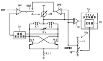
FIG. 6 is a circuit diagram showing a third embodiment of the present invention. FIG. 6 shows a voltage controlled oscillator suitable for LSI implementation. In FIG. 6, the same components as those of FIG.
電圧制御発振器においては、単にバイアス電流を所望の値に制御しただけでは、発振周波数が変化する毎に発振振幅が変化してしまう。この問題に対し、特許文献2においては、発振周波数に拘わらず、発振振幅を一定にする技術が開示されている。
In a voltage controlled oscillator, simply controlling the bias current to a desired value changes the oscillation amplitude every time the oscillation frequency changes. To deal with this problem,
しかし、特許文献2の発明においても、発振トランジスタに生じるフリッカノイズ及びバイアス電流制御のための基準電圧(REF)のノイズによって、バイアス電流に低周波ノイズが混入してしまう。そうすると、発振出力の位相ノイズが増大する。
However, even in the invention of
本実施の形態においては、発振周波数に拘わらず発振振幅が一定の電圧制御発振器において、バイアス電流の低周波ノイズを抑制して、発振出力の位相ノイズを抑制することを可能にしたものである。 In this embodiment, in a voltage controlled oscillator having a constant oscillation amplitude regardless of the oscillation frequency, it is possible to suppress low frequency noise of the bias current and suppress phase noise of the oscillation output.
図6において、電圧制御発振器は、コイルL1,L2、バラクタ等の可変容量素子Cv発振トランジスタM1,M2を有している。電源端子とコイルL1,L2の接続点との間には電流源32が接続されており、コイルL1,L2の接続点には、電流源32からドレイン電流(バイアス電流)が供給されるようになっている。
In FIG. 6, the voltage controlled oscillator has coils L1 and L2 and variable capacitance elements Cv oscillation transistors M1 and M2 such as varactors. A
コイルL1及びL2の直列回路の一端は発振トランジスタM1のドレインに接続され、他端は、発振トランジスタM2のドレインに接続される。差動対を成すトランジスタM1,M2のソースは共通接続されて、その接続点は抵抗R11を介して基準電位点に接続される。トランジスタM1のドレインはトランジスタM2のゲートに接続され、トランジスタM2のドレインはトランジスタM1のゲートに接続される。 One end of the series circuit of the coils L1 and L2 is connected to the drain of the oscillation transistor M1, and the other end is connected to the drain of the oscillation transistor M2. The sources of the transistors M1 and M2 forming the differential pair are commonly connected, and the connection point is connected to the reference potential point via the resistor R11. The drain of the transistor M1 is connected to the gate of the transistor M2, and the drain of the transistor M2 is connected to the gate of the transistor M1.
図6の電圧制御発振器は、コイルL1,L2及び可変容量素子CvによるLC共振回路によって発振周波数が決定される。発振トランジスタM1,M2のドレインに、発振出力が現れる。電圧制御発振器は、可変容量素子Cvの容量値を基準周波数に基づいて変化させることで、発振周波数が基準周波数に対応した周波数に一致するようになっている。 In the voltage controlled oscillator of FIG. 6, the oscillation frequency is determined by an LC resonance circuit including the coils L1 and L2 and the variable capacitance element Cv. An oscillation output appears at the drains of the oscillation transistors M1 and M2. The voltage controlled oscillator changes the capacitance value of the variable capacitance element Cv based on the reference frequency, so that the oscillation frequency matches the frequency corresponding to the reference frequency.
発振トランジスタM1,M2のドレインは振幅検出回路31に接続されている。振幅検出回路31は、発振振幅を検出して、発振振幅に応じた振幅検出電圧をオペアンプOP1の負極性入力端に出力する。オペアンプOP1の正極性入力端には、電流源32の制御電圧の基準となる基準電圧(REF)が供給される。オペアンプOP1は振幅検出電圧が基準電圧に一致するように制御電圧を発生して、スイッチSW1を介して電流源32に与えてフィードバック制御する。これにより、電流源32は、発振周波数に拘わらず、発振振幅を一定にするように、バイアス電流を流す。
The drains of the oscillation transistors M1 and M2 are connected to the
しかしながら、上述したように、発振トランジスタM1,M2のフリッカノイズ及び基準電圧(REF)のノイズによって、バイアス電流に低周波ノイズが混入してしまう。本実施の形態においては、このようなバイアス電流の低周波ノイズを除去するために、コンパレータ13、バイアス決定制御部14、抵抗分割部16a、オペアンプOP2及びスイッチSW2を設けている。
However, as described above, the low-frequency noise is mixed into the bias current due to the flicker noise of the oscillation transistors M1 and M2 and the noise of the reference voltage (REF). In the present embodiment, in order to remove such low-frequency noise of the bias current, a
コンパレータ13には、コイルL1,L2の接続点に現れる直流電圧及び抵抗分割部16aによって発生される比較電圧が供給され、コンパレータ13は2入力の比較結果をバイアス決定制御部14に出力する。バイアス決定制御部14は、比較結果に基づいて可変抵抗部18の抵抗値を制御するバイアス決定データを求めて、記憶部15に保持させる。記憶部15からのバイアス決定データに基づいて、抵抗分割部16aは、所定のタイミングにおけるコイルL1,L2の接続点に現れる直流電圧に近い電圧値の比較電圧を出力する。
The
即ち、コイルL1,L2の接続点に現れる直流電圧は、バイアス電流の低周波ノイズの影響によって低周波ノイズが混入している。これに対し、可変抵抗部18からの比較電圧は、コイルL1,L2の接続点に現れる直流電圧の低周波ノイズを除去した電圧となる。
That is, the DC voltage appearing at the connection point between the coils L1 and L2 is mixed with low frequency noise due to the influence of the low frequency noise of the bias current. On the other hand, the comparison voltage from the
オペアンプOP2の正極性入力端には比較電圧が供給され、負極性入力端にはコイルL1,L2の接続点に現れる直流電圧が供給される。オペアンプOP2は、コイルL1,L2の接続点に現れる直流電圧が比較電圧に一致するように、電流源32を制御するための制御電圧をスイッチSW2を介して電流源32に供給する。
A comparison voltage is supplied to the positive input terminal of the operational amplifier OP2, and a DC voltage appearing at the connection point of the coils L1 and L2 is supplied to the negative input terminal. The operational amplifier OP2 supplies a control voltage for controlling the
次に、このように構成された実施の形態の動作について説明する。 Next, the operation of the embodiment configured as described above will be described.
発振周波数を変更する場合には、発振周波数がロックするまでの間、発振出力は、通信等に利用されない、あるいは、利用される場合にも、雑音が小さいことはさほど要求されない。本実施の形態においては、例えば発振周波数がロックするまでの期間において、バイアス決定データを求めて比較電圧を決定するようになっている。即ち、この期間には、スイッチSW2は、オペアンプOP1の出力を電流源32に供給する。トランジスタM1,M2のドレインに現れる発振出力の振幅は振幅検出回路31によって検出される。オペアンプOP1は、振幅検出電圧が基準電圧(REF)に一致するように、電流源32を制御する制御電圧を発生する。
When the oscillation frequency is changed, the oscillation output is not used for communication or the like until the oscillation frequency is locked, or even when used, it is not required that the noise is small. In the present embodiment, for example, during the period until the oscillation frequency locks, the bias determination data is obtained to determine the comparison voltage. That is, during this period, the switch SW2 supplies the output of the operational amplifier OP1 to the
このように、電流源32は、オペアンプOP1に制御されて、トランジスタM1,M2のドレインに現れる発振出力の振幅が一定となるようなドレイン電流を出力する。このドレイン電流には、低周波ノイズが含まれる。
In this way, the
ドレイン電流に応じてコイルL1,L2の接続点に現れる直流電圧は、コンパレータ13に供給される。コンパレータ13は抵抗分割部16aからの比較電圧とコイルL1,L2の接続点に現れる直流電圧とを比較し、比較結果をバイアス決定制御部14に出力する。バイアス決定制御部14は、比較電圧がコイルL1,L2の接続点に現れる直流電圧に近づけるように、抵抗分割部16aの可変抵抗部18の抵抗値を制御するためのバイアス決定データを求める。バイアス決定データは記憶部15に記憶され、可変抵抗部18は記憶部15に記憶されたバイアス決定データに基づいて抵抗値が決定される。
The DC voltage that appears at the connection point of the coils L1 and L2 according to the drain current is supplied to the
こうして、抵抗分割部16aからの比較電圧は、所定のタイミングにおけるコイルL1,L2の接続点に現れる直流電圧値に近い値となる。即ち、比較電圧は、コイルL1,L2の接続点に現れる直流電圧の低周波ノイズを除去した電圧となる。
Thus, the comparison voltage from the
次に、発振出力を通信等に利用するために、雑音が小さい動作モードに移行する。スイッチSW2はオペアンプOP2の出力を電流源32に供給する。またこの期間には、抵抗分割部16aは記憶部15に記憶されているバイアス決定データに基づいて比較電圧を発生する。
Next, in order to use the oscillation output for communication or the like, the operation mode is shifted to a low noise operation mode. The switch SW2 supplies the output of the operational amplifier OP2 to the
オペアンプOP2は、コイルL1,L2の接続点に現れる直流電圧が比較電圧に一致するように、電流源32を制御する制御電圧を発生する。比較電圧の低周波ノイズは十分に抑圧されており、電流源32からのドレイン電流の低周波ノイズは十分に低いレベルとなる。これにより、トランジスタM1,M2のドレインからは、安定した発振周波数の発振出力が得られる。また、オペアンプOP2からの制御電圧は、発振周波数に拘わらず発振出力の振幅を一定にすることを可能にするものであり、図6の電圧制御発振器は、周波数に拘わらず一定振幅で且つ位相ノイズが十分に低減された発振出力を出力することができる。
The operational amplifier OP2 generates a control voltage for controlling the
なお、バイアス決定制御部14は、少なくとも発振周波数の変更毎に、バイアス決定データを求めるようにした方がよい。
It is preferable that the bias
このように本実施の形態においては、周波数に拘わらず一定振幅で且つ位相ノイズが十分に低減された発振出力を得る電圧制御発振器を提供することができる。 As described above, in this embodiment, it is possible to provide a voltage controlled oscillator that obtains an oscillation output with a constant amplitude and a sufficiently reduced phase noise regardless of the frequency.
10…制御部、11…バイアス発生部、12…バイアスノイズ除去部、13…コンパレータ、14…バイアス決定制御部、15…記憶部、16…バイアス生成部、17…抵抗、18…可変抵抗部。
DESCRIPTION OF
Claims (5)
前記元バイアス電圧と比較電圧とを比較し、比較結果を出力する比較部と、
抵抗とスイッチで構成された可変抵抗部を含む抵抗回路によって構成されて前記比較電圧を発生する抵抗分割部と、
前記比較部の比較結果に基づいて、前記比較電圧を前記元バイアス電圧に近づけるように前記可変抵抗部の抵抗値を制御するためのバイアス決定データを求めるバイアス決定制御部と、
前記バイアス決定データを保持して前記可変抵抗部の抵抗値を制御することにより前記比較電圧をバイアス電圧として出力させる記憶部と
を具備したことを特徴とするバイアス生成回路。 A bias generator for generating an original bias voltage;
A comparison unit that compares the original bias voltage with a comparison voltage and outputs a comparison result;
A resistance dividing unit configured to generate the comparison voltage by a resistance circuit including a variable resistance unit configured by a resistor and a switch;
A bias determination control unit for obtaining bias determination data for controlling a resistance value of the variable resistance unit so as to bring the comparison voltage closer to the original bias voltage based on a comparison result of the comparison unit;
And a storage unit that holds the bias determination data and controls the resistance value of the variable resistance unit to output the comparison voltage as a bias voltage.
を具備したことを特徴とする請求項1に記載のバイアス生成回路。 2. The bias generation circuit according to claim 1, further comprising: an output unit configured by a resistance divider circuit configured to have the same resistance ratio as the resistance ratio of the resistor divider for generating the comparison voltage. .
前記ドレイン電流に基づく直流電圧と比較電圧とを比較し、比較結果を出力する比較部と、
可変抵抗部を含む抵抗回路によって構成されて前記比較電圧を発生する抵抗分割部と、
前記比較部の比較結果に基づいて、前記比較電圧を前記ドレイン電流に基づく直流電圧に近づけるように前記可変抵抗部の抵抗値を制御するためのバイアス決定データを求めるバイアス決定制御部と、
前記バイアス決定データを保持して前記可変抵抗部の抵抗値を制御することにより前記抵抗分割部から前記比較電圧を出力させる記憶部と、
前記ドレイン電流に基づく直流電圧を前記比較電圧に一致させるように前記電流源を制御する演算増幅器と
を具備したことを特徴とする電圧制御発振器。 A voltage controlled oscillator comprising: a resonance circuit that determines an oscillation frequency; an oscillation MOS transistor that is connected to the resonance circuit and outputs an oscillation output of the oscillation frequency; and a current source that supplies a drain current of the oscillation MOS transistor When,
A comparison unit that compares the direct current voltage based on the drain current with a comparison voltage and outputs a comparison result;
A resistance divider configured to generate the comparison voltage by a resistor circuit including a variable resistor; and
A bias determination control unit for obtaining bias determination data for controlling a resistance value of the variable resistor unit so as to bring the comparison voltage close to a DC voltage based on the drain current based on a comparison result of the comparison unit;
A storage unit for holding the bias determination data and controlling the resistance value of the variable resistance unit to output the comparison voltage from the resistance dividing unit;
An operational amplifier that controls the current source so that a DC voltage based on the drain current matches the comparison voltage.
前記発振MOSトランジスタのドレインに現れる発振出力の振幅を検出する振幅検出部と、
前記振幅検出部の検出結果が所定の基準電圧に一致するように前記電流源を制御するための第1の制御信号を発生する第1の演算増幅器と、
前記ドレイン電流に基づく直流電圧と比較電圧とを比較し、比較結果を出力する比較部と、
可変抵抗部を含む抵抗回路によって構成されて前記比較電圧を発生する抵抗分割部と、
前記比較部の比較結果に基づいて、前記比較電圧を前記ドレイン電流に基づく直流電圧に近づけるように前記可変抵抗部の抵抗値を制御するためのバイアス決定データを求めるバイアス決定制御部と、
前記バイアス決定データを保持して前記可変抵抗部の抵抗値を制御することにより前記抵抗分割部から前記比較電圧を出力させる記憶部と、
前記ドレイン電流に基づく直流電圧が前記比較電圧に一致するように前記電流源を制御するための第2の制御信号を発生する第2の演算増幅器と、
前記第1又は第2の制御信号を選択的に前記電流源に与える切換部と
を具備したことを特徴とする電圧制御発振器。 A voltage controlled oscillator comprising: a resonance circuit that determines an oscillation frequency; an oscillation MOS transistor that is connected to the resonance circuit and outputs an oscillation output of the oscillation frequency; and a current source that supplies a drain current of the oscillation MOS transistor When,
An amplitude detector for detecting the amplitude of the oscillation output appearing at the drain of the oscillation MOS transistor;
A first operational amplifier that generates a first control signal for controlling the current source so that a detection result of the amplitude detector matches a predetermined reference voltage;
A comparison unit that compares the direct current voltage based on the drain current with a comparison voltage and outputs a comparison result;
A resistance divider configured to generate the comparison voltage by a resistor circuit including a variable resistor; and
A bias determination control unit for obtaining bias determination data for controlling a resistance value of the variable resistor unit so as to bring the comparison voltage close to a DC voltage based on the drain current based on a comparison result of the comparison unit;
A storage unit for holding the bias determination data and controlling the resistance value of the variable resistance unit to output the comparison voltage from the resistance dividing unit;
A second operational amplifier for generating a second control signal for controlling the current source so that a DC voltage based on the drain current matches the comparison voltage;
A voltage-controlled oscillator comprising: a switching unit that selectively applies the first or second control signal to the current source.
Priority Applications (2)
| Application Number | Priority Date | Filing Date | Title |
|---|---|---|---|
| JP2009065289A JP4929306B2 (en) | 2009-03-17 | 2009-03-17 | Bias generation circuit and voltage controlled oscillator |
| US12/555,985 US7999628B2 (en) | 2009-03-17 | 2009-09-09 | Bias generation circuit and voltage controlled oscillator |
Applications Claiming Priority (1)
| Application Number | Priority Date | Filing Date | Title |
|---|---|---|---|
| JP2009065289A JP4929306B2 (en) | 2009-03-17 | 2009-03-17 | Bias generation circuit and voltage controlled oscillator |
Publications (2)
| Publication Number | Publication Date |
|---|---|
| JP2010219964A JP2010219964A (en) | 2010-09-30 |
| JP4929306B2 true JP4929306B2 (en) | 2012-05-09 |
Family
ID=42737023
Family Applications (1)
| Application Number | Title | Priority Date | Filing Date |
|---|---|---|---|
| JP2009065289A Expired - Fee Related JP4929306B2 (en) | 2009-03-17 | 2009-03-17 | Bias generation circuit and voltage controlled oscillator |
Country Status (2)
| Country | Link |
|---|---|
| US (1) | US7999628B2 (en) |
| JP (1) | JP4929306B2 (en) |
Families Citing this family (12)
| Publication number | Priority date | Publication date | Assignee | Title |
|---|---|---|---|---|
| US8686798B2 (en) * | 2011-05-19 | 2014-04-01 | Freescale Semiconductor, Inc. | Method and system for testing oscillator circuit |
| JP5684080B2 (en) * | 2011-09-22 | 2015-03-11 | 株式会社東芝 | Analog / digital converter |
| JP6646227B2 (en) | 2014-08-28 | 2020-02-14 | 株式会社ソシオネクスト | Bias generation circuit, voltage generation circuit, communication equipment, and radar equipment |
| US20160095226A1 (en) * | 2014-09-30 | 2016-03-31 | Thin Film Electronics Asa | Printed Timer Label |
| EP3096450A1 (en) * | 2015-05-20 | 2016-11-23 | Aiut Sp. z o.o. | Electric circuit of a generator of oscillations |
| US9473151B1 (en) | 2015-06-05 | 2016-10-18 | Telefonaktiebolaget Lm Ericsson (Publ) | Low-noise oscillator amplitude regulator |
| US10620261B2 (en) * | 2018-05-15 | 2020-04-14 | Arm Limited Cambridge | Built-in self-test method and apparatus for single-pin crystal oscillators |
| US10564217B2 (en) | 2018-05-15 | 2020-02-18 | Arm Limited | Built-in self-test method and apparatus for single-pin crystal oscillators |
| JP7325956B2 (en) * | 2018-12-25 | 2023-08-15 | ヌヴォトンテクノロジージャパン株式会社 | RF power amplifier |
| CN111917396A (en) * | 2019-05-09 | 2020-11-10 | 复旦大学 | Broadband low-power-consumption oscillator device with self-adaptive voltage bias |
| JP7534843B2 (en) * | 2019-07-30 | 2024-08-15 | ミツミ電機株式会社 | Power supply control semiconductor device and variable output voltage power supply device |
| TWI727673B (en) * | 2020-02-25 | 2021-05-11 | 瑞昱半導體股份有限公司 | Bias current generation circuit |
Family Cites Families (18)
| Publication number | Priority date | Publication date | Assignee | Title |
|---|---|---|---|---|
| JPS62260428A (en) * | 1986-05-06 | 1987-11-12 | Mitsubishi Electric Corp | Phase-locked oscillator |
| JPH0750527A (en) * | 1993-08-09 | 1995-02-21 | Mitsubishi Electric Corp | Semiconductor integrated circuit device and bias setting method |
| US5849613A (en) * | 1997-10-23 | 1998-12-15 | Chartered Semiconductor Manufacturing Ltd. | Method and mask structure for self-aligning ion implanting to form various device structures |
| US6356161B1 (en) * | 1998-03-19 | 2002-03-12 | Microchip Technology Inc. | Calibration techniques for a precision relaxation oscillator integrated circuit with temperature compensation |
| JP2001060868A (en) * | 1999-08-19 | 2001-03-06 | Hitachi Ltd | Amplifier circuit, lc resonance circuit, voltage control oscillation circuit, pll circuit, video signal processing circuit and video tape recorder |
| GB2368735B (en) * | 2000-09-01 | 2004-07-21 | Sgs Thomson Microelectronics | Oscillator |
| JP4270339B2 (en) * | 2000-12-27 | 2009-05-27 | 富士通株式会社 | PLL circuit and automatic bias adjustment circuit used therefor |
| JP2002353749A (en) * | 2001-05-28 | 2002-12-06 | Japan Radio Co Ltd | Power amplifier circuit |
| US6582995B2 (en) * | 2001-07-11 | 2003-06-24 | Taiwan Semiconductor Manufacturing Co., Ltd. | Method for fabricating a shallow ion implanted microelectronic structure |
| US7033950B2 (en) * | 2001-12-19 | 2006-04-25 | Auburn University | Graded junction termination extensions for electronic devices |
| US7102184B2 (en) * | 2003-06-16 | 2006-09-05 | Micron Technology, Inc. | Image device and photodiode structure |
| US7303952B2 (en) * | 2004-10-04 | 2007-12-04 | International Business Machines Corporation | Method for fabricating doped polysilicon lines |
| EP1672799B1 (en) | 2004-12-17 | 2008-03-19 | Kabushiki Kaisha Toshiba | Semiconductor integrated circuit device |
| JP4922609B2 (en) * | 2004-12-17 | 2012-04-25 | 株式会社東芝 | Semiconductor integrated circuit device and wireless communication device using the same |
| JP2006238062A (en) * | 2005-02-25 | 2006-09-07 | Fuji Electric Holdings Co Ltd | Amplifier circuit |
| US7268633B2 (en) * | 2005-09-12 | 2007-09-11 | P.A. Semi, Inc. | Voltage-controlled oscillator for low-voltage, wide frequency range operation |
| US20070231710A1 (en) * | 2006-03-30 | 2007-10-04 | Texas Instruments Incorporated. | Method and system for forming a photomask pattern |
| JP2008306331A (en) | 2007-06-06 | 2008-12-18 | Toshiba Corp | Semiconductor integrated circuit device |
-
2009
- 2009-03-17 JP JP2009065289A patent/JP4929306B2/en not_active Expired - Fee Related
- 2009-09-09 US US12/555,985 patent/US7999628B2/en not_active Expired - Fee Related
Also Published As
| Publication number | Publication date |
|---|---|
| JP2010219964A (en) | 2010-09-30 |
| US7999628B2 (en) | 2011-08-16 |
| US20100237956A1 (en) | 2010-09-23 |
Similar Documents
| Publication | Publication Date | Title |
|---|---|---|
| JP4929306B2 (en) | Bias generation circuit and voltage controlled oscillator | |
| JP2008054134A (en) | Ring oscillator, semiconductor integrated circuit provided with the same, and electronic equipment | |
| US7876163B2 (en) | Voltage-controlled oscillator circuit and phase locked loop circuit using the same | |
| US7915966B2 (en) | Oscillator for controlling voltage | |
| JP2011525080A (en) | Apparatus and method for tuning a Gm-C filter | |
| JP2006510309A (en) | Temperature compensated RC oscillator | |
| JP2006339727A (en) | Voltage controlled oscillator | |
| JP2009284329A (en) | Semiconductor integrated circuit device | |
| US7301409B2 (en) | Oscillator | |
| JPH11220365A (en) | Clock multiplying circuit | |
| KR101208565B1 (en) | Voltage controlled oscillator capable of reducing phase noise and jitter with high startup gain and method thereof | |
| CN107294525B (en) | Oscillator circuit and related method thereof | |
| JPWO2004079895A1 (en) | Crystal oscillation circuit | |
| JP4636107B2 (en) | PLL circuit | |
| JP2001515290A (en) | Oscillator circuit with crystal oscillator | |
| JP2009182584A (en) | Pll circuit | |
| KR20100001696A (en) | Phase locked loop comprising improved loop filter | |
| JP2012199761A (en) | Phase-locked loop and method of controlling the same | |
| JP2009141459A (en) | Piezoelectric oscillator | |
| JP2006033238A (en) | Voltage-controlled oscillator | |
| JP2009124530A (en) | Piezoelectric oscillator | |
| KR101081384B1 (en) | Oscillator | |
| KR100834914B1 (en) | Frequency Tuning Device | |
| JP2002026658A (en) | Quartz oscillator circuit | |
| JP2015095849A (en) | Oscillator and voltage generation circuit |
Legal Events
| Date | Code | Title | Description |
|---|---|---|---|
| A621 | Written request for application examination |
Free format text: JAPANESE INTERMEDIATE CODE: A621 Effective date: 20110323 |
|
| A977 | Report on retrieval |
Free format text: JAPANESE INTERMEDIATE CODE: A971007 Effective date: 20120110 |
|
| TRDD | Decision of grant or rejection written | ||
| A01 | Written decision to grant a patent or to grant a registration (utility model) |
Free format text: JAPANESE INTERMEDIATE CODE: A01 Effective date: 20120117 |
|
| A01 | Written decision to grant a patent or to grant a registration (utility model) |
Free format text: JAPANESE INTERMEDIATE CODE: A01 |
|
| A61 | First payment of annual fees (during grant procedure) |
Free format text: JAPANESE INTERMEDIATE CODE: A61 Effective date: 20120213 |
|
| FPAY | Renewal fee payment (event date is renewal date of database) |
Free format text: PAYMENT UNTIL: 20150217 Year of fee payment: 3 |
|
| FPAY | Renewal fee payment (event date is renewal date of database) |
Free format text: PAYMENT UNTIL: 20150217 Year of fee payment: 3 |
|
| LAPS | Cancellation because of no payment of annual fees |