JP4926388B2 - High voltage power supply used for image forming apparatus - Google Patents
High voltage power supply used for image forming apparatus Download PDFInfo
- Publication number
- JP4926388B2 JP4926388B2 JP2004237593A JP2004237593A JP4926388B2 JP 4926388 B2 JP4926388 B2 JP 4926388B2 JP 2004237593 A JP2004237593 A JP 2004237593A JP 2004237593 A JP2004237593 A JP 2004237593A JP 4926388 B2 JP4926388 B2 JP 4926388B2
- Authority
- JP
- Japan
- Prior art keywords
- piezoelectric ceramic
- voltage
- power supply
- circuit board
- vibrating body
- Prior art date
- Legal status (The legal status is an assumption and is not a legal conclusion. Google has not performed a legal analysis and makes no representation as to the accuracy of the status listed.)
- Expired - Fee Related
Links
Images


Description
本発明は、プリンタ、複写機等の、電子写真方式の画像形成装置に使用する高圧電源装置に関し、より詳細には画像形成装置に使用する高圧電源装置の構造に関する。 The present invention relates to a high-voltage power supply device used in an electrophotographic image forming apparatus such as a printer or a copying machine, and more particularly to a structure of a high-voltage power supply device used in an image forming apparatus.
電子写真方式を用いた画像形成装置の高圧電源装置においては、従来、高圧を発生させるために、巻線式の電磁トランスを使用していた。電磁トランスを使用する高圧電源装置の設計においては、(画像形成装置が必要とする)高電圧に対して、安全性を考え、電気絶縁性を保つため、電磁トランスの一次側と二次側とを構造的に、あるいは空間的に分離させる必要があり、このことが、高圧電源装置としての電力の変換効率を非常に悪いものにしていた。また電磁トランスは、導線、ボビン、磁芯で構成されており、導線は複数回の巻線構造をとっているために巻線相互のレアショート等は、構造上避けられないものとなっていた。画像形成装置に高圧電源装置を実装した場合の安全性を確保するために、保護回路等の対策を行う必要があり、このため、回路構成の増大、コストアップを招き、さらに、小型化を行うための障害の一つとなっていた(たとえば、特許文献1を参照)。 2. Description of the Related Art Conventionally, in a high voltage power supply device for an image forming apparatus using an electrophotographic method, a winding type electromagnetic transformer has been used to generate a high voltage. In designing a high-voltage power supply device that uses an electromagnetic transformer, the primary side and secondary side of the electromagnetic transformer are considered to be safe and maintain electrical insulation against high voltages (required by the image forming apparatus). Need to be separated structurally or spatially, which makes the power conversion efficiency of the high-voltage power supply device very bad. In addition, the electromagnetic transformer is composed of a conducting wire, bobbin, and magnetic core, and the conducting wire has a winding structure of multiple times, so that rare shorts between windings are unavoidable due to the structure. . In order to ensure safety when a high-voltage power supply device is mounted on the image forming apparatus, it is necessary to take measures such as a protection circuit. This causes an increase in circuit configuration, an increase in cost, and further downsizing. This has become one of the obstacles (see, for example, Patent Document 1).
電磁トランスを使用した高圧電源装置が有する上述した欠点を解消するために圧電セラミックス振動体を用いた圧電トランスを用いる検討が行われてきた。この圧電トランスを用いることにより、言い換えれば、セラミックス振動体を用いて昇圧することにより、電磁トランスにおける各種の配慮、たとえば巻線のレアショート等に対する配慮は全く必要なくなり、さらに電磁トランスを使用した場合よりも、高圧電源装置の小型化、軽量を図ることができる。さらに、圧電トランスを用いた高圧電源回路は、電力の変換効率が高いなど、優れた特徴を持っている。 In order to solve the above-described drawbacks of the high-voltage power supply device using an electromagnetic transformer, studies have been made on using a piezoelectric transformer using a piezoelectric ceramic vibrator. By using this piezoelectric transformer, in other words, by boosting with a ceramic vibrator, there is no need for various considerations in the electromagnetic transformer, such as rare shorts of windings, and when an electromagnetic transformer is used. As a result, the high-voltage power supply device can be reduced in size and weight. Furthermore, a high-voltage power supply circuit using a piezoelectric transformer has excellent features such as high power conversion efficiency.
これらの特徴は、圧電トランスの用途としては比較的大型の筐体を有する電子写真方式を用いた画像形成装置においても、安定な画質を得るための構造あるいは構成とするために大いに役立つ特徴であり、また従来実施してきた各種の対策をなくすか、あるいはそのためのコストを著しく低減することを可能とする。したがって、圧電トランスは電子写真方式の画像形成装置にも使用されるようになってきている。 These characteristics are very useful for the structure or configuration for obtaining stable image quality even in an image forming apparatus using an electrophotographic method having a relatively large casing as a use of a piezoelectric transformer. In addition, it is possible to eliminate various countermeasures that have been implemented in the past or to significantly reduce the cost for that. Accordingly, the piezoelectric transformer is also used in an electrophotographic image forming apparatus.
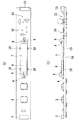
図10に、従来から用いられている高圧電源装置用の圧電トランス30の構成を示す。図10に示すように、圧電セラミックス振動体7に一次電極6、二次電極8が塗布されており、圧電セラミックス振動体7を収納するための圧電トランス・ケース25に一次入力端子29、二次出力端子27、GND端子28が装着されており、一次入力端子23からは一次リード線5により一次電極6に接続され、二次出力端子25からは二次リード線9により二次電極8に接続され、GND端子24からは圧電セラミックス振動体7のGND電極にリード線で接続されている。
FIG. 10 shows a configuration of a
このような圧電セラミックス振動体では、一次電極6とGNDとの間にその圧電トランスの共振周波数あるいはその近傍の周波数の交流電圧が印加すると、この圧電セラミックスに機械的振動が、図11では図の上下方向に、図10の上面図では紙面と垂直方向に、符号14の部分を節にした撓み振動として、生じる。このとき、GND電極と二次電極8との間に、交流高電圧が生じる。
In such a piezoelectric ceramic vibrator, when an AC voltage having a resonance frequency of the piezoelectric transformer or a frequency in the vicinity thereof is applied between the
圧電セラミックス振動体7は、駆動時(即ち振動時)に変位量の最も少ない箇所、これを節14とし、この節14の位置で、セラミックス振動体が、保持部材、言い換えれば、セラミック振動体そのものを図11に示す高圧回路基板に実装するため部材(図10においては、圧電トランス・ケース25)に接着固定されている。一次入力端子29、二次出力端子27、GND端子28の先端は、回路基板への孔明部に挿入して、印刷回路基板上の金属からなる導電部材(銅箔のパターン、あるいはランド)への半田付けが可能な突出した形状となっている。
The piezoelectric ceramic vibrating
図11は、図10に示した圧電トランス30を実装した、通常の高圧電源回路を構成する印刷回路基板16の側面図(断面図)の例を示す図である。図11において、入力コネクタ1は不図示の画像形成装置本体の制御ユニットに接続され、高圧出力のON/OFF並びに、高圧出力電圧値を設定する。回路基板16には低電圧制御回路2、圧電トランス30、整流回路10そして高圧出力電圧検出回路11が形成されており、出力コネクタ13から高圧電圧を出力する。
FIG. 11 is a diagram showing an example of a side view (cross-sectional view) of the printed
図10に示したような圧電トランスを高圧回路基板に実装するため部材(図10においては、圧電トランス・ケース25)については、圧電セラミックスのケースの形状及び実装構造に関して各種提案されている(たとえば、特許文献2、3参照)。
Various members (for example, the
しかしながら、上記のような従来例では以下のような欠点があった。すなわち、圧電セラミックス振動体を、外部接続用端子の形成された圧電セラミックス保持部材内に収納して圧電トランス・ユニットとして一体化し、この一体化した形状の圧電トランス・ユニットを回路基板に実装すると共に、圧電セラミックス振動体との間を、圧電セラミックス保持部材を介して電気接続することにより高圧電源装置を実現している。そのために、高圧電源装置は、圧電トランス・ユニットの大きさに制限されてしまい、さらなる小型化、薄型化、及び画像形成装置への最適配置が困難であるという問題点があった。 However, the conventional example as described above has the following drawbacks. That is, the piezoelectric ceramic vibrating body is housed in a piezoelectric ceramic holding member on which external connection terminals are formed and integrated as a piezoelectric transformer unit, and this integrated piezoelectric transformer unit is mounted on a circuit board. A high voltage power supply device is realized by electrically connecting the piezoelectric ceramic vibrating body through a piezoelectric ceramic holding member. For this reason, the high-voltage power supply device is limited by the size of the piezoelectric transformer unit, and there is a problem that it is difficult to further reduce the size and thickness and to optimally arrange the image forming device.
本発明は上記のような課題を解消するためになされたもので、その目的とするところは、圧電セラミックス振動体を用いた圧電トランスの安全性、出力性能を低下させることなく、画像形成装置への効率的最適配置をも可能となるさらなる小型化、薄型化を可能とした圧電トランスを用いた高圧電源装置を提供することにある。 The present invention has been made to solve the above-described problems, and an object of the present invention is to provide an image forming apparatus without deteriorating the safety and output performance of a piezoelectric transformer using a piezoelectric ceramic vibrator. It is an object of the present invention to provide a high-voltage power supply device using a piezoelectric transformer that can be further miniaturized and thinned.
上記目的を達成するため、本発明に係るプリント基板は、入力電圧が印加される1次側に1次電極とグランド電極が形成され、電圧が出力される2次側に2次電極が形成された圧電トランスを実装したプリント基板において、前記1次電極とリード線を介して接続された入力端子と、前記2次電極とリード線を介して接続された出力端子と、前記グランド電極が形成された面と対向する側に設けられた第1と第2の導電パターンと、前記第1導電パターンと電気的に接続され、且つ、固着されており、前記グランド電極と電気的に接続された第1端子と、前記第2導電パターンと固着されており、前記グランド電極が形成された面の前記2次側に設けられた第2端子とを備え、前記第1導電パターンと前記第1端子とが固着された第1位置と、前記第2導電パターンと前記第2端子とが固着された第2位置は、前記圧電トランスが振動した際の節部であることを特徴とする。 In order to achieve the above object, the printed circuit board according to the present invention has a primary electrode and a ground electrode formed on the primary side to which the input voltage is applied, and a secondary electrode formed on the secondary side to which the voltage is output. In the printed circuit board on which the piezoelectric transformer is mounted, an input terminal connected to the primary electrode via a lead wire, an output terminal connected to the secondary electrode via a lead wire, and the ground electrode are formed. First and second conductive patterns provided on the side opposite to the first surface, electrically connected to and fixed to the first conductive pattern, and electrically connected to the ground electrode. One terminal and a second terminal fixed to the second conductive pattern and provided on the secondary side of the surface on which the ground electrode is formed, the first conductive pattern and the first terminal And a first position where A second position where said second conductive pattern and the second terminal is fixed, the piezoelectric transformer is characterized in that it is a node portion when vibrated.
以上の構成によれば、高圧電源回路部を構成する電気部品を実装し、この部品間の接続を含み高圧電源回路部を形成するための長方形の構造体に、圧電トランスを、それを収容するケースを介さずに実装し、さらに高圧電源回路部を構成するそれぞれの回路の配置を、圧電トランスの実装位置あるいはその形状に対して、適切に配置することを可能とするので、電子写真方式の画像形成装置に使用する高圧電源装置として、その安全性、出力性能を含む各種性能を低下させることなく、小型化、薄型化することが可能になり、また画像形成装置への効率的最適配置をも可能とする。 According to the above configuration, the electrical components constituting the high-voltage power supply circuit unit are mounted, and the piezoelectric transformer is accommodated in the rectangular structure for forming the high-voltage power supply circuit unit including the connection between the components. Mounting without passing through the case, and the arrangement of each circuit constituting the high-voltage power supply circuit section can be appropriately arranged with respect to the mounting position of the piezoelectric transformer or its shape. As a high-voltage power supply device used for image forming devices, it can be reduced in size and thickness without degrading various performances including safety and output performance, and efficient and optimal arrangement for image forming devices can be achieved. Also possible.
以下、図面を参照して、本発明を各実施形態に基づいて説明する。
(第1の実施形態)
先ず、本発明による高圧電源装置を実装することが可能な装置の概要を図面に基づいて説明する。なお、図2から図11において、同じ符号は、全体を通して同じ構成要素を表している。
Hereinafter, with reference to the drawings, the present invention will be described based on each embodiment.
(First embodiment)
First, the outline | summary of the apparatus which can mount the high voltage power supply device by this invention is demonstrated based on drawing. 2 to 11, the same reference numerals denote the same components throughout.
図1は、本発明による高圧電源装置を実装することが可能な、レーザ・ビーム・プリンタ200の構成の概略を示す図である。レーザ・プリンタ200は記録紙Pを収納するデッキ201を有し、デッキ201から記録紙Pを繰り出すピックアップ・ローラ202、前記ピックアップ・ローラ202によって繰り出された記録紙Pを搬送するデッキ給紙ローラ対203、204が設けられている。
FIG. 1 is a diagram showing a schematic configuration of a
そして、記録紙Pを同期搬送するレジスト・ローラ対205が配設されている。また、レジスト・ローラ対の下流には、レーザ・スキャナ部206、207、208、209からのレーザ光に基づいてトナー像を感光ドラム210、211、212、213と、感光ドラムを均一な電位に帯電するための帯電ローラ230、231、232、233、潜像にトナーを載せ現像するための現像スリーブ234、235、236、237などを具備したプロセス・カートリッジが配設されており。
A
感光ドラム210、211、212、213上に形成されたトナー像を中間転写材218上に転写するためのローラ部材214、215、216、217(以後一次転写ローラと記す)、中間転写材218上に形成された画像を記録紙Pに転写する転写ローラ219部材(以後二次転写ローラ)が二次転写ユニット駆動カム221にて駆動される二次転写ユニット220に配設されている。さらに記録紙Pの電荷を除去し、中間転写材218からの記録紙の分離を促進するための放電部材222(以後除電針と記す)が配設されている。帯電ローラ230、231、232、233、現像スリーブ234、235、236、237、転写のためのローラ部材214、215、216、217、及び、中間転写材218上に形成された画像を記録紙Pに転写する転写ローラ219には、高圧電源装置238から高圧バイアスを印加する構成になっている。
さらに、除電針222の下流に記録紙P上に転写されたトナー像を熱定着するために内部に加熱用のハロゲン・ヒータ223を備えた定着ローラ224と加圧ローラ225対、定着ローラ224と加圧ローラ223対の下流には、記録紙を排紙する排紙ローラ対226、227が配設されている。
Further, in order to thermally fix the toner image transferred onto the recording paper P downstream of the
次に、本発明を適用することが可能な高圧電源装置の電気回路の例を説明する。
図2(a)は、本発明の形態に係る高圧電源装置の代表的な構成を示すブロック図であり、同図中、符号1は、不図示の画像形成装置本体の制御回路からの制御信号を受ける入力コネクタであり、符号7は圧電セラミックス振動体である。圧電セラミックス振動体7の出力は、ダイオード105、106、及びコンデンサ107から構成される高圧整流回路10にて整流平滑され、出力コネクタ13から出力され、負荷に接続される。この高圧整流回路の出力端(即ち、ダイオード106のカソード側)は抵抗108、109から成る高圧検出回路11にも接続される。高圧出力Edc(V)は、抵抗108、109により分圧され、抵抗110を介してオペ・アンプ113の反転入力端子(−)に接続される。このとき、オペ・アンプ113の反転入力端子(−)に発生する電圧Vsns(V)は、
Vsns = Edc*R109/(R108+R109) (式1)
で表される。またオペ・アンプ113の非反転端子(+)は不図示の画像形成装置本体の制御回路からの制御信号を入力する。オペ・アンプ112の出力端は電圧制御発振器(VCO)101に接続され、この電圧制御発振器101の出力端は、電界効果トランジスタ(以下FET)102のゲートに接続される。FET102のドレインはインダクタ103を介して電源に接続されると同時に圧電トランス7の一次側電極に接続される。一次電極の他端はGND電極として接地される。
Next, an example of an electric circuit of a high voltage power supply device to which the present invention can be applied will be described.
FIG. 2A is a block diagram showing a typical configuration of a high-voltage power supply device according to an embodiment of the present invention. In FIG. 2,
Vsns = Edc * R109 / (R108 + R109) (Formula 1)
It is represented by The non-inverting terminal (+) of the
図2(b)は、圧電セラミックス振動体7の駆動信号の周波数に対する出力電圧の特性を示したものである。図に示すように、出力電圧は、駆動信号の周波数によって変化し、共振周波数f0において出力電圧が最大となり、この共振周波数の前後の周波数では、共振周波数との差に比例するかたちで、出力電圧が低下する。したがって、駆動周波数を変化させることで出力電圧の制御が可能であることがわかる。規定出力電圧Edc出力時に、駆動周波数はfxである。出力電圧Edcが上がると、オペ・アンプ103の電圧Vsnsが上がり、オペ・アンプ103の出力端子の電圧は下がる。このとき、電圧制御発振器101は入力電圧が下がると出力周波数が上がるような動作を行うものとすると、圧電セラミックス振動体7の駆動周波数が上がる。したがって共振周波数fxより少し高い周波数で圧電セラミックス振動体7は駆動される。圧電セラミックス振動体7の駆動周波数が上がると出力電圧は下がるよう制御される。
FIG. 2B shows the characteristics of the output voltage with respect to the frequency of the drive signal of the piezoelectric
また、出力電圧Edcが下がった場合には、オペ・アンプ103の電圧Vsnsが下がり、オペ・アンプ103の出力端子電圧は上昇する。
When the output voltage Edc decreases, the voltage Vsns of the
このとき、電圧制御発振器101は入力電圧が上がると出力周波数が下がるような動作を行うものとすると、圧電セラミックス振動体7の駆動周波数が下がる。したがって共振周波数fxより少し低い周波数で圧電セラミックス振動体7は駆動される。圧電セラミックス振動体7の駆動周波数が低がると出力電圧は上がるよう制御される。
よって、このVCOへの帰還ループは、フィードバック・ループを形成し、オペ・アンプ113の(+)端子に入力される画像形成装置本体の制御回路からの制御信号電圧と高圧検出回路11の分圧出力電圧が等しくなるように、出力電圧が定電圧制御されることになる。
At this time, if the voltage controlled
Therefore, this feedback loop to the VCO forms a feedback loop, and the control signal voltage from the control circuit of the image forming apparatus main body input to the (+) terminal of the
以上の説明は、高圧の出力電圧を所望の電圧に制御する場合である。感光ドラムは均一に帯電処理される必要があり、この際に、負荷電流量を制御することも通常行われている。高圧電流値の所定の値に制御する場合は、たとえば、図2(a)のダイオード105と直列接続される抵抗の両端電圧(を平滑した電圧)を画像形成装置本体の制御回路が入力して、その結果をオペ・アンプ113の(+)端子に加える電圧に反映させることによっても、あるいは、高圧検出回路11からの信号に代えて、前述したダイオード105と直列接続される抵抗の電圧を、オペ・アンプ113の(−)端子に加えることによっても、実行することが可能である。また、GNDに戻る負荷電流を、抵抗を経由するように構成し、その両端電圧を帰還させるようにしてもよい。
The above description is a case where the high voltage output voltage is controlled to a desired voltage. The photosensitive drum needs to be uniformly charged, and at this time, the load current amount is usually controlled. When controlling to a predetermined value of the high voltage current value, for example, the control circuit of the main body of the image forming apparatus inputs the voltage across the resistor connected in series with the
図2(a)において、抵抗110、111、オペ・アンプ113、コンデンサ112、VCO101、FET102、コイル103を含む回路は、整流回路10、あるいは高圧検出回路11が高圧回路であるのに対して、低電圧制御回路を構成する。
In FIG. 2A, the circuit including the
これまでの説明では、高圧電源装置の電気的回路の構成の説明を主にしていた。以下、本発明に係わる高圧電源装置の構造について図3から図9を用いて、それぞれの実施形態について詳細に説明を進める。 The description so far has mainly described the configuration of the electrical circuit of the high-voltage power supply device. Hereinafter, the structure of the high-voltage power supply device according to the present invention will be described in detail for each embodiment with reference to FIGS.
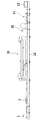
図3は、図2に例示したような動作を行う圧電トランスを用いた高圧電源装置の物理的構造の第1の実施形態を示した図であり、その構造の上面図と側方からの断面図を示した図である。ここで、構造体12は、上方に開口部を有する箱形状のものであり、その内部に圧電セラミックス振動体7を収容する。図示するように、この構造体12は、セラミック振動体の長辺方向に長く、セラミック振動体の短辺方向に短い形状を有している。この構造体の場合、上面から見たそれぞれの辺の寸法は、使用するセラミック振動体のそれぞれの辺の2倍以下の寸法で、電子写真方式を用いた画像形成装置の高圧電源装置(たとえば、図2に示した高圧電源装置)を構成することが可能である。この図では、構造体12が、この圧電セラミックス振動体に関連する電気回路、すなわち高圧電源装置を構成する電気回路部品を、箱形状の内部底面と、この内部底面に対向する外部底面と、に分けて実装することを示そうとしている。一次電極6と二次電極8が形成された圧電セラミックス振動体7を、その機械的変位量の最も少ない節箇所で、構造体12の内部底面の突出部14に、固着している。
FIG. 3 is a diagram showing a first embodiment of a physical structure of a high-voltage power supply device using a piezoelectric transformer that performs the operation illustrated in FIG. 2, and a top view of the structure and a cross section from the side. It is the figure which showed the figure. Here, the
圧電セラミックス振動体7の一次電極6は、一次電極リード線5及び一次入力端子4により、構造体12の裏面(外部底面:開口部を上方とした場合の容器の底面で、図面上で下側の面を言う)に実装されている低電圧制御回路2の出力ラインに接続されている。また画像形成装置本体の制御回路との間の、VCC、GND及び端子1(コントローラ)の接続は、構造体12に実装されている入力コネクタ1により行われる。
The
圧電セラミックス振動体7の一次電極6の他方は、GND電極として、構造体12の圧電セラミック振動体側の面(内部底面)上に設けられた電極とリード線を介して接続され、最終的に構造体12の裏面(外部底面)に実装されている低電圧制御回路2のGNDに接続される。
The other
二次電極8は、二次電極リード線9により、構造体上12の圧電セラミック振動体側の面(内部底面)に実装されている高圧整流回路10に接続され、この高圧整流回路10は電圧検出回路11に接続されている。この高圧電源装置の出力は高圧出力端子13により画像形成装置本体の負荷に接続される。圧電セラミックス振動体7は、構造体12によって、その周囲が被われるように囲まれている。
The
一次電極6に接続される低電圧制御回路2、二次電極8に接続される高圧整流回路10、電圧検出回路11等を構成する電気回路部品は、構造体12に形成された配線(導電)パターン(ランド)等を介して実装され、それぞれの部品間も表面に形成された配線(導電)パターンによって、接続される。
The electrical circuit components constituting the low
一次電極6に接続される低電圧制御回路2は、構造体12の外部底面、すなわち、セラミック振動対の一次電極6の近傍で、構造体12の裏面側に実装される。すなわち、その部分に配線パターン(ランド)を形成し、低電圧制御回路2を構成する部品を実装することで、低電圧制御回路を形成している。二次電極8に接続される高圧整流回路10、電圧検出回路11等の電気回路部品は、構造体の外部底面と対向する内部の底面、すなわち、圧電セラミックス振動体が収容される開口部側の面上で、圧電セラミック振動対の二次電極とこの構造体の端部との間の面(内部底面)に、配線パターンを形成し部品を実装することで回路を形成している。
The low
このような、立体的な構造体上に配線パターンを構成する技術は、MID(Molded Interconnection Device)射出成形法(以下、MID法と略す)と呼ばれ、射出成形等から得られた成形品に、所定の方法で電気回路(メッキ配線等)を形成する方法であり、近年、配線パターン成形方法にレーザ加工を用いるなどさまざまな方法が提案されている。MID法によって製作された部材はMIDと呼ばれ、MID法によって3次元立体配線をすることで電気部品の立体的な配置が可能となり、また、射出成型品のために形状精度を出しやすく、小型化が容易となり、高密度実装が可能となる特徴がある。 Such a technique for forming a wiring pattern on a three-dimensional structure is called a MID (Molded Interconnection Device) injection molding method (hereinafter abbreviated as MID method), and is used for a molded product obtained by injection molding or the like. In this method, an electric circuit (plated wiring or the like) is formed by a predetermined method. In recent years, various methods such as using laser processing as a wiring pattern forming method have been proposed. A member manufactured by the MID method is called MID, and three-dimensional solid wiring is possible by the MID method, so that three-dimensional arrangement of electrical parts is possible, and it is easy to obtain shape accuracy for injection molded products, and is compact. This makes it easy to achieve high-density mounting.
このように圧電トランスの技術とMID法に代表される技術を用い、機構部品即ち圧電セラミックス振動体、低電圧制御回路部、高電圧回路部(高圧整流回路10、電圧検出回路:11)の実装配置を、図示するような長方形の形状の構造体の面上に、物理的に(その間の寸法および実装面を、耐圧および放電・漏れ電流等を考慮して、違えることによって)分離して形成することによって、形状の自由度が高く小型が可能な高圧電源装置を提供することが可能となる。また、高圧電源装置の形状自由度が高くかつ小型化できることによって、画像形成装置本体への実装自由度が増し、画像形成装置の小型化、低廉化、高性能化に寄与できる。また、小型化によって、高圧電圧を必要とする部分のそれぞれの近傍に独立に配置することが可能になり、したがって高圧電圧を配線によって引き回すことを回避することが可能になり、このことはそれまでの各種の対策を不要にすることを、あるいは機能縮小することを可能にする。
As described above, using the technology of the piezoelectric transformer and the technology represented by the MID method, mounting of the mechanical parts, that is, the piezoelectric ceramic vibrator, the low voltage control circuit unit, and the high voltage circuit unit (the high
本実施形態を説明する図では出力端子をファストン・タブ形状として記載してある。しかしながら、この形状についてはファストン・タブ形状に限定したものではなく、画像形成値の接点形状にあわせた形状とすることも、さらに、構造体12で出力端子部の周囲を囲み、画像形成装置に装着した際の他ユニットとの絶縁距離を保つ構成とすることも可能である。
In the drawings for explaining the present embodiment, the output terminals are described as faston tab shapes. However, this shape is not limited to the Faston tab shape, but may be a shape that matches the contact shape of the image forming value. Further, the
また、画像形成装置の説明を、タンデム方式のカラー画像形成装置を例に説明しているが、高圧バイアスを用いた画像形成装置についても本発明を適用して、上述したような各種の利点を得ることができる。 Further, the description of the image forming apparatus has been described by taking a tandem color image forming apparatus as an example. However, the present invention can be applied to an image forming apparatus using a high voltage bias, and various advantages as described above can be obtained. Obtainable.
(第2の実施形態)
図4、図5は、本発明に係わる第2の実施形態の例を説明する図である。上述した第1の実施形態との主たる相違点は、上述した構造体として、通常の印刷回路基板を使用していることである。また、次の相違点としては、圧電セラミックス振動体および構造体(印刷回路基板)に、固着するため処理を施していることである。さらなる相違点は、低電圧制御回路2の主要電気部品を印刷回路基板のいわゆる部品面に、言い換えれば、圧電セラミックス振動体を実装する側の面に配置したことであり、これに応じて、構造体16(印刷回路基板)は、第1の実施形態に較べて、圧電セラミックス振動体の一次電極側に延長されている。
(Second Embodiment)
4 and 5 are diagrams for explaining an example of the second embodiment according to the present invention. The main difference from the first embodiment described above is that a normal printed circuit board is used as the structure described above. Further, the next difference is that the piezoelectric ceramic vibrating body and the structure (printed circuit board) are processed to adhere to each other. A further difference is that the main electrical components of the low-
ここで、図4は、たとえば図2に示した高圧電源装置を実装した回路基板の上面図とその側面図を示し、図5は、図4の側面の一部を拡大して説明するための図である。図4及び図5を基に、本発明に係わる第2の実施形態について説明を進める。 4 shows a top view and a side view of a circuit board on which, for example, the high-voltage power supply device shown in FIG. 2 is mounted, and FIG. 5 is an enlarged view of a part of the side surface of FIG. FIG. The second embodiment according to the present invention will be described based on FIG. 4 and FIG.
図中、圧電セラミックス振動体7には、一次電極6、二次電極8、に加え節14の部分に固着用を兼ねた金属からなる端子17(図5)を設けている。図15に示した部分の端子17は、一次電極6に対向するGND電極18と電気的に接続されている。また、この端子17は、二次電極側にも形成されており、計4個の端子が圧電セラミックス振動体の上面から見た場合の側面部に形成されている。ただし、二次電極側に設けられる端子は、単に固着のためだけの端子である。この部分は、図4の上面図で圧電セラミックス振動体の周辺部の符号15に対応する位置である。
In the figure, the piezoelectric ceramic vibrating
圧電セラミックス振動体の一次電極6は一次電極リード線5により、印刷回路基板のいわゆる部品面およびパターン面にその構成部品が実装された低電圧制御回路2に接続されている。また、画像形成装置本体の制御回路との間の、VCC、GNDおよび端子1(コントローラ)の接続は、入力コネクタ1により行われる。
The
圧電セラミックス振動体の一次電極6の他方(符号18)は、GND電極として、圧電セラミック振動体7上で、図5に示す部分の端子17と接続され、この端子7は、対応する位置にあるパターン(ランド)を介して低電圧制御回路2のGND回路と電気的に接続されている。圧電セラミックス振動体の二次電極8は、二次電極リード線により、高圧整流回路10に接続され、高圧整流回路10は電圧検出回路11に接続されている。この高圧電源装置の出力は高圧出力端子13を介して画像形成装置本体の負荷に接続される。
The other primary electrode 6 (symbol 18) of the piezoelectric ceramic vibrator is connected as a GND electrode to the
圧電セラミックス振動体7と印刷回路基板16への固定(固着)方法に関して、図5に基づいて説明を進める。圧電セラミックス振動体7上の端子17は、一次、二次電極と同様に、銀(Ag)等にて形成される。この端子17は、圧電セラミックス振動体7の機械的変位量の最も少ない節の箇所に設けられており、これらの電極厚み19は約15μmである。一方圧電セラミックス振動体が固着される印刷回路基板には、圧電セラミックスを固着するための導電パターン(ランド)15を形成する。通常、印刷回路基板の配線導体パターンのパターン厚み20は35μmである。印刷回路基板の金属からなる配線導体にて形成された圧電セラミックス保持パターン15と、圧電セラミックス振動体7に形成された金属からなる端子17を半田付けすることにより、圧電セラミック振動体7は回路基板16に固着され、固定されることになる。
The method for fixing (fixing) the piezoelectric
なお、図5における圧電セラミックス振動体の位置は、一次電極の位置であり、その部分の端子17は及びパターン(ランド)15は、一次電極のGND電極と印刷回路基板側のGNDとの電気的接続をすると同時に、圧電セラミックス振動体と印刷回路基板との間の固着をする部分であり、図5に示されていない二次電極側の端子17とパターン(ランド)15との間の半田付けは単に相互の固着のみの役割を有し、電気的な接続は意味を持たない。 Note that the position of the piezoelectric ceramic vibrating body in FIG. 5 is the position of the primary electrode, and the terminal 17 and the pattern (land) 15 of that portion are the electrical connection between the GND electrode of the primary electrode and the GND on the printed circuit board side. At the same time as the connection, the piezoelectric ceramic vibrating body and the printed circuit board are fixed to each other, and soldering between the terminal 17 on the secondary electrode side and the pattern (land) 15 not shown in FIG. Only has a role of mutual fixation, and the electrical connection has no meaning.
圧電セラミックス振動体の振動時の変位量(振幅)は、最大で1μm程度であるため、印刷回路基板の配線導体パターン厚みにて確保された空間にて、充分な機械振動が可能となるために、図5に示す固着手法を使用しても、圧電トランスとしての性能を損なうことはない。 Since the displacement (amplitude) of the piezoelectric ceramic vibrating body during vibration is about 1 μm at the maximum, sufficient mechanical vibration is possible in the space secured by the wiring conductor pattern thickness of the printed circuit board. Even if the fixing method shown in FIG. 5 is used, the performance as a piezoelectric transformer is not impaired.
低電圧制御回路2は、圧電セラミックス振動体7の一次電極6側の回路基板16上に形成されている金属からなる配線パターン(ランド)に回路部品を半田付けすることにより形成されている。図4においては、高圧電源装置を構成する主要電気部品を圧電セラミックス振動体と同一面に配置した形状としているが、圧電セラミックス振動体7の配置面ではない面に配置すること、さらには、上述した第1の実施形態のように、圧電セラミックス振動体7を実装する面の裏面に位置する箇所に、低電圧制御回路2を配置することも可能である。図4の側面図には、低電圧制御回路2を構成する寸法の小さな電気部品を裏面、すなわちパターン面に実装した構成を示している。
The low
このように、圧電セラミックス振動体7に固着用の金属からなる端子17を設け、回路基板上に圧電セラミックスを固着するための金属からなるパターン(ランド)15を設け、両者を半田付けすることにより、樹脂等で形成されていたケースとしての保持部材、すなわち圧電セラミックス振動体を印刷回路基板に実装するための部材の必要がなくなるために、より薄型の高圧電源装置の提供が可能となる。また、図に示したように、圧電セラミックス振動体を実装する印刷回路基板の形状を、圧電セラミックス振動体の形状に似せて、長方形状に形成し、高圧回路と定圧回路とを、圧電セラミックスの実装部分によって分離するように実装することによって電位差を生じる部品あるいはパターン間の距離を大きく取ることが可能になり、高圧電圧を安定した形で、供給することが可能になる。また、本発明に係わる印刷回路基板は、図4に示したように、圧電セラミックス振動体の長辺の近傍には、電気部品を実装することはしていない。また、図示していないが、印刷回路基板の部品面で、圧電セラミックス振動体に面する部分は、パターンを設けていない。高圧整流部10および電圧検出回路のGNDラインと低電圧制御回路のGNDラインとの間を接続するパターンは、裏面に相当するパターン面上に構成している。
In this way, the piezoelectric ceramic vibrating
(第3の実施形態)
図6、図7は第3の実施形態の例を説明する図である。第1の実施形態の例との主たる相違点は、上述した構造体として、通常の印刷回路基板としていることであり、第2の実施形態の例との相違点は、圧電セラミックス振動体7の印刷回路基板への固着(固定)方法が、回路基板16の回路構成部品(チップ部品)の実装時に使用されるチップ部品接着剤を使用して行われることである。したがって、第2の実施形態では必要であった、圧電セラミックス振動体上の端子17および対応する印刷回路基板側のランド15は、あってもかまわないが、基本的は不要である。言い換えれば、圧電セラミックス振動体としては、第1の実施形態における圧電セラミックス振動体を使用することができる。その他は、第2の実施形態と何ら変わるところはない。
(Third embodiment)
6 and 7 are diagrams for explaining an example of the third embodiment. The main difference from the example of the first embodiment is that the above-described structure is a normal printed circuit board. The difference from the example of the second embodiment is that the piezoelectric ceramic vibrating
図6及び図7を基に、第3の実施形態について説明を進める。図中、圧電セラミックス振動体7には、一次電極6、二次電極8、およびGND電極のみが設けられ、一次電極6は一次電極リード線5により、低電圧制御回路2に接続されている。また画像形成装置本体の制御回路との接続は、入力コネクタ1により行われる。
Based on FIG.6 and FIG.7, description is advanced about 3rd Embodiment. In the figure, the piezoelectric
一次電極6の他方は、GND電極として、図示していないが、リード線あるいは他の何らかの圧電セラミックス振動体の振動を妨げない方法で、低電圧制御回路2のGND回路と接続されている。二次電極8は二次電極リード線により、高圧整流回路10に接続され、高圧整流回路10は電圧検出回路11に接続されている。この高圧電源装置の出力は高圧出力端子13により画像形成装置本体の負荷に接続される。
The other of the
圧電セラミックス振動体7と回路基板16への固定(保持)方法に関して図7に基づいて説明を進める。
The method for fixing (holding) the piezoelectric ceramic vibrating
圧電セラミックス振動体7の機械的変位量の最も少ない節の箇所をチップ部品接着剤にて接着する。この接着部分を図6の上面図における、圧電セラミックス振動体の周囲の黒丸部分で示す。圧電セラミックスの電極厚み19は約15μmである。圧電セラミックス振動体の保持部材と成る回路基板と圧電セラミックス振動体7との間隔は、固化したチップ部品接着剤の厚みで確保される。通常、回路基板に使用されるチップ部品接着剤の厚み22はチップ部品実装時に調整することが可能であり、圧電セラミックス振動体7のチップ部品接着剤による印刷回路基板への固着においては、実装固定後に30〜50μmの範囲の間隔が維持されるように取付られるよう調整される。このようにチップ部品接着剤21を使用することによって、圧電セラミックス振動体7を特別な部材を用いることなく、所定の間隔を維持しながらも印刷回路基板に固着(固定)することができる。このチップ部品接着剤により確保された回路基板との間隔によって、圧電セラミックス振動体の振動時の変位量(振幅)は確保され、圧電トランスとしての性能を損なうことがない。
The portion of the node having the smallest mechanical displacement of the piezoelectric ceramic vibrating
低電圧制御回路2は、圧電セラミックス振動体7の一次電極6側の回路基板16上に形成されている金属からなる配線パターンに回路部品を半田付けすることにより形成されている。図6において低電圧制御回路2は、圧電セラミックス振動体と同一面に配置した形状としているが、圧電セラミックス振動体7の配置面(部品面)ではない面に配置すること、さらには、圧電セラミックス振動体7の裏面に位置する箇所に配置することも可能である。
The low
このように、圧電セラミックス振動体7をチップ部品接着剤21で、印刷回路基板上に固着(固定)することにより、従来においては樹脂等で形成されていたケースとしての保持部材の必要がなくなるために、より薄型の高圧電源装置の提供が可能となる。また、この方法は、圧電セラミックス振動体と印刷回路基板の双方に固着のための配慮、たとえば端子17やパターン(ランド)15を基本的には必要としないため、印刷基板の寸法が許す限り、異なる大きさの圧電セラミックス振動体を使用することができる特徴を有する。
In this way, by fixing (fixing) the piezoelectric ceramic vibrating
(第4の実施形態)
図8、図9は第4の実施形態を説明する図である。第4の実施形態の主たる特徴は、上述した構造体として通常の印刷回路基板を使用し、圧電セラミックス振動体を実装する位置に、その圧電セラミックス振動体7の外形よりも大きなスリットを印刷回路基板に設けると共に、この回路基板のスリット内側部分に突出部を形成し、この突出部と圧電セラミックス振動体の機械的変位量の最も少ない節の部分を固定することである。
(Fourth embodiment)
8 and 9 are diagrams for explaining the fourth embodiment. The main feature of the fourth embodiment is that an ordinary printed circuit board is used as the structure described above, and a slit larger than the outer shape of the piezoelectric
図8、図9を用いて、第4の実施形態について説明する。なお第1から第3の実施形態と重複する箇所は省略する。 The fourth embodiment will be described with reference to FIGS. In addition, the part which overlaps with 1st-3rd embodiment is abbreviate | omitted.
印刷回路基板16に、圧電セラミックス振動体7の外形よりも大きなスリット24を設け、スリット24内に、突出部23を設ける。この突出部23は、圧電セラミックス振動体7の機械的変位量の最も少ない節の位置に対応した位置であり、図8の上面図に示す通り4箇所に設ける。
A slit 24 larger than the outer shape of the piezoelectric ceramic vibrating
圧電セラミックス振動体7の節箇所と回路基板16の突出部23は、チップ部品接着剤21で固着(固定)される。この場合、第2あるいは第3の実施形態のように、圧電セラミックス振動体と印刷回路基板との間の間隔については考慮する必要がない。また双方を固着(固定)する方法は、第2の実施形態で示した方法(半田付け)を用いたものでもよい。この場合、上述したように、圧電セラミックス振動体と印刷回路基板の双方に第2の実施形態で示した処置が必要になる。
The node portion of the piezoelectric ceramic vibrating
このように、回路基板16にスリットを設けることにより第2および第3の実施形態で示した高圧電源装置の小型化の可能性に加え、圧電セラミックス振動体裏面空間が大きくできるために、製造時の取り扱いが簡単となる効果が得られる。また、圧電セラミックス振動体裏面空間が大きくできるために、印刷回路基板のそり(湾曲)を無視することができる特徴がある。
Thus, by providing a slit in the
以上の第1の実施形態例1から第4の実施形態において説明した電気回路の構成については、本発明を説明する上での最小構成を示すものであり、高圧電源装置が実装される装置に対応して高圧電源装置に求められることになる各種の機能を含む電気回路を、本発明を使用して実装することが容易にできることは当業者には明らかであろう。 The configuration of the electric circuit described in the first to fourth embodiments is a minimum configuration for explaining the present invention, and is applied to a device on which the high-voltage power supply device is mounted. It will be apparent to those skilled in the art that an electrical circuit including various functions that would be required for a high-voltage power supply device can be easily implemented using the present invention.
1 入力コネクタ
2 低電圧制御回路
3 GND端子
4 一次入力端子
5 一次リード線
6 一次電極
7 圧電セラミックス振動体
8 二次電極
9 二次リード線
10 高圧整流回路
11 電圧検出回路
12 MID(構造体、電気回路基板)
13 高圧(二次)出力端子
14 セラミック振動体保持用突起
15 圧電セラミックス保持用の導電パターン(ランド)
16 構造体(回路基板)
17 圧電セラミックス上に形成された固着用を兼ねた端子
18 GND電極
19 電極厚み
20 回路パターン厚み
21 チップ部品接着剤
22 チップ部品接着剤厚み
23 構造体(回路基板)突出部(固着部)
24 構造体のスリット(切り欠き)部
25 圧電トランス・ケース
27 二次出力端子
28 GND端子
29 一次入力端子
30 圧電トランス
101 VCO
102 FET
103 コイル
105、106 ダイオード
108、109、110、111 抵抗
112 コンデンサ
113 OPアンプ
200 画像形成装置
201 デッキ
202 ピックアップ・ローラ
203、204 給紙ローラ
205 レジスト・ローラ
206、207、208、209 レーザ・スキャナ
210、211、212、213 感光ドラム
214、215、216、217 一次転写ローラ
218 中間転写材
219 二次転写ローラ
220 二次転写ユニット
221 二次転写ユニットカム
222 除電針
223 ハロゲン・ヒータ
224 定着ローラ
225 加圧ローラ
226、227 排紙ローラ
230、231、232、233 帯電ローラ
234、235、236、237 現像スリーブ
238 高圧電源装置
DESCRIPTION OF
13 High Voltage (Secondary)
16 Structure (circuit board)
17 Terminals that are also used for fixing formed on
24 Structure Slit (Notch) 25
102 FET
103
Claims (2)
前記1次電極とリード線を介して接続された入力端子と、An input terminal connected to the primary electrode via a lead wire;
前記2次電極とリード線を介して接続された出力端子と、An output terminal connected to the secondary electrode via a lead wire;
前記グランド電極が形成された面と対向する側に設けられた第1と第2の導電パターンと、First and second conductive patterns provided on the side facing the surface on which the ground electrode is formed;
前記第1導電パターンと電気的に接続され、且つ、固着されており、前記グランド電極と電気的に接続された第1端子と、A first terminal electrically connected to and fixed to the first conductive pattern, and electrically connected to the ground electrode;
前記第2導電パターンと固着されており、前記グランド電極が形成された面の前記2次側に設けられた第2端子とを備え、A second terminal that is fixed to the second conductive pattern and provided on the secondary side of the surface on which the ground electrode is formed;
前記第1導電パターンと前記第1端子とが固着された第1位置と、前記第2導電パターンと前記第2端子とが固着された第2位置は、前記圧電トランスが振動した際の節部であることを特徴とするプリント基板。The first position where the first conductive pattern and the first terminal are fixed and the second position where the second conductive pattern and the second terminal are fixed are the nodes when the piezoelectric transformer vibrates. A printed circuit board characterized by
前記第1端子と対向する位置に1対の第1突出部と、A pair of first protrusions at positions facing the first terminals;
前記第2端子と対向する位置に1対の第2突出部と、を備え、A pair of second protrusions at a position facing the second terminal,
前記第1突出部に前記第1の導電パターンが設けられ、前記第2突出部に前記第2の導電パターンが設けられたことを特徴とする請求項1に記載のプリント基板。The printed circuit board according to claim 1, wherein the first conductive pattern is provided on the first projecting portion, and the second conductive pattern is provided on the second projecting portion.
Priority Applications (1)
| Application Number | Priority Date | Filing Date | Title |
|---|---|---|---|
| JP2004237593A JP4926388B2 (en) | 2004-08-17 | 2004-08-17 | High voltage power supply used for image forming apparatus |
Applications Claiming Priority (1)
| Application Number | Priority Date | Filing Date | Title |
|---|---|---|---|
| JP2004237593A JP4926388B2 (en) | 2004-08-17 | 2004-08-17 | High voltage power supply used for image forming apparatus |
Publications (3)
| Publication Number | Publication Date |
|---|---|
| JP2006059875A JP2006059875A (en) | 2006-03-02 |
| JP2006059875A5 JP2006059875A5 (en) | 2010-04-02 |
| JP4926388B2 true JP4926388B2 (en) | 2012-05-09 |
Family
ID=36107118
Family Applications (1)
| Application Number | Title | Priority Date | Filing Date |
|---|---|---|---|
| JP2004237593A Expired - Fee Related JP4926388B2 (en) | 2004-08-17 | 2004-08-17 | High voltage power supply used for image forming apparatus |
Country Status (1)
| Country | Link |
|---|---|
| JP (1) | JP4926388B2 (en) |
Families Citing this family (5)
| Publication number | Priority date | Publication date | Assignee | Title |
|---|---|---|---|---|
| JP4944632B2 (en) * | 2007-02-05 | 2012-06-06 | キヤノン株式会社 | Circuit board, high voltage power supply device and image forming apparatus |
| KR101238373B1 (en) | 2008-07-24 | 2013-02-28 | 삼성전자주식회사 | Apparatus for supplying high voltage power |
| JP2013175556A (en) * | 2012-02-24 | 2013-09-05 | Yokogawa Electric Corp | Piezoelectric transformer and mounting method of the same |
| JP5893675B2 (en) * | 2013-06-03 | 2016-03-23 | 株式会社タムラ製作所 | Electronic component module |
| US10671009B2 (en) | 2017-02-13 | 2020-06-02 | Canon Kabushiki Kaisha | Printed circuit board mounting piezoelectric transformer |
Family Cites Families (8)
| Publication number | Priority date | Publication date | Assignee | Title |
|---|---|---|---|---|
| JPH04127486A (en) * | 1990-09-18 | 1992-04-28 | Fujitsu Ltd | Piezoelectric transformer |
| JPH0964432A (en) * | 1995-08-24 | 1997-03-07 | Sony Corp | Piezoelectric ceramic transformer |
| JP2927235B2 (en) * | 1996-04-04 | 1999-07-28 | リコー計器株式会社 | Electrode connection structure of piezoelectric transformer |
| JP3085233B2 (en) * | 1997-02-26 | 2000-09-04 | 株式会社村田製作所 | Piezoelectric transformer |
| JP4344023B2 (en) * | 1998-06-05 | 2009-10-14 | Necトーキン株式会社 | Mounting structure of piezoelectric transformer element and manufacturing method of piezoelectric transformer |
| JP3185976B2 (en) * | 1998-07-15 | 2001-07-11 | 日本電気株式会社 | Piezoelectric transformer |
| JP2002064977A (en) * | 2000-08-21 | 2002-02-28 | Matsushita Electric Ind Co Ltd | Method of driving pezoelectric transformer and power supply |
| JP2002190626A (en) * | 2000-12-20 | 2002-07-05 | Sharp Corp | Power supply circuit |
-
2004
- 2004-08-17 JP JP2004237593A patent/JP4926388B2/en not_active Expired - Fee Related
Also Published As
| Publication number | Publication date |
|---|---|
| JP2006059875A (en) | 2006-03-02 |
Similar Documents
| Publication | Publication Date | Title |
|---|---|---|
| RU2317630C2 (en) | Power supply and image shaping device incorporating such power supply | |
| US8549742B2 (en) | High-voltage power supply device and image forming apparatus having same | |
| JP4721431B2 (en) | Power supply, image forming apparatus and IC | |
| US11307525B2 (en) | Printed circuit board mounting piezoelectric transformer | |
| JP4926388B2 (en) | High voltage power supply used for image forming apparatus | |
| US10705476B2 (en) | Plurality of boards mounted on image forming apparatus | |
| US8487475B2 (en) | Power supply apparatus and method of supplying power | |
| JP2003195594A (en) | Image recorder | |
| JP4944632B2 (en) | Circuit board, high voltage power supply device and image forming apparatus | |
| JP5340255B2 (en) | Power supply, IC and image forming apparatus | |
| JP2006158033A (en) | High-voltage power supply used for image forming apparatus | |
| JP7362422B2 (en) | Power supply device and image forming device | |
| JP2009109554A (en) | Image forming apparatus | |
| JP7301600B2 (en) | Power supply and image forming apparatus | |
| JP2006129673A (en) | High voltage power supply device and method of controlling high voltage power supply device | |
| JP6882906B2 (en) | Printed circuit board, power supply and image forming equipment | |
| JP2009171832A (en) | High-tension power supply, image forming device having the same, and circuit board of the same | |
| JP6882907B2 (en) | Electronic component mounting method, printed circuit board, power supply device and image forming device | |
| JP2008147301A (en) | Piezoelectric transformer high-voltage power supply | |
| JP4054735B2 (en) | Image recording device | |
| JP2008191387A (en) | Image recorder | |
| JP2019160873A (en) | Piezoelectric element, piezoelectric transformer, piezoelectric transformer device, and electronic device | |
| JP2008148506A (en) | Power supply device and image forming device with same | |
| JP4366343B2 (en) | High voltage power supply device using piezoelectric transformer and image forming apparatus using the same | |
| JP2008042982A (en) | Piezoelectric transformer high voltage power supply |
Legal Events
| Date | Code | Title | Description |
|---|---|---|---|
| A621 | Written request for application examination |
Free format text: JAPANESE INTERMEDIATE CODE: A621 Effective date: 20070803 |
|
| A521 | Request for written amendment filed |
Free format text: JAPANESE INTERMEDIATE CODE: A523 Effective date: 20100212 |
|
| RD02 | Notification of acceptance of power of attorney |
Free format text: JAPANESE INTERMEDIATE CODE: A7422 Effective date: 20101106 |
|
| A977 | Report on retrieval |
Free format text: JAPANESE INTERMEDIATE CODE: A971007 Effective date: 20110414 |
|
| A131 | Notification of reasons for refusal |
Free format text: JAPANESE INTERMEDIATE CODE: A131 Effective date: 20110422 |
|
| A521 | Request for written amendment filed |
Free format text: JAPANESE INTERMEDIATE CODE: A523 Effective date: 20110621 |
|
| TRDD | Decision of grant or rejection written | ||
| A01 | Written decision to grant a patent or to grant a registration (utility model) |
Free format text: JAPANESE INTERMEDIATE CODE: A01 Effective date: 20120203 |
|
| A01 | Written decision to grant a patent or to grant a registration (utility model) |
Free format text: JAPANESE INTERMEDIATE CODE: A01 |
|
| A61 | First payment of annual fees (during grant procedure) |
Free format text: JAPANESE INTERMEDIATE CODE: A61 Effective date: 20120208 |
|
| FPAY | Renewal fee payment (event date is renewal date of database) |
Free format text: PAYMENT UNTIL: 20150217 Year of fee payment: 3 |
|
| R151 | Written notification of patent or utility model registration |
Ref document number: 4926388 Country of ref document: JP Free format text: JAPANESE INTERMEDIATE CODE: R151 |
|
| FPAY | Renewal fee payment (event date is renewal date of database) |
Free format text: PAYMENT UNTIL: 20150217 Year of fee payment: 3 |
|
| LAPS | Cancellation because of no payment of annual fees |