JP4926067B2 - Ionizer and method for gas cluster ion beam formation - Google Patents
Ionizer and method for gas cluster ion beam formation Download PDFInfo
- Publication number
- JP4926067B2 JP4926067B2 JP2007538189A JP2007538189A JP4926067B2 JP 4926067 B2 JP4926067 B2 JP 4926067B2 JP 2007538189 A JP2007538189 A JP 2007538189A JP 2007538189 A JP2007538189 A JP 2007538189A JP 4926067 B2 JP4926067 B2 JP 4926067B2
- Authority
- JP
- Japan
- Prior art keywords
- gas cluster
- gas
- ionizer
- plasma
- ionization region
- Prior art date
- Legal status (The legal status is an assumption and is not a legal conclusion. Google has not performed a legal analysis and makes no representation as to the accuracy of the status listed.)
- Active
Links
Images


Classifications
-
- H—ELECTRICITY
- H01—ELECTRIC ELEMENTS
- H01J—ELECTRIC DISCHARGE TUBES OR DISCHARGE LAMPS
- H01J27/00—Ion beam tubes
- H01J27/02—Ion sources; Ion guns
- H01J27/08—Ion sources; Ion guns using arc discharge
-
- H—ELECTRICITY
- H01—ELECTRIC ELEMENTS
- H01J—ELECTRIC DISCHARGE TUBES OR DISCHARGE LAMPS
- H01J27/00—Ion beam tubes
- H01J27/02—Ion sources; Ion guns
- H01J27/026—Cluster ion sources
-
- H—ELECTRICITY
- H01—ELECTRIC ELEMENTS
- H01J—ELECTRIC DISCHARGE TUBES OR DISCHARGE LAMPS
- H01J37/00—Discharge tubes with provision for introducing objects or material to be exposed to the discharge, e.g. for the purpose of examination or processing thereof
- H01J37/02—Details
- H01J37/04—Arrangements of electrodes and associated parts for generating or controlling the discharge, e.g. electron-optical arrangement, ion-optical arrangement
- H01J37/08—Ion sources; Ion guns
-
- H—ELECTRICITY
- H01—ELECTRIC ELEMENTS
- H01J—ELECTRIC DISCHARGE TUBES OR DISCHARGE LAMPS
- H01J37/00—Discharge tubes with provision for introducing objects or material to be exposed to the discharge, e.g. for the purpose of examination or processing thereof
- H01J37/30—Electron-beam or ion-beam tubes for localised treatment of objects
- H01J37/305—Electron-beam or ion-beam tubes for localised treatment of objects for casting, melting, evaporating or etching
- H01J37/3053—Electron-beam or ion-beam tubes for localised treatment of objects for casting, melting, evaporating or etching for evaporating or etching
-
- H—ELECTRICITY
- H01—ELECTRIC ELEMENTS
- H01J—ELECTRIC DISCHARGE TUBES OR DISCHARGE LAMPS
- H01J2237/00—Discharge tubes exposing object to beam, e.g. for analysis treatment, etching, imaging
- H01J2237/004—Charge control of objects or beams
- H01J2237/0041—Neutralising arrangements
-
- H—ELECTRICITY
- H01—ELECTRIC ELEMENTS
- H01J—ELECTRIC DISCHARGE TUBES OR DISCHARGE LAMPS
- H01J2237/00—Discharge tubes exposing object to beam, e.g. for analysis treatment, etching, imaging
- H01J2237/06—Sources
- H01J2237/08—Ion sources
- H01J2237/0812—Ionized cluster beam [ICB] sources
Landscapes
- Chemical & Material Sciences (AREA)
- Engineering & Computer Science (AREA)
- Analytical Chemistry (AREA)
- Combustion & Propulsion (AREA)
- Physics & Mathematics (AREA)
- Plasma & Fusion (AREA)
- Electron Sources, Ion Sources (AREA)
Description
本発明は対象物の表面処理のためにガスクラスターイオンビーム(GCIB)を形成するガスクラスタージェットをイオン化する装置および方法に係り、特に対象物の金属汚染を減少する処理のための高電流GCIB形成に関する。 The present invention relates to an apparatus and method for ionizing a gas cluster jet that forms a gas cluster ion beam (GCIB) for surface treatment of an object, and more particularly to high current GCIB formation for processes that reduce metal contamination of the object. About.
表面のエッチング、洗浄、平滑化のためにガスクラスターイオンビーム(GCIB)を用いることは公知である(例えば、Deguchiらの米国特許5814194参照)。GCIBは炭素含有物質の気化物からフィルムを堆積する補助としても採用されている(例えば、Yamadaらの米国特許6416820参照)。ここでの議論の目的は、ガスクラスターが物質のナノサイズの集合体であり、標準温度、圧力下ではガス状態ということである。そのようなクラスターは、数千或いはそれ以上の分子が少量の集合体からなり、クラスター形成のため緩い結合をしている。クラスターは電子衝撃によりイオン化され、制御可能なエネルギーを有する方向付けされたビームを形成する。そのようなイオンは典型的には正電荷q・e(eは電荷の大きさ、qはクラスターイオンの荷電状態を表す1〜数個の整数を示す)を運搬する。クラスターイオン単位では相当なエネルギーを運搬できるが、分子単位ではそれほどでもないエネルギーであるため、大型サイズのクラスターは最も利用価値が高い。クラスターは衝撃で分裂し、それぞれの分子は全クラスターエネルギーのほんの一部を運搬するのみである。その結果、大型クラスターの衝撃の影響は大きいものの、影響は非常に浅い表面領域に限定される。従って、従来のイオンビームプロセスの特徴である表面下深くまで損傷を発生させることなく、ガスクラスターイオンを多様な表面改質プロセスに利用できる。 It is known to use gas cluster ion beams (GCIB) for surface etching, cleaning, and smoothing (see, eg, US Pat. No. 5,814,194 to Deguchi et al.). GCIB has also been employed as an aid in depositing films from vapors of carbon-containing materials (see, eg, US Pat. No. 6,416,820 to Yamada et al.). The purpose of the discussion here is that a gas cluster is a nano-sized collection of materials and is in a gas state at standard temperature and pressure. Such clusters consist of a small collection of thousands or more molecules and are loosely bound to form clusters. The clusters are ionized by electron impact and form a directed beam with controllable energy. Such ions typically carry a positive charge q · e, where e is the magnitude of the charge and q represents one to several integers representing the charge state of the cluster ions. A cluster ion unit can carry a considerable amount of energy, but a molecular unit is not so much energy, so a large size cluster has the highest utility value. The clusters break up on impact and each molecule carries only a fraction of the total cluster energy. As a result, although the impact of large clusters is large, the impact is limited to a very shallow surface area. Therefore, the gas cluster ions can be used in various surface modification processes without causing damage deep into the surface, which is a feature of the conventional ion beam process.
そのようなGCIBの発生及び加速の手段は前述の従来技術文献(米国特許5814194)に詳述されている。現在利用できるクラスターイオン源は、数千までの広範囲のサイズN(Nは各クラスター内の分子数)を有するクラスターイオンを形成する。アルゴンのような単原子ガスの場合には、単原子ガスの原子は原子あるいは分子とみなされ、そのような単原子ガスのイオン化原子はイオン化原子または分子イオンあるいは単にモノマーイオンと称される。 Such means of generating and accelerating GCIB are described in detail in the aforementioned prior art document (US Pat. No. 5,814,194). Currently available cluster ion sources form cluster ions having a wide range of sizes N, where N is the number of molecules in each cluster, up to several thousand. In the case of a monoatomic gas such as argon, the atoms of the monoatomic gas are considered atoms or molecules, and the ionized atoms of such a monoatomic gas are referred to as ionized atoms or molecular ions or simply monomer ions.
多くの有用な表面処理効果がGCIBで表面を衝撃することにより達成できる。これら処理効果には、限定するわけではないが、スムージング、エッチング、膜成長、表面下への注入が含まれる。多くの場合、そのようなプロセスにおいて産業上実用的な成果を達成させるために、数百あるいは数千マイクロアンペア程度のGCIB電流が必要である。GCIB形成のためのガスクラスタージェットをイオン化するイオナイザは歴史的には電子衝撃型であり、クラスターを衝撃することによってガスクラスターをイオン化するために熱電子を利用している。そのような衝撃によってガスクラスターから1以上の電子を弾き飛ばし、正に荷電させる。米国特許6629508では、Dykstraは、GCIB形成のイオナイザの従来技術について開示している。 Many useful surface treatment effects can be achieved by impacting the surface with GCIB. These treatment effects include, but are not limited to, smoothing, etching, film growth, and subsurface implantation. In many cases, GCIB currents on the order of hundreds or thousands of microamperes are required to achieve industrially practical results in such processes. An ionizer that ionizes a gas cluster jet for GCIB formation has historically been an electron impact type, and uses thermal electrons to ionize the gas cluster by impacting the cluster. One or more electrons are blown off from the gas cluster by such an impact and charged positively. In US Pat. No. 6,629,508, Dykstra discloses the prior art of GCIB-formed ionizers.
半導体分野では産業上対象物のGCIB処理のために様々な応用技術が現れている。生産性を考慮すれば、そのような応用技術には処理工程において汚染を低レベルに抑えることが求められている。対象物のGCIB処理は、多様なガスクラスター源のガスを使用することができ、多くは不活性ガスであるが、半導体処理技術においては、GCIBの形成に反応性ガス源を使用することが望まれ、これらと不活性または希ガスとの混合物または組み合わせにて使用される。しばしば、GCIBにハロゲン含有ガス、酸素、その他の反応性ガスが不活性ガスまたは希ガスと混合または組み合わされる。これらの反応性ガスは、その腐食性ゆえに半導体処理のガスクラスターイオナイザの設計上問題となる。例えば、NF3とO2はエッチングやスムージングプロセスに使用するためGCIB形成において組み合わせられる。NF3とO2を含むガスクラスターが、ガスクラスターイオン形成のためにイオン化処理において電子衝撃されると、ある程度の量のガスクラスターの揮散によって、イオナイザ内に腐食性のガス成分が放出される。イオン化のための熱電子生成に使用される熱イオンフィラメントは高温で操作されるが、該フィラメントは、放出された反応性あるいは腐食性ガスの影響を受けやすい。特に反応性ガスの分圧が高いと、高温フィラメントだけでなく他のイオナイザ内の低温な構成材料にまで、そのような悪影響が及ぶことになる。腐食性ガスのこのような反応性によって、イオナイザ内のイオナイザフィラメントおよび他の材料に対して二つの重大な障害を生じさせる。一つは、イオナイザ内のフィラメントの使用寿命の短縮であり、微粒子や分子またはイオンの発生によって汚染され、半導体製造プロセスが妨げられるのである。特に熱イオンフィラメントは普通の金属(例えばタングステン)であり、通常のイオナイザを構成する他の材料も殆ど通常の金属(アルミニウム、鉄、モリブデンなど)であるから、ガスクラスターに反応性ガス成分を使用すると、イオン、分子、金属の微粒子、金属原子を含む化合物などを発生させる結果となる。半導体製造プロセスに応用するためのGCIB処理において、或いは汚染を低く抑える必要のある他の応用分野においても、処理中に対象物の表面にイオナイザからそのような汚染物が必然的に輸送される結果、該汚染の発生はGCIB処理を損なうことになる。 In the semiconductor field, various applied technologies have appeared for GCIB processing of industrial objects. In view of productivity, such applied technologies are required to keep contamination at a low level in the process. GCIB treatment of objects can use gases from a variety of gas cluster sources, many of which are inert gases, but in semiconductor processing technology it is desirable to use a reactive gas source to form GCIB. Rarely used in mixtures or combinations of these with inert or noble gases. Often, GCIB contains a halogen-containing gas, oxygen, or other reactive gas mixed or combined with an inert or noble gas. These reactive gases pose a problem in the design of gas cluster ionizers for semiconductor processing due to their corrosive nature. For example, NF 3 and O 2 can be combined in GCIB formation for use in etching and smoothing processes. When a gas cluster containing NF 3 and O 2 is subjected to electron bombardment in an ionization process to form gas cluster ions, a corrosive gas component is released into the ionizer by volatilization of a certain amount of the gas cluster. Although thermionic filaments used to generate thermionic electrons for ionization are operated at high temperatures, the filaments are susceptible to released reactive or corrosive gases. Particularly when the partial pressure of the reactive gas is high, such an adverse effect is exerted not only on the hot filament but also on the low-temperature constituent material in other ionizers. This reactivity of corrosive gases creates two significant obstacles to the ionizer filament and other materials within the ionizer. One is the shortening of the service life of the filaments in the ionizer, which is contaminated by the generation of fine particles, molecules or ions and hinders the semiconductor manufacturing process. In particular, thermionic filaments are ordinary metals (eg tungsten), and other materials that make up ordinary ionizers are almost ordinary metals (aluminum, iron, molybdenum, etc.), so reactive gas components are used for gas clusters. As a result, ions, molecules, metal fine particles, compounds containing metal atoms, and the like are generated. In GCIB processing for applications in semiconductor manufacturing processes or in other applications where contamination needs to be kept low, the result is that such contaminants are inevitably transported from the ionizer to the surface of the object during processing. The occurrence of contamination impairs GCIB processing.
GCIBイオナイザ内で高いイオン化効果を得るためには、ガスクラスターのイオン化衝撃に有用な高い電子流が望ましい。熱イオン放出電子源から高い放出流を生じさせるためには、熱イオン放出を制限すると思われる空間電荷効果に打ち勝つために通常高電圧がかけられる。この方法の副作用は、電子をイオン化する衝撃エネルギーが数百eV以上に高いことである。高エネルギー電子は、多重にイオン化されたガスクラスターイオンの更に高いイオン化状態を生成する。GCIBプロセスの応用において、高いイオン化(3、4価のイオン化状態)ガスクラスターイオンが大量に発生することは、却ってプロセスにマイナスと考えられるである。 In order to obtain a high ionization effect in the GCIB ionizer, a high electron current useful for ionization bombardment of gas clusters is desirable. In order to generate a high emission flow from a thermionic emission electron source, a high voltage is usually applied to overcome the space charge effect that would limit thermionic emission. A side effect of this method is that the impact energy for ionizing electrons is as high as several hundred eV or more. High energy electrons produce higher ionized states of multiply ionized gas cluster ions. In the application of the GCIB process, the generation of a large amount of highly ionized (trivalent and tetravalent ionized) gas cluster ions is considered to be negative for the process.
従って、本発明の目的は、対象物の高生産性処理のために高いイオン化効率のGCIBを形成するイオナイザ及び方法を提供することである。 Accordingly, it is an object of the present invention to provide an ionizer and method for forming a high ionization efficiency GCIB for high productivity processing of objects.
本発明の別の目的は、反応性ガス分子を含むガスクラスターを処理する場合でもフィラメントの寿命が長いGCIBイオナイザを提供することである。 Another object of the present invention is to provide a GCIB ionizer with a long filament life, even when processing gas clusters containing reactive gas molecules.
また、別の目的は、反応性ガス分子を含むガスクラスターの存在下に処理する場合であっても、特に金属性汚染を低レベルに抑えるGCIBイオナイザを提供することである。 Another object is to provide a GCIB ionizer that keeps metallic contamination to a low level, especially when processing in the presence of gas clusters containing reactive gas molecules.
ガスクラスターイオンビームを形成するためのガスクラスタージェットをイオン化するイオナイザは、高いガス伝導性を促進するための非常に透明な構造と、イオン化処理中の最小の内部圧力を実現した。プラズマ源は比較的低いエネルギーで豊富な電子を供給する。前記プラズマ源は、イオン化されるガスクラスターから生じるかもしれない腐食性ガス成分と熱イオンフィラメントの間の相互作用を減少させるために、ガスクラスターイオン化領域から独立した熱イオンフィラメントを有する。本質的に、前記設計は、GCIB処理装置内で処理する対象物への微粒子や金属の汚染を低くするために、非金属の構成材料で置換されている。ガスクラスタージェットやその放出物に曝される殆どの部品は高純度グラファイトから構成され、加熱金属フィラメントが使用されていてもそれはいかなる反応性ガスクラスタージェットおよび放出物との相互作用が殆どない構造とされる。その結果、フィラメントの使用寿命が延長され、金属フィラメントからの汚染の可能性が減少した。 The ionizer that ionizes the gas cluster jet to form the gas cluster ion beam has realized a very transparent structure to promote high gas conductivity and minimal internal pressure during the ionization process. The plasma source supplies abundant electrons with relatively low energy. The plasma source has a thermionic filament that is independent of the gas cluster ionization region to reduce the interaction between the corrosive gas components that may arise from the ionized gas cluster and the thermionic filament. In essence, the design has been replaced with non-metallic components to reduce particulate and metal contamination on objects to be processed in the GCIB processor. Most parts exposed to gas cluster jets and their emissions are composed of high-purity graphite, and even when heated metal filaments are used, they have a structure that has little interaction with any reactive gas cluster jets and emissions. Is done. As a result, the service life of the filament was extended and the possibility of contamination from the metal filament was reduced.
図1は従来技術で知られるGCIB処理装置100の構造を示したもので、詳細は以下の通りである。:真空容器102は3つの連通チャンバー(ソースチャンバー104、イオン化/加速チャンバー106及び処理チャンバー108)に分割されている。3つのチャンバーは真空ポンプシステム146a、146b、146cでそれぞれ適した作動圧力に減圧される。ガス保存シリンダー111に保存された濃縮可能なソースガス112(例えばアルゴンまたは酸素)は加圧下でガスメータバルブ113とガス供給チューブ114を通って滞留チャンバー116に導入され、適正な形状を有するノズル110を介して実質的にさらに低い圧力内に放出される。よって超音速ガスジェット118が発生する。ジェットの膨張による冷却はガスジェット118の一部をクラスター状態に濃縮し、それぞれのクラスターは数個から数千個の弱く結合した原子または分子を含む。ガススキマー開口部120は、高い圧力が有害である下流領域(例:イオナイザ122、高電圧電極126、処理チャンバー108)を減圧するため、クラスタージェットに濃縮されなかったガス分子をクラスタージェットから部分的に分割する。濃縮可能なソースガス112に適するものとしてアルゴン、窒素、二酸化炭素、酸素、NF3、他のガスまたはガス混合物がある。
FIG. 1 shows the structure of a
ガスクラスターを含む超音速ガスジェット118が形成され、前記クラスターがイオナイザ122内でイオン化される。イオナイザ122は典型的には電子衝撃イオナイザであり、一以上の白熱フィラメント124から熱電子を発生させ、ジェットがイオナイザ122を通過する際に、ガスジェット118内のガスクラスターと衝突させることで、電子を加速して指向させる。電子衝撃はクラスターから電子を弾き出し、クラスターの一部を正にイオン化させる。一部のクラスターは1以上の電子を弾き出して多重イオン化される。抑制電極142、基礎電極144がイオナイザ出口開口部126からクラスターイオンを導出し、所望のエネルギー(典型的には数百Vから数十kVの加速電圧により)に加速する。集束させてGCIB128を形成する。ガスクラスターを含む超音速ガスジェット118の軸129は実質的にGCIB128と同軸である。フィラメント電源136はフィラメント電圧Vfを与えてイオナイザーフィラメント124を加熱する。陽極電源134は陽極電圧VAを与え、フィラメント124から放出された熱電子を加速してガスジェット混入クラスター118を照射し、イオンを発生させる。抑制電源138は抑制電圧VSを与え抑制電極142をバイアスする。加速電源140は加速電圧VACCを与え、イオナイザ122に関して抑制電極142と基礎電極144をバイアスし、VACCに等しい加速を全GCIBに与える。抑制電極142はイオナイザ122の出口開口部126からイオンを導出する役割を果たし、下流からイオナイザ122内に望ましくない電子の浸入を防止し、GCIB128を集束させる。
A
半導体ウェハーまたはGCIB処理により処理される他の半製品である対象物152は対象物保持ホルダー150で保持され、GCIB128の通路内に置かれる。ほとんどの利用が空間的に均等な結果を要する大型対象物の処理を想定するので、空間的に均質な対象物処理の結果を与えるために、対象物152の広い範囲にわたって静止したGCIB128を均質にスキャン処理するシステムが望ましい。
An
Xスキャンアクチュエータ202はXスキャン動作208方向(紙面に対し垂直)に対象物ホルダー150の線状動作を与える。Yスキャンアクチュエータ204はYスキャン動作210方向に対象物ホルダー150の線状動作を与える。この方向は典型的にはXスキャン動作208に直交する。Xスキャン動作とYスキャン動作の組み合わせで対象物ホルダー150に保持された対象物152を走査線様(raster-like)のスキャニング動作にてGCIB128を通過移動させ、GCIB128により対象物152の表面に均質な(或いはプログラムされた)照射をし、対象物152を均一に処理する。対象物ホルダー150は対象物152をGCIB128の軸に対して傾斜させ、GCIB128が対象物152の表面に対してビーム入射角206を有するように配置する。ビーム入射角206は90°その他であるが、典型的には90°または約90°である。Yスキャニング中に、対象物ホルダー150に保持された対象物152は図示の152Aと150Aでそれぞれ示されたポジションから別ポジションAに移動する。これら2ポジション間で移動するとき、対象物152はGCIB128を通ってスキャン処理され、両端でGCIB128の通路から完全に外れる(オーバースキャン)。図1では明示されないが、同様なスキャニングとオーバースキャンが(典型的には)直交Xスキャン動作208方向(紙面に垂直)で実行される。
The
ビーム電流センサー218は、GCIB128の通路内の対象物ホルダー150の後ろに設置され、対象物ホルダー150がGCIB128の通路を外れてスキャン処理されるとき、GCIB128のサンプルを受信する。ビーム電流センサー218は典型的にはファラディカップ等であり、ビーム進入口以外は閉じており、真空容器102の壁に電気絶縁マウント212で固定されている。
The beam current sensor 218 is placed behind the
マイコンベースのコントローラーのような、コントローラー220はXスキャンアクチュエータ202とYスキャンアクチュエータ204とに電気ケーブル216を介して接続され、Xスキャンアクチュエータ202とYスキャンアクチュエータ204とを制御し、対象物152をGCIB128光路の内外に設置し、対象物152をGCIB128に対して均質にスキャン処理し、GCIB128による対象物152の均一な処理を達成する。コントローラー220はリード線214を介してビーム電流センサー218で収集されたサンプルビーム電流を受信し、GCIBをモニターして所望のスキャンがされたとき、GCIB128から対象物152を外すことで対象物152によって受容されるGCIB量を制御する。
A
図2はガスクラスタージェットをイオン化する従来技術のガスクラスターイオナイザの一部300を示す。図はクラスターイオンジェットの軸129の断面図である。スキマー(120、図1)から出てイオナイザに入るクラスターは概略音速ガスで運ばれてくる。典型的なガスクラスターの大きさ(2000〜15000原子)は、130〜1000eVの運動エネルギーに相当する。これらの低エネルギーにおいて、イオナイザ内で電気的中性の空間から離れて、ビーム電流の損失とともにジェットの急速な爆発が起こる。図2は従来技術の自己中和型イオナイザの概略図である。他の従来技術のイオナイザもそうであるが、ガスクラスターは電子衝撃によってイオン化される。この設計では、熱電子(310で7つ例示する)は複数線の熱イオンフィラメント302a、302b、302c(典型的にはタングステン)から放出され、電子反発電極306a、306b、306cおよびビーム形成電極304a、304b、304cによって適正な電場を与えて集束させられる。熱電子310はガスクラスター、ガスクラスタージェットの軸129を通過して、向かい側のビーム形成電極304bに衝突し低エネルギーの第二電子(312,314、316で例示する)を生成する。(単純化のために)示されてはいないが、線状熱イオンフィラメント302b、302cもまた熱電子および低エネルギーの第二電子を生成する。すべての前記第二電子は、空間電荷を中性に維持するように、正にイオン化されたガスクラスタージェットの中に引きつけられて低エネルギー電子を与え、イオン化クラスタージェットを電気的中性空間として保証する役割を果たす。ビーム形成電極304a、304b、304cは、対応する線上熱イオンフィラメント302a、302b、302cにより正にバイアスされ、電子反発電極306a、306b、306cは、対応する線上熱イオンフィラメント302a、302b、302cにより負にバイアスされる。絶縁体308a、308b、308c、308d、308e、308fは電極を電気的に絶縁し支持する。この自己中和型イオナイザは1000μA以上のアルゴンGCIBに非常に効果的である。図2の自己中和型イオナイザの大きな制限は、イオン化処理中にガスクラスターから放出されたガスにより内部圧力が上昇することである。腐食性ガス、特に酸素中のNF3は、様々なイオナイザの部品、特に線状熱イオンフィラメント302a、302b、302cに攻撃する。従って、フィラメントの寿命は短縮され、GCIB処理による対象物への受け入れがたい金属汚染が発生する。
FIG. 2 shows a
図3にはガスクラスタージェットのイオン化のために改良されたガスクラスターイオナイザの部分350が示されている。クラスターイオンジェットの軸129の断面を示したものである。この設計では、図2に示される自己中和型イオナイザの大きな電極の代わりに、クラスターイオンジェットの軸129を中心とする円周上に細い棒型電極が配置されている。複数の線状熱イオンフィラメント352a、352b、352c(典型的にはタングステン)は、クラスターイオンジェット軸129に対して平行、等間隔かつ幾何対称に配置される。複数の細い棒型陽極(354として例示)は、クラスターイオンジェット軸129を中心とする円周536上に並べられている。陽極(354として例示)は、線状熱イオンフィラメント352a、352b、352cの電位に関連して、すべて同じ正の電圧にバイアスされている。複数の細い電子反発電極(358として例示)はクラスターイオンジェット軸129を中心とする円周560上(であって円周356よりも大きな径である)に並べられている。該電子反発電極(358として例示)は、線状熱イオンフィラメント352a、352b、352cの電位に関連して、すべて同じ負の電圧にバイアスされている。前記複数の線状熱イオンフィラメント352a、352b、352cは、円周356と円周360の中間で、クラスターイオンジェット軸129から等間隔でかつ、幾何対称に配置されている。全ての電極は図示されていない支持プレートによって支持され、イオナイザの全体構造を支持するロッド(362a、362bで例示)によって機械的に構造維持されている。
FIG. 3 shows a
図4は、図3に示された改良ガスクラスターイオナイザの計算上のシミュレーションが示されている。シミュレーションにおいて、陽極(例えば)354はVACC(イオナイザ電圧)でバイアスされている。複数の線状熱イオンフィラメント(例えば)352cは、VACCが−165Vでバイアスされている。電子反発電極(例えば)358は、VACC+325Vでバイアスされている。シミュレーションでは、電界の等高線(例えば)382が示され、熱電子(例えば)384は熱イオンフィラメント(例えば)352cから引き出されて陽極(例えば)354のうちの一つに衝突するまでイオナイザ内の軌道に存在する。一つの電子が陽極に衝突する様子が386に示されている。熱電子軌道は、ガスクラスタージェット内のガスクラスターをイオン化する高い効果を有する。熱電子は、いずれ必ず陽極(例えば)354に衝突し、大量の低エネルギー第二電子(単純化のため図示せず)を放出する。自己中和型イオナイザ内では、前記のように、すべての前記第二電子が、空間電荷を中性に維持するように、正にイオン化されたガスクラスタージェットの中に引きつけられて低エネルギー電子を与え、イオン化クラスタージェットを電気的中性空間として保証する役割を果たす。イオナイザの細い棒型電極の構造は従来の自己中和型イオナイザ(図2)に比べて高いコンダクタンスを有し、イオナイザ内の操作圧を低くする。そのような低圧により、従来技術のイオナイザ(図2)で実行されていた汚染イオン、分子、微粒子の生成を実質的に減少させる。しかし熱イオンフィラメント352a、352b、352cはガスクラスターから放出された反応成分に直接さらされるので、特にNF3−O2混合物のような腐食性ガスの場合は、汚染の可能性がまだ高い。
FIG. 4 shows a computational simulation of the improved gas cluster ionizer shown in FIG. In the simulation, the anode (for example) 354 is biased with V ACC (ionizer voltage). The plurality of linear thermionic filaments (for example) 352c are biased with V ACC of −165V. The electron repelling electrode (for example) 358 is biased at V ACC + 325V. The simulation shows an electric field contour (for example) 382 and trajectories in the ionizer until thermionic electrons (for example) 384 are drawn from the thermionic filament (for example) 352c and collide with one of the anodes (for example) 354. Exists. A state in which one electron collides with the anode is shown at 386. The thermionic orbit has a high effect of ionizing gas clusters in the gas cluster jet. The thermionic electrons will eventually impinge on the anode (eg) 354 and emit a large amount of low energy second electrons (not shown for simplicity). In the self-neutralizing ionizer, as described above, all the second electrons are attracted into the positively ionized gas cluster jet to keep low-energy electrons in order to keep the space charge neutral. And serves to guarantee the ionized cluster jet as an electrically neutral space. The structure of the thin rod electrode of the ionizer has a higher conductance than the conventional self-neutralizing ionizer (FIG. 2), and lowers the operating pressure in the ionizer. Such low pressure substantially reduces the production of contaminating ions, molecules, and particulates that have been performed with prior art ionizers (FIG. 2). However
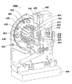
図5は本発明による改良されたイオナイザ400の斜視図である。熱い熱イオン金属製フィラメントをガスクラスターから放出される腐食性ガスから隔離するために、電子源として従来の設計の熱イオンフィラメントの代わりに希ガスプラズマ電子源を採用した。このイオナイザは、開口部、細い棒型電極、その構造などは前記図3、図4で低圧操作として記載した内容とほぼ同じである。衝撃イオン化電子源が熱金属フィラメントよりも希ガスプラズマであること、ガスクラスタージェットから放出される腐食性または反応性ガスにさらされる全ての構造材料が高純度グラファイトであることから、イオナイザによる金属汚染の発生は極めて低い。金属(典型的にはタングステン)フィラメントがプラズマ電子源の発生のためにプラズマ源内に採用されているが、それが隔離されているため、ガスクラスタージェットの放出する腐食性・反応性成分との相互作用がない。改良されたイオナイザ400はガスクラスター軸129を囲んでいる。イオナイザの上流または入力端には延長チューブ402がある。イオナイザの下流または出口には出口電極404がある。複数の開口406(3つを例示した)は、ガスクラスタージェット軸129に沿ってやってくるガスクラスターを衝撃イオン化するための希ガスプラズマ電子源からの電子をイオン化領域に導入する。A−A面またはB−B面での断面図を後に図示する。電気絶縁体の支持体408は、ガスクラスタージェット軸129に対してイオナイザを適当な位置に固定し、対象物の処理のためにGCIBを加速するエネルギーである高電圧VACCをイオナイザ本体に与えるため電気的バイアスを許容する。延長チューブ402は、長さLEを有し、イオナイザ400とスキマー開口(図13の120)との高い電圧差によってイオナイザ入口端からイオナイザ内で形成された陽イオンが逆流することを防止する作用がある。延長チューブ403はイオン化電圧(VACC)であり、上流方向における、イオナイザ400内のイオンを外部の電界から遮断する。支持プレート410については図7の所で説明する。
FIG. 5 is a perspective view of an
図6は図5で示された改良イオナイザ400の断面図450を示す。図5をB−B面でカットした斜視図である。細い棒型電極452(図では3つを指示)の部分的円筒配列が、支持プレート454と電気的に接続し支持されている。電気接続ターミナル456は、支持プレート454と細い棒型電極452をバイアスして電気的に接続されている。細い棒型電極452の部分的円筒配列は、ガスクラスタージェット軸(図5の129)を実質的に同心とする。細い棒型の電子反発電極458(図では3つを指示)の部分的円筒配列は支持プレート460により電気的に接続し支持されている。細い棒型の電子反発電極458の部分的円筒配列は、ガスクラスタージェット軸(図5の129)を実質的に同心とする。電気接続ターミナル462は、支持プレート460と細い棒型の陽極458をバイアスして電気的に接続されている。細い棒型のイオン反発電極464(図では2つを指示)の部分的円筒配列は、支持プレート466と電気的に接続し支持されている。細い棒型のイオン反発電極464の部分的円筒配列は、ガスクラスタージェット軸(図5の129)を実質的に同心とする。電気接続ターミナル468は、支持プレート466と細い棒型の陽極464をバイアスして電気的に接続されている。希ガスプラズマ電子源は、プラズマボディ470、プラズマチャンバ472、熱イオンフィラメント476、希ガス入力開口486、複数のプラズマ源チャンバ放出開口480(7つのうちの1つについて指示)を含み構成される。2つのフィラメント締め付けクランプ478(断面図では一方のみ指示)が、1−1/2回転のピッグテイル(pigtail 図7で詳述する)型タングステンフィラメントである熱イオンフィラメント476との電気的接続を与える。電子加速電極488は複数の開口482(図では7つのうちの1つについて指示)を有する。電子減速電極490は、複数の開口484(図では7つのうちの1つについて指示)を有する。複数の開口484、482、480は、複数のプラズマ源チャンバ放出開口480から開口482を通って、開口484を抜けるように、すべてが連通されている。
FIG. 6 shows a
図7は図5で示された改良イオナイザ400の断面図500を示す。図5をB−B面でカットした図である。この図はイオナイザ400が径R0のクリア開口を有することを示している。好ましい具体例では、R0は17mmである。細い陽極452(図では15のうちの3つについて指示)の部分的円筒配列の径はR1を有する。好ましい具体例では、R1は22mmである。細い棒型電子反発電極458(図では13のうちの3つについて指示)の部分的円筒配列の径はR2を有する。好ましい具体例では、R2は33mmである。細い棒型イオン反発電極464(図では11のうちの2つについて指示)の部分的円筒配列の径はR3を有する。好ましい具体例では、R3は46mmである。改良されたイオナイザ400の活性イオン化領域は径R0と、細い棒型電子反発電極458の部分的円筒配列の反対側を支持する対面支持プレート(図5の410)と支持プレート460との間の距離Lにより、規定される円筒状容積を有する。好ましい具体例ではLは約2.8R0である。Lの値は1.8R0以上が好ましい。延長チューブの長さはLEである。好ましい具体例ではLEは約4R0である。LEは2R0以上が好ましく、LEが長いと一般的に放出イオンの逆流を減少させる効果がある。
FIG. 7 shows a
図8は希ガスプラズマ電子源の放出開口の構造550を詳細に示した図である。7つの放出開口のうち、6つの開口480(図では1つのみ指示)が均等の間隔で約18mmの径の円周552上に並び、7つ目が中心開口554に配置されている。挿入図556は、開口480をさらに詳細に示している。内径が約3mmであり、出口側の径が約5mmである。対応する電子加速電極488の開口は約5.5mmであり、対応する電子減速電極490の開口は約6mmである。
FIG. 8 shows in detail the
図9は、改良イオナイザ400の電極のバイアスを詳細に示したシステム600の概略図である。熱イオンフィラメント476は、絶縁体602によってプラズマチャンバボディ470から隔離されている。希ガスがプラズマチャンバ472内に希ガス入力開口486を通じて導入される。ガス供給チューブ622は、圧縮希ガス(好ましくはアルゴン)を遠隔制御ガス弁624(好ましくは光ファイバーコントロール入力を有する質量流量制御弁)を通して供給する。ガス弁はガス供給チューブ628を通して希ガス入力開口486からプラズマチャンバ472内に低圧ガスの入力を制御する。前記遠隔制御ガス弁624は、ガス供給チューブ628内の低圧ガスを通して高電圧絶縁破壊を回避するため、イオナイザの電圧(約VACC)を有する。絶縁されたガス供給チューブ622は、ガス管を通じて高電圧放電を防止し、1気圧以上の雰囲気下でガスのみを含む。フィラメント電源608は、熱電子の放出を促進するために熱イオンフィラメント476にフィラメント電圧VFを供給する。フィラメント電源608は、3〜5Vの約140〜200Aで制御される。アーク電源610は、熱イオンフィラメント476に対応する陽性のプラズマチャンバボディ470にバイアスするようにアーク電圧を供給する。アーク電源610は、典型的には固定電圧VA約35Vであり、プラズマチャンバ内でプラズマを形成して電子を加速する手段を与える。フィラメント電流は、アーク電源610により供給されたアーク電流を調整するために制御される。アーク電源610は、プラズマアークに5Aのアーク電流を与えることができる。プラズマチャンバ472内のアークによりチャンバ内にアルゴンプラズマが生成する。アルゴンプラズマ中の電子は、プラズマチャンバ472から引き出され、加速-減速抽出システムによってイオナイザに誘導される。電子減速電極490は電子バイアス電源612によってプラズマチャンバボディ470に対応して正にバイアスされている。電子バイアス電源612は、バイアス電圧VBを与える。VBは30〜400Vの範囲で制御可能に調整される。電子加速電極488は電子抽出電源616により電子減速電極490に対応して正にバイアスされている。電子抽出電源616は電子抽出電圧VEEを与える。VEEは、20〜250Vの範囲で制御可能に調整される。加速電源620は、加速電圧VAccを供給し、細い棒型陽極452、電子減速電極490をバイアスし、延長チューブ(図5の402)、出口電極(図5の404)には、接地に対して正にバイアスする。VAccは、イオナイザ400内で生成したガスクラスターイオンのための加速電位であり、1〜80kVで制御調整される。電子反発電源614は、電子反発のバイアス電圧VERを与えて、VAccに対して電子反発電極を負にバイアスする。VERは50〜100Vで制御調整される。イオン反発電源618はイオン反発のバイアス電圧VIRを与え、イオン反発電極464をVAccに対して正にバイアスする。VIRは、50〜150Vで制御調整される。光ファイバーコントローラー630は、ケーブル634を通じて電気制御信号を受け、それらを光信号に変えて、接地された制御システムからの信号を用いた高い電位でのコンポーネントの操作を制御する光ファイバーコントロールリンク632に送信する。光ファイバーコントロールリンク632は制御信号を、制御可能なガス弁624、フィラメント電源608、アーク電源610、電子バイアス電源612、電子反発電源614、電子抽出電源616、そしてイオン反発電源618にそれぞれ送信する。
FIG. 9 is a schematic diagram of a
図10は、希ガスプラズマ電子源でプラズマを発生させ、電子を抽出するシステムの一部640の概略図である。アルゴンプラズマ642はプラズマチャンバ(図9の472)内で生成される。電子644はアルゴンプラズマ642から引き抜かれ、改良イオナイザ400の活性イオン化領域に導入される。図4で述べたように、引き抜かれた電子644は静電的に軌道に閉じ込められ、ガスクラスターをイオン化し、または細い棒型陽極452に衝突し、或いは電子減速電極490で大量の低エネルギー第二電子を生じる。第二電子は、空間電荷を中性に維持するように、正にイオン化されたガスクラスタージェットが中性になろうとする要求に応じて低エネルギー電子を与え、新しく形成されたイオン化クラスタージェットを空間電荷が中性に維持されるように保証する役割を果たす。制御可能なガス弁624はガス供給チューブ628を通じてプラズマチャンバ(図6の472)内に低圧アルゴンガスを継続して供給するので、複数の開口646を通してプラズマチャンバ(図6の472)から希ガス(好ましくはアルゴン)の継続的流れがあり、プラズマチャンバ(図6の472)内の圧力がプラズマチャンバの外側の活性領域内よりも高くなる。この流れはガスクラスタージェットから放出される反応性、腐食性ガスの侵入を低減し、プラズマチャンバ内で熱イオンフィラメント(図9の476)と反応することを防止する。もちろん、複数の開口646を通ってプラズマチャンバ内に反応性ガスが、ある程度逆流拡散するかもしれない。しかし、その量は極めて少なく実際には影響がない。少量のタングステンが熱イオンフィラメントから揮発すること、複数の開口646を通って処理に金属汚染が混入することも予測できるが、従来のGCIB処理に比較すれば極めて少量である。従って、反応性ガスと熱イオンフィラメントとの相互作用は制限され、すべての電極およびそれらを支持するプレートは高純度のグラファイトから構成されているので、改良されたイオナイザ400は、反応性ガスとイオナイザとの相互作用の結果金属汚染が生じる機会はほとんどないのである。
FIG. 10 is a schematic diagram of a
図11は第二の好ましい具体例の一部650の概略図で、プラズマチャンバボディ662内からの抽出開口656(6のうち1つを指示)、658(6のうち1つを指示)、668(6のうち1つを指示)、電子加速電極654、電子減速電極652をそれぞれ構成要素とする。この構造においては、図8の構造で採用された中心開口(図8の544)は省かれている。そして開口パターンは残された6つの抽出開口のみからなる。減速電極652の位置666には中心開口(図10と比較して)がないことに注意。中心開口を省くことにより、対応するプラズマ電子源チャンバ664から引き出される電子の量の大きな減少がなく、フィラメント476から揮発するタングステンの侵入用視界(line-of-sight)の立体角(solid angle)が著しく削減される。従って、パフォーマンスの僅かな低下だけで、イオナイザからの金属汚染のさらなる低減が実現する。
FIG. 11 is a schematic view of a
図12は第三の好ましい具体例の一部670の概略図で、プラズマチャンバボディ680内からの抽出開口676(7のうち1つを指示)、686(7のうち1つを指示)、684(7のうち1つを指示)、電子加速電極674、電子減速電極672をそれぞれ構成要素とする。希ガス入力開口682がプラズマ形成のためにプラズマチャンバ678の中に希ガスを導入する。この構造においては、抽出開口の構造に中心開口(図8の554)が図8に示されるのと同様に含まれている。プラズマチャンバボディ(図10の470)の位置が回転したような構造680であり、フィラメント476の位置が抽出開口に対してオフセットされているので、フィラメント476からの揮散タングステンが直接浸入視界に入っていない。従って、パフォーマンスの低下なしで、イオナイザからの金属汚染がさらなる低減が実現する。
FIG. 12 is a schematic view of a
図13は、本発明の改良されたイオナイザ400を組み込んだGCIB処理装置700の典型的な構造の基本要素を示す図である。電気絶縁支持体408によってガスクラスタージェット軸129の周りを取り巻きつつ、改良イオナイザ400が軸に沿って配置されている。スキマー開口120を通過した後、超音速ガスジェット118は改良イオナイザ400の延長チューブ402に導入される。改良イオナイザ400の中で、超音速ガスジェットのガスクラスターは電子衝撃イオン化法によりイオン化され、その結果得られるGCIB128は実質的には空間電荷が中性に維持される。加速電源620は1〜80kVの範囲で制御調整可能であり、加速電圧VAccを与えてGCIBを加速する。抑制電源720は抑制電圧VSを抑制電極142に与え改良イオナイザ400からガスクラスターイオンを引き出し、GCIB128に集束させ、下流の電子が逆流することおよび加速電源620への負荷を防止する。VSは0〜50kVの範囲で制御調製可能である。ガスクラスターイオンは、出口電極404と抑制電極142の間で生成される強力な電界によってイオナイザ400から引き出される。図9で詳述したように、フィラメント電源608、アーク電源610、電子バイアス電源612、電子反発電源614、電子抽出電源616、イオン反発電源618はケーブル710を通じてイオナイザ400にバイアス電圧および電流を与える。システムコントローラ702は、ケーブル712を通じてコントローラ220を、ケーブル714を通じて抑制電源720を、ケーブル716を通じて加速電源620を、ケーブル634を通じて光ファイバーコントローラ630を、それぞれ制御し調整する信号を送信する。光ファイバーコントローラ630はケーブル634によって受けた電気信号を光信号に変換し、光ファイバーコントロールリンク632を通じて制御可能なガス弁624を制御し、ファラメント電源608、アーク電源610、電子バイアス電源612、電子反発電源614、電子抽出電源616、イオン反発電源618へ光信号を送信する。ガス容器704は圧縮希ガス706、好ましくはアルゴンを収容する。圧力調節器718は希ガスの圧力を1〜2気圧の範囲に調節する。絶縁ガス供給チューブ622は、接地された圧力調節器718からイオン化電圧(約VAcc)の遠隔制御可能なガス弁624に圧力調節ガスを導入する。遠隔制御可能なガス弁624は、イオナイザ400のプラズマチャンバ472への低圧ガス流を制御する。遠隔制御可能なガス弁624からの低圧希ガスは、ガス管628を通じて、絶縁フィードスルー708を抜けてプラズマチャンバ472内へ流入する。GCIB128は、対象物152への望ましくない金属、粒子汚染を与えないで対象物152を制御可能に処理する。
FIG. 13 is a diagram illustrating the basic elements of a typical structure of a
図14は本発明のイオナイザによる半導体処理における金属汚染の減少効果を示したグラフである。グラフは、反応性エッチングガスクラスターイオンで半導体ウエハをGCIB処理したときに、表面に生じる金属汚染を、図2(左側の棒グラフ、S.N.で示す)の従来技術のイオナイザでの性能と、図3、4(中央の棒グラフ、Reflexで示す)の本発明のイオナイザや、さらに改良された本発明(右側の棒グラフ、PEGで示す)のイオナイザ400の性能を比較したものである。すべてのウエハは腐食性のガスが混合された1×10¹⁵ガスクラスターのGCIB処理を受けたものである。図2(左側棒グラフ)の自己中和型イオナイザのデータはTXRF法により測定されたもの、本発明の図3、4(中央の棒グラフ)のイオナイザと、本発明(右側棒グラフ)のイオナイザ400を用いて図8に示す構造である7つの電子抽出開口を有する方法を使用した場合のデータは、気相分解−誘導結合プラズマ質量分析法(Vapor Phase Decomposition - Inductively Coupled Plasma Mass Spectrometry (VPD ICPMS) )により測定されたものである。本発明のイオナイザ400による金属汚染の減少は著しいものがある。イオナイザ400によれば、金属の性能も、O2−NF3の場合も腐食性のガスを含まない場合と同等以上である。図14からは必ずしも明らかではないが、本発明のイオナイザ400によればタングステン汚染もかなり減少し腐食性ガスがプラズマチャンバ内で殆どフィラメントに攻撃していないことを示唆している。イオナイザ400を用いて、酸素中5%NF3を含む400時間の、アルゴン中5%GeH4を含む350時間の、各耐久性試験を行った。両方ともに、試験後も前記ガス源で普通に操作を継続できた。両方とも、テスト後に評価のために終了したところ、フィラメント上あるいはプラズマチャンバには浸食された形跡もなかった。
FIG. 14 is a graph showing the effect of reducing metal contamination in semiconductor processing by the ionizer of the present invention. The graph shows the metal contamination that occurs on the surface when a semiconductor wafer is GCIB treated with reactive etching gas cluster ions, the performance of the prior art ionizer of FIG. 2 (left bar graph, indicated by SN), FIG. 3 compares the performance of the ionizer of the present invention of FIGS. 3 and 4 (center bar graph, indicated by Reflex) and the
図5、6、7、9、10、11、12、13は、イオン化電子源供給として一つのプラズマ電子源(複数の開口は有するが)を有するが、本発明の範囲・趣旨におけるイオナイザは、イオナイザのイオン化領域に大量のイオン化電子の供給促進のために、イオン化領域に電子を供給する2以上のプラズマ電子源を有する構成にできるということは、当業者において容易に理解されるだろう。また、前記種々の具体例以外にも、本発明の趣旨の範囲内で様々な変更や他の実施例も可能であることが理解されるべきである。 5, 6, 7, 9, 10, 11, 12, and 13 have one plasma electron source (having a plurality of openings) as an ionization electron source supply, but an ionizer in the scope and spirit of the present invention is It will be readily understood by those skilled in the art that a configuration having two or more plasma electron sources for supplying electrons to the ionization region can be used to facilitate supply of a large amount of ionization electrons to the ionization region of the ionizer. In addition to the various specific examples, it should be understood that various modifications and other examples are possible within the scope of the present invention.
Claims (14)
ガスクラスタージェット軸に略平行に配置され、且つ 前記ガスクラスタージェット軸の周りの略円筒配列に部分的に配置された、略直線状の棒型電極の第一セットであって、前記円筒配列の両側の入力端と出力端との間で、前記ガスクラスタージェット軸に沿って方向付けされたガスクラスターを含むガスクラスタージェットが通過するイオン化領域を前記円筒配列内に画定する、棒型電極の第一セットと、
前記円筒配列内の前記イオン化領域から隔離して配置されている熱イオンフィラメントを有し、ガスクラスターイオンビームを形成するためにガスクラスターの少なくとも一部をイオン化する電子を、前記イオン化領域に導入するように構成された少なくとも1つのプラズマ電子源と、を備えることを特徴とするイオナイザ。An ionizer for gas cluster ion beam formation:
A first set of substantially linear rod-shaped electrodes disposed substantially parallel to a gas cluster jet axis and partially disposed in a substantially cylindrical array around the gas cluster jet axis, A first electrode of a rod-shaped electrode that defines an ionization region in the cylindrical array through which a gas cluster jet including a gas cluster directed along the gas cluster jet axis passes between an input end and an output end on both sides. One set,
Electrons that ionize at least a portion of the gas cluster are introduced into the ionization region to form a gas cluster ion beam having a thermionic filament disposed in isolation from the ionization region in the cylindrical array. And at least one plasma electron source configured as described above.
前記略直線状の棒型電極の第三セットがイオン反発電極として作動するように電気的にバイアスされた、請求項4記載のイオナイザ。The second set of substantially linear rod electrodes is electrically biased to operate as an electron repelling electrode;
The ionizer of claim 4, wherein the third set of substantially linear rod electrodes is electrically biased to operate as an ion repelling electrode.
該イオン化領域が長さLを有し、Lが1.8R0と同等以上である、請求項2記載のイオナイザ。The ionization region is defined as a generally cylindrical shape having a clear aperture of diameter R0, wherein R0 is less than R1;
The ionizer of claim 2, wherein the ionization region has a length L, and L is equal to or greater than 1.8R0.
前記入力端には、陽イオンが当該入力端を抜けて抽出されることを減少させる延長チューブを含む、請求項1記載のイオナイザ。The ionization region is defined in a generally cylindrical shape having a clear opening of diameter R0;
The ionizer of claim 1, wherein the input end includes an extension tube that reduces extraction of positive ions through the input end.
前記プラズマチャンバ内に電子を放出する加熱された前記熱イオンフィラメントと、
前記プラズマチャンバ内に希ガスを導入する開口と、
前記プラズマチャンバ内に前記希ガスプラズマを発生させるための電子を加速する手段と、
加速−減速電極と、
前記プラズマチャンバ内のプラズマから前記イオン化領域へ電子を抽出するバイアス手段と、
を含む請求項10記載のイオナイザ。The at least one plasma electron source comprises:
The heated thermionic filament that emits electrons into the plasma chamber;
An opening for introducing a rare gas into the plasma chamber;
Means for accelerating electrons for generating the noble gas plasma in the plasma chamber;
An acceleration-deceleration electrode;
Bias means for extracting electrons from the plasma in the plasma chamber to the ionization region;
The ionizer according to claim 10.
減圧雰囲気エンクロージャ(enclosure)と;
ガスクラスターイオンビームを形成するために、ガスクラスタージェット内の少なくとも一部のガスクラスターをイオン化するエンクロージャ内のイオナイザであって、
(a)ガスクラスタージェット軸に略平行に配置され、且つ 前記ガスクラスタージェット軸の周りに略円筒配列で部分的に配置された、略直線状の棒型電極の第一セットであって、前記円筒配列の両側の入力端と出力端との間で、前記ガスクラスタージェット軸に沿って方向付けされたガスクラスターを含むガスクラスタージェットが通過するイオン化領域を前記円筒配列内に画定する、棒型電極の第一セット、及び、
(b)前記円筒配列内の前記イオン化領域から隔離して配置されている熱イオンフィラメントを有し、ガスクラスターイオンビームを形成するためにガスクラスターの少なくとも一部をイオン化する電子を、前記イオン化領域に導入するように構成された少なくとも1つのプラズマ電子源、を備えるイオナイザと;
前記ガスクラスターイオンビームを加速する前記エンクロージャ内の加速手段と;
前記ガスクラスターイオンビームによって照射される前記エンクロージャ内の対象物を固定する手段と、
を含む処理装置。A gas cluster ion beam processing apparatus for processing an object by gas class cluster ion beam irradiation:
A vacuum enclosure;
An ionizer in an enclosure that ionizes at least some gas clusters in a gas cluster jet to form a gas cluster ion beam,
(A) a first set of substantially linear rod-shaped electrodes disposed substantially parallel to a gas cluster jet axis and partially disposed in a substantially cylindrical arrangement around the gas cluster jet axis, A rod shape defining an ionization region in the cylindrical array through which a gas cluster jet including a gas cluster directed along the gas cluster jet axis passes between an input end and an output end on opposite sides of the cylindrical array A first set of electrodes, and
(B) Electrons that ionize at least a portion of the gas cluster to form a gas cluster ion beam having a thermionic filament disposed separately from the ionization region in the cylindrical array. An ionizer comprising: at least one plasma electron source configured to be introduced into;
Accelerating means in the enclosure for accelerating the gas cluster ion beam;
Means for fixing an object in the enclosure irradiated by the gas cluster ion beam;
Processing equipment.
前記減圧雰囲気内に複数のガスクラスターを含むガスクラスタージェットを発生させる工程と、
ガスクラスタージェット軸を同心とする部分的な円筒配列に配置された略直線上の棒型電極のセット内のイオン化領域に、前記ガスクラスタージェット軸に沿ってガスクラスタージェットを通過させる工程と、
ガスクラスタージェット内の少なくとも一部のガスクラスターをイオン化してガスクラスターイオンビームを形成するために、前記棒型電極の円筒配列内の前記イオン化領域から隔離して配置された熱イオンフィラメントを有する少なくとも一つのプラズマ電子源から前記イオン化領域に電子を導入する工程と、
を含むガスクラスターイオンビームの形成方法。Providing a vacuum atmosphere in the enclosure;
Generating a gas cluster jet including a plurality of gas clusters in the reduced-pressure atmosphere;
Passing the gas cluster jet along the gas cluster jet axis through an ionization region in a set of substantially straight rod electrodes arranged in a partial cylindrical array concentric with the gas cluster jet axis;
Having at least a thermionic filament disposed separately from the ionization region in the cylindrical array of rod-shaped electrodes to ionize at least some gas clusters in the gas cluster jet to form a gas cluster ion beam. Introducing electrons from one plasma electron source into the ionization region;
A method for forming a gas cluster ion beam comprising:
Applications Claiming Priority (3)
| Application Number | Priority Date | Filing Date | Title |
|---|---|---|---|
| US62191304P | 2004-10-25 | 2004-10-25 | |
| US60/621,913 | 2004-10-25 | ||
| PCT/US2005/038600 WO2006047609A2 (en) | 2004-10-25 | 2005-10-25 | Ionizer and method for gas-cluster ion-beam formation |
Publications (3)
| Publication Number | Publication Date |
|---|---|
| JP2008518407A JP2008518407A (en) | 2008-05-29 |
| JP2008518407A5 JP2008518407A5 (en) | 2011-08-18 |
| JP4926067B2 true JP4926067B2 (en) | 2012-05-09 |
Family
ID=36228430
Family Applications (1)
| Application Number | Title | Priority Date | Filing Date |
|---|---|---|---|
| JP2007538189A Active JP4926067B2 (en) | 2004-10-25 | 2005-10-25 | Ionizer and method for gas cluster ion beam formation |
Country Status (4)
| Country | Link |
|---|---|
| US (1) | US7173252B2 (en) |
| EP (1) | EP1807859A2 (en) |
| JP (1) | JP4926067B2 (en) |
| WO (1) | WO2006047609A2 (en) |
Families Citing this family (73)
| Publication number | Priority date | Publication date | Assignee | Title |
|---|---|---|---|---|
| US7791047B2 (en) * | 2003-12-12 | 2010-09-07 | Semequip, Inc. | Method and apparatus for extracting ions from an ion source for use in ion implantation |
| EP1807859A2 (en) * | 2004-10-25 | 2007-07-18 | TEL Epion Inc. | Ionizer and method for gas-cluster ion-beam formation |
| JP5191650B2 (en) * | 2005-12-16 | 2013-05-08 | シャープ株式会社 | Nitride semiconductor light emitting device and method for manufacturing nitride semiconductor light emitting device |
| US7547900B2 (en) * | 2006-12-22 | 2009-06-16 | Varian Semiconductor Equipment Associates, Inc. | Techniques for providing a ribbon-shaped gas cluster ion beam |
| US7670964B2 (en) * | 2007-03-22 | 2010-03-02 | Tokyo Electron Limited | Apparatus and methods of forming a gas cluster ion beam using a low-pressure source |
| US9383138B2 (en) * | 2007-03-30 | 2016-07-05 | Tokyo Electron Limited | Methods and heat treatment apparatus for uniformly heating a substrate during a bake process |
| US7550748B2 (en) * | 2007-03-30 | 2009-06-23 | Tel Epion, Inc. | Apparatus and methods for systematic non-uniformity correction using a gas cluster ion beam |
| US7550749B2 (en) * | 2007-03-30 | 2009-06-23 | Tel Epion Inc. | Methods and processing systems for using a gas cluster ion beam to offset systematic non-uniformities in workpieces processed in a process tool |
| US20080241400A1 (en) * | 2007-03-31 | 2008-10-02 | Tokyo Electron Limited | Vacuum assist method and system for reducing intermixing of lithography layers |
| US7566888B2 (en) * | 2007-05-23 | 2009-07-28 | Tel Epion Inc. | Method and system for treating an interior surface of a workpiece using a charged particle beam |
| US9144627B2 (en) | 2007-09-14 | 2015-09-29 | Exogenesis Corporation | Methods for improving the bioactivity characteristics of a surface and objects with surfaces improved thereby |
| US7772110B2 (en) * | 2007-09-28 | 2010-08-10 | Tokyo Electron Limited | Electrical contacts for integrated circuits and methods of forming using gas cluster ion beam processing |
| US20090166555A1 (en) * | 2007-12-28 | 2009-07-02 | Olson Joseph C | RF electron source for ionizing gas clusters |
| EP2079096B1 (en) * | 2008-01-11 | 2012-04-18 | Excico Group N.V. | Ion source with filament electric discharge |
| WO2009112667A1 (en) * | 2008-01-11 | 2009-09-17 | Excico Group | Filament electrical discharge ion source |
| US20090314963A1 (en) * | 2008-06-24 | 2009-12-24 | Tel Epion Inc. | Method for forming trench isolation |
| US9103031B2 (en) * | 2008-06-24 | 2015-08-11 | Tel Epion Inc. | Method and system for growing a thin film using a gas cluster ion beam |
| US7905199B2 (en) * | 2008-06-24 | 2011-03-15 | Tel Epion Inc. | Method and system for directional growth using a gas cluster ion beam |
| US8008632B2 (en) * | 2008-07-24 | 2011-08-30 | Seagate Technology Llc | Two-zone ion beam carbon deposition |
| US7834327B2 (en) * | 2008-09-23 | 2010-11-16 | Tel Epion Inc. | Self-biasing active load circuit and related power supply for use in a charged particle beam processing system |
| US8313663B2 (en) | 2008-09-24 | 2012-11-20 | Tel Epion Inc. | Surface profile adjustment using gas cluster ion beam processing |
| US20100193898A1 (en) * | 2009-02-04 | 2010-08-05 | Tel Epion Inc. | Method for forming trench isolation using gas cluster ion beam processing |
| US8097860B2 (en) * | 2009-02-04 | 2012-01-17 | Tel Epion Inc. | Multiple nozzle gas cluster ion beam processing system and method of operating |
| US8981322B2 (en) * | 2009-02-04 | 2015-03-17 | Tel Epion Inc. | Multiple nozzle gas cluster ion beam system |
| US20100200774A1 (en) * | 2009-02-09 | 2010-08-12 | Tel Epion Inc. | Multi-sequence film deposition and growth using gas cluster ion beam processing |
| US7968422B2 (en) * | 2009-02-09 | 2011-06-28 | Tel Epion Inc. | Method for forming trench isolation using a gas cluster ion beam growth process |
| US7947582B2 (en) * | 2009-02-27 | 2011-05-24 | Tel Epion Inc. | Material infusion in a trap layer structure using gas cluster ion beam processing |
| US8226835B2 (en) * | 2009-03-06 | 2012-07-24 | Tel Epion Inc. | Ultra-thin film formation using gas cluster ion beam processing |
| FR2943173B1 (en) | 2009-03-11 | 2016-03-18 | Alcatel Lucent | IONIZATION CELL FOR MASS SPECTROMETER AND CORRESPONDING LEAK DETECTOR |
| US8877299B2 (en) * | 2009-03-31 | 2014-11-04 | Tel Epion Inc. | Method for enhancing a substrate using gas cluster ion beam processing |
| US7982196B2 (en) * | 2009-03-31 | 2011-07-19 | Tel Epion Inc. | Method for modifying a material layer using gas cluster ion beam processing |
| US8217372B2 (en) * | 2009-06-30 | 2012-07-10 | Exogenesis Corporation | Gas-cluster-jet generator and gas-cluster ion-beam apparatus utilizing an improved gas-cluster-jet generator |
| US8048788B2 (en) * | 2009-10-08 | 2011-11-01 | Tel Epion Inc. | Method for treating non-planar structures using gas cluster ion beam processing |
| US8237136B2 (en) * | 2009-10-08 | 2012-08-07 | Tel Epion Inc. | Method and system for tilting a substrate during gas cluster ion beam processing |
| US20110084214A1 (en) * | 2009-10-08 | 2011-04-14 | Tel Epion Inc. | Gas cluster ion beam processing method for preparing an isolation layer in non-planar gate structures |
| US8187971B2 (en) | 2009-11-16 | 2012-05-29 | Tel Epion Inc. | Method to alter silicide properties using GCIB treatment |
| US8992785B2 (en) * | 2010-01-15 | 2015-03-31 | Tel Epion Inc. | Method for modifying an etch rate of a material layer using energetic charged particles |
| WO2011089912A1 (en) * | 2010-01-25 | 2011-07-28 | 株式会社日立ハイテクノロジーズ | Mass spectrometry device |
| BR112012020950A2 (en) * | 2010-02-22 | 2016-04-26 | Solarion Ag | process and device for manufacturing a semiconductor layer |
| US20110240602A1 (en) * | 2010-03-30 | 2011-10-06 | Tel Epion Inc. | High-voltage gas cluster ion beam (gcib) processing system |
| US8173980B2 (en) | 2010-05-05 | 2012-05-08 | Tel Epion Inc. | Gas cluster ion beam system with cleaning apparatus |
| US8338806B2 (en) | 2010-05-05 | 2012-12-25 | Tel Epion Inc. | Gas cluster ion beam system with rapid gas switching apparatus |
| US8481340B2 (en) | 2010-06-16 | 2013-07-09 | Tel Epion Inc. | Method for preparing a light-emitting device using gas cluster ion beam processing |
| US10181402B2 (en) | 2010-08-23 | 2019-01-15 | Exogenesis Corporation | Method and apparatus for neutral beam processing based on gas cluster ion beam technology and articles produced thereby |
| US10825685B2 (en) | 2010-08-23 | 2020-11-03 | Exogenesis Corporation | Method for neutral beam processing based on gas cluster ion beam technology and articles produced thereby |
| US8847148B2 (en) * | 2010-08-23 | 2014-09-30 | Exogenesis Corporation | Method and apparatus for neutral beam processing based on gas cluster ion beam technology |
| US10670960B2 (en) * | 2010-08-23 | 2020-06-02 | Exogenesis Corporation | Enhanced high aspect ratio etch performance using accelerated neutral beams derived from gas-cluster ion beams |
| US10202684B2 (en) * | 2010-08-23 | 2019-02-12 | Exogenesis Corporation | Method for neutral beam processing based on gas cluster ion beam technology and articles produced thereby |
| US11199769B2 (en) | 2010-08-23 | 2021-12-14 | Exogenesis Corporation | Method and apparatus for neutral beam processing based on gas cluster ion beam technology |
| US20170303383A1 (en) * | 2010-08-23 | 2017-10-19 | Exogenesis Corporation | Method for neutral beam processing based on gas cluster ion beam technology and articles produced thereby |
| US9799488B2 (en) * | 2010-08-23 | 2017-10-24 | Exogenesis Corporation | Method and apparatus for neutral beam processing based on gas cluster ion beam technology |
| US9159542B2 (en) * | 2010-12-14 | 2015-10-13 | Thermo Finnigan Llc | Apparatus and method for inhibiting ionization source filament failure |
| US8440578B2 (en) | 2011-03-28 | 2013-05-14 | Tel Epion Inc. | GCIB process for reducing interfacial roughness following pre-amorphization |
| US8633452B2 (en) | 2011-07-13 | 2014-01-21 | Fei Company | Methods and structures for rapid switching between different process gases in an inductively-coupled plasma (ICP) ion source |
| US10556042B2 (en) | 2011-08-19 | 2020-02-11 | Exogenesis Corporation | Drug delivery system and method of manufacturing thereof |
| EP2758184A4 (en) | 2011-08-22 | 2015-06-24 | Exogenesis Corp | Methods for improving the bioactivity characteristics of a surface and objects with surfaces improved thereby |
| EP2747802B1 (en) | 2011-08-22 | 2022-01-12 | Exogenesis Corporation | Drug delivery system and method of manufacturing thereof |
| US8513138B2 (en) | 2011-09-01 | 2013-08-20 | Tel Epion Inc. | Gas cluster ion beam etching process for Si-containing and Ge-containing materials |
| US8512586B2 (en) | 2011-09-01 | 2013-08-20 | Tel Epion Inc. | Gas cluster ion beam etching process for achieving target etch process metrics for multiple materials |
| US8557710B2 (en) | 2011-09-01 | 2013-10-15 | Tel Epion Inc. | Gas cluster ion beam etching process for metal-containing materials |
| US8722542B2 (en) | 2012-06-08 | 2014-05-13 | Tel Epion Inc. | Gas cluster ion beam process for opening conformal layer in a high aspect ratio contact via |
| US8728947B2 (en) | 2012-06-08 | 2014-05-20 | Tel Epion Inc. | Gas cluster ion beam process for opening conformal layer in a high aspect ratio contact via |
| US8546209B1 (en) | 2012-06-15 | 2013-10-01 | International Business Machines Corporation | Replacement metal gate processing with reduced interlevel dielectric layer etch rate |
| TWI517463B (en) * | 2012-11-20 | 2016-01-11 | 佳能安內華股份有限公司 | Method for manufacturing magnetoresistance effect device |
| US20160004152A1 (en) * | 2013-02-25 | 2016-01-07 | Sean R. Kirkpatrick | Defect reduction in a substrate treatment method |
| US9209033B2 (en) | 2013-08-21 | 2015-12-08 | Tel Epion Inc. | GCIB etching method for adjusting fin height of finFET devices |
| US9105443B2 (en) | 2013-11-20 | 2015-08-11 | Tel Epion Inc. | Multi-step location specific process for substrate edge profile correction for GCIB system |
| CN105917438B (en) * | 2013-11-22 | 2018-04-24 | Tel 艾派恩有限公司 | Molecular beam strengthens GCIB processing |
| US9123505B1 (en) | 2014-02-21 | 2015-09-01 | Tel Epion Inc. | Apparatus and methods for implementing predicted systematic error correction in location specific processing |
| US9540725B2 (en) | 2014-05-14 | 2017-01-10 | Tel Epion Inc. | Method and apparatus for beam deflection in a gas cluster ion beam system |
| US9691900B2 (en) | 2014-11-24 | 2017-06-27 | International Business Machines Corporation | Dual epitaxy CMOS processing using selective nitride formation for reduced gate pitch |
| JP6545053B2 (en) * | 2015-03-30 | 2019-07-17 | 東京エレクトロン株式会社 | Processing apparatus and processing method, and gas cluster generating apparatus and generating method |
| CN106783491A (en) * | 2016-12-23 | 2017-05-31 | 信利(惠州)智能显示有限公司 | A kind of ion implantation device and its application method |
Citations (3)
| Publication number | Priority date | Publication date | Assignee | Title |
|---|---|---|---|---|
| JPH06275545A (en) * | 1993-03-22 | 1994-09-30 | Res Dev Corp Of Japan | Formation of compound thin film using gas cluster ion |
| JP2004146085A (en) * | 2002-10-22 | 2004-05-20 | Hitachi Ltd | Generation method of gas cluster ion and its generation device |
| JP2004527875A (en) * | 2000-12-26 | 2004-09-09 | エピオン コーポレイション | Charge control and dosimetry system for gas cluster ion beam |
Family Cites Families (12)
| Publication number | Priority date | Publication date | Assignee | Title |
|---|---|---|---|---|
| JP2704438B2 (en) | 1989-09-04 | 1998-01-26 | 東京エレクトロン株式会社 | Ion implanter |
| US5466929A (en) | 1992-02-21 | 1995-11-14 | Hitachi, Ltd. | Apparatus and method for suppressing electrification of sample in charged beam irradiation apparatus |
| US5814194A (en) | 1994-10-20 | 1998-09-29 | Matsushita Electric Industrial Co., Ltd | Substrate surface treatment method |
| US5959305A (en) | 1998-06-19 | 1999-09-28 | Eaton Corporation | Method and apparatus for monitoring charge neutralization operation |
| US6416820B1 (en) | 1999-11-19 | 2002-07-09 | Epion Corporation | Method for forming carbonaceous hard film |
| DE60041149D1 (en) * | 1999-12-06 | 2009-01-29 | Tel Epion Inc | DEVICE FOR SMOKING SUBSTRATES BY GAS CLUSTER ION RADIATION |
| US6629508B2 (en) | 1999-12-10 | 2003-10-07 | Epion Corporation | Ionizer for gas cluster ion beam formation |
| US6737643B2 (en) * | 2000-03-20 | 2004-05-18 | Epion Corporation | Detector and method for cluster ion beam diagnostics |
| JP2004504691A (en) | 2000-07-14 | 2004-02-12 | エピオン コーポレイション | GCIB size diagnosis and processed product processing |
| JP2006500741A (en) | 2002-09-23 | 2006-01-05 | エピオン コーポレーション | Gas cluster ion beam processing system and method |
| JP4977008B2 (en) * | 2004-03-17 | 2012-07-18 | ティーイーエル エピオン インク. | Method and apparatus for improving beam stability in high current gas cluster ion beam processing system |
| EP1807859A2 (en) * | 2004-10-25 | 2007-07-18 | TEL Epion Inc. | Ionizer and method for gas-cluster ion-beam formation |
-
2005
- 2005-10-25 EP EP05820956A patent/EP1807859A2/en not_active Withdrawn
- 2005-10-25 JP JP2007538189A patent/JP4926067B2/en active Active
- 2005-10-25 WO PCT/US2005/038600 patent/WO2006047609A2/en active Application Filing
- 2005-10-25 US US11/257,524 patent/US7173252B2/en active Active
Patent Citations (3)
| Publication number | Priority date | Publication date | Assignee | Title |
|---|---|---|---|---|
| JPH06275545A (en) * | 1993-03-22 | 1994-09-30 | Res Dev Corp Of Japan | Formation of compound thin film using gas cluster ion |
| JP2004527875A (en) * | 2000-12-26 | 2004-09-09 | エピオン コーポレイション | Charge control and dosimetry system for gas cluster ion beam |
| JP2004146085A (en) * | 2002-10-22 | 2004-05-20 | Hitachi Ltd | Generation method of gas cluster ion and its generation device |
Also Published As
| Publication number | Publication date |
|---|---|
| WO2006047609A2 (en) | 2006-05-04 |
| WO2006047609A8 (en) | 2007-06-28 |
| WO2006047609A3 (en) | 2007-03-01 |
| US7173252B2 (en) | 2007-02-06 |
| US20060097185A1 (en) | 2006-05-11 |
| JP2008518407A (en) | 2008-05-29 |
| EP1807859A2 (en) | 2007-07-18 |
Similar Documents
| Publication | Publication Date | Title |
|---|---|---|
| JP4926067B2 (en) | Ionizer and method for gas cluster ion beam formation | |
| US6768120B2 (en) | Focused electron and ion beam systems | |
| JP4977008B2 (en) | Method and apparatus for improving beam stability in high current gas cluster ion beam processing system | |
| JP4117507B2 (en) | Ion implantation apparatus, method for removing contaminants from the inner surface thereof, and removal apparatus therefor | |
| JP2648235B2 (en) | Ion gun | |
| CA2181076C (en) | Method and apparatus for in situ removal of contaminants from ion beam neutralization and implantation apparatuses | |
| TWI457967B (en) | Ion source with adjustable aperture used in creaing ion beam and related method | |
| US9564297B2 (en) | Electron beam plasma source with remote radical source | |
| US7842931B2 (en) | Extraction electrode manipulator | |
| KR102213049B1 (en) | Extraction electrode assembly voltage modulation in an ion implantation system | |
| US20110240602A1 (en) | High-voltage gas cluster ion beam (gcib) processing system | |
| EP1247434A2 (en) | Gas cluster ion beam low mass ion filter | |
| EP1738388A2 (en) | Method and apparatus for improved processing with a gas-cluster ion beam | |
| WO2009042459A1 (en) | Single wafer implanter for silicon-on-insulator wafer fabrication | |
| US6879109B2 (en) | Thin magnetron structures for plasma generation in ion implantation systems | |
| JP2015170598A (en) | Plasma-based material modification using plasma source with magnetic confinement | |
| US8993982B2 (en) | Switchable ion gun with improved gas inlet arrangement | |
| US20090166555A1 (en) | RF electron source for ionizing gas clusters | |
| US6891173B2 (en) | Ion implantation systems and methods utilizing a downstream gas source | |
| EP3518268A1 (en) | Charged-particle source and method for cleaning a charged-particle source using back-sputtering | |
| JP2837023B2 (en) | Ion implanter with improved ion source life | |
| JP2009283459A (en) | Multimode ion source | |
| JP2000235959A (en) | Doping treatment method |
Legal Events
| Date | Code | Title | Description |
|---|---|---|---|
| A621 | Written request for application examination |
Free format text: JAPANESE INTERMEDIATE CODE: A621 Effective date: 20081024 |
|
| RD12 | Notification of acceptance of power of sub attorney |
Free format text: JAPANESE INTERMEDIATE CODE: A7432 Effective date: 20081024 |
|
| A521 | Request for written amendment filed |
Free format text: JAPANESE INTERMEDIATE CODE: A821 Effective date: 20081024 |
|
| A131 | Notification of reasons for refusal |
Free format text: JAPANESE INTERMEDIATE CODE: A131 Effective date: 20110125 |
|
| A601 | Written request for extension of time |
Free format text: JAPANESE INTERMEDIATE CODE: A601 Effective date: 20110422 |
|
| A602 | Written permission of extension of time |
Free format text: JAPANESE INTERMEDIATE CODE: A602 Effective date: 20110502 |
|
| A601 | Written request for extension of time |
Free format text: JAPANESE INTERMEDIATE CODE: A601 Effective date: 20110524 |
|
| A602 | Written permission of extension of time |
Free format text: JAPANESE INTERMEDIATE CODE: A602 Effective date: 20110531 |
|
| A601 | Written request for extension of time |
Free format text: JAPANESE INTERMEDIATE CODE: A601 Effective date: 20110624 |
|
| A524 | Written submission of copy of amendment under article 19 pct |
Free format text: JAPANESE INTERMEDIATE CODE: A524 Effective date: 20110628 |
|
| A521 | Request for written amendment filed |
Free format text: JAPANESE INTERMEDIATE CODE: A523 Effective date: 20110629 |
|
| A602 | Written permission of extension of time |
Free format text: JAPANESE INTERMEDIATE CODE: A602 Effective date: 20110701 |
|
| A521 | Request for written amendment filed |
Free format text: JAPANESE INTERMEDIATE CODE: A821 Effective date: 20110628 |
|
| A131 | Notification of reasons for refusal |
Free format text: JAPANESE INTERMEDIATE CODE: A131 Effective date: 20110725 |
|
| A521 | Request for written amendment filed |
Free format text: JAPANESE INTERMEDIATE CODE: A523 Effective date: 20111024 |
|
| TRDD | Decision of grant or rejection written | ||
| A01 | Written decision to grant a patent or to grant a registration (utility model) |
Free format text: JAPANESE INTERMEDIATE CODE: A01 Effective date: 20120110 |
|
| A01 | Written decision to grant a patent or to grant a registration (utility model) |
Free format text: JAPANESE INTERMEDIATE CODE: A01 |
|
| A61 | First payment of annual fees (during grant procedure) |
Free format text: JAPANESE INTERMEDIATE CODE: A61 Effective date: 20120207 |
|
| FPAY | Renewal fee payment (event date is renewal date of database) |
Free format text: PAYMENT UNTIL: 20150217 Year of fee payment: 3 |
|
| R150 | Certificate of patent or registration of utility model |
Ref document number: 4926067 Country of ref document: JP Free format text: JAPANESE INTERMEDIATE CODE: R150 Free format text: JAPANESE INTERMEDIATE CODE: R150 |
|
| R250 | Receipt of annual fees |
Free format text: JAPANESE INTERMEDIATE CODE: R250 |
|
| R250 | Receipt of annual fees |
Free format text: JAPANESE INTERMEDIATE CODE: R250 |
|
| R250 | Receipt of annual fees |
Free format text: JAPANESE INTERMEDIATE CODE: R250 |
|
| R250 | Receipt of annual fees |
Free format text: JAPANESE INTERMEDIATE CODE: R250 |
|
| R250 | Receipt of annual fees |
Free format text: JAPANESE INTERMEDIATE CODE: R250 |
|
| R250 | Receipt of annual fees |
Free format text: JAPANESE INTERMEDIATE CODE: R250 |
|
| R250 | Receipt of annual fees |
Free format text: JAPANESE INTERMEDIATE CODE: R250 |
|
| R250 | Receipt of annual fees |
Free format text: JAPANESE INTERMEDIATE CODE: R250 |
|
| R250 | Receipt of annual fees |
Free format text: JAPANESE INTERMEDIATE CODE: R250 |