JP4920131B2 - Manufacturing method of microstructure or nanostructure on substrate - Google Patents
Manufacturing method of microstructure or nanostructure on substrate Download PDFInfo
- Publication number
- JP4920131B2 JP4920131B2 JP2000504598A JP2000504598A JP4920131B2 JP 4920131 B2 JP4920131 B2 JP 4920131B2 JP 2000504598 A JP2000504598 A JP 2000504598A JP 2000504598 A JP2000504598 A JP 2000504598A JP 4920131 B2 JP4920131 B2 JP 4920131B2
- Authority
- JP
- Japan
- Prior art keywords
- wafer
- microstructure
- nanostructure
- crystal
- lattice
- Prior art date
- Legal status (The legal status is an assumption and is not a legal conclusion. Google has not performed a legal analysis and makes no representation as to the accuracy of the status listed.)
- Expired - Lifetime
Links
Images


Classifications
-
- B—PERFORMING OPERATIONS; TRANSPORTING
- B82—NANOTECHNOLOGY
- B82Y—SPECIFIC USES OR APPLICATIONS OF NANOSTRUCTURES; MEASUREMENT OR ANALYSIS OF NANOSTRUCTURES; MANUFACTURE OR TREATMENT OF NANOSTRUCTURES
- B82Y30/00—Nanotechnology for materials or surface science, e.g. nanocomposites
-
- H—ELECTRICITY
- H01—ELECTRIC ELEMENTS
- H01L—SEMICONDUCTOR DEVICES NOT COVERED BY CLASS H10
- H01L21/00—Processes or apparatus adapted for the manufacture or treatment of semiconductor or solid state devices or of parts thereof
- H01L21/02—Manufacture or treatment of semiconductor devices or of parts thereof
- H01L21/04—Manufacture or treatment of semiconductor devices or of parts thereof the devices having at least one potential-jump barrier or surface barrier, e.g. PN junction, depletion layer or carrier concentration layer
- H01L21/18—Manufacture or treatment of semiconductor devices or of parts thereof the devices having at least one potential-jump barrier or surface barrier, e.g. PN junction, depletion layer or carrier concentration layer the devices having semiconductor bodies comprising elements of Group IV of the Periodic System or AIIIBV compounds with or without impurities, e.g. doping materials
- H01L21/30—Treatment of semiconductor bodies using processes or apparatus not provided for in groups H01L21/20 - H01L21/26
- H01L21/302—Treatment of semiconductor bodies using processes or apparatus not provided for in groups H01L21/20 - H01L21/26 to change their surface-physical characteristics or shape, e.g. etching, polishing, cutting
- H01L21/306—Chemical or electrical treatment, e.g. electrolytic etching
-
- B—PERFORMING OPERATIONS; TRANSPORTING
- B82—NANOTECHNOLOGY
- B82Y—SPECIFIC USES OR APPLICATIONS OF NANOSTRUCTURES; MEASUREMENT OR ANALYSIS OF NANOSTRUCTURES; MANUFACTURE OR TREATMENT OF NANOSTRUCTURES
- B82Y10/00—Nanotechnology for information processing, storage or transmission, e.g. quantum computing or single electron logic
-
- H—ELECTRICITY
- H01—ELECTRIC ELEMENTS
- H01L—SEMICONDUCTOR DEVICES NOT COVERED BY CLASS H10
- H01L21/00—Processes or apparatus adapted for the manufacture or treatment of semiconductor or solid state devices or of parts thereof
- H01L21/02—Manufacture or treatment of semiconductor devices or of parts thereof
- H01L21/02002—Preparing wafers
-
- H—ELECTRICITY
- H01—ELECTRIC ELEMENTS
- H01L—SEMICONDUCTOR DEVICES NOT COVERED BY CLASS H10
- H01L21/00—Processes or apparatus adapted for the manufacture or treatment of semiconductor or solid state devices or of parts thereof
- H01L21/02—Manufacture or treatment of semiconductor devices or of parts thereof
- H01L21/04—Manufacture or treatment of semiconductor devices or of parts thereof the devices having at least one potential-jump barrier or surface barrier, e.g. PN junction, depletion layer or carrier concentration layer
- H01L21/18—Manufacture or treatment of semiconductor devices or of parts thereof the devices having at least one potential-jump barrier or surface barrier, e.g. PN junction, depletion layer or carrier concentration layer the devices having semiconductor bodies comprising elements of Group IV of the Periodic System or AIIIBV compounds with or without impurities, e.g. doping materials
- H01L21/185—Joining of semiconductor bodies for junction formation
Description
【0001】
【発明の属する技術分野】
本発明は、基板上のマイクロ構造あるいはナノ構造の製造に関するものである。
【0002】
【従来の技術及び発明が解決しようとする課題】
より小さいサイズに縮小しマイクロ構造及びナノ構造は、基板の表面上に形成された微小ボリュームの格子の形をしている。微小ボリュームによって、例えば、好ましくは1ミクロンより小さいサイズの平行六面体形状のボリュームを意味している。
【0003】
一般には、半導体材料、特にシリコン、AsGa、III-V化合物、及びSiCで形成されたマイクロ構造に関心が集まっている。しかしながら、金属のような導体、及びSiO2のような誘電体材料にも関心が集まっている。
【0004】
これらのマイクロ構造あるいはナノ構造は、電子素子、光学素子、あるいは光電子素子を対象にしたものである。特に、これらの構造を用いて、量子ドット、あるいは単電子素子と呼ばれる電子素子、あるいは、クーロン閉塞電子素子、あるいは発光素子のネットワークを製造することも可能である。
【0005】
マイクロ構造を製造することを望むならば、技術は、今日マイクロ電子工学の領域における従来型のものを用いることが可能である。特に、乾式エッチングあるいは湿式エッチングを併せたリソグラフィ、イオン注入、蒸着、あるいは熱処理の原理を用いる。例えば、単結晶シリコンから成る平行六面体形状の複数のマイクロボリューム(microvolumes)(各ボリュームが側面長さ1μmで厚さ0.2μmを有し、ボリュームは0.5μmの距離で離間している)スクウェアネットワーク(square network)を形成することが望むならば、0.2μmの膜厚の単結晶シリコン層を有するSOI(Silicon-on-Insulator)を有することが可能である。感光性樹脂層がウェーハシリコン層に適用され、その感光性樹脂層は、マイクロボリューム間の間隔を表す0.5μm幅の行及び列のマトリックスを用いてその樹脂をパターン化するために電子ビームパターン発生器を用いて分離される。露出部を現像するため、樹脂現像は行列マトリックスに対応するシリコン層を被覆しない。次に、ウェーハに、樹脂に関係するシリコンの選択的除去のためのプラズマエッチングを施す。にエッチング操作は、下位のシリコン層に達したら完了である。樹脂を除去した後、1μm×1μm×0.2μmのサイズでかつ0.5μm間隔を有するマイクロボリュームのネットワークが得られる。必要なら、マイクロボリューム間のスペースを、熱酸化処理あるいはCVD型の蒸着処理のいずれかを用いて、SiO2のような誘電体層で充填する。
【0006】
マイクロボリュームのネットワークも、以下の論文によって開示されてようなリソグラフィによって形成してもよい:その論文は、S.H.ZAIDIらによる“Scalable Fabrication and Optical Characterization of nm Si Structures”(Mat.Res.Soc.Symp.Proc.Vol.358, 957-968頁,Material Research Society)である。
【0007】
これらの技術を用いると、1μmのオーダーあるいは10分の数μmのオーダーのサイズのマイクロ構造を形成することが可能である。リソグラフィにおいて最高の分解能を得るために、電子ビームパターン発生器、あるいは248nmあるいは193nmの波長で使用するフォトリピーター(Photo Repeater)を使用する。
【0008】
経済的に許容される方法でかつ大きな表面上において、所定の配列プランでマイクロ構造を得ることを所望ならば、非常に小さいサイズ(例えば、10分の数nm)のマイクロボリュームを使ってマイクロ構造を形成する方法は知られていない。
【0009】
しかしながら、例えば、前記マトリックスにおける最初の材料の原子を挿入するイオン注入を用いて、第二の材料から成るマトリックス内に第一の材料から成るマイクロボリュームを形成すること(ここで、それらの原子がマトリックス内に集まって凝結するような濃度とし、かつ熱処理を行う)が可能であることに注目するべきである。この方法においては、10nmオーダーのSiO2マトリックスにおいて凝結したシリコンを得ることは可能である。前記技術は、例えば、T.KOMADAらによる“Control of and Mechanizm for Room Temperature Visible Light Emission from Silicon Nanostructure in SiO2, formed by Si+ Ion Implantation”(Mat.Res.Soc.Symp.Proc.Vol.358, 163-168頁,1995,Material Research Society)に記載されている。しかしながら、得られた凝結物はマトリックスにランダムに分散している。
【0010】
同様に、表面上で堆積を行うことによって(例えば、蒸発によって)、表面上にランダムに分散した凝縮の核を得ることは可能である。PING LI及びK.SATTLERによる論文“Generation and Structural Analysis of Silicon Nanoparticles”(Mat.Res.Soc.Symp.Proc.Vol.358, 123-126頁,1995,Material Research Society)では、シリコンあるいはグラファイト表面上へのシリコンの蒸着について開示している。
【0011】
これらのマイクロ構造の応用は多数あり、各構造の特定の特性に依存する。これらの特性は、これらの材料におけるキャリアーの電子状態におけるサイズ効果、表面及び界面効果、及び粒界層の存在あるいは不在に関わるものである。特別な応用は、特に、光発生しない固体結晶状態でのシリコンのような材料からの光エミッターの製造である。別な応用は、マイクロボリュームの構造における電子導体の量子閉じ込め、あるいはクーロン閉塞効果を基礎にした電子素子の製造である。この応用については、D.W.Boeringer及びによる論文“Modelling the Multiplicity of Conductance Structures in Clusters of Silicon Quantum Dots”(Mat.Res.Soc.Symp.Proc.Vol.358, 569-574頁,1995,Material Research Society)に記載されている。
【0012】
【課題を解決するための手段】
本発明は、経済的な方法でかつ大きな表面上に、現在製造可能なマイクロボリュームよりはるかに小さいサイズ、例えば10分の数nmのマイクロボリュームを収容することができるマイクロ構造を製造することを可能にするために設計したものである。さらに、これらのマイクロ構造は、ランダムに分散するのではなく、所定のプランに従って配置する。
【0013】
本発明は、半導体、導体、あるいは誘電体のいずれかの結晶材料に適用可能なマイクロ構造あるいはナノ構造を形成する方法を提唱する。
【0014】
従って、本発明の主な内容は、基板上のマイクロ構造あるいはナノ構造の製造方法であって、
−結晶材料から成る第一のウェーハ(1)の一方の表面(3)を結晶材料から成る第二のウェーハ(2)の一方の表面(4)に接触して配置することによって結合する段階であって、その配置は、前記表面に存在する結晶格子が、前記の2つのウェーハの界面の一方の側を拡張する、結晶ゾーン(8)内の結晶欠陥格子及び/又は歪み格子の形成を可能にするように少なくとも一つの不整合パラメーターを提供するように、かつ、少なくとも一つの前記格子がマイクロ構造あるいはナノ構造を画定するようにする段階と、
−前記の2つのウェーハのうちの一方を薄板化して、他方のウェーハによって形成された基板(10)上の格子欠陥及び/又は格子歪みを露出する段階と、
を備えていることを特徴とするマイクロ構造あるいはナノ構造の製造方法を提供することである。
【0015】
不整合パラメーターは、前記表面の結晶格子における回転シフトの所定の角度から決めてもよい。得られる欠陥の格子、いわゆる“ねじれ(twist)”格子は、らせん転位の格子である。
【0016】
不整合パラメーターは、接触されたウェーハの表面の結晶材料の間の結晶単位胞パラメーターにおける差から決めてもよい。得られる格子変形は“ミスフィット(misfit)”である。
【0017】
不整合パラメーターは、少なくともウェーハのひとつの面が、この面に対応する方向の通常の結晶面に関連してシフトしている、所定の角度から決めてもよい。通常の結晶面に関連する、方向が決められない結晶面(一つだけあるいは両方)は、微傾斜と呼ばれる。このとき、格子変形は“ミスカット”と呼ばれる。
【0018】
不整合パラメーターの全組み合わせは、例えば、シフトした回転を有する2つの異なる材料を結合することによって可能になる。それから、複数の格子が形成される。
【0019】
接触は疎水性タイプのもの、すなわち、前記ウェーハの表面に直接結合することによるものであることが好ましい。しかし、親水性タイプのもの、すなわち、例えば、一方のウェーハの片面上、あるいは両ウェーハの面上に形成された酸化層のような中間層を含むものでもよい。
【0020】
方法も、接触が格子欠陥及び/又は格子歪みの形成に対して不十分ならば、その形成を完全にするためか、言い換えると、その形成を完了するための熱処理段階を少なくとも一つ含んでいるが好都合である。また、この処理は接触ウェーハの表面の原子間結合の強化を促進するものである。この熱処理は、薄板化段階の前、あるいはその後に実施する。
【0021】
薄板化段階は、研削、機械的研磨あるいは化学的研磨の方法から選択することによって実施してもよい。
【0022】
薄板化段階は、続く熱処理段階の間の劈開平面を生成することが可能なマイクロキャビティを作るために、接触段階の前に、接触表面を介して所望の薄板化に対応する所定の深さにイオン注入を行う段階を実施する必要があるウェーハの一方を劈開することによって行われる。薄板化段階がこのように実施されるならば、少なくとも一つの熱処理段階は、格子欠陥及び/又は格子歪みの形成を同時に完成あるいは完了すること、接触ウェーハの表面間の原子間結合を強化すること、及び劈開面を生成することを可能にするように設計されている。
【0023】
薄板化段階の後のマイクロ構造あるいはナノ構造の使用に依存して、段階は、結晶ゾーンに関連した格子欠陥及び/又は格子歪みの選択的な処理を含むように設計されている。これは、特に、前記結晶ゾーンに関係した前記結晶欠陥の物理的/電子的あるいは光電子的振る舞いにおける差を強調すること、あるいはもっと一般的に、結晶ゾーン内あるいは結晶ゾーン上のマイクロボリュームあるいはナノボリュームの境界を定めることにつながる。この選択処理段階は、前記結晶ゾーンが互いに電気的に接続する結晶コンタクトパッドを形成するように、格子欠陥及び/又は格子歪みを導電性にすることをふくんでいてもよい。この場合には、結晶欠陥での拡散が好ましいリンの拡散が生ずるだろう。また、選択処理段階は電気的絶縁化を含んでおり、そのため、前記結晶ゾーンは電気的に絶縁されている結晶パッドを形成する。この場合には、格子欠陥及び/又は格子歪みへ攻撃(これにより、電気的絶縁体の堆積につながる)のために、化学研磨を用いてもよい。化学研磨は、金属不純物あるいはドープしている不純物堆積することに起因した格子欠陥及び/又は格子歪みの修飾相の形成の前に行ってもよい。
【0024】
上記方法により形成される格子欠陥は、2つのウェーハの結合面のいずれかのサイドに薄く広がる。他方、これらの欠陥に誘起される歪みは、転位周期のオーダーの距離を超えた、ウェーハ内での界面のいずれかの面を広げる。従って、ウェーハの一方の薄板化は、同じオーダーである界面からの距離で処理を停止してもよい。このように露出された表面では、結晶欠陥に達する前に、表面歪みの領域は均一ではなく、かつ内部の格子欠陥を反映している。選択処理段階は、例えば、薄板化段階によって露出した結晶材料との結晶単位胞の不整合を有する材料のエピタキシーによる堆積を含んでもよく、このとき、この蒸着された結晶材料は、格子欠陥の基礎格子に対応した整列した一連のアイランド(island)を形成する。
【0025】
選択処理の電気的絶縁は、電気伝導がトンネル効果あるいはファウラー−ノルドハイム効果のような物理的効果によって生ずることが可能なタイプのものである。
【0026】
選択処理の段階はまた、結晶ゾーンが、半導体ゾーンによって互いに接続された、あるいはポテンシャル障壁を有する結晶パッドを形成するような格子欠陥及び/又は歪みを処理することを含んでいてもよい。
【0027】
本発明の他の目的は、上記の方法に従い、その接触領域が半導体材料から成るウェーハを用いて得られたことを特徴とする、基板上のマイクロ構造あるいはナノ構造を提供することである。接触する表面の少なくとも一方の面は、SiC、又は、AsGaあるいはGaAlAsのようなIII-V半導体材料から成るものであってもよい。
【0028】
本発明の他の目的は、マイクロ構造あるいはナノ構造は上記の方法を用いて形成する方法であって、一方のウェーハはシリコンから成り、かつ薄板化されたウェーハであり、その方法は、マイクロ構造あるいはナノ構造を絶縁層上にマイクロボリュームのシリコンによって形成するを可能にするものである。
【0029】
【発明の実施の形態】
本発明は、添付図面を用いて非限定的例として与えられる以下の記載を読むことによって、本発明はさらによく理解され、他の利点及び特徴も明らかになるだろう。
【0030】
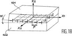
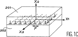
図1(A)、図1(B)及び図1(C)は、本発明の方法の3つの実施形態を示している。X1,X2及びX3は結晶軸を示している。図1(A)で示した場合には、欠陥密度(あるいは欠陥間の平均距離)を制御するパラメーターは、ウェーハ1とウェーハ2との接触面に表した結晶ネットワーク間に存在する回転角βである。図1(B)で示した場合には、欠陥密度(あるいは欠陥間の平均距離)を制御するパラメーターは、ウェーハ101とウェーハ102との接触した結晶面間に存在する回転角αである。図1(C)で示した場合には、欠陥密度(あるいは欠陥間の平均距離)を制御するパラメーターは、ウェーハ201とウェーハ202との接触した2つの結晶材料間の単位胞の不整合f1である。
【0031】
以下の表は、(シリコン100についての)界面欠陥格子の周期pに対する、回転角βの値、傾斜角(angle of orientation)αの値、および、単位胞の不整合f1の値を示したものである。
【表1】

例によると、図1(A)で示した方法の実施形態に対して、回転角βで結合したシリコン(100)の2つのウェーハは、その界面上に、19.2の周期を有するらせん転位の矩形格子を形成する。ウェーハをp/2=9.6nmにまで薄板化した後で、かつ上記の技術の一つを用いて現像した後、9.6nmより小さいサイズを有する2.7×1015/m2のナノ構造の密度を得る。
【0033】
図1(B)で示した方法の実施形態で19.2nmの周期を得るために、一方のウェーハは、は、<100>方向に0.8°のシフトを有する微傾斜面を有し、かつ、シリコンウェーハの非微傾斜面に結合したものを準備する。このとき、得られたナノ構造密度2.7×10¹⁵/m2である。
【0034】
図1(C)で示した方法の実施形態に対しては、シリコン(100)ウェーハは、表面上にSiGeの層を有する第二のウェーハに結合している。不整合f1は2.1%であり、19.2nmの周期を有するコーナー転位の界面格子が形成される。SiGeを有するウェーハを約10nmまで薄板化した後には、前述のものと同じオーダーのナノ構造密度を得る。ゲルマニウムウェーハの結合は、2倍の不整合、従って4倍のナノ構造密度を生成する。
【0035】
(100)以外の面を使用してもよい。例えば、(111)面は界面に六角形あるいは三角形の転位格子を生成する。(110)面は長方形格子を生成する。異なる方向を有し、互いに結合した2つの面も、周期的あるいはほぼ周期的な格子を生成する。
【0036】
図1(A)で示した方法の実施形態を以下に詳細に説明する。説明を簡単にするために、結晶欠陥格子は、それが通常格子歪みに関連し、かつ選択処理もその格子歪みにおいて行われ得るという条件で検討される。
【0037】
図1(A)は、(100)結晶面を有し、かつそれぞれ符号3及び4の対面する平面を有する、2つのシリコンウェーハ1及び2を接触する段階を示している。平面3及び4は、それらを疎水性にするように表面処理をしている。これが、表面3と表面4との密接な付着を保証する。前記表面処理は、例えば、親水性の酸による研磨段階で完了する化学洗浄段階を含んでいる。より詳細は、文献、“Handbook of Semiconductor Wafer Cleaning Technology”(Werner KERN監修、Noyes Publication,Park Ridge, New York)の中の一つの章である、Gregg S, HIGASHI及びYves J.CHABALによる“Silicon Surface Chemical Composition and Morphology”(433頁など)を参考にするべきである。
【0038】
面3及び4の接触は、2つの表面に現れた結晶格子が、所定の角度β、例えば0.6°だけ互いに回転してずれていることを保証するように、例えば、室温で分子結合によって行われる。
【0039】
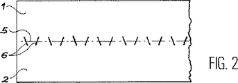
これら結合されたウェーハによって形成されたユニットは、約30分間950℃程度の温度で熱処理を実施しなければならない。この熱処理の間、2つのウェーハの間により強力な原子間結合が形成される。2つの結晶格子の間に形成された捻れ角が与えられると、結晶欠陥の格子、例えば、転位の格子が2つのウェーハ間の界面に近接して、その界面の中央部に狭い厚さの層(10分の数nmあるいは100分の数nm)内に形成される。これは図2に示しており、符号5がこの界面を表し、結晶欠陥(あるいは転位)は符号6で示している。
【0040】
これらの転位が、約40nmの階段を有する規則的な2次元格子(図では四角形)を形成する例を示している。これらの事実は、H.Foll及びD.ASTによる、文献“TEM observations on Grain Boundaries in Sintered Silicon”(Philosophical Magazine A, 1979, vol.40, N°5, 589-610頁)において、理論的に説明されている。この文献の596頁には、このタイプの転位の格子の写真が掲載されている。
【0041】
2つの隣接する転位間の間隔は、両方のウェーハの結晶格子間の回転角βに依存する。この間隔の値は、sin(β/2)に対して逆に変化する。β=5°に対しては、隣接転位間の間隔は4.4nmと得られている。
【0042】
図2で示したユニットからマイクロ構造を得るために、必要なことは(研削、機械的研磨、あるいは化学的研磨によって)2つのウェーハの一方を研磨して、転位ゾーンに届くときに研磨操作を停止することだけである。これは、マイクロ構造を符号3で示した図3に示した。マイクロ構造は、ウェーハ2の最大の部分で形成された基板10上に配置している
【0043】
さらに特別なやり方で、結晶ゾーン8を囲繞する結晶欠陥を区別するために、表面処理を行ってもよい。
【0044】
例えば、隣接する結晶ゾーン8を除去することなく、化学浴によって、結晶欠陥6を選択的に除去することが可能である。ここで示した実施形態においては、SECCO(登録商標)あるいはWRIGHT(登録商標)の化学浴を用いることができる。この場合には、シリコンマイクロボリュームの格子は、スペースによって互いに絶縁される40nmの格子ステップサイズを有する矩形形状で形成されている。
【0045】
マイクロボリューム9の面方向誘電体絶縁を作ってもよい。この目的にために、例えば、マイクロ構造を酸化する、あるいはCVD蒸着を行うことは可能である。複数の応用に対して、マイクロ構造を堆積した酸化層は、マイクロボリューム9間の絶縁堆積層11だけを維持するために、図4で示したように、高さを下げてもよい。この場合には、絶縁材料の格子を転位の格子の代わりに用いることによって得られる。
【0046】
表面処理はまた、導電性、あるいは絶縁性、あるいは本発明に関連して半導体の転位の格子を与えるために行うものである。この方法では、マイクロボリュームあるいは結晶パッドは、導電性結合によって互いに電気的に接続され、又は、半導体ゾーンによって電気的に絶縁されあるい電気的に接続されるかのいずれかであり、また、ポテンシャル障壁を有する。電気的絶縁の観点からは、これも、絶縁部の一部を介して電気伝導がトンネル効果あるいはファウラー−ノルドハイム効果あるいは他の物理的効果によって生じるように、絶縁膜を含んでいる。転位の格子を導電性にするために、転位部で好適に拡散するリンの拡散を行ってもよい。
【0047】
薄くする段階を行う別の可能な方法は、仏国特許第2,681,4721号公開公報に記載されているような、処理中のウェーハの劈開を行うような方法を行うことを含んでいる。この目的のためには、例えば、接触する表面の所定の深さでマイクロキャビティを得るように、このウェーハに陽子を注入することである。この表面を清浄化処理及び結合処理を行う。それから熱処理を行う。これによって、マイクロキャビティ層によって、転位が発生し、それと同時に劈開が可能になる。
【0048】
一方のウェーハ(基板を形成することになる方)は、SOIと呼ばれるSOIウェーハ(Silicon-On-Insulator)であってもよく、また、他方のウェーハは固体シリコン基板であってもよい。本発明の方法は、絶縁膜上にシリコンのマイクロボリュームの格子を供給する。
【0049】
結晶材料から成る2つのウェーハは、例えば、シリコンウェーハとガリウムウェーハ、あるいは、シリコンウェーハとゲルマニウムウェーハのように、異なるタイプであってもよい。さらに、ウェーハは均一であることは必要とされない。接触することになる表面は、単純には結晶材料から成り、ウェーハの残りは他の構造を提供することも可能である。
【0050】
上記のように、マイクロ構造あるいはナノ構造も、歪みの格子から得てもよい。この歪み格子は、様々な方法によって形成してもよい。
【0051】
歪み格子は、結晶単位胞の不整合を有する結晶材料の薄板化したウェーハ上に、エピタキシー法(MOCVD, MBE, 液晶層エピタキシー)を用いて堆積することによって、形成してもよい。島状成長モードを用いて、圧縮(引張り(順不同))が必要となるゾーンによって得られた好適な核形成サイトが博板化したウェーハより小さい(大きい(順不同))メッシュ(mesh)を形成するのを促進する。このように、下の格子に対応するサイズである、整列した一群の島を形成する。
【0052】
この堆積は、図1(C)で示した本発明の実施形態を用いて実施できる。ユニットは、上記のように、(100)方向を有するシリコンウェーハとSiGe層を有するウェーハとを用いて、この実施形態に対応して準備した。薄板化の後、符号202がシリコンウェーハを示し、かつ符号201’がSiGe層の残留部を示している図5に示したユニットを得る;純粋ゲルマニウムの堆積は、ストランスキー−クラスタノフ型の成長条件の下で行った。ゲルマニウムのナノアイランド210が、張力の下での歪みゾーンにおける転位格子の節(node)の真下で核形成する。
【図面の簡単な説明】
【図1】 (A)本発明の製造方法の第一の実施形態によって、2つのウェーハの結晶材料を接触する段階を示すための概略斜視図である。(B)本発明の製造方法の第二の実施形態によって、2つのウェーハの結晶材料を接触する段階を示すための概略斜視図である。(C)本発明の製造方法の第三の実施形態によって、2つのウェーハの結晶材料を接触する段階を示すための概略斜視図である。
【図2】 図1における2つのウェーハを接触させた後にその2つのウェーハで形成されたユニットの概略側面図である。
【図3】 本発明の方法の薄板化段階の後の図2で示したユニットの概略側面図である。
【図4】 本発明を用いて得られたマイクロ構造のユニットの概略側断面図である。
【図5】 本発明を用いて得られた他のマイクロ構造のユニットの概略側断面図である。
【符号の説明】
1、2、101、102、201,202 ウェーハ
3、4 平坦な表面
5 界面
6 結晶欠陥
7 マイクロ構造
8 結晶ゾーン
9 マイクロボリューム
10 基板
11 絶縁堆積層
201’残留部
210 ゲルマニウムのナノアイランド[0001]
BACKGROUND OF THE INVENTION
The present invention relates to the fabrication of microstructures or nanostructures on a substrate.
[0002]
[Prior art and problems to be solved by the invention]
Shrinking to smaller sizes, microstructures and nanostructures are in the form of a microvolume lattice formed on the surface of the substrate. By microvolume is meant, for example, a parallelepiped-shaped volume, preferably of a size smaller than 1 micron.
[0003]
In general, there is an interest in microstructures formed of semiconductor materials, particularly silicon, AsGa, III-V compounds, and SiC. However, conductors, and also interested in the dielectric material such as SiO 2 are gathered, such as metal.
[0004]
These microstructures or nanostructures are intended for electronic elements, optical elements, or optoelectronic elements. In particular, using these structures, it is also possible to manufacture an electronic device called a quantum dot or a single electronic device, a coulomb blocking electronic device, or a network of light emitting devices.
[0005]
If it is desired to produce a microstructure, the technology can use conventional ones in the field of microelectronics today. In particular, the principle of lithography, ion implantation, vapor deposition, or heat treatment combined with dry etching or wet etching is used. For example, a plurality of parallelepiped microvolumes made of single crystal silicon (each volume has a side length of 1 μm and a thickness of 0.2 μm, and the volumes are separated by a distance of 0.5 μm) If it is desired to form a square network, it is possible to have an SOI (Silicon-on-Insulator) having a single crystal silicon layer with a thickness of 0.2 μm. A photosensitive resin layer is applied to the wafer silicon layer, and the photosensitive resin layer is an electron beam pattern for patterning the resin using a 0.5 μm wide row and column matrix representing the spacing between microvolumes. Separated using a generator. In order to develop the exposed portion, the resin development does not cover the silicon layer corresponding to the matrix matrix. Next, the wafer is subjected to plasma etching for selective removal of silicon related to the resin. The etching operation is complete when the lower silicon layer is reached. After removing the resin, a microvolume network with a size of 1 μm × 1 μm × 0.2 μm and a 0.5 μm spacing is obtained. If necessary, the space between the microvolumes is filled with a dielectric layer such as SiO 2 using either a thermal oxidation process or a CVD type deposition process.
[0006]
A network of microvolumes may also be formed by lithography as disclosed by the following paper: the paper “Scalable Fabrication and Optical Characterization of nm Si Structures” (Mat. Res. Soc. Symp. Proc. Vol. 358, 957-968, Material Research Society).
[0007]
Using these techniques, it is possible to form a microstructure with a size on the order of 1 μm or a few tenths of μm. In order to obtain the highest resolution in lithography, an electron beam pattern generator or a photo repeater used at a wavelength of 248 nm or 193 nm is used.
[0008]
If it is desired to obtain a microstructure with a given array plan in an economically acceptable manner and on a large surface, the microstructure can be used using a microvolume of very small size (eg, a few tenths of nm) The method of forming is not known.
[0009]
However, for example, using ion implantation to insert atoms of the first material in the matrix, a microvolume made of the first material is formed in the matrix made of the second material (where the atoms are It should be noted that it is possible to achieve a concentration such that it collects and condenses in the matrix and is heat treated. In this method, it is possible to obtain silicon condensed in a SiO 2 matrix of the order of 10 nm. The technique is described in, for example, “Control of and Mechanizm for Room Temperature Visible Light Emission from Silicon Nanostructure in SiO 2 , formed by Si + Ion Implantation” (Mat. Res. Soc. Symp. Proc. Vol. 358). 163-168, 1995, Material Research Society). However, the resulting agglomerates are randomly dispersed in the matrix.
[0010]
Similarly, by performing deposition on the surface (eg, by evaporation), it is possible to obtain condensed nuclei randomly dispersed on the surface. In the article “Generation and Structural Analysis of Silicon Nanoparticles” by PING LI and K. SATTLER (Mat. Res. Soc. Symp. Proc. Vol. 358, 123-126, 1995, Material Research Society) Discloses the deposition of silicon.
[0011]
There are many applications for these microstructures, depending on the specific characteristics of each structure. These properties are related to the size effect in the electronic state of the carriers in these materials, the surface and interface effects, and the presence or absence of grain boundary layers. A particular application is in particular the production of light emitters from materials such as silicon in the solid crystalline state where no light is generated. Another application is the manufacture of electronic devices based on the quantum confinement of electron conductors in the structure of microvolumes or the Coulomb blockage effect. For this application, see the article “Modeling the Multiplicity of Conductance Structures in Clusters of Silicon Quantum Dots” (Dat. Res. Soc. Symp. Proc. Vol. 358, 569-574, 1995, Material Research Society) by DWBoeringer and others. Are listed.
[0012]
[Means for Solving the Problems]
The present invention makes it possible to produce microstructures that can accommodate microvolumes that are much smaller in size, for example, a few tenths of a nanovolume, on a large surface, on a large surface. It is designed to make it. Furthermore, these microstructures are not randomly distributed but arranged according to a predetermined plan.
[0013]
The present invention proposes a method for forming a microstructure or a nanostructure applicable to any crystalline material of a semiconductor, conductor, or dielectric.
[0014]
Therefore, the main content of the present invention is a method of manufacturing a microstructure or nanostructure on a substrate,
In the joining step by placing one surface (3) of the first wafer (1) of crystalline material in contact with one surface (4) of the second wafer (2) of crystalline material The arrangement allows the formation of crystal defect lattices and / or strain lattices in the crystal zone (8) where the crystal lattice present on the surface extends on one side of the interface of the two wafers. Providing at least one mismatch parameter such that at least one of the lattices defines a microstructure or a nanostructure; and
-Thinning one of the two wafers to expose lattice defects and / or lattice distortions on the substrate (10) formed by the other wafer;
It is providing the manufacturing method of the micro structure or nano structure characterized by comprising.
[0015]
The mismatch parameter may be determined from a predetermined angle of rotational shift in the surface crystal lattice. The resulting defect lattice, the so-called “twist” lattice, is a lattice of screw dislocations.
[0016]
The mismatch parameter may be determined from the difference in crystal unit cell parameters between crystalline materials on the surface of the contacted wafer. The resulting lattice deformation is a “misfit”.
[0017]
The misalignment parameter may be determined from a predetermined angle at which at least one surface of the wafer is shifted relative to a normal crystal plane in a direction corresponding to this surface. Crystal planes (one or both) that are not oriented in relation to the normal crystal plane are called fine tilts. At this time, the lattice deformation is called “miscut”.
[0018]
All combinations of mismatch parameters are possible, for example, by combining two different materials with shifted rotation. A plurality of grids are then formed.
[0019]
The contact is preferably of the hydrophobic type, i.e. by bonding directly to the surface of the wafer. However, it may be of a hydrophilic type, that is, an intermediate layer such as an oxide layer formed on one side of one wafer or on both sides.
[0020]
The method also includes at least one heat treatment step to complete the formation if contact is insufficient for the formation of lattice defects and / or lattice strains, in other words to complete the formation. Is convenient. This treatment also promotes strengthening of interatomic bonds on the surface of the contact wafer. This heat treatment is performed before or after the thinning step.
[0021]
The thinning step may be performed by selecting from grinding, mechanical polishing or chemical polishing methods.
[0022]
The thinning step is performed at a predetermined depth corresponding to the desired thinning through the contact surface prior to the contact step to create a microcavity capable of generating a cleavage plane during the subsequent heat treatment step. This is done by cleaving one of the wafers where the ion implantation step needs to be performed. If the thinning step is carried out in this way, at least one heat treatment step can complete or complete the formation of lattice defects and / or lattice strains simultaneously, strengthen interatomic bonds between the contact wafer surfaces. And designed to allow the generation of cleaved surfaces.
[0023]
Depending on the use of microstructures or nanostructures after the thinning step, the step is designed to include selective treatment of lattice defects and / or lattice strains associated with the crystal zone. This particularly emphasizes differences in the physical / electronic or optoelectronic behavior of the crystal defects associated with the crystal zone, or more generally, microvolumes or nanovolumes within or on the crystal zone. Leading to demarcation. This selective processing step may include making lattice defects and / or lattice strains conductive so that the crystal zones form crystal contact pads that are electrically connected to each other. In this case, diffusion of phosphorus with crystal defects is preferred, which will result in diffusion of phosphorus. Also, the selective processing step includes electrical insulation, so that the crystal zone forms an electrically isolated crystal pad. In this case, chemical polishing may be used to attack lattice defects and / or lattice distortions, thereby leading to electrical insulator deposition. Chemical polishing may be performed prior to the formation of a lattice defect and / or a lattice distortion modified phase resulting from the deposition of metal impurities or doped impurities.
[0024]
The lattice defects formed by the above method spread thinly on either side of the bonding surface of the two wafers. On the other hand, the strain induced in these defects widens any surface of the interface within the wafer beyond a distance on the order of the dislocation period. Therefore, the thinning of one of the wafers may stop at a distance from the interface that is the same order. On the exposed surface in this manner, the area of surface distortion is not uniform and reflects internal lattice defects before reaching the crystal defects. The selective processing step may include, for example, the deposition by epitaxy of a material having a crystal unit cell mismatch with the crystalline material exposed by the thinning step, where the deposited crystalline material is the basis for lattice defects. Form an aligned series of islands corresponding to the grid.
[0025]
The electrical isolation of the selective process is of the type in which electrical conduction can be caused by physical effects such as tunneling effects or Fowler-Nordheim effects.
[0026]
The stage of selective processing may also include processing lattice defects and / or strains such that the crystal zones form crystal pads connected to each other by a semiconductor zone or having a potential barrier.
[0027]
Another object of the present invention is to provide a microstructure or nanostructure on a substrate, characterized in that, according to the above method, the contact area is obtained using a wafer made of a semiconductor material. At least one surface of the contacting surface may be made of SiC or a III-V semiconductor material such as AsGa or GaAlAs.
[0028]
Another object of the present invention is a method of forming a microstructure or nanostructure using the above method, wherein one wafer is made of silicon and is a thinned wafer. Alternatively, nanostructures can be formed on the insulating layer with microvolumes of silicon.
[0029]
DETAILED DESCRIPTION OF THE INVENTION
The invention will be better understood and other advantages and features will become apparent upon reading the following description, given by way of non-limiting example using the accompanying drawings, in which:
[0030]
1A, 1B and 1C show three embodiments of the method of the present invention. X 1 , X 2 and X 3 represent crystal axes. In the case shown in FIG. 1A, the parameter for controlling the defect density (or the average distance between the defects) is the rotation angle β existing between the crystal networks represented on the contact surface between the wafer 1 and the wafer 2. is there. In the case shown in FIG. 1B, the parameter for controlling the defect density (or the average distance between the defects) is the rotation angle α existing between the crystal planes where the
[0031]
The table below shows the values of the rotation angle β, the angle of orientation α, and the unit cell mismatch f1 for the period p of the interface defect lattice (for silicon 100). It is.
[Table 1]
By way of example, for the embodiment of the method shown in FIG. 1A, two wafers of silicon (100) bonded at a rotation angle β have a screw dislocation rectangle with a period of 19.2 on their interface. A lattice is formed. After thinning the wafer to p / 2 = 9.6 nm and developing using one of the above techniques, the density of nanostructures of 2.7 × 10 15 / m 2 with a size less than 9.6 nm is achieved. obtain.
[0033]
To obtain a period of 19.2 nm in the method embodiment shown in FIG. 1B, one wafer has a slightly inclined surface with a 0.8 ° shift in the <100> direction and silicon Prepare a wafer bonded to the non-slightly inclined surface of the wafer. At this time, the obtained nanostructure density is 2.7 × 10 15 / m 2 .
[0034]
For the method embodiment shown in FIG. 1C, a silicon (100) wafer is bonded to a second wafer having a layer of SiGe on the surface. The mismatch f1 is 2.1%, and a corner dislocation interface lattice having a period of 19.2 nm is formed. After thinning the SiGe-containing wafer to about 10 nm, a nanostructure density of the same order as described above is obtained. Bonding germanium wafers produces a double mismatch, and thus a fourfold nanostructure density.
[0035]
Surfaces other than (100) may be used. For example, the (111) plane generates a hexagonal or triangular dislocation lattice at the interface. The (110) plane generates a rectangular grid. Two faces with different orientations and joined together also produce a periodic or nearly periodic grating.
[0036]
An embodiment of the method shown in FIG. 1A will be described in detail below. For simplicity of explanation, the crystal defect lattice is considered under the condition that it is usually associated with lattice strain and that the selection process can also be performed at that lattice strain.
[0037]
FIG. 1A shows the step of contacting two silicon wafers 1 and 2 having a (100) crystal plane and having facing planes 3 and 4 respectively. Planes 3 and 4 are surface treated to make them hydrophobic. This ensures a close adhesion between the surface 3 and the surface 4. The surface treatment includes, for example, a chemical cleaning step completed in a polishing step with a hydrophilic acid. For more details, see “Silicon Surface” by Gregg S, HIGASHI and Yves J. CHABAL, a chapter in the literature, “Handbook of Semiconductor Wafer Cleaning Technology” (supervised by Werner KERN, Noyes Publication, Park Ridge, New York). “Chemical Composition and Morphology” (page 433, etc.) should be consulted.
[0038]
Contact between faces 3 and 4 is made, for example, by molecular bonding at room temperature to ensure that the crystal lattices appearing on the two surfaces are offset from each other by a predetermined angle β, eg 0.6 °. .
[0039]
The unit formed by these bonded wafers must be heat treated at a temperature on the order of 950 ° C. for about 30 minutes. During this heat treatment, a stronger interatomic bond is formed between the two wafers. Given a twist angle formed between two crystal lattices, a crystal defect lattice, for example, a dislocation lattice is in close proximity to the interface between the two wafers and a thin layer at the center of the interface. (A few tenths of a nm or a few hundredths of a nm). This is shown in FIG. 2, where
[0040]
In the example, these dislocations form a regular two-dimensional lattice (rectangle in the figure) having a step of about 40 nm. These facts are theoretically described in the literature “TEM observations on Grain Boundaries in Sintered Silicon” by H. Foll and D. AST (Philosophical Magazine A, 1979, vol. 40, N ° 5, 589-610). Explained. Page 596 of this document contains a photograph of a lattice of this type of dislocation.
[0041]
The spacing between two adjacent dislocations depends on the rotation angle β between the crystal lattices of both wafers. The value of this interval changes inversely with respect to sin (β / 2). For β = 5 °, the spacing between adjacent dislocations is 4.4 nm.
[0042]
To obtain the microstructure from the unit shown in FIG. 2, all that is required is to polish one of the two wafers (by grinding, mechanical polishing, or chemical polishing) and perform the polishing operation when it reaches the dislocation zone. It only stops. This is shown in FIG. The microstructure is arranged on a
In a more special way, a surface treatment may be performed to distinguish crystal defects surrounding the crystal zone 8.
[0044]
For example, the crystal defect 6 can be selectively removed by a chemical bath without removing the adjacent crystal zone 8. In the embodiment shown here, a SECCO® or WRIGHT® chemical bath can be used. In this case, the silicon microvolume lattice is formed in a rectangular shape having a lattice step size of 40 nm that is insulated from each other by a space.
[0045]
A planar dielectric insulation of the microvolume 9 may be made. For this purpose, it is possible, for example, to oxidize the microstructure or to perform CVD deposition. For multiple applications, the oxide layer deposited with the microstructure may be lowered in height as shown in FIG. 4 to maintain only the insulating
[0046]
The surface treatment is also performed to provide a dislocation lattice of semiconductors in connection with the present invention. In this method, the microvolumes or crystal pads are either electrically connected to each other by conductive bonds, or are electrically isolated or electrically connected by a semiconductor zone, and the potential Has a barrier. From the point of view of electrical isolation, this also includes an insulating film so that electrical conduction occurs through a portion of the insulating portion due to the tunnel effect, Fowler-Nordheim effect, or other physical effects. In order to make the lattice of dislocations conductive, diffusion of phosphorus that preferably diffuses at the dislocations may be performed.
[0047]
Another possible method of performing the thinning step includes performing a method of cleaving the wafer being processed, as described in French Patent 2,681,4721. For this purpose, for example, protons are injected into the wafer so as to obtain microcavities at a predetermined depth of the contacting surface. The surface is cleaned and bonded. Then heat treatment is performed. Thereby, the microcavity layer causes dislocations and at the same time allows cleavage.
[0048]
One wafer (the one that will form the substrate) may be an SOI wafer (Silicon-On-Insulator) called SOI, and the other wafer may be a solid silicon substrate. The method of the present invention provides a silicon microvolume lattice on an insulating film.
[0049]
The two wafers made of crystalline material may be of different types, for example, a silicon wafer and a gallium wafer, or a silicon wafer and a germanium wafer. Furthermore, the wafer is not required to be uniform. The surface to be contacted is simply made of crystalline material, and the rest of the wafer can provide other structures.
[0050]
As mentioned above, microstructures or nanostructures may also be obtained from strained lattices. This strain grating may be formed by various methods.
[0051]
The strained lattice may be formed by depositing on a thinned wafer of crystalline material having crystal unit cell mismatch using an epitaxy method (MOCVD, MBE, liquid crystal layer epitaxy). Using island growth mode, the preferred nucleation sites obtained by zones that require compression (tensile (in no particular order)) form a smaller (large (in no particular order)) mesh (mesh) than the flaked wafer To promote In this way, an aligned group of islands is formed that is sized corresponding to the underlying grid.
[0052]
This deposition can be performed using the embodiment of the present invention shown in FIG. As described above, a unit was prepared corresponding to this embodiment using a silicon wafer having a (100) direction and a wafer having a SiGe layer. After thinning, the unit shown in FIG. 5 is obtained, in which 202 represents the silicon wafer and 201 ′ represents the remaining part of the SiGe layer; the deposition of pure germanium is a Transky-Clusternov type growth Performed under conditions. Germanium nano-
[Brief description of the drawings]
FIG. 1A is a schematic perspective view illustrating a step of contacting crystal materials of two wafers according to a first embodiment of a manufacturing method of the present invention. (B) It is a schematic perspective view for showing the step which contacts the crystal material of two wafers by 2nd embodiment of the manufacturing method of this invention. (C) It is a schematic perspective view for showing the step which contacts the crystal material of two wafers by 3rd embodiment of the manufacturing method of this invention.
2 is a schematic side view of a unit formed with two wafers after contacting the two wafers in FIG. 1; FIG.
FIG. 3 is a schematic side view of the unit shown in FIG. 2 after the thinning stage of the method of the present invention.
FIG. 4 is a schematic cross-sectional side view of a microstructure unit obtained using the present invention.
FIG. 5 is a schematic cross-sectional side view of another microstructured unit obtained using the present invention.
[Explanation of symbols]
1, 2, 101, 102, 201, 202 Wafer 3, 4
Claims (14)
−結晶材料から成る第一のウェーハ(1)の一方の表面(3)を結晶材料から成る第二のウェーハ(2)の一方の表面(4)に接触して配置することによって前記第一のウェーハを前記第二のウェーハに結合する段階であって、前記第一のウェーハの結晶材料、前記第二のウェーハの結晶材料、及び、前記表面を配置することが、前記表面に存在する結晶格子が、前記結合された2つのウェーハによって形成されるユニットの結晶層であって前記結合された2つのウェーハの間の界面に配置される結晶層内に結晶欠陥格子及び/又は歪み格子の形成を可能にするように少なくとも一つの不整合パラメーターを提供するように、かつ、少なくとも一つの前記格子がマイクロ構造あるいはナノ構造を形成するようにする段階と、
−前記の2つのウェーハのうちの一方を薄板化して、他方のウェーハによって形成された基板(10)上の結晶欠陥格子及び/又は歪み格子を露出する段階と、
−前記結晶欠陥格子及び/又は歪み格子を表面処理する段階であって、前記表面処理が、前記結晶層に対して結晶欠陥格子及び/又は歪み格子の物理的/電子的又は光電子的振る舞いにおける差を強調するものである段階と、
を備えていることを特徴とするマイクロ構造あるいはナノ構造の製造方法。A method for producing a microstructure or nanostructure on a substrate,
By placing one surface (3) of the first wafer (1) made of crystalline material in contact with one surface (4) of the second wafer (2) made of crystalline material; A step of bonding a wafer to the second wafer, wherein arranging the crystal material of the first wafer, the crystal material of the second wafer, and the surface comprises a crystal lattice present on the surface Forming a crystal defect lattice and / or strain lattice in a crystal layer of a unit formed by the two bonded wafers and disposed at an interface between the two bonded wafers. Providing at least one mismatch parameter as possible and allowing at least one said lattice to form a microstructure or nanostructure;
-Thinning one of the two wafers to expose a crystal defect lattice and / or strain lattice on the substrate (10) formed by the other wafer;
- a step of treating the surface of the crystal defects rated child及 beauty / or distortion grating, the surface treatment, physical / electronic or optoelectronic behavior of crystal defects lattice and / or distortion grating with respect to the crystal layer A stage that emphasizes the difference in
A method for producing a microstructure or a nanostructure, comprising:
Applications Claiming Priority (3)
| Application Number | Priority Date | Filing Date | Title |
|---|---|---|---|
| FR97/09264 | 1997-07-22 | ||
| FR9709264A FR2766620B1 (en) | 1997-07-22 | 1997-07-22 | PRODUCTION OF MICROSTRUCTURES OR NANOSTRUCTURES ON A SUPPORT |
| PCT/FR1998/001585 WO1999005711A1 (en) | 1997-07-22 | 1998-07-20 | Producing microstructures or nanostructures on a support |
Publications (3)
| Publication Number | Publication Date |
|---|---|
| JP2001511599A JP2001511599A (en) | 2001-08-14 |
| JP2001511599A5 JP2001511599A5 (en) | 2011-01-20 |
| JP4920131B2 true JP4920131B2 (en) | 2012-04-18 |
Family
ID=9509456
Family Applications (1)
| Application Number | Title | Priority Date | Filing Date |
|---|---|---|---|
| JP2000504598A Expired - Lifetime JP4920131B2 (en) | 1997-07-22 | 1998-07-20 | Manufacturing method of microstructure or nanostructure on substrate |
Country Status (6)
| Country | Link |
|---|---|
| US (1) | US6261928B1 (en) |
| EP (1) | EP1008169B1 (en) |
| JP (1) | JP4920131B2 (en) |
| DE (1) | DE69840480D1 (en) |
| FR (1) | FR2766620B1 (en) |
| WO (1) | WO1999005711A1 (en) |
Families Citing this family (28)
| Publication number | Priority date | Publication date | Assignee | Title |
|---|---|---|---|---|
| DE19853023A1 (en) | 1998-11-18 | 2000-05-31 | Forschungszentrum Juelich Gmbh | Process for the production of nanostructures in thin films |
| WO2001042540A1 (en) * | 1999-12-09 | 2001-06-14 | Cornell Research Foundation, Inc. | Fabrication of periodic surface structures with nanometer-scale spacings |
| FR2815121B1 (en) * | 2000-10-06 | 2002-12-13 | Commissariat Energie Atomique | PROCESS FOR REVELATION OF CRYSTALLINE DEFECTS AND / OR STRESS FIELDS AT THE MOLECULAR ADHESION INTERFACE OF TWO SOLID MATERIALS |
| FR2815026B1 (en) * | 2000-10-06 | 2004-04-09 | Commissariat Energie Atomique | METHOD FOR SELF-ORGANIZING MICROSTRUCTURES OR NANOSTRUCTURES AND MICROSTRUCTURE OR NANOSTRUCTURE DEVICE |
| FR2819099B1 (en) * | 2000-12-28 | 2003-09-26 | Commissariat Energie Atomique | METHOD FOR PRODUCING A STACKED STRUCTURE |
| US6913697B2 (en) | 2001-02-14 | 2005-07-05 | Science & Technology Corporation @ Unm | Nanostructured separation and analysis devices for biological membranes |
| US6699770B2 (en) * | 2001-03-01 | 2004-03-02 | John Tarje Torvik | Method of making a hybride substrate having a thin silicon carbide membrane layer |
| JP2002265831A (en) * | 2001-03-13 | 2002-09-18 | Ricoh Co Ltd | Ink composition and recording technology using the same |
| US6956268B2 (en) | 2001-05-18 | 2005-10-18 | Reveo, Inc. | MEMS and method of manufacturing MEMS |
| US7045878B2 (en) | 2001-05-18 | 2006-05-16 | Reveo, Inc. | Selectively bonded thin film layer and substrate layer for processing of useful devices |
| KR100425092B1 (en) * | 2001-05-29 | 2004-03-30 | 엘지전자 주식회사 | method for fabricating silicon compliant substrate |
| CN1164488C (en) * | 2001-07-25 | 2004-09-01 | 中山大学 | Process for preparing nm-class silicon carbide material |
| US7163826B2 (en) | 2001-09-12 | 2007-01-16 | Reveo, Inc | Method of fabricating multi layer devices on buried oxide layer substrates |
| US6875671B2 (en) | 2001-09-12 | 2005-04-05 | Reveo, Inc. | Method of fabricating vertical integrated circuits |
| EP1448908B1 (en) * | 2001-11-23 | 2006-02-01 | Universität Duisburg-Essen | Implant |
| JP2005279843A (en) * | 2004-03-29 | 2005-10-13 | Univ Of Tokyo | Crystal material including fine wires, method of producing it, and nanowire device using it |
| FR2876498B1 (en) * | 2004-10-12 | 2008-03-14 | Commissariat Energie Atomique | METHOD FOR PRODUCING PLANAR TRANSPARENT RESINANT HETEROSTRUCTURES |
| FR2877662B1 (en) | 2004-11-09 | 2007-03-02 | Commissariat Energie Atomique | PARTICLE NETWORK AND METHOD FOR MAKING SUCH A NETWORK |
| FR2895419B1 (en) * | 2005-12-27 | 2008-02-22 | Commissariat Energie Atomique | PROCESS FOR SIMPLIFIED REALIZATION OF AN EPITAXIC STRUCTURE |
| FR2895391B1 (en) | 2005-12-27 | 2008-01-25 | Commissariat Energie Atomique | PROCESS FOR PRODUCING ORDINATED NANOSTRUCTURES |
| FR2895571B1 (en) * | 2005-12-28 | 2008-04-18 | Commissariat Energie Atomique | METHOD FOR PRODUCING AN ELECTROLUMINESCENT PN JUNCTION IN SEMICONDUCTOR MATERIAL BY MOLECULAR BONDING |
| FR2896493B1 (en) * | 2006-01-23 | 2008-02-22 | Commissariat Energie Atomique | METHOD FOR PRODUCING A SUPPORT FOR THE GROWTH OF LOCALIZED LONG NANOSTRUCTURES |
| FR2903810B1 (en) * | 2006-07-13 | 2008-10-10 | Commissariat Energie Atomique | METHOD FOR NANOSTRUCTURING THE SURFACE OF A SUBSTRATE |
| JP2008060355A (en) * | 2006-08-31 | 2008-03-13 | Sumco Corp | Laminated wafer, and manufacturing method therefor |
| FR2925748B1 (en) | 2007-12-21 | 2010-01-29 | Commissariat Energie Atomique | DATA STORAGE MEDIUM AND ASSOCIATED METHOD |
| FR2937797B1 (en) * | 2008-10-28 | 2010-12-24 | S O I Tec Silicon On Insulator Tech | METHOD FOR MANUFACTURING AND PROCESSING A SEMICONDUCTOR-INSULATING TYPE STRUCTURE FOR DISPLACING DISLOCATIONS AND CORRESPONDING STRUCTURE |
| FR2978600B1 (en) | 2011-07-25 | 2014-02-07 | Soitec Silicon On Insulator | METHOD AND DEVICE FOR MANUFACTURING LAYER OF SEMICONDUCTOR MATERIAL |
| JP6355540B2 (en) * | 2014-12-04 | 2018-07-11 | 株式会社ディスコ | Wafer generation method |
Family Cites Families (18)
| Publication number | Priority date | Publication date | Assignee | Title |
|---|---|---|---|---|
| FR2681472B1 (en) * | 1991-09-18 | 1993-10-29 | Commissariat Energie Atomique | PROCESS FOR PRODUCING THIN FILMS OF SEMICONDUCTOR MATERIAL. |
| DE4133820A1 (en) * | 1991-10-12 | 1993-04-15 | Bosch Gmbh Robert | METHOD FOR PRODUCING SEMICONDUCTOR ELEMENTS |
| JP3237888B2 (en) * | 1992-01-31 | 2001-12-10 | キヤノン株式会社 | Semiconductor substrate and method of manufacturing the same |
| JP3192000B2 (en) * | 1992-08-25 | 2001-07-23 | キヤノン株式会社 | Semiconductor substrate and manufacturing method thereof |
| JP2908150B2 (en) * | 1992-11-27 | 1999-06-21 | 日本電気株式会社 | SOI substrate structure and manufacturing method thereof |
| FR2714524B1 (en) | 1993-12-23 | 1996-01-26 | Commissariat Energie Atomique | PROCESS FOR MAKING A RELIEF STRUCTURE ON A SUPPORT IN SEMICONDUCTOR MATERIAL |
| FR2715502B1 (en) | 1994-01-26 | 1996-04-05 | Commissariat Energie Atomique | Structure having cavities and method for producing such a structure. |
| FR2715501B1 (en) | 1994-01-26 | 1996-04-05 | Commissariat Energie Atomique | Method for depositing semiconductor wafers on a support. |
| JPH07263721A (en) * | 1994-03-25 | 1995-10-13 | Nippondenso Co Ltd | Semiconductor device and manufacture thereof |
| FR2725074B1 (en) * | 1994-09-22 | 1996-12-20 | Commissariat Energie Atomique | METHOD FOR MANUFACTURING A STRUCTURE COMPRISING A THIN SEMI-CONDUCTIVE LAYER ON A SUBSTRATE |
| US5932048A (en) * | 1995-04-06 | 1999-08-03 | Komatsu Electronic Metals Co., Ltd. | Method of fabricating direct-bonded semiconductor wafers |
| JP3441277B2 (en) * | 1995-12-26 | 2003-08-25 | 株式会社東芝 | Semiconductor device and manufacturing method thereof |
| FR2756973B1 (en) | 1996-12-09 | 1999-01-08 | Commissariat Energie Atomique | METHOD FOR INTRODUCING A GASEOUS PHASE IN A CLOSED CAVITY |
| US6155909A (en) * | 1997-05-12 | 2000-12-05 | Silicon Genesis Corporation | Controlled cleavage system using pressurized fluid |
| US5877070A (en) * | 1997-05-31 | 1999-03-02 | Max-Planck Society | Method for the transfer of thin layers of monocrystalline material to a desirable substrate |
| US5882987A (en) * | 1997-08-26 | 1999-03-16 | International Business Machines Corporation | Smart-cut process for the production of thin semiconductor material films |
| US5981400A (en) * | 1997-09-18 | 1999-11-09 | Cornell Research Foundation, Inc. | Compliant universal substrate for epitaxial growth |
| US5897362A (en) * | 1998-04-17 | 1999-04-27 | Lucent Technologies Inc. | Bonding silicon wafers |
-
1997
- 1997-07-22 FR FR9709264A patent/FR2766620B1/en not_active Expired - Fee Related
-
1998
- 1998-07-20 EP EP98939717A patent/EP1008169B1/en not_active Expired - Lifetime
- 1998-07-20 JP JP2000504598A patent/JP4920131B2/en not_active Expired - Lifetime
- 1998-07-20 WO PCT/FR1998/001585 patent/WO1999005711A1/en active Application Filing
- 1998-07-20 DE DE69840480T patent/DE69840480D1/en not_active Expired - Lifetime
- 1998-07-20 US US09/463,226 patent/US6261928B1/en not_active Expired - Lifetime
Also Published As
| Publication number | Publication date |
|---|---|
| JP2001511599A (en) | 2001-08-14 |
| EP1008169B1 (en) | 2009-01-14 |
| FR2766620A1 (en) | 1999-01-29 |
| WO1999005711A1 (en) | 1999-02-04 |
| DE69840480D1 (en) | 2009-03-05 |
| FR2766620B1 (en) | 2000-12-01 |
| EP1008169A1 (en) | 2000-06-14 |
| US6261928B1 (en) | 2001-07-17 |
Similar Documents
| Publication | Publication Date | Title |
|---|---|---|
| JP4920131B2 (en) | Manufacturing method of microstructure or nanostructure on substrate | |
| US6569748B1 (en) | Substrate and production method thereof | |
| JP4954853B2 (en) | Crystal defect and / or stress field manifestation process at the molecular adhesion interface of two solid materials | |
| EP2629320B1 (en) | Mask structure and method for defect-free heteroepitaxial deposition | |
| JP4730877B2 (en) | Method for producing relaxed silicon-germanium on an insulator via layer dislocations with reduced stress | |
| JP2001523049A (en) | Quantum ridges and quantum peaks | |
| JPH0621336A (en) | Silicon layer provided with maximized surface area and its manufacture | |
| JPH04318918A (en) | Part that consists of semiconductors | |
| EP1908097A2 (en) | Method for controlling dislocation positions in silicon germanium buffer layers | |
| JP2006522469A5 (en) | ||
| JP2018509002A (en) | Thermally stable charge trapping layer for use in the manufacture of semiconductor-on-insulator structures | |
| KR20080098424A (en) | Method for producing partial soi structures comprising zones connecting a superficial layer and a substrate | |
| JPH03165577A (en) | Semiconductor device and its manufacture | |
| US20010041419A1 (en) | Method for fabrication semiconductor device having trench isolation structure | |
| US7060587B2 (en) | Method for forming macropores in a layer and products obtained thereof | |
| JP3954095B2 (en) | Microelectronic device and manufacturing method thereof | |
| JP2023527123A (en) | SAG nanowire growth by ion implantation | |
| US20150179583A1 (en) | Semiconductor devices comprising edge doped graphene and methods of making the same | |
| JP3748726B2 (en) | Quantum wire manufacturing method | |
| JP2760345B2 (en) | Single electronic device | |
| TWI588886B (en) | Method of fabricating a semiconductor device | |
| US6074936A (en) | Method of fabricating a quantum device | |
| JPH09135017A (en) | Fabrication of quantum device | |
| JPH08236748A (en) | Quantum semiconductor device and its manufacture | |
| JP3789179B2 (en) | Quantization functional element, quantization functional device using the same, and manufacturing method thereof |
Legal Events
| Date | Code | Title | Description |
|---|---|---|---|
| A621 | Written request for application examination |
Free format text: JAPANESE INTERMEDIATE CODE: A621 Effective date: 20050707 |
|
| A131 | Notification of reasons for refusal |
Free format text: JAPANESE INTERMEDIATE CODE: A131 Effective date: 20090623 |
|
| A601 | Written request for extension of time |
Free format text: JAPANESE INTERMEDIATE CODE: A601 Effective date: 20090924 |
|
| A602 | Written permission of extension of time |
Free format text: JAPANESE INTERMEDIATE CODE: A602 Effective date: 20091001 |
|
| A521 | Request for written amendment filed |
Free format text: JAPANESE INTERMEDIATE CODE: A523 Effective date: 20091224 |
|
| A131 | Notification of reasons for refusal |
Free format text: JAPANESE INTERMEDIATE CODE: A131 Effective date: 20100525 |
|
| A601 | Written request for extension of time |
Free format text: JAPANESE INTERMEDIATE CODE: A601 Effective date: 20100825 |
|
| A602 | Written permission of extension of time |
Free format text: JAPANESE INTERMEDIATE CODE: A602 Effective date: 20100901 |
|
| A524 | Written submission of copy of amendment under article 19 pct |
Free format text: JAPANESE INTERMEDIATE CODE: A524 Effective date: 20101125 |
|
| A131 | Notification of reasons for refusal |
Free format text: JAPANESE INTERMEDIATE CODE: A131 Effective date: 20110802 |
|
| A601 | Written request for extension of time |
Free format text: JAPANESE INTERMEDIATE CODE: A601 Effective date: 20111101 |
|
| A602 | Written permission of extension of time |
Free format text: JAPANESE INTERMEDIATE CODE: A602 Effective date: 20111109 |
|
| A521 | Request for written amendment filed |
Free format text: JAPANESE INTERMEDIATE CODE: A523 Effective date: 20111201 |
|
| TRDD | Decision of grant or rejection written | ||
| A01 | Written decision to grant a patent or to grant a registration (utility model) |
Free format text: JAPANESE INTERMEDIATE CODE: A01 Effective date: 20120104 |
|
| A01 | Written decision to grant a patent or to grant a registration (utility model) |
Free format text: JAPANESE INTERMEDIATE CODE: A01 |
|
| A61 | First payment of annual fees (during grant procedure) |
Free format text: JAPANESE INTERMEDIATE CODE: A61 Effective date: 20120201 |
|
| R150 | Certificate of patent or registration of utility model |
Free format text: JAPANESE INTERMEDIATE CODE: R150 |
|
| FPAY | Renewal fee payment (event date is renewal date of database) |
Free format text: PAYMENT UNTIL: 20150210 Year of fee payment: 3 |
|
| R250 | Receipt of annual fees |
Free format text: JAPANESE INTERMEDIATE CODE: R250 |
|
| R250 | Receipt of annual fees |
Free format text: JAPANESE INTERMEDIATE CODE: R250 |
|
| R250 | Receipt of annual fees |
Free format text: JAPANESE INTERMEDIATE CODE: R250 |
|
| R250 | Receipt of annual fees |
Free format text: JAPANESE INTERMEDIATE CODE: R250 |
|
| EXPY | Cancellation because of completion of term |