JP4915059B2 - Electromagnetic wave suppressing material and electronic device - Google Patents
Electromagnetic wave suppressing material and electronic device Download PDFInfo
- Publication number
- JP4915059B2 JP4915059B2 JP2005208425A JP2005208425A JP4915059B2 JP 4915059 B2 JP4915059 B2 JP 4915059B2 JP 2005208425 A JP2005208425 A JP 2005208425A JP 2005208425 A JP2005208425 A JP 2005208425A JP 4915059 B2 JP4915059 B2 JP 4915059B2
- Authority
- JP
- Japan
- Prior art keywords
- electromagnetic wave
- ionic liquid
- wave suppressing
- suppressing material
- electronic device
- Prior art date
- Legal status (The legal status is an assumption and is not a legal conclusion. Google has not performed a legal analysis and makes no representation as to the accuracy of the status listed.)
- Expired - Fee Related
Links
Images


Description
本発明は、電子機器から発生する不要輻射対策等に用いる電磁波抑制材、及びこの電磁波抑制材を具備する電子機器に関する。 The present invention relates to an electromagnetic wave suppressing material used for measures against unnecessary radiation generated from an electronic device, and an electronic device including the electromagnetic wave suppressing material.
近年に見られる高周波数の電磁波利用の増加に伴い、電磁波ノイズによる機器の誤作動や、脳及び人体への悪影響等といった被害並びに障害が新たな環境問題として提起されている。 With the increase in the use of high-frequency electromagnetic waves seen in recent years, damages and obstacles such as malfunction of equipment due to electromagnetic noise and adverse effects on the brain and human body have been raised as new environmental problems.
例えば、免許不要であって無線通信で利用可能な周波数帯の1つである2.45GHz帯に注目してみると、これは無線LAN(IEEE802.11b)、Bluetooth、ISM(Industrial, Scientific and Medical)機器等に数多く利用されている、更には、情報機器のクロック周波数の高速化及びデジタル化に伴い、この帯域における高調波の発生も考えられる。 For example, looking at the 2.45 GHz band, which is one of the frequency bands that do not require a license and can be used for wireless communication, this is a wireless LAN (IEEE802.11b), Bluetooth, ISM (Industrial, Scientific and Medical). ) It is widely used in equipment, etc. Furthermore, with the increase in the clock frequency and digitization of information equipment, the generation of harmonics in this band is also conceivable.
このように、潜在的な電磁波発生源及び干渉被害側の双方の数と多様性とが指数関数的に増加するため、干渉の起こるリスクが天文学的に増加している。 In this way, the number and diversity of both potential electromagnetic wave sources and interference victims increase exponentially, increasing the risk of interference.
このような電磁干渉(EMI: Electromagnetic Interference)の問題に対処するためには、個々の機器が、他の機器の正常な作動を妨害するような不要な電磁波を放射させることなく(エミッションの抑制)、かつ外部から侵入する電磁波に対して何ら影響を受けない十分な耐力をもつこと(イミュニティ(免疫性)の向上)が要求される。このような考え方は、電磁気的両立性(EMC: Electromagnetic Compatibility)と称され、電磁環境下で電子機器が電磁両立性を確立するために様々な規格が定められている。 In order to deal with such electromagnetic interference (EMI) problems, individual devices do not emit unnecessary electromagnetic waves that interfere with the normal operation of other devices (suppression of emissions). In addition, it is required to have sufficient strength (improvement of immunity) that is not affected by electromagnetic waves entering from the outside. Such a concept is referred to as electromagnetic compatibility (EMC), and various standards are established for electronic devices to establish electromagnetic compatibility in an electromagnetic environment.
例えば、回路設計におけるEMC対策を進める際、電子機器から発生する電磁妨害波を低減させ、また、電子機器に電磁妨害波が侵入するのを防ぐための回路素子として、主に妨害抑制素子が用いられる。 For example, when advancing EMC countermeasures in circuit design, an interference suppression element is mainly used as a circuit element for reducing electromagnetic interference generated from electronic equipment and preventing electromagnetic interference from entering electronic equipment. It is done.
この妨害抑制素子には、例えば、コンデンサやコイルを組み合わせたLCフィルタ及びバリスタ等、様々なものがある。これ等は、希望の信号が素子を通過する際には損失が小さく、妨害波に対しては大きな反射損失や通過損失を持つように設計され、ほとんどの電子回路に適切な方法で組み合わされて使用されている。 There are various types of interference suppression elements such as an LC filter and a varistor in which capacitors and coils are combined. They are designed to have a low loss when the desired signal passes through the device, and have a large reflection loss and passage loss for the interfering wave, and are combined in an appropriate manner in most electronic circuits. in use.
しかしながら、回路素子との組み合わせによる特定の共振周波数により、電圧や電流波形が振動してしまい、希望の信号波形が大きく歪むことがある。更には、GHz帯の電磁波の波長は、電子回路の回路長に近く、回路自体が電磁波に対するアンテナとして作用するために、誤作動を引き起こす可能性も生じる。 However, the voltage or current waveform may vibrate due to a specific resonance frequency in combination with the circuit element, and the desired signal waveform may be greatly distorted. Further, the wavelength of the electromagnetic wave in the GHz band is close to the circuit length of the electronic circuit, and the circuit itself acts as an antenna for the electromagnetic wave, which may cause a malfunction.
このように、回路設計では補うことのできないEMC問題は実装設計の段階で提起されているが、近年、その解決策として注目されているのが、磁性粉末と樹脂とを混合してシート状化した電磁波抑制材又は電磁波吸収材(以下、これらを電磁波抑制材として説明することがある。)を用いることである。 In this way, EMC problems that cannot be compensated for by circuit design have been raised at the stage of mounting design, but recently, as a solution, attention has been paid to mixing magnetic powder and resin into a sheet. The electromagnetic wave suppressing material or the electromagnetic wave absorbing material (hereinafter, these may be described as the electromagnetic wave suppressing material).
この電磁波抑制材における電磁波抑制吸収の原理は、入射した電磁波エネルギーのほとんどを、電磁波抑制材の内部で熱エネルギーに変換するというものである。このため、電磁波抑制材では、前面に反射するエネルギーと後方へ透過するエネルギーとの双方を小さくすることができる。 The principle of electromagnetic wave suppression absorption in this electromagnetic wave suppression material is that most of the incident electromagnetic wave energy is converted into thermal energy inside the electromagnetic wave suppression material. For this reason, in the electromagnetic wave suppression material, both the energy reflected on the front surface and the energy transmitted to the rear can be reduced.
ここで、熱エネルギーへの変換のメカニズムは、主に導電損失、誘電損失及び磁性損失の3種に分類される。この時の単位体積当りの電磁波吸収エネルギーP[W/m3]は、外部電界E、磁界H及び電磁波の周波数fを用いて下記の式(1)のように表される。この式において、第1項が導電損失を表し、第2項が誘電損失を表し、第3項が磁性損失を表している。 Here, the mechanism of conversion into thermal energy is mainly classified into three types: conduction loss, dielectric loss, and magnetic loss. The electromagnetic wave absorption energy P [W / m 3 ] per unit volume at this time is expressed by the following formula (1) using the external electric field E, the magnetic field H, and the frequency f of the electromagnetic wave. In this equation, the first term represents the conduction loss, the second term represents the dielectric loss, and the third term represents the magnetic loss.
![]()
電磁波抑制材の複素誘電率:ε=ε’−jε”(jε”は電磁波吸収の遅れ成分)
電磁波抑制材の複素透磁率:μ=μ’−jμ”(jμ”は電磁波吸収の遅れ成分)〕
![]()
Complex permittivity of electromagnetic wave suppression material: ε = ε '-jε "(jε" is an electromagnetic wave absorption delay component)
Complex permeability of electromagnetic wave suppression material: μ = μ'-jμ "(jμ is a delay component of electromagnetic wave absorption)
ここで、導電損失のメカニズムは、電磁波抑制材の導電率σの有限な媒質に電界が加えられると導電電流が流れ、電磁波のエネルギーが熱に変換されるというものである。このような導電損失に用いる導電損失材料には、例えば、導電性繊維を布状に織り上げた布や酸化インジウムスズを蒸着した誘電体シート等が用いられる。誘電損失に用いる誘電損失材料には、例えば、カーボン粒子を混入したゴムシート、グラファイト含有発泡ポリスチロール及びカーボン含有発泡ウレタン等が用いられる。また、磁性損失に用いる磁性損失材料には、主としてフェライト等が用いられる。 Here, the mechanism of the conductive loss is that when an electric field is applied to a finite medium having a conductivity σ of the electromagnetic wave suppressing material, a conductive current flows and the energy of the electromagnetic wave is converted into heat. As the conductive loss material used for such a conductive loss, for example, a cloth in which conductive fibers are woven into a cloth shape, a dielectric sheet in which indium tin oxide is deposited, or the like is used. As a dielectric loss material used for dielectric loss, for example, a rubber sheet mixed with carbon particles, graphite-containing foamed polystyrene, carbon-containing foamed urethane, or the like is used. In addition, ferrite or the like is mainly used as a magnetic loss material used for magnetic loss.
伝達経路等に使用される従来の電磁波抑制材は、磁性材料に特有のインダクタ成分を生かしたフィルタ効果と、上記の電磁波吸収効果とを併用したものであると考えられる。 A conventional electromagnetic wave suppression material used for a transmission path or the like is considered to be a combination of a filter effect utilizing an inductor component peculiar to a magnetic material and the above-described electromagnetic wave absorption effect.
現在、電磁波抑制材として用いられている磁性シートは、プリント回路基板の上面、フレキシブルプリント回路(FPC)の上部、筐体の裏面、及びパッケージの上面等に貼り付けて利用されている。 Currently, a magnetic sheet used as an electromagnetic wave suppressing material is used by being attached to the upper surface of a printed circuit board, the upper portion of a flexible printed circuit (FPC), the back surface of a housing, the upper surface of a package, and the like.
しかしながら、どのような原理にて、どのような効果が現れているのかは、電子機器内における複雑な信号伝送路や、それ自身によって作られる電界の分布及び磁界の分布により異なるため、明らかにすることが困難であるのが現状である。 However, what effect appears by what principle is clarified because it differs depending on the complicated signal transmission path in the electronic device and the distribution of electric field and magnetic field created by itself. This is difficult.
このように、磁性シートの特性やその効果については明確になっていないため、磁性シートの性能評価は、主に、マイクロストリップラインにおける高周波フィルタ効果(抑制効果)と、上記の式(1)における損失項(ε”、μ”)の大きさとで見積もることが多く行われている。 As described above, since the characteristics and effects of the magnetic sheet are not clear, the performance evaluation of the magnetic sheet is mainly performed by the high frequency filter effect (suppression effect) in the microstrip line and the above formula (1). Many estimates are made based on the magnitude of the loss term (ε ″, μ ″).
他方、高誘電率の媒質を用いた電磁波抑制材の1例を図12(A)に示す(後述の特許文献1を参照)と、この電磁波吸収材51aの構造は、板状のケース54に設けた仕切り壁で仕切られた空間内に、微粒子状強磁性材料52を高誘電率の液体媒質53に混合した混合物が配置されたものである。
On the other hand, FIG. 12A shows an example of an electromagnetic wave suppressing material using a medium with a high dielectric constant (see Patent Document 1 described later). The structure of the electromagnetic wave absorbing material 51a is a plate-
これは、水、グリセリン又はメチルアルコール等の高誘電率の液体媒質53中に、微粒子状強磁性材料52を均一に分散させた電磁波抑制吸収材である。 This is an electromagnetic wave suppressing / absorbing material in which the fine ferromagnetic material 52 is uniformly dispersed in a liquid medium 53 having a high dielectric constant such as water, glycerin or methyl alcohol.
また、図12(B)に、電磁波抑制材の別の例を示す(後述の特許文献2を参照)と、この電磁波吸収材料51bは、熱伝達変換層57と、電波及び電磁波を吸収する複数の電磁波吸収層56a、56b及び56cとが、複数の易接着層55を介して交互に接着された積層構造の電磁波抑制材であり、電磁波吸収層56a、56b及び56cの材質として、希土類イオン含有包接物を樹脂中に分散或いは混合させた固定媒体を用いている。
FIG. 12B shows another example of the electromagnetic wave suppressing material (see Patent Document 2 described later). The electromagnetic wave absorbing material 51b includes a heat transfer conversion layer 57 and a plurality of electromagnetic waves and electromagnetic waves. The electromagnetic wave absorbing layers 56a, 56b, and 56c are laminated electromagnetic wave suppressing materials that are alternately bonded via a plurality of easy-
しかしながら、上述のような電子機器の不要輻射対策において、先ず、磁性シートをプリント回路基板等の上部、特に、ICパッケージの上部や筐体の裏面等に貼り付けて利用する場合に、期待するほどの電磁波吸収効果が得られず、逆に、磁界強度を増加(出口側の磁界を増幅)させて電磁波吸収効果を低下させてしまうといった現象がしばしば見られる。 However, in the countermeasure against unnecessary radiation of the electronic device as described above, first, as expected, when the magnetic sheet is used by being attached to the upper part of the printed circuit board or the like, particularly the upper part of the IC package or the back surface of the housing. However, there is often a phenomenon in which the electromagnetic wave absorption effect is not obtained, and conversely, the electromagnetic wave absorption effect is decreased by increasing the magnetic field strength (amplifying the magnetic field on the exit side).
このような現状を打破するためには、既存の磁性シートよりも更に電磁波吸収特性の良い電磁波抑制シートが必要である。既存の磁性シートでは、その特性を高めるために磁性粉末の混合量を増やしているが、その磁性粉末の量の増加と共に磁性シートの比重も増加するため、硬い磁性シートとなってしまう。 In order to overcome such a current situation, an electromagnetic wave suppression sheet having better electromagnetic wave absorption characteristics than the existing magnetic sheet is required. In the existing magnetic sheet, the mixing amount of the magnetic powder is increased in order to enhance the characteristics. However, the specific gravity of the magnetic sheet increases with the increase in the amount of the magnetic powder, so that the magnetic sheet becomes a hard magnetic sheet.
そのために、例えば、フレキシブルプリント回路(FPC)上部に貼り付ける場合には、そのフレキシブルな特性を生かすために、より柔軟性のある電磁波抑制シートが必要であるが、硬い磁性シートでは対応し難い。更には、磁性粉末を用いるために高コストの磁性シートになり、より安価な電磁波抑制シートが必要とされている。 Therefore, for example, when affixing to the upper part of a flexible printed circuit (FPC), a more flexible electromagnetic wave suppression sheet is necessary to make use of the flexible characteristics, but a hard magnetic sheet is difficult to cope with. Furthermore, since magnetic powder is used, it becomes a high-cost magnetic sheet, and a cheaper electromagnetic wave suppression sheet is required.
このように、高周波数帯域における電磁波抑制材としては、磁性材料が現在も主流である。即ち、磁性材料を用いた磁性シートは、電磁波を抑制、吸収するために、上述の式(1)の磁性損失である第3項の複素透磁率μ”が高くなるように設計されている。 As described above, magnetic materials are still mainstream as electromagnetic wave suppression materials in the high frequency band. That is, the magnetic sheet using the magnetic material is designed so that the complex permeability μ ″ of the third term, which is the magnetic loss of the above formula (1), is high in order to suppress and absorb electromagnetic waves.
また、水などの媒質を用いる場合には、その揮発(又は蒸発)によって特性劣化し易く、耐久性、信頼性に乏しい。 Further, when a medium such as water is used, the characteristics are likely to deteriorate due to volatilization (or evaporation), and the durability and reliability are poor.
即ち、図12(A)に示した電磁波抑制材においては、微粒子状強磁性材料52と水、グリセリン又はメチルアルコール等の高誘電率の液体媒質53とが混合されているので、このような水分を含む材料を用いる場合には、数年又は10年以上の特性保持という信頼性に対して、水分の揮発やもれを完全に防止することができず、その防止のために難しい技術が必要となる。また、電磁波抑制材が水分等を含んでいるので、そのラミネート材に水分等の揮発又は漏れ防止技術を付加しなければならず、また電磁波吸収能を高めるには、強磁性材料の配合量を増やす必要がある。 That is, in the electromagnetic wave suppressing material shown in FIG. 12A, the particulate ferromagnetic material 52 and the liquid medium 53 having a high dielectric constant such as water, glycerin, or methyl alcohol are mixed. In the case of using a material containing water, it is impossible to completely prevent volatilization and leakage of moisture with respect to the reliability of maintaining characteristics for several years or more than 10 years, and a difficult technique is required for the prevention. It becomes. In addition, since the electromagnetic wave suppressing material contains moisture and the like, it is necessary to add a technique for preventing volatilization or leakage of moisture or the like to the laminate material. Need to increase.
また、図12(B)に示した電磁波抑制材においては、希土類イオン含有包接物を樹脂中に分散或いは混合しているために、電磁波吸収能を高めるには、希土類イオン含有包接物の分散量又は混合量を増加させる必要がある。従って、上記の例も同様であるが、電磁波吸収能を大きくするためには、全体の重量やサイズが大きくなり、形状追随性(柔軟性又は可とう性)に乏しいものとなる。 In addition, in the electromagnetic wave suppressing material shown in FIG. 12 (B), since the rare earth ion-containing clathrate is dispersed or mixed in the resin, in order to increase the electromagnetic wave absorbing ability, It is necessary to increase the amount of dispersion or mixing. Accordingly, the above example is the same, but in order to increase the electromagnetic wave absorbing ability, the overall weight and size are increased, and the shape followability (flexibility or flexibility) is poor.
本発明はこのような状況に鑑みてなされたものであり、その目的は、柔軟性を有し、高密度化が可能であって、耐久性及び信頼性の高い電磁波抑制材、及びこれを用いた電子機器を提供することにある。 The present invention has been made in view of such circumstances, and an object of the present invention is to provide an electromagnetic wave suppressing material having flexibility and high density, having high durability and reliability, and the use thereof. Is to provide the electronic equipment that was.
即ち、本発明は、実質的にイオン性液体のみからなる、電磁波抑制材に係わるものである。ここで、「実質的に」とは、イオン性液体100%は勿論であるが、少量の添加成分を含有していてもよいという意味である(以下、同様)。 That is, this invention relates to the electromagnetic wave suppression material which consists only of an ionic liquid substantially. Here, “substantially” means not only 100% of the ionic liquid but may contain a small amount of additive components (hereinafter the same).
本発明は又、実質的にイオン性液体のみをポリマーのネットワーク内に含浸させる等、実質的に前記イオン性液体のみを保有したゲル状材料である、電磁波抑制材に係わるものである。 The present invention also relates to an electromagnetic wave suppressing material, which is a gel material substantially containing only the ionic liquid, such as impregnating only the ionic liquid into the polymer network.
本発明は又、前記電磁波抑制材が、内的な電磁波の発生部位と、外的な電磁波の作用部位との少なくとも一方に配されている、電子機器に係わるものである。 The present invention also relates to an electronic apparatus in which the electromagnetic wave suppressing material is arranged at least one of an internal electromagnetic wave generation site and an external electromagnetic wave action site.
本発明者は、本発明を案出する過程において、上述した式(1)から、MHz帯域及びGHz帯域の周波数にて、誘電損失である第2項の誘電率ε”が高い材料に着目した。 In the process of devising the present invention, the present inventor paid attention to a material having a high dielectric constant ε ″ of the second term, which is a dielectric loss, in the frequency of the MHz band and the GHz band from the above formula (1). .
一般的に知られているチタン酸バリウム等の固体の強誘電体は、その名の通り高い誘電率を示すものの、共鳴現象が低周波数に存在するために、MHz帯域及びGHz帯域の周波数における誘電率の分散特性をほとんど有しておらず、誘電率ε”の値は低い。このため、現在までのところ、高周波数帯域における電磁波抑制材としては、やはり磁性材料が主流である。 Generally known solid ferroelectrics such as barium titanate show a high dielectric constant as the name suggests, but because the resonance phenomenon exists at low frequencies, dielectrics in the MHz and GHz band frequencies. It has almost no dispersion characteristic of the rate, and the value of the dielectric constant ε ″ is low. For this reason, magnetic materials are still the mainstream as electromagnetic wave suppression materials in the high frequency band so far.
一方、本発明者は、電解液のようなイオンを有する液状材料の誘電率に着目し、電磁波吸収効率の高い電磁波抑制材を見い出した。 On the other hand, the present inventor has focused on the dielectric constant of a liquid material having ions such as an electrolytic solution, and found an electromagnetic wave suppressing material having high electromagnetic wave absorption efficiency.
このイオンを含む電解液は、印加された電界に応じてイオン伝導を生じる。このイオン伝導には、溶媒の種類等によっても左右されるが、超伝導材料でない限り必ず抵抗成分が存在し、イオンの伝導度はその抵抗成分の大きさに支配される。この抵抗成分が、比誘電率の損失部ε”に当たると考えられる。材料の誘電率εを真空の誘電率ε0で規格化した値を比誘電率εr(=ε/ε0)という。イオンを含む電解液の比誘電率の損失部εr”の大きさは、1GHz以下では、数10〜数100又はそれ以上という値を有する。つまり、イオンを含む電解液は、入射した電磁波のエネルギーをジュール熱に変換させ、吸収することも可能となる。 The electrolytic solution containing these ions causes ionic conduction in accordance with the applied electric field. Although this ionic conduction depends on the type of solvent and the like, there is always a resistance component unless it is a superconducting material, and the ionic conductivity is governed by the size of the resistance component. It is considered that this resistance component corresponds to the loss part ε ″ of the relative dielectric constant. A value obtained by normalizing the dielectric constant ε of the material with the dielectric constant ε 0 of the vacuum is referred to as a relative dielectric constant ε r (= ε / ε 0 ). The magnitude of the loss part ε r ″ of the relative permittivity of the electrolytic solution containing ions has a value of several tens to several hundreds or more at 1 GHz or less. That is, the electrolytic solution containing ions can also absorb and absorb the energy of incident electromagnetic waves into Joule heat.
しかしながら、電解液のような水分を含む材料では、数年又は10年以上の特性保持という信頼性に対して、水分の揮発やもれを完全に防止することができず、その防止のために難しい技術が必要となる。また、電磁波抑制材のラミネート材に水分の揮発又は漏れ防止技術を付加しなければならない。 However, a material containing moisture such as an electrolyte cannot completely prevent volatilization or leakage of moisture with respect to the reliability of maintaining characteristics for several years or more than 10 years. Difficult technology is required. In addition, a technique for preventing volatilization or leakage of moisture must be added to the laminate of the electromagnetic wave suppression material.
これに対して、本発明によれば、電磁波抑制材が、実質的にイオン性液体のみからなり、或いは、実質的に前記イオン性液体のみを保有したゲル状材料であるために、柔軟性があって多様な形状に追随できると共に、材質がイオン性液体単独からなるため、高密度に形成が可能であって媒質が不要であることから、電磁波吸収性に優れ、かつ水分の揮発等のおそれがなく、耐久性及び信頼性が高く、更に作製も比較的容易である。これによって、電磁波抑制効果が高効率で十分な電磁波抑制材を得ることができる。 On the other hand, according to the present invention, since the electromagnetic wave suppressing material is substantially composed of only the ionic liquid, or is a gel-like material having substantially only the ionic liquid, flexibility is achieved. In addition to being able to follow various shapes, the material is made of ionic liquid alone, so it can be formed at high density and no medium is required, so it has excellent electromagnetic wave absorption and may cause evaporation of moisture, etc. And high durability and reliability, and is relatively easy to fabricate. Thereby, an electromagnetic wave suppressing material having a high efficiency and a sufficient electromagnetic wave suppressing effect can be obtained.
また、前記電磁波抑制材が、内的な電磁波の発生部位と、外的な電磁波の作用部位との少なくとも一方に設けられているので、電磁波の放射や侵入の問題を解消した、EMC対策に有用な電子機器を提供することができる。 Moreover, since the electromagnetic wave suppressing material is provided in at least one of an internal electromagnetic wave generation site and an external electromagnetic wave action site, it is useful for EMC countermeasures that solve the problem of electromagnetic wave radiation and intrusion. Electronic devices can be provided.
本発明においては、前記イオン性液体の形状保持性を良好にするために、前記イオン性液体が封止フィルム等の封止材で封止されているのが望ましい。 In the present invention, it is desirable that the ionic liquid is sealed with a sealing material such as a sealing film in order to improve the shape retention of the ionic liquid.
また、前記イオン性液体の配置状況に対応して、前記イオン性液体が前記封止材で封止された状態で、或いは単独若しくはゲル状態で、シート状又はバルク状に形成されているのが望ましい。 Further, according to the arrangement state of the ionic liquid, the ionic liquid is formed in a sheet shape or a bulk shape in a state where the ionic liquid is sealed with the sealing material, or in a single state or a gel state. desirable.
また、前記イオン性液体の保護のために絶縁材からなるラミネートが施されてもよい。 In addition, a laminate made of an insulating material may be applied to protect the ionic liquid.
また、前記イオン性液体が陽イオンと陰イオンとによって構成され、前記陽イオンが、芳香族系及び脂肪族4級アンモニウム塩系からなる群より選択された少なくとも1種からなり、前記陰イオンが、無機イオン系及びフッ素含有有機陰イオン系からなる群より選択された少なくとも1種からなるのが望ましい。 Further, the ionic liquid is composed of a cation and an anion, and the cation is composed of at least one selected from the group consisting of an aromatic group and an aliphatic quaternary ammonium salt group, and the anion includes Desirably, it comprises at least one selected from the group consisting of inorganic ionic and fluorine-containing organic anionic systems.
また、内的な電磁波の発生部位と、外的な電磁波の作用部位との少なくとも一方において、前記電磁波抑制材が、集積回路素子又は配線上に設けられているのがよく、或いは、複数の配線基板間、又は配線基板と筐体との間に挟持されているのがよい。 The electromagnetic wave suppressing material may be provided on the integrated circuit element or the wiring in at least one of the internal electromagnetic wave generation site and the external electromagnetic wave operation site, or a plurality of wirings It is preferable to be sandwiched between the boards or between the wiring board and the housing.
次に、本発明の好ましい実施の形態を図面の参照下に詳細に説明する。 Next, preferred embodiments of the present invention will be described in detail with reference to the drawings.
図1〜図11は、本発明の実施の形態を示すものである。 1 to 11 show an embodiment of the present invention.
図1は、本発明に基づく電磁波抑制(吸収)材20を各種示す。これらの電磁波抑制材は、イオン性物質で構成されたイオン性液体のみ、又は、イオン性液体のみを保持したゲル状材料からなる電磁波抑制材料であるイオン性液体材料1を有している。
FIG. 1 shows various electromagnetic wave suppression (absorption)
この電磁波抑制材20の形態としては、例えば、図1(A)に示すように、イオン性液体材料1を単独でシート状等にして使用することができる。
As a form of the electromagnetic
また、図1(B)に示すように、イオン性液体材料1の形状を十分に保持するために、イオン性液体材料1をフィルム2(封止材)で包む(封止する)のがよい。このフィルム2は、電磁波吸収性のあるフィルム状の容器でも、電磁波吸収性のないフィルム状の容器でもよいが、電磁波を反射するアルミニウム箔などは避けるのがよい。 Further, as shown in FIG. 1B, in order to sufficiently maintain the shape of the ionic liquid material 1, the ionic liquid material 1 is preferably wrapped (sealed) with a film 2 (sealing material). . The film 2 may be a film-like container having an electromagnetic wave absorption property or a film-like container having no electromagnetic wave absorption property, but an aluminum foil or the like that reflects electromagnetic waves should be avoided.
また、イオン性液体材料1の配置状況に対応して、イオン性液体材料1からなる電磁波抑制材20をシート状又はバルク状に形成することができる。これは、イオン性液体材料1を単独で成形した状態であってもフィルム2(封止材)で包んだ状態であってもよい。
Further, the electromagnetic
また、図1(C)に示すように、基板4上に配置されたイオン性液体材料1の保護のために、イオン性液体材料1を絶縁材からなるラミネート材3で覆うこともできる。
Further, as shown in FIG. 1C, in order to protect the ionic liquid material 1 disposed on the
このイオン性液体材料1を用いることにより、電磁波の作用でイオン性液体材料1内にイオン伝導が生じ、これによって生じるイオンの衝突によりジュール熱が発生するために、電磁波抑制及び吸収量が増加する。特に、−20℃(凝固点)〜数100℃の沸点(又は分解点)という特性は、イオン性液体材料1の不揮発性、安定性を十分に発現する。 By using this ionic liquid material 1, ion conduction occurs in the ionic liquid material 1 due to the action of electromagnetic waves, and Joule heat is generated by collision of ions generated thereby, so that electromagnetic wave suppression and absorption amount increase. . In particular, the characteristic of a boiling point (or decomposition point) of −20 ° C. (freezing point) to several 100 ° C. fully expresses the non-volatility and stability of the ionic liquid material 1.
また、イオン性液体材料1の特長は、不揮発性、不燃性、熱安定性、化学的安定性(イオンが他の成分と反応せず、経時変化し難い。)、高イオン導電性及び電気分極耐性である。 Further, the ionic liquid material 1 is characterized by non-volatility, incombustibility, thermal stability, chemical stability (the ions do not react with other components and hardly change over time), high ionic conductivity, and electric polarization. It is resistant.
図2には、イオン性液体の化学成分を示すが、陽イオンと陰イオンとから構成され、陽イオン(カチオン)成分側では、図2(A)に示す1−エチル−3−メチルイミダゾリウム(EMI)等のイミダゾリウム塩系、図2(B)に示す3−ブチルピリジウム(BP)等のピリジニウム塩系等の芳香族系、図2(C)に示すトリメチルヘキシルアンモニウム(TMHA)等の脂肪族四級アンモニウム塩系、及び5員環のエチルメチルピロリジニウム(P12)等の脂肪族環状アンモニウム塩系等が用いられる。 FIG. 2 shows chemical components of the ionic liquid, which is composed of a cation and an anion. On the cation (cation) component side, 1-ethyl-3-methylimidazolium shown in FIG. An imidazolium salt system such as (EMI), an aromatic system such as a pyridinium salt system such as 3-butylpyridinium (BP) shown in FIG. 2B, a trimethylhexylammonium (TMHA) shown in FIG. Aliphatic quaternary ammonium salt systems, and aliphatic cyclic ammonium salt systems such as 5-membered ethylmethylpyrrolidinium (P12) are used.
また、陰イオン(アニオン)成分X-側では、臭化物イオン(Br-)、テトラフルオロポレート(BF4 -)及び6フッ化リン酸(PF6 -)等の無機イオン系から、ピストリフルオロメチルスルホン酸イミド(TFSI)、CF3SO2 -、パーフルオロスルホンイミド((CF3SO2)2N-:TFSI)等のフッ素含有有機陰イオンの組み合わせが一般的に用いられるが、本実施の形態はこれらに限るものではない。 In addition, on the anion (anion) component X − side, from an inorganic ion system such as bromide ion (Br − ), tetrafluoroporate (BF 4 − ), hexafluorophosphoric acid (PF 6 − ), pisttrifluoromethyl A combination of fluorine-containing organic anions such as sulfonic imide (TFSI), CF 3 SO 2 − , perfluorosulfonimide ((CF 3 SO 2 ) 2 N − : TFSI) is generally used. The form is not limited to these.
また、イオン性液体によって膨潤(含浸)した、或いは可塑化されたポリアクリルアミド等のポリマーネットワークをイオンゲル(イオン性液体を保持したゲル状材料)としてよい。イオン性液体とポリマーとは相溶性が非常に良好なために相分離し難く安定しており、様々な比率のイオンゲルを作製可能である。イオンゲルは誘電率が高く、また、柔軟性、透明性及び自己支持性を有する。また、ポリマーと相溶化させると結晶化が抑制され、導電率の低下を防止することができる。 Alternatively, a polymer network such as polyacrylamide swollen (impregnated) with an ionic liquid or plasticized may be used as an ionic gel (gel-like material holding an ionic liquid). Since the ionic liquid and the polymer are very compatible with each other, the ionic liquid and the polymer are stable and difficult to separate, and various ratios of ionic gels can be prepared. Ion gel has a high dielectric constant, and has flexibility, transparency and self-supporting property. Moreover, when it is made compatible with the polymer, crystallization is suppressed, and a decrease in conductivity can be prevented.
このように、本実施の形態による電磁波抑制材料であるイオン性液体材料1について、上述の式(1)中の誘電率ε”が高いことに着目することにより、特に、MHz帯域の周波数の電磁波を抑制及び吸収することを可能としたものである。本発明者は、このことを考慮し、誘電率に着目した代表的な電磁波抑制材料について、その電磁波抑制効果の検証を行った。 As described above, the ionic liquid material 1 that is the electromagnetic wave suppressing material according to the present embodiment pays attention to the high dielectric constant ε ″ in the above formula (1). In view of this, the present inventor verified the electromagnetic wave suppression effect of a typical electromagnetic wave suppression material focused on the dielectric constant.
図3に、イオン性液体材料1の性能を評価するための測定方法を示す。 FIG. 3 shows a measurement method for evaluating the performance of the ionic liquid material 1.
図3(A)に示すように、裏面にグランド電位の導電層7を有した基板6上の中央部に線状のマイクロストリップライン5を形成し、このマイクロストリップライン5上の一部を覆うようにして試料となるイオン性液体材料1を配置している。このイオン性液体材料1は、図1(B)に示したように封止された状態とするが、封止フィルムは図示省略している(以下、同様)。 As shown in FIG. 3A, a linear microstrip line 5 is formed at the center of a substrate 6 having a ground potential conductive layer 7 on the back surface, and a part of the microstrip line 5 is covered. Thus, the ionic liquid material 1 used as a sample is arranged. The ionic liquid material 1 is in a sealed state as shown in FIG. 1B, but the sealing film is not shown (the same applies hereinafter).
図3(A)及び図3(B)に示すように、基板6は、例えば、比誘電率εrが4.1であり、幅W×奥行きL×厚さT1が100.0mm×100.0mm×1.5mmである。 As shown in FIGS. 3A and 3B, the substrate 6 has, for example, a relative permittivity ε r of 4.1 and a width W × depth L × thickness T 1 of 100.0 mm × 100. 0.0 mm × 1.5 mm.
また、導電層7の幅W×奥行きL×厚さT2は、例えば、100.0mm×100.0mm×0.018mmである。 The width W × depth L × thickness T 2 of the conductive layer 7 is, for example, 100.0 mm × 100.0 mm × 0.018 mm.
また、マイクロストリップライン5の幅w×奥行きL×厚さtは、3.0mm×100.0mm×0.018mmである。 The width w × depth L × thickness t of the microstrip line 5 is 3.0 mm × 100.0 mm × 0.018 mm.
そして、線状のマイクロストリップライン5のそれぞれの端部に、入力(IN)端子9a及び出力(OUT)端子9bをそれぞれ形成し、入力端子用の配線14a及び出力端子用の配線9bを介して、入力端子9aとネットワークアナライザ8との間、及び、出力端子9bとネットワークアナライザ8との間を電気的に接続する。 Then, an input (IN) terminal 9a and an output (OUT) terminal 9b are formed at the respective end portions of the linear microstrip line 5, and the input terminal wiring 14a and the output terminal wiring 9b are connected to each other. The input terminal 9a and the network analyzer 8 and the output terminal 9b and the network analyzer 8 are electrically connected.
その後、マイクロストリップライン5の入力(IN)側から出力(OUT)側に信号を入射することにより、反射特性と伝送特性とを測定する。測定にはネットワークアナライザ8を用いるが、その際の試料1の有無における信号特性の測定結果から、試料の高調波フィルタ(遮蔽)効果について評価する。 Thereafter, a reflection characteristic and a transmission characteristic are measured by inputting a signal from the input (IN) side to the output (OUT) side of the microstrip line 5. The network analyzer 8 is used for the measurement, and the harmonic filter (shielding) effect of the sample is evaluated from the measurement result of the signal characteristics with and without the sample 1 at that time.
測定用サンプルであるイオン性液体材料1としては、例えば、陽イオンとしての1−エチル−3−メチルイミダゾリウム(EMI)と、陰イオンとしてのビストリフルオロメチルスルホニルイミド(TFSI)とによって、イオン性液体材料1を合成し、これをフィルムで封止し、シート状にして所定位置に固定する。 Examples of the ionic liquid material 1 that is a measurement sample include 1-ethyl-3-methylimidazolium (EMI) as a cation and bistrifluoromethylsulfonylimide (TFSI) as an anion. The liquid material 1 is synthesized, sealed with a film, formed into a sheet, and fixed in place.
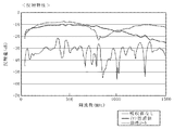
図4〜図5は、本実施の形態に係る電磁波抑制材料を用いて、高調波フィルタ効果を評価したグラフである。例えば、50MHz〜1500MHzの周波数範囲(電磁波の要求吸収性能は、特に30MHz〜1500MHzの周波数範囲)の反射量の測定結果を示している。 4 to 5 are graphs in which the harmonic filter effect is evaluated using the electromagnetic wave suppressing material according to the present embodiment. For example, the measurement results of the reflection amount in the frequency range of 50 MHz to 1500 MHz (the required absorption performance of electromagnetic waves is particularly the frequency range of 30 MHz to 1500 MHz) are shown.
細線は試料(吸収体)なしの条件での測定結果であり、実線は本実施の形態によるイオン性液体材料1を用いた条件での測定結果であり、破線は電磁波抑制シートとして市販されている磁性シート(センダスト(Fe−Al−Si)粉を樹脂で結着したもの(商品名:バスタレイド(NECトーキン社製))を用いた条件での測定結果である。 The thin line is the measurement result under the condition without the sample (absorber), the solid line is the measurement result under the condition using the ionic liquid material 1 according to the present embodiment, and the broken line is commercially available as an electromagnetic wave suppression sheet. It is a measurement result on the conditions using the magnetic sheet (The thing (Brand name: Busta Raid (made by NEC TOKIN)) which bind | concluded sendust (Fe-Al-Si) powder with resin.
図4は、マイクロストリップライン5の入力(IN)側に信号を入力した時、反射される反射特性(S11特性)を示しており、縦軸に反射量(dB)、横軸に周波数(MHz)を示す。 FIG. 4 shows reflection characteristics (S11 characteristics) that are reflected when a signal is input to the input (IN) side of the microstrip line 5. The vertical axis represents the reflection amount (dB) and the horizontal axis represents the frequency (MHz). ).
図4より、50MHz〜約1000MHzの周波数範囲においては、太線で示すゲル状材料(イオン性液体材料1)を用いたときの反射率は、−20dB〜−10dBの範囲にあり、特に約−10dB前後であって、破線で示す従来の磁性シートを用いたときの反射率と同程度又は若干低反射の特性を示している。また、細線で示す試料なし(吸収体なし)での反射率は、−60dB〜−20dBの範囲であって、特に−30dB〜−40dBの範囲で大きく上下している。 From FIG. 4, in the frequency range of 50 MHz to about 1000 MHz, the reflectivity when using the gel-like material (ionic liquid material 1) indicated by a thick line is in the range of −20 dB to −10 dB, particularly about −10 dB. It shows the characteristics of the same or slightly lower reflectivity than before and after using the conventional magnetic sheet indicated by a broken line. Further, the reflectance without the sample (without the absorber) indicated by the thin line is in the range of −60 dB to −20 dB, and particularly greatly increases and decreases in the range of −30 dB to −40 dB.
ここでの反射率−30dBとは、マイクロストリップライン5の入力側へ入力した信号(100%)に対し、入力ポートとマイクロストリップラインモデルのインピーダンスとの不整合や、試料の設置におけるインピーダンスの不整合のために、入力側へ反射される信号の反射率が0.1%となることを意味する。 Here, the reflectance of −30 dB is a mismatch between the input port and the impedance of the microstrip line model with respect to the signal (100%) input to the input side of the microstrip line 5, and the impedance of the sample is not set. For the sake of matching, this means that the reflectance of the signal reflected to the input side is 0.1%.
図4より、50MHz〜約1000MHzの周波数範囲においては、イオン性液体材料1を用いたときの反射率は、磁性シートを用いたときの反射率と同程度であり、試料なし(吸収体なし)での反射率を上回っていて、10%(反射率)程度となっている。但し、この場合、反射されない信号は90%であるので、電磁波抑制及び吸収効果の点では実質的に問題がない結果であると言える。 From FIG. 4, in the frequency range of 50 MHz to about 1000 MHz, the reflectance when using the ionic liquid material 1 is similar to the reflectance when using the magnetic sheet, and there is no sample (no absorber). It is higher than the reflectance at 10% (reflectance). However, in this case, since the signal that is not reflected is 90%, it can be said that there is substantially no problem in terms of electromagnetic wave suppression and absorption effects.
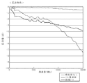
図5は、マイクロストリップライン5の入力側に信号を入力した時、信号が透過する伝送特性(S21特性)を示し、縦軸に伝送量(dB)、横軸に周波数(MHz)を示す。 FIG. 5 shows a transmission characteristic (S21 characteristic) through which a signal is transmitted when a signal is input to the input side of the microstrip line 5, a vertical axis indicates a transmission amount (dB), and a horizontal axis indicates a frequency (MHz).
図5より、50MHz〜約1000MHzの周波数範囲においては、太線で示すイオン性液体材料1を用いたときの伝送量は、破線で示す磁性シートを用いたときの伝送量や細線で示す試料なし(吸収体なし)での伝送量を下回り、伝送量が少ないので、より高いフィルタ効果を有すると言える。 From FIG. 5, in the frequency range of 50 MHz to about 1000 MHz, the transmission amount when using the ionic liquid material 1 indicated by the thick line is the transmission amount when using the magnetic sheet indicated by the broken line and no sample indicated by the thin line ( It can be said that it has a higher filter effect because the transmission amount is less than the transmission amount without the absorber) and the transmission amount is small.
図6は、マイクロストリップライン5の入力側に信号を入力した時、試料で吸収される吸収特性(損失特性)を示し、縦軸に損失率(相対値)、横軸に周波数(MHz)を示す。入力量から、図4に対応する反射量と図5に対応する透過量とを差し引いた量が損失量となる。この損失量が大きいほど、電磁波抑制及び吸収効果が大きいということになる。 FIG. 6 shows the absorption characteristics (loss characteristics) absorbed by the sample when a signal is input to the input side of the microstrip line 5, the vertical axis indicates the loss rate (relative value), and the horizontal axis indicates the frequency (MHz). Show. The amount obtained by subtracting the reflection amount corresponding to FIG. 4 and the transmission amount corresponding to FIG. 5 from the input amount is the loss amount. The larger the loss amount, the greater the electromagnetic wave suppression and absorption effect.
図6より、50MHz〜約1000MHz(特に800MHz程度)の周波数範囲においては、太線で示すイオン性液体材料1を用いたときの損失量は、一点鎖線で示すNaCl水溶液を用いたときの損失量や、破線で示す磁性シートを用いたときの損失量、細線で示す試料なし(吸収体なし)での損失量を上回っている。なお、NaCl水溶液の試料については、本出願人が既に提起した特願2005−136560に示された例を参考までに表わしたものである。 From FIG. 6, in the frequency range of 50 MHz to about 1000 MHz (particularly about 800 MHz), the loss amount when using the ionic liquid material 1 indicated by the thick line is the loss amount when using the NaCl aqueous solution indicated by the alternate long and short dash line. The loss amount when the magnetic sheet indicated by the broken line is used exceeds the loss amount without the sample (without the absorber) indicated by the thin line. In addition, about the sample of NaCl aqueous solution, the example shown by Japanese Patent Application No. 2005-136560 which this applicant has already proposed is represented for reference.
図6の測定結果より、誘電損失を用いたイオン性液体材料1は、磁気損失を用いた市販の磁性シートなどよりも、50MHz〜約1000MHz、特に800Hz以下の周波数範囲において、優れた電磁波抑制及び吸収効果を有することが分かる。 From the measurement results of FIG. 6, the ionic liquid material 1 using dielectric loss is superior in electromagnetic wave suppression and in a frequency range of 50 MHz to about 1000 MHz, particularly 800 Hz or less, than a commercially available magnetic sheet using magnetic loss. It can be seen that it has an absorption effect.
また、本実施の形態によるイオン性液体材料1は、既存の磁性シートと比較して、比重が軽く、柔軟性に優れる。 In addition, the ionic liquid material 1 according to the present embodiment has a light specific gravity and excellent flexibility as compared with an existing magnetic sheet.
また、材質が単独物からなる(即ち、媒体が不要である)ので、100%の濃度にでき、高密度に電磁波抑制材を作製することが可能であるため、使用量を少なくしても(或いは厚さを薄くしても)電磁波吸収効率が高くなり、しかも水分等の媒体の揮発等の問題がなく、耐久性に優れたものとなる。また、作製も比較的容易である。 In addition, since the material is a single material (that is, no medium is required), the concentration can be 100%, and the electromagnetic wave suppressing material can be produced at a high density. Even if the thickness is reduced, the electromagnetic wave absorption efficiency is increased, and there is no problem of volatilization of a medium such as moisture, and the durability is excellent. Moreover, the production is relatively easy.
更に、このイオン性液体材料1は、柔軟性があるため、形状追随性や可とう性に富み、例えば、電磁波を透過する樹脂フィルムなどの柔軟性のあるシート状体、柔軟性の袋状体、硬いケース状体、又は筐体等のいかなる封止材でも封止(或いは梱包)可能である。そのため、バルク状からシート状まで、形状による特性の制限がないという点においても、既存のものより優位性がある。 Furthermore, since this ionic liquid material 1 has flexibility, it is rich in shape followability and flexibility. For example, a flexible sheet-like body such as a resin film that transmits electromagnetic waves, or a flexible bag-like body. It can be sealed (or packed) with any sealing material such as a hard case or a housing. Therefore, there is an advantage over the existing one in that there is no limitation of the characteristics depending on the shape from the bulk shape to the sheet shape.
加えて、このイオン性液体材料1は、数100℃という高沸点を有し、凝固点も−20℃と低温であるため、デバイスに適用したときの使用温度範囲が広く、信頼性も高い。 In addition, since the ionic liquid material 1 has a high boiling point of several hundred degrees C. and a freezing point as low as -20 degrees C., the operating temperature range when applied to a device is wide and the reliability is high.
このように、本実施の形態によるイオン性液体又はそれを保持したゲル状材料の電磁波吸収及び抑制効果が高効率であり、電子機器からの(或いは、電子機器に対する)電磁波の影響を最小限に抑制することができ、またフレキシブル性を有し、かつ高い耐久性及び信頼性を確保したEMC対策品として有用である。 Thus, the electromagnetic wave absorption and suppression effect of the ionic liquid or the gel material holding the ionic liquid according to the present embodiment is highly efficient, and the influence of the electromagnetic wave from the electronic device (or on the electronic device) is minimized. It can be suppressed, and is useful as an EMC countermeasure product having flexibility and ensuring high durability and reliability.
これにより、不要輻射対策コストを激減できるだけでなく、高効率なために対策時間を削減することができる。 As a result, the unnecessary radiation countermeasure cost can be drastically reduced, and the countermeasure time can be reduced due to high efficiency.
また、既存の磁性材料と比較してフレキシブル性を有するために、実装面での簡易化を図れることや、幅広い用途での使用方法を実現できる。 In addition, since it has flexibility compared to existing magnetic materials, it can be simplified in terms of mounting and can be used in a wide range of applications.
更に、ゲル状であるため、基板間、もしくは基板と筐体との間への配置も可能であり、電磁波抑制及び吸収材料と衝撃緩衝材との両機能を兼ね備えた新たな材料及びデバイスとしても利用することができる。 Furthermore, since it is in the form of a gel, it can be placed between the substrates or between the substrate and the housing, and as a new material and device having both functions of electromagnetic wave suppression and absorption material and shock absorbing material Can be used.
次に、図7〜図11に、イオン性液体材料1を電子機器に適用した例を示す。 Next, FIGS. 7 to 11 show examples in which the ionic liquid material 1 is applied to an electronic device.
図7には、電子部品の実装されたA基板(プリント配線基板)11Aと電子部品の実装されたB基板(プリント配線基板)11Bとを内蔵し、更にモニタ画面12を具備するハンディカメラ10を示す。
FIG. 7 shows a
このハンディカメラ10において、イオン性液体材料1(又は電磁波抑制材)は、図8に示すように、例えば、A基板11AとB基板11Bとを電気的に接続する配線14を形成したフレキシブル配線基板13を挟持する状態で配置するために、及び、各基板上に実装されたICチップ(集積回路素子)16の上面等に貼り付けて配置するために、フィルム2で封止されたイオン性液体材料1を用いることができる。
In this
図9には、電子部品の実装されたB基板(プリント配線基板)11Bと電子部品の実装されたC基板(プリント配線基板)11Cとを内蔵し、更に筐体13とモニタ画面12とを具備するハンディカメラ10を示す。
9 includes a B board (printed wiring board) 11B on which electronic components are mounted and a C board (printed wiring board) 11C on which electronic components are mounted, and further includes a
図10(A)に示すように、例えば、B基板11Bの近傍にC基板11Cを配置する際に、図10(B)に示すように、B基板11Bの実装面とC基板11Cの非実装面との間隙に、イオン性液体材料1のみを(即ち、封止材なしで)充填して挟持することができる。また、図10(C)に示すように、B基板11Bの実装面とC基板11Cの実装面との間隙に、イオン性液体材料1のみを充填して挟持することができる。この時に、配置されるイオン性液体材料1は、それ単独であってよいが、フィルム2に封止されたものであってもよい。単独物の場合は、ゲル状であって上記間隙内に容易に充填でき、しかも実装面などの形状に良く追随することができ、両基板の接着にも有効となる。 As shown in FIG. 10A, for example, when the C substrate 11C is arranged in the vicinity of the B substrate 11B, the mounting surface of the B substrate 11B and the non-mounting of the C substrate 11C are performed as shown in FIG. It is possible to fill and sandwich only the ionic liquid material 1 (that is, without a sealing material) in the gap with the surface. Further, as shown in FIG. 10C, the gap between the mounting surface of the B substrate 11B and the mounting surface of the C substrate 11C can be filled with only the ionic liquid material 1 and sandwiched. At this time, the ionic liquid material 1 to be arranged may be alone, or may be sealed with the film 2. In the case of a single product, it is in the form of a gel and can be easily filled in the gap, and can follow the shape of the mounting surface and the like, and is effective for bonding the two substrates.
また、図11(A)に示すように、例えば、C基板11Cの近傍に筐体13が存在する場合、図11(B)に示すように、C基板11Cの実装面と筐体13との間隙に、イオン性液体材料1を挟持することができる。この時にも、配置されるイオン性液体材料1は、素材のままであってもよいし、フィルム2で封止されたものであってもよい。
Further, as shown in FIG. 11A, for example, when the
このように、イオン性液体材料1を、内的な電磁波の発生部位と、外的な電磁波の作用部位との少なくとも一方に設けることにより、電子機器に対する(或いは、電子機器からの)電磁波の影響を最小限に抑制することができる。 In this way, by providing the ionic liquid material 1 at least one of the internal electromagnetic wave generation site and the external electromagnetic wave operation site, the influence of the electromagnetic wave on the electronic device (or from the electronic device). Can be minimized.
以上、本発明を実施の形態に基づいて説明したが、本発明はこれらの例に何ら限定されるものではなく、発明の主旨を逸脱しない範囲で適宜変更可能であることは言うまでもない。 As mentioned above, although this invention was demonstrated based on embodiment, it cannot be overemphasized that this invention is not limited to these examples at all, and can be suitably changed in the range which does not deviate from the main point of invention.
本発明の電磁波抑制材及び電子機器は、電子機器の電磁波対策に適用可能である。 The electromagnetic wave suppression material and electronic device of the present invention can be applied to electromagnetic wave countermeasures for electronic devices.
1…イオン性液体材料、2…フィルム、3…ラミネート材、4、6…基板、
5…マイクロストリップライン、7…導電層、8…ネットワークアナライザ、
9a、9b…端子、10…ハンディカメラ、11A…A基板(プリント配線基板)、
11B…B基板(プリント配線基板)、11C…C基板(プリント配線基板)、
12…モニタ画面、13…フレキシブル配線基板、14…配線、15…筐体、
16…集積回路チップ、20…電磁波抑制材
DESCRIPTION OF SYMBOLS 1 ... Ionic liquid material, 2 ... Film, 3 ... Laminate material, 4, 6 ... Substrate,
5 ... microstrip line, 7 ... conductive layer, 8 ... network analyzer,
9a, 9b ... terminal, 10 ... handy camera, 11A ... A board (printed wiring board),
11B ... B board (printed wiring board), 11C ... C board (printed wiring board),
12 ... monitor screen, 13 ... flexible wiring board, 14 ... wiring, 15 ... housing,
16 ... Integrated circuit chip, 20 ... Electromagnetic wave suppression material
Claims (7)
It is formed of a gel-like material made of polyacrylamide having only an ionic liquid, the ionic liquid is composed of a cation and an anion, and the cation is composed of an aromatic system and an aliphatic quaternary ammonium salt system. An electromagnetic wave suppressing material comprising at least one selected from the group consisting of at least one selected from the group consisting of inorganic ions and fluorine-containing organic anions.
Priority Applications (1)
| Application Number | Priority Date | Filing Date | Title |
|---|---|---|---|
| JP2005208425A JP4915059B2 (en) | 2005-07-19 | 2005-07-19 | Electromagnetic wave suppressing material and electronic device |
Applications Claiming Priority (1)
| Application Number | Priority Date | Filing Date | Title |
|---|---|---|---|
| JP2005208425A JP4915059B2 (en) | 2005-07-19 | 2005-07-19 | Electromagnetic wave suppressing material and electronic device |
Publications (2)
| Publication Number | Publication Date |
|---|---|
| JP2007027470A JP2007027470A (en) | 2007-02-01 |
| JP4915059B2 true JP4915059B2 (en) | 2012-04-11 |
Family
ID=37787833
Family Applications (1)
| Application Number | Title | Priority Date | Filing Date |
|---|---|---|---|
| JP2005208425A Expired - Fee Related JP4915059B2 (en) | 2005-07-19 | 2005-07-19 | Electromagnetic wave suppressing material and electronic device |
Country Status (1)
| Country | Link |
|---|---|
| JP (1) | JP4915059B2 (en) |
Families Citing this family (7)
| Publication number | Priority date | Publication date | Assignee | Title |
|---|---|---|---|---|
| JP5452847B2 (en) * | 2007-03-22 | 2014-03-26 | スリーエム イノベイティブ プロパティズ カンパニー | Electromagnetic shielding material and sheet |
| JP4992701B2 (en) | 2007-12-19 | 2012-08-08 | ソニー株式会社 | Electromagnetic wave suppression material, electromagnetic wave suppression device, electronic equipment |
| JP5134421B2 (en) * | 2008-04-09 | 2013-01-30 | デクセリアルズ株式会社 | Electromagnetic wave suppressing material and electromagnetic wave suppressing sheet |
| JP4993380B2 (en) * | 2008-04-14 | 2012-08-08 | ソニーケミカル&インフォメーションデバイス株式会社 | Electromagnetic wave suppressor and method for producing the same |
| JP2009289986A (en) * | 2008-05-29 | 2009-12-10 | Tdk Corp | Method of manufacturing electronic component and noise countermeasure table |
| JP2010165868A (en) | 2009-01-15 | 2010-07-29 | Three M Innovative Properties Co | Gel-like composition |
| CN112029221A (en) * | 2020-09-04 | 2020-12-04 | 北京化工大学常州先进材料研究院 | Ionic gel/conductive polymer electromagnetic shielding material, preparation method and application thereof |
Family Cites Families (7)
| Publication number | Priority date | Publication date | Assignee | Title |
|---|---|---|---|---|
| JPS6468999A (en) * | 1987-09-09 | 1989-03-15 | Nok Corp | Electromagnetic wave absorbing material |
| JPH0367436A (en) * | 1989-08-03 | 1991-03-22 | Nec Corp | Exposing method for color cathode-ray tube |
| JP2772403B2 (en) * | 1990-03-16 | 1998-07-02 | 清水建設株式会社 | Structural radio wave absorber |
| JPH0521982A (en) * | 1991-07-11 | 1993-01-29 | Nec Environment Eng Ltd | Electromagneticwave absorber |
| JPH0797238A (en) * | 1993-09-27 | 1995-04-11 | Central Glass Co Ltd | Electromagnetic shield soundproof glass |
| JPH09205011A (en) * | 1996-01-24 | 1997-08-05 | Bridgestone Corp | Magnetic material |
| JP2004253640A (en) * | 2003-02-20 | 2004-09-09 | Matsushita Electric Ind Co Ltd | Electromagnetic wave absorbing material |
-
2005
- 2005-07-19 JP JP2005208425A patent/JP4915059B2/en not_active Expired - Fee Related
Also Published As
| Publication number | Publication date |
|---|---|
| JP2007027470A (en) | 2007-02-01 |
Similar Documents
| Publication | Publication Date | Title |
|---|---|---|
| JP4915059B2 (en) | Electromagnetic wave suppressing material and electronic device | |
| CN1738523B (en) | Electromagnetism suppressing material, electromagnetism suppressing device, and electronic appliance | |
| JP6213518B2 (en) | Electronics | |
| JP5452847B2 (en) | Electromagnetic shielding material and sheet | |
| JP3922039B2 (en) | Electromagnetic wave absorbing material and various products using the same | |
| JP5333776B2 (en) | Capacitance element, printed wiring board, semiconductor package, and semiconductor circuit | |
| WO2016203842A1 (en) | Electronic apparatus and antenna element | |
| JP4975743B2 (en) | Multilayer thin electromagnetic wave absorption film using surface electric resistance control | |
| JP2008270370A (en) | Electromagnetic wave shielding sheet | |
| US20180295756A1 (en) | Electromagnetic wave absorber and electronic device | |
| Kim et al. | Low‐cost and miniaturized metamaterial absorber using 3D printed swastika symbol | |
| JP2014110325A (en) | Electromagnetic wave absorber and optical transceiver | |
| JP2000013081A (en) | Electronic part | |
| JP4992701B2 (en) | Electromagnetic wave suppression material, electromagnetic wave suppression device, electronic equipment | |
| JP2010171601A (en) | Low impedance-loss line structure | |
| JP2006319048A (en) | Electromagnetic-wave suppressive material, electromagnetic-wave suppressive device, and electronic machine | |
| Wang et al. | Design and analysis of multi‐band polarisation selective metasurface | |
| JP4540493B2 (en) | Printed wiring board | |
| JP5386191B2 (en) | Electromagnetic wave absorber | |
| JP2008270714A (en) | Electromagnetic wave shielding sheet | |
| CN211982208U (en) | Circuit board | |
| CN111726976B (en) | Electromagnetic wave shielding piece, transmission line assembly and electronic packaging structure applying same | |
| WO2022107538A1 (en) | Electromagnetic wave absorbing sheet | |
| JP2007109805A (en) | Electromagnetic wave suppressing member and semiconductor device | |
| WO2023127873A1 (en) | Sheet |
Legal Events
| Date | Code | Title | Description |
|---|---|---|---|
| RD13 | Notification of appointment of power of sub attorney |
Free format text: JAPANESE INTERMEDIATE CODE: A7433 Effective date: 20070125 |
|
| A621 | Written request for application examination |
Free format text: JAPANESE INTERMEDIATE CODE: A621 Effective date: 20080623 |
|
| RD02 | Notification of acceptance of power of attorney |
Free format text: JAPANESE INTERMEDIATE CODE: A7422 Effective date: 20090528 |
|
| A977 | Report on retrieval |
Free format text: JAPANESE INTERMEDIATE CODE: A971007 Effective date: 20100820 |
|
| A131 | Notification of reasons for refusal |
Free format text: JAPANESE INTERMEDIATE CODE: A131 Effective date: 20100831 |
|
| A521 | Written amendment |
Free format text: JAPANESE INTERMEDIATE CODE: A523 Effective date: 20101001 |
|
| A131 | Notification of reasons for refusal |
Free format text: JAPANESE INTERMEDIATE CODE: A131 Effective date: 20110201 |
|
| A131 | Notification of reasons for refusal |
Free format text: JAPANESE INTERMEDIATE CODE: A131 Effective date: 20111101 |
|
| A521 | Written amendment |
Free format text: JAPANESE INTERMEDIATE CODE: A523 Effective date: 20111207 |
|
| TRDD | Decision of grant or rejection written | ||
| A01 | Written decision to grant a patent or to grant a registration (utility model) |
Free format text: JAPANESE INTERMEDIATE CODE: A01 Effective date: 20111227 |
|
| A01 | Written decision to grant a patent or to grant a registration (utility model) |
Free format text: JAPANESE INTERMEDIATE CODE: A01 |
|
| A61 | First payment of annual fees (during grant procedure) |
Free format text: JAPANESE INTERMEDIATE CODE: A61 Effective date: 20120109 |
|
| FPAY | Renewal fee payment (event date is renewal date of database) |
Free format text: PAYMENT UNTIL: 20150203 Year of fee payment: 3 |
|
| FPAY | Renewal fee payment (event date is renewal date of database) |
Free format text: PAYMENT UNTIL: 20150203 Year of fee payment: 3 |
|
| LAPS | Cancellation because of no payment of annual fees |