JP4910321B2 - Image display device and control method of image display device - Google Patents
Image display device and control method of image display device Download PDFInfo
- Publication number
- JP4910321B2 JP4910321B2 JP2005206553A JP2005206553A JP4910321B2 JP 4910321 B2 JP4910321 B2 JP 4910321B2 JP 2005206553 A JP2005206553 A JP 2005206553A JP 2005206553 A JP2005206553 A JP 2005206553A JP 4910321 B2 JP4910321 B2 JP 4910321B2
- Authority
- JP
- Japan
- Prior art keywords
- scanning
- unit
- light
- image
- control information
- Prior art date
- Legal status (The legal status is an assumption and is not a legal conclusion. Google has not performed a legal analysis and makes no representation as to the accuracy of the status listed.)
- Expired - Fee Related
Links
Images


Landscapes
- Mechanical Optical Scanning Systems (AREA)
Abstract
Description
本発明は、画像表示装置及び画像表示装置の制御方法、特に、複数の光走査部により走査されるレーザ光を用いて画像を表示する画像表示装置の技術に関する。 The present invention relates to an image display device and a method for controlling the image display device, and more particularly to a technique of an image display device that displays an image using laser light scanned by a plurality of optical scanning units.
レーザ光を走査させることで画像を表示する画像表示装置には、レーザ光を走査させる光走査部が用いられる。光走査部は、画像信号に応じて変調されたレーザ光を二次元方向へ走査させる。画像表示装置は、光走査部からのレーザ光をスクリーン等に入射させることにより画像を表示する。レーザ光の変調には、一般に、レーザ光を点灯させるパルス幅を画像信号に応じて変化させるパルス幅変調(Pulse Width Modulation、以下、「PWM」という。)が用いられる。画像の1フレームにおいて、全画素について画像信号に応じた階調を表現するためには、最小単位のパルス幅を非常に小さくする必要がある。画像の画素数を多くするほど、また、画像の階調数を多くするほど、パルス幅の最小単位はさらに小さくなる。高出力のレーザ光源は、小さいパルス幅に応じて正確かつ高速にスイッチングを行うことが非常に困難である。また、従来、複数のプロジェクタからの投写光により1つの画像を形成する画像表示装置が提案されている。画像表示装置の各プロジェクタは、スクリーン等の投写面の領域を分担して、画像信号に応じた光を投写する。この場合、各プロジェクタの解像度を合計した解像度によって1つの画像を表示することから、1つのプロジェクタを用いて画像を形成する場合に比較して、容易に高解像度な画像を得ることができる。また、明るい画像を得ることができるという利点もある。レーザ光を用いて画像を表示する画像表示装置においても、複数の光走査部により分担してレーザ光を走査させることにより、単独の光走査部を用いる場合よりも低い変調周波数で画像を表示することが可能となる。複数のプロジェクタからの投写光により1つの画像を形成する画像表示装置の技術は、例えば、特許文献1及び2に提案されている。
In an image display device that displays an image by scanning a laser beam, an optical scanning unit that scans the laser beam is used. The optical scanning unit scans the laser beam modulated according to the image signal in a two-dimensional direction. The image display device displays an image by causing laser light from an optical scanning unit to enter a screen or the like. For modulation of laser light, pulse width modulation (hereinafter referred to as “PWM”) in which the pulse width for turning on the laser light is changed in accordance with the image signal is generally used. In order to express the gradation corresponding to the image signal for all the pixels in one frame of the image, it is necessary to make the minimum unit pulse width very small. As the number of pixels of the image is increased and the number of gradations of the image is increased, the minimum unit of the pulse width is further reduced. A high-power laser light source is very difficult to switch accurately and at high speed according to a small pulse width. Conventionally, there has been proposed an image display device that forms one image by projection light from a plurality of projectors. Each projector of the image display device shares a region of a projection surface such as a screen and projects light according to an image signal. In this case, since one image is displayed with the total resolution of the projectors, it is possible to easily obtain a high-resolution image as compared with the case where an image is formed using one projector. There is also an advantage that a bright image can be obtained. Even in an image display device that displays an image using laser light, the image is displayed at a lower modulation frequency than when a single optical scanning unit is used by scanning the laser light in a shared manner by a plurality of optical scanning units. It becomes possible. For example,
従来、複数のプロジェクタを用いて画像を表示する場合、隣接する投写領域同士を重ね合わせることにより、切れ目が無い画像を形成している。投写領域同士を重ね合わせる継目部分には、画像信号に応じた変調光が重畳して投写されることから、明るさを調節することにより継目部分を目立たなくする必要がある。特許文献1にて提案される技術では、画像データを補正することにより継目部分の明るさを調節する。この場合、光量を低下させた複数の投写光を用いることから、表現可能な階調の刻みが半減し、画像信号に応じた画像を表示することが困難となる。特許文献2にて提案される技術では、遮光板を用いることにより継目部分の明るさを調節する。この場合、装置の構成が複雑となり、さらに設置も困難となる。また、いずれも技術においても、継目部分における画素のずれを正確に解消することが難しいことから、精細な画像を得ることが困難である。従って、レーザ光を用いる画像表示装置に従来の技術をそのまま適用したとしても、走査領域同士の継目部分が目立たず高品質な画像を表示することが困難であるという問題を生じる。本発明は、上述の問題に鑑みてなされたものであり、複数の光走査部を用いてビーム光の走査を分担させ、走査領域同士の継目部分が目立たない高品質な画像を表示することが可能な画像表示装置、及び画像表示装置の制御方法を提供することを目的とする。
Conventionally, when an image is displayed using a plurality of projectors, a continuous image is formed by overlapping adjacent projection areas. Since the modulated light corresponding to the image signal is projected on the joint portion where the projection areas are overlapped, it is necessary to make the joint portion inconspicuous by adjusting the brightness. In the technique proposed in
上述した課題を解決し、目的を達成するために、本発明によれば、画像信号に応じて変調されたビーム光を走査させ、ビーム光の走査領域を合成させて表示領域を形成する複数の光走査部と、表示領域に基づいて設定される画素を用いて画像を表示させるための制御情報を記憶する記憶部と、制御情報に基づいて光走査部を制御する制御部と、を有することを特徴とする画像表示装置を提供することができる。 In order to solve the above-described problems and achieve the object, according to the present invention, a plurality of light beams that are modulated according to an image signal are scanned and a scanning region of the light beams is combined to form a display region. An optical scanning unit; a storage unit that stores control information for displaying an image using pixels set based on a display region; and a control unit that controls the optical scanning unit based on the control information. An image display device characterized by the above can be provided.
本発明において、画像表示装置の表示領域は、複数の走査領域を合成させて形成される。画像は、表示領域に基づいて設定し直された画素を用いて表示される。ビーム光をラスタースキャンさせる場合、ビーム光の点灯タイミング、及び消灯タイミングを適宜設定することにより、画像を表示させる位置を容易に変更させることが可能である。ビーム光を走査させる方向を変化させることで、元の走査領域に対する表示領域の回転度も容易に変化させることができる。また、新たに設定された画素を用いて画像を表示させることも、画像信号を変換することにより可能である。このようなビーム光を用いることによる利点を利用して、複数の走査領域に跨る新たな表示領域を生成することができる。さらに、ビーム光を走査させる位置を調節することにより、複数の光走査部からのビーム光を画素単位で重畳させることができる。重畳させる部分における階調表現を複数のビーム光で分担させることで、階調の刻みを減少させることが無くなる上、重畳部分でも精細な表示を行うことができる。本発明の構成には遮光板を用いる必要が無いことから装置を簡易な構成にすることもできる。また、少なくとも走査領域同士を重畳させるように複数の光走査部を設置すれば、後は制御情報に基づく制御により表示領域に画像を表示させることが可能であるから、従来と比較して装置の設置も容易にできる。これにより、複数の光走査部を用いてビーム光の走査を分担させ、走査領域同士の継目部分が目立たない高品質な画像を表示することが可能な画像表示装置を得られる。 In the present invention, the display area of the image display device is formed by combining a plurality of scanning areas. The image is displayed using pixels that have been reset based on the display area. In the case of raster scanning of the beam light, the position for displaying the image can be easily changed by appropriately setting the lighting timing and extinguishing timing of the beam light. By changing the scanning direction of the light beam, the degree of rotation of the display area relative to the original scanning area can be easily changed. It is also possible to display an image using newly set pixels by converting the image signal. By utilizing the advantage of using such a light beam, a new display area extending over a plurality of scanning areas can be generated. Furthermore, by adjusting the position where the light beam is scanned, the light beams from the plurality of light scanning units can be superimposed on a pixel basis. By sharing the gradation expression in the overlapped portion with a plurality of light beams, the gradation step is not reduced and fine display can be performed in the overlapped portion. Since it is not necessary to use a light shielding plate in the configuration of the present invention, the apparatus can be simplified. In addition, if a plurality of optical scanning units are installed so that at least the scanning regions overlap each other, it is possible to display an image on the display region by control based on the control information. Installation is also easy. Accordingly, it is possible to obtain an image display device capable of sharing the scanning of the beam light using a plurality of optical scanning units and displaying a high-quality image in which the joint portion between the scanning regions is not conspicuous.
また、本発明の好ましい態様によれば、記憶部は、画像表示装置の外部から入力された制御情報を記憶することが望ましい。これにより、画像表示装置の外部の構成を用いて、複数の光走査部からのビーム光を画素単位で重畳させることができる。 According to a preferred aspect of the present invention, it is desirable that the storage unit stores control information input from the outside of the image display device. Thereby, it is possible to superimpose the light beams from the plurality of optical scanning units on a pixel-by-pixel basis using an external configuration of the image display device.
また、本発明の好ましい態様によれば、光走査部ごとの走査領域の位置を検知する走査位置検知部と、走査位置検知部からの出力に応じて制御情報を生成する制御情報生成部と、を有することが望ましい。これにより、画像表示装置の内部の構成を用いて、複数の光走査部からのビーム光を画素単位で重畳させることができる。 Further, according to a preferred aspect of the present invention, a scanning position detection unit that detects the position of the scanning region for each optical scanning unit, a control information generation unit that generates control information according to an output from the scanning position detection unit, It is desirable to have Thereby, it is possible to superimpose the light beams from the plurality of optical scanning units in units of pixels using the internal configuration of the image display apparatus.
また、本発明の好ましい態様としては、光走査部は、表示領域のうち走査領域同士が重畳する重畳領域において、複数の光走査部に対して分割されたパルス信号を用いて変調されたビーム光を走査させることが望ましい。これにより、階調の刻みを減少させること無く、重畳部分でも精細な表示を行うことができる。 In a preferred aspect of the present invention, the optical scanning unit includes a beam light modulated using a pulse signal divided for a plurality of optical scanning units in an overlapping region where the scanning regions overlap in the display region. It is desirable to scan. As a result, it is possible to perform fine display even in the overlapped portion without reducing gradation steps.
また、本発明の好ましい態様としては、記憶部は、走査領域に対する表示領域の回転度を示すデータを含む制御情報を記憶することが望ましい。これにより、それぞれ異なる傾きの走査領域上に表示領域を設定することができる。 As a preferred aspect of the present invention, the storage unit preferably stores control information including data indicating the degree of rotation of the display area with respect to the scanning area. Thereby, the display area can be set on the scanning area having different inclinations.
さらに、本発明によれば、走査領域の一部を互いに重畳させるように配置された複数の光走査部によりビーム光を走査させるビーム光走査工程と、光走査部ごとの走査領域の位置を検知する走査領域検知工程と、走査領域検知工程において検知された走査領域の位置から、複数の走査領域を合成させた表示領域に画像を表示させるための制御情報を生成する制御情報生成工程と、制御情報を記憶する記憶工程と、制御情報に基づいて光走査部を制御する光走査部制御工程と、を含むことを特徴とする画像表示装置の制御方法を提供することができる。制御情報生成工程において、表示領域に画像を表示させるための制御情報を生成することにより、走査領域を合成させて形成された表示領域において画像を表示させることができる。走査領域の位置情報に基づいて制御情報を生成することから、ビーム光を画素単位で重畳させ、重畳部分でも精細な表示を行うことができる。これにより、複数の光走査部を用いてビーム光の走査を分担させ、走査領域同士の継目部分が目立たない高品質な画像を表示することができる。 Furthermore, according to the present invention, a light beam scanning step of scanning a light beam by a plurality of light scanning units arranged so that a part of the scanning region overlaps each other, and a position of the scanning region for each light scanning unit are detected. A scanning area detecting step, a control information generating step for generating control information for displaying an image in a display area obtained by combining a plurality of scanning areas from the position of the scanning area detected in the scanning area detecting step, and a control It is possible to provide a method for controlling an image display device, including a storage step for storing information and an optical scanning unit control step for controlling the optical scanning unit based on the control information. In the control information generation step, by generating control information for displaying an image in the display area, the image can be displayed in the display area formed by combining the scanning areas. Since the control information is generated based on the position information of the scanning region, it is possible to superimpose the beam light in units of pixels and perform fine display even in the superimposed portion. Thereby, it is possible to share the scanning of the light beam using a plurality of optical scanning units, and display a high-quality image in which the joint portion between the scanning regions is not conspicuous.
また、本発明の好ましい態様としては、制御情報生成工程において、走査領域に対する表示領域の回転度、光走査部によるビーム光の走査を開始させる位置、及びビーム光の走査を終了させる位置を示すデータを含む制御情報を生成することが望ましい。走査領域に対する表示領域の回転度を示すデータを制御情報に含めることにより、それぞれ異なる傾きの走査領域上に表示領域を設定することができる。また、ビーム光の走査を開始させる位置、及び走査を終了させる位置を示すデータを制御情報に含めることにより、走査領域上に表示領域を設定することができる。 Further, as a preferred aspect of the present invention, in the control information generation step, data indicating the degree of rotation of the display area with respect to the scanning area, the position where the light scanning unit starts scanning the light beam, and the position where the scanning of the light beam ends. It is desirable to generate control information including By including data indicating the degree of rotation of the display area with respect to the scan area in the control information, the display area can be set on the scan area having different inclinations. In addition, the display area can be set on the scanning area by including in the control information data indicating the position where the scanning of the light beam starts and the position where the scanning ends.
以下に図面を参照して、本発明の実施例を詳細に説明する。 Embodiments of the present invention will be described below in detail with reference to the drawings.
図1は、本発明の実施例に係る画像表示装置100の設置例を示す。画像表示装置100は、X方向に並列された第1光走査部101、及び第2光走査部102を有する。第1光走査部101、及び第2光走査部102は、観察者側に設けられたスクリーン110にレーザ光を供給し、スクリーン110で反射する光を観察することで画像を鑑賞する、いわゆるフロント投写型プロジェクタである。
FIG. 1 shows an installation example of an
図2は、第1光走査部101の概略構成を示す。光源装置111は、ビーム光であるレーザ光を供給する。光源装置111からのレーザ光は、照明光学系112を透過した後、スキャナ115に入射する。スキャナ115は、光源装置111からのレーザ光を二次元方向へ走査させる。
FIG. 2 shows a schematic configuration of the first
図3は、光源装置111の概略構成を示す。光源装置111は、赤色レーザ光(以下、「R光」という。)を供給するR光用光源部121Rと、緑色レーザ光(以下、「G光」という。)を供給するG光用光源部121Gと、青色レーザ光(以下、「B光」)という。)を供給するB光用光源部121Bと、を有する。R光用光源部121Rは、R光を供給する半導体レーザである。B光用光源部121Bは、B光を供給する半導体レーザである。
FIG. 3 shows a schematic configuration of the
G光用光源部121Gは、半導体レーザ122と、波長変換素子123とを有する。波長変換素子123としては、例えば、非線形光学結晶を備えるSHG(second harmonic generation)素子を用いることができる。G光用光源部121Gは、半導体レーザ122からのレーザ光を、波長変換素子123により2分の1の波長のレーザ光に変換して出射させる。G光用光源部121Gは、例えば、1040ナノメートルにピークを有する波長スペクトルの半導体レーザ122を用いることで、520ナノメートルにピークを有する波長スペクトルのG光を供給する。
The light source unit for G light 121G includes a
G光用光源部121Gは、波長変換素子123を用いることにより、容易に入手が可能な汎用の半導体レーザ122を用いることが可能となる。G光用光源部121Gは、G光を供給するものであれば良く、上述のものに限られない。G光用光源部121Gは、例えば、DPSS(Diode Pumped Solid State)レーザ発振器を用いることとしても良い。DPSSレーザ発振器は、レーザ光源からのレーザ光を用いて固体結晶を励起することにより、レーザ光を供給するものである。
The
各色光用光源部121R、121G、121Bは、それぞれ画像信号に応じて変調されたレーザ光を供給する。画像信号に応じた変調には、例えば、PWMが用いられる。光源装置111には、2つのダイクロイックミラー部124、125が設けられている。ダイクロイックミラー部124は、R光を透過し、G光を反射する。ダイクロイックミラー部125は、R光及びG光を透過し、B光を反射する。R光用光源部121RからのR光は、ダイクロイックミラー部124、125を透過した後、光源装置111から出射する。
Each color
G光用光源部121GからのG光は、ダイクロイックミラー部124で反射することにより、光路が略90度折り曲げられる。ダイクロイックミラー部124で反射したG光は、ダイクロイックミラー部125を透過した後、光源装置111から出射する。B光用光源部121BからのB光は、ダイクロイックミラー部125で反射することにより、光路が略90度折り曲げられる。ダイクロイックミラー部125で反射したB光は、光源装置111から出射する。光源装置111は、このようにして、画像信号に応じて変調されたR光、G光、B光を供給する。
The G light from the G
図4は、スキャナ115の概略構成を示す。スキャナ115は、反射ミラー202と、反射ミラー202の周囲に設けられた外枠部204とを有する、いわゆるジンバル構造をなしている。外枠部204は、回転軸であるトーションばね206によって、不図示の固定部に連結されている。外枠部204は、トーションばね206の捩れと、元の状態への復元とを利用して、トーションばね206を中心として回動する。反射ミラー202は、トーションばね206に略直交する回転軸であるトーションばね207によって、外枠部204に連結されている。反射ミラー202は、光源装置111からのレーザ光を反射する。反射ミラー202は、高反射性の部材、例えばアルミニウムや銀等の金属薄膜を形成することにより構成できる。
FIG. 4 shows a schematic configuration of the
反射ミラー202は、トーションばね207の捩れと、元の状態への復元とを利用して、トーションばね207を中心として回動する。反射ミラー202は、トーションばね207を中心として回動することにより、反射ミラー202で反射したレーザ光を第1の方向、例えば水平方向へ走査するように変位する。反射ミラー202は、外枠部204がトーションばね206を中心として回動することにより、レーザ光を第2の方向、例えば垂直方向へ走査するように変位する。また、このように、スキャナ115は、光源装置111からのレーザ光を第1の方向と第2の方向へ走査させる。
The
図5は、スキャナ115を駆動するための構成を説明するものである。反射ミラー202がレーザ光を反射する側を表側とすると、第1の電極301、302は、外枠部204の裏側の空間であって、トーションばね206に関して略対称な位置にそれぞれが設けられている。第1の電極301、302に電圧を印加すると、第1の電極301、302と、外枠部204との間には、電位差に応じた所定の力、例えば静電力が発生する。外枠部204は、第1の電極301、302に交互に電圧を印加することにより、トーションばね206を中心として回動する。
FIG. 5 illustrates a configuration for driving the
トーションばね207は、詳細には、第1のトーションばね307と第2のトーションばね308とで構成されている。第1のトーションばね307と第2のトーションばね308との間には、ミラー側電極305が設けられている。ミラー側電極305の裏側の空間には、第2の電極306が設けられている。第2の電極306に電圧を印加すると、第2の電極306とミラー側電極305との間には、電位差に応じた所定の力、例えば静電力が発生する。第2の電極306のいずれにも同位相の電圧を印加すると、反射ミラー202は、トーションばね207を中心として回動する。スキャナ115は、このようにして反射ミラー202を回動させることで、レーザ光を二次元方向へ走査させる。スキャナ115は、例えば、MEMS(Micro Electro Mechanical Systems)技術により作成することができる。
Specifically, the
スキャナ115は、例えば画像の1フレーム期間において、第2の方向へ1回レーザ光を走査させる間に、第1の方向について複数回レーザ光を往復させるように反射ミラー202を変位させる。このように、スキャナ115は、第1の方向へレーザ光を走査する周波数が、第2の方向へレーザ光を走査する周波数に比べて高くなるように駆動される。なお、第1の方向へのレーザ光の走査を高速に行うために、スキャナ115は、トーションばね207を中心として反射ミラー202を共振させる構成とすることが望ましい。反射ミラー202を共振させることにより、反射ミラー202の変位量を増大させることができる。反射ミラー202の変位量を増大させることにより、スキャナ115は、少ないエネルギーで効率良くレーザ光を走査することができる。なお、反射ミラー202は、共振を用いず駆動することとしても良い。
The
なお、スキャナ115は、電位差に応じた静電力によって駆動する構成に限られない。例えば、圧電素子の伸縮力や電磁力を用いて駆動する構成であっても良い。レーザ光を走査させる構成としては、二次元方向へレーザ光を走査させるスキャナ115に限らず、第1の方向にレーザ光を走査する反射ミラーと、第2の方向にレーザ光を走査する反射ミラーとを設ける構成としても良い。さらに、ジンバル構造を持ったスキャナ115に代えて、複数のミラー片を有する回転体を回転させるポリゴンミラーを用いても良い。
Note that the
図2に戻って、スキャナ115からのレーザ光は、投写光学系113を透過した後、スクリーン110に入射する。照明光学系112、及び投写光学系113は、光源装置111からのレーザ光をスクリーン110上に結像させる。第2光走査部102は、第1光走査部101と同様の構成を有する。なお、第1光走査部101、第2光走査部102は、各色光について1つのレーザ光を走査させる構成に限られず、各色光について複数のレーザ光を走査させる構成としても良い。
Returning to FIG. 2, the laser light from the
図6は、第1光走査部101、第2光走査部102からのレーザ光の光路を説明するものである。スキャナ115の周辺には、検出用光源部611及び走査位置検出部612が設けられている。検出用光源部611及び走査位置検出部612は、第1光走査部101、第2光走査部102のいずれに対しても設けられている。検出用光源部611及び走査位置検出部612は、スキャナ115が光源装置111からのレーザ光を反射させる側とは反対側の空間に設けられている。走査位置検出部612は、反射ミラー202(図4参照)で反射した検出用光源部611からの検出光により、二次元方向におけるスキャナ115の変位を検出する。走査位置検出部612からの出力により、スクリーン110におけるレーザ光の位置を検知することができる。なお、反射ミラー202のうち少なくとも検出光が入射する部分に、表面と同様に高反射性の部材を形成しても良い。高反射性の部材で検出光を反射する構成とすることにより、走査位置検出部612にてS/N比が高い信号を得ることができる。
FIG. 6 illustrates the optical path of laser light from the first
撮像装置620及び制御情報生成部630は、画像表示装置100の外部に設置されている。撮像装置620は、スクリーン110で反射した光を検出することにより光走査部101、102ごとの走査領域の位置を検知する走査領域検知部である。制御情報生成部630は、走査領域検知部である撮像装置620からの出力に応じて各光走査部101、102を制御する制御情報を生成する。
The
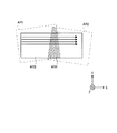
図7は、スクリーン110における第1光走査部101からのレーザ光の第1走査領域AR1、第2光走査部102からのレーザ光の第2走査領域AR2、及び画像表示装置100の表示領域AR3を示すものである。第1走査領域AR1は、第1光走査部101によってレーザ光を走査させることが可能な領域である。第2走査領域AR2は、第2光走査部101によってレーザ光を走査させることが可能な領域である。第1光走査部101、第2光走査部102は、画像表示装置100を設置する際に、第1走査領域AR1と第2走査領域AR2とを互いに重畳させるように配置される。
FIG. 7 shows a first scanning area AR1 of the laser light from the first
画像表示装置100の表示領域AR3は、第1走査領域AR1と第2走査領域AR2とを合成させることにより形成される。表示領域AR3のうち、第1走査領域AR1のみと重なり合う領域では、第1光走査部101からのレーザ光を用いて画像を表示する。表示領域AR3のうち、第2走査領域AR2のみと重なり合う領域では、第2光走査部102からのレーザ光を用いて画像を表示する。表示領域AR3のうち、第1走査領域AR1、第2走査領域AR2のいずれも重なり合う重畳領域AR4では、第1光走査部101からのレーザ光と第2光走査部102からのレーザ光とを用いて画像を表示する。表示領域AR3に表示される画像の画素は、表示領域AR3に基づいて設定し直される。
The display area AR3 of the
図示するように、第1光走査部101、第2光走査部102は、第1走査領域AR1の一部と第2走査領域AR2の一部を重畳させて配置すれば良く、第1走査領域AR1、第2走査領域AR2が互いに異なる傾きで重なり合うように配置しても良い。本実施例では、水平方向であるX方向、及び垂直方向であるY方向へ画素を配列させた表示領域AR3を、いずれも表示領域AR3に対して傾けられた第1走査領域AR1、第2走査領域AR2により合成する。
As shown in the drawing, the first
図8は、画像表示装置100により画像を表示するための構成を示す。例えば、外部の映像信号出力機器であるPC等からの画像情報信号は、第1光走査部101の制御部713、及び第2光走査部102の制御部713に入力される。撮像装置620で検知された走査領域AR1、AR2の位置に関するデータは、制御情報生成部630に入力される。制御情報生成部630は、撮像装置620の出力に応じて、制御情報を生成する。
FIG. 8 shows a configuration for displaying an image by the
図9は、第1光走査部101を制御するための構成を示すものである。画像信号入力部711は、入力端子から入力された画像信号の特性補正や増幅等を行う。また、画像信号入力部711は、例えば、アナログ式の画像信号を、ディジタル式の光源変調用パルス信号に変換する。同期/画像分離部712は、画像信号入力部711からの信号を、R光、G光、B光のそれぞれについての画像情報信号、垂直同期信号、水平同期信号に分離し、制御部713へ出力する。制御部713は、画像情報をフレームごとの情報に分けて、記憶部714へ出力する。また、記憶部714は、表示領域AR3に基づいて設定される画素を用いて画像を表示させるための制御情報を記憶する。制御情報生成部630からの制御情報には、走査領域AR1、AR2に対する表示領域AR3の回転度、光走査部101、102によるレーザ光の走査を開始させる位置、及びレーザ光の走査を終了させる位置を示すデータが含まれる。
FIG. 9 shows a configuration for controlling the first
図10は、第1走査領域AR1に対する表示領域AR3の回転度について説明するものである。第1光走査部101は、本来、第1の方向であるxa方向と、第2の方向であるya方向とにレーザ光を走査させる構成であるとする。これに対して、表示領域AR3では、第1の方向をX方向、第2の方向をY方向としてレーザ光を走査させる必要がある。X方向は、xa方向を基準としてマイナスθaだけ回転させた方向である。第1走査領域AR1に対する表示領域AR3の回転度は、マイナスθaであるとされる。
FIG. 10 illustrates the degree of rotation of the display area AR3 with respect to the first scanning area AR1. The first
図11は、第2走査領域AR2に対する表示領域AR3の回転度について説明するものである。第2光走査部102は、本来、第1の方向であるxb方向と、第2の方向であるyb方向とにレーザ光を走査させる構成であるとする。これに対して、表示領域AR3では、第1の方向をX方向、第2の方向をY方向としてレーザ光を走査させる必要がある。X方向は、xb方向を基準としてプラスθbだけ回転させた方向である。第2走査領域AR2に対する表示領域AR3の回転度は、プラスθbであるとされる。
FIG. 11 illustrates the degree of rotation of the display area AR3 with respect to the second scanning area AR2. The second
図12は、第1走査領域AR1と第2走査領域AR2との合成による表示領域AR3の形成について説明するものである。第1光走査部101は、第1走査領域AR1における本来の走査方向からマイナスθaだけ回転させたX方向とY方向とへレーザ光を走査させる。第2光走査部102は、第2走査領域AR2における本来の走査方向からプラスθbだけ回転させたX方向とY方向とへレーザ光を走査させる。
FIG. 12 illustrates the formation of the display area AR3 by combining the first scanning area AR1 and the second scanning area AR2. The first
第1走査領域AR1内における第2走査領域AR2の境界線L1上の画素Pは、境界線L1上の画素Pへレーザ光を完全に入射させることが可能な第1光走査部101からのレーザ光を用いて形成される。第2走査領域AR2内における第1走査領域AR1の境界線L2上の画素Pは、境界線L2上の画素Pへレーザ光を完全に入射させることが可能な第2光走査部102からのレーザ光を用いて形成される。従って、表示領域AR3のうち、第1走査領域AR1内の画素P、及び境界線L1上の画素Pは、第1光走査部101からのレーザ光のみを用いて形成される。表示領域AR3のうち、第2走査領域AR2内の画素P、及び境界線L2上の画素Pは、第2光走査部102からのレーザ光のみを用いて形成される。また、重畳領域AR4のうち境界線L1、境界線L2のいずれにも重ならない、ハッチングを付して示す画素Pは、第1光走査部101からのレーザ光と、第2光走査部102からのレーザ光とを用いて形成される。このようにして、光走査部101、102によるレーザ光の走査を開始させる位置、及びレーザ光の走査を終了させる位置が決定される。
The pixel P on the boundary line L1 of the second scanning area AR2 in the first scanning area AR1 is a laser from the first
図13は、第1光走査部101からのレーザ光と、第2光走査部102からのレーザ光とを用いた画素Pの形成について説明するものである。例えば、重畳領域AR4のある画素Pの階調を表現するために信号S3が生成されるとする。信号S3のパルスは、第1光走査部101からレーザ光を供給させる信号S1と、第2光走査部102からレーザ光を供給させる信号S2とに分別される。このように、各光走査部101、102は、重畳領域AR4において、各光走査部101、102に対して分割されたパルス信号を用いてレーザ光を変調する。信号S1に基づく第1光走査部101からのレーザ光と、信号S2に基づく第2光走査部102からのレーザ光とにより、信号S3に基づいて1台の光走査部からレーザ光を走査させる場合と同じように画素Pを形成することができる。
FIG. 13 illustrates the formation of the pixel P using the laser light from the first
なお、図13に示すように信号S3のパルスを交互に分別させる場合に限られず、他の手法を用いてパルスを分別することとしても良い。このようにして決定された制御情報を用いることにより、走査領域AR1、AR2を合成させて表示領域AR3を形成することができる。画像信号に応じたレーザ光の変調にはPWMを用いる場合に限られず、振幅変調を用いても良い。振幅変調を用いる場合、画素Pの階調を表現するための信号S3の振幅を、第1光走査部101に対する信号S1と、第2光走査部102に対する信号S2とに分割することにより、表示領域AR3を形成することができる。
In addition, as shown in FIG. 13, it is not restricted to the case where the pulse of signal S3 is separated alternately, It is good also as dividing a pulse using another method. By using the control information determined in this way, the display area AR3 can be formed by combining the scan areas AR1 and AR2. The modulation of the laser light according to the image signal is not limited to using PWM, and amplitude modulation may be used. When amplitude modulation is used, display is performed by dividing the amplitude of the signal S3 for expressing the gradation of the pixel P into a signal S1 for the first
重畳領域AR4における第1光走査部101、第2光走査部102の分担を決定するために、第1光走査部101からのレーザ光と第2光走査部102からのレーザ光とを重複させる画素Pの個数や位置を決定する必要がある。撮像装置620は、走査領域AR1、AR2が重なり合う状態を、画素を識別可能な精度で検知する必要がある。撮像装置620は、走査領域AR1、AR2の全体の位置を検知した後、重畳領域AR4においては画素を識別できる精度にまでズームさせて走査領域AR1、AR2を検知させることとしても良い。
In order to determine the sharing of the first
図9に戻って、制御部713は、記憶部714に記憶された制御情報に基づいて光走査部101を制御する。画像処理部721は、垂直同期信号、水平同期信号、及び記憶部714から読み出した制御情報に基づいて、スキャナ115を駆動する駆動信号を生成する。走査駆動部715は、制御部713からの駆動信号に応答してスキャナ115を駆動する。
Returning to FIG. 9, the
走査位置検出部612は、反射ミラー202の変位からスクリーン110におけるレーザ光の位置を検知し、走査位置情報を制御部713へ出力する。また、走査位置検出部612は、レーザ光をX方向へ走査させる反射ミラー202の振り角、及びレーザ光をY方向へ走査させる反射ミラー202の振り角を検出する。走査位置検出部612は、反射ミラー202をY方向へ走査させる振り角からフレーム開始信号F_Sync、反射ミラー202をX方向へ走査させる振り角からライン開始信号L_Syncをそれぞれ生成し、制御部713へ出力する。
The scanning
走査制御部723は、走査位置検出部612からの走査位置情報に基づいて、スキャナ115をフィードバック制御する。これにより、スキャナ115を正確に駆動させることができる。制御部713は、フレーム開始信号F_Sync、ライン開始信号L_Syncから演算された線速、及び垂直同期信号、水平同期信号に基づいて、画素タイミングクロックを生成する。画素タイミングクロックは、レーザ光が各画素上を通るタイミングを知るための信号であって、画像信号に応じて変調されたレーザ光を正確な位置に入射させるためのものである。
The
画像処理部721は、記憶部714から読み出された制御情報に基づいて、フレームごとの画像情報信号を変換させる。光源制御部722は、画像処理部721で変換された1フレームごとの画像情報信号を出力する。R光源駆動部732Rは、光源制御部722からの駆動信号に基づいて、R光用光源部121Rを駆動させる。G光源駆動部732Gは、光源制御部722からの駆動信号に基づいて、G光用光源部121Gを駆動させる。B光源駆動部732Bは、光源制御部722からの駆動信号に基づいて、B光用光源部121Bを駆動させる。このようにして、第1光走査部101からのレーザ光、及び第2光走査部102からのレーザ光を用いて、表示領域AR3に画像を表示することができる。
The
レーザ光をラスタースキャンさせる光走査部101、102を用いることで、レーザ光の点灯タイミング、及び消灯タイミングを適宜設定することにより、画像を表示させる位置を容易に変更させることが可能である。レーザ光を走査させる方向を変化させることで、元の走査領域AR1、AR2に対する表示領域AR3の回転度も容易に変化させることもできる。また、新たに設定された画素を用いて画像を表示させることも、画像信号を変換することにより行うことができる。このようなレーザ光を用いることによる利点を利用して、複数の走査領域AR1、AR2に跨る新たな表示領域AR3を生成することができる。
By using the
レーザ光を走査させる位置を調節することにより、複数の光走査部101、102からのレーザ光を画素単位で重畳させることができる。重畳させる部分における階調表現を複数のレーザ光で分担させることで、階調の刻みを減少させることが無くなる上、重畳部分でも精細な表示を行うことができる。本発明の構成には遮光板を用いる必要が無いことから装置を簡易な構成にできる。また、少なくとも走査領域AR1、AR2同士を重畳させるように複数の光走査部101、102を設置すれば、後は制御情報に基づく制御により表示領域AR3に画像を表示させることが可能であるから、従来と比較して装置の設置も容易にできる。これにより、複数の光走査部を用いてビーム光の走査を分担させ、走査領域同士の継目部分が目立たない高品質な画像を表示することができるという効果を奏する。
By adjusting the position where the laser light is scanned, the laser light from the plurality of
各光走査部101、102は、アナログ信号である画像信号をディジタル式の光源変調用パルス信号に変換する構成に限られない。例えば、画像信号入力部711は、ディジタル信号である画像信号をアナログ式の光源変調用強度信号に変換することとしても良い。また、画像信号入力部711は、ディジタル信号である画像信号を、ディジタル式の光源変調用パルス信号に変換することとしても良い。
Each of the
図14は、各光走査部101、102を制御する工程のフローチャートを示す。ステップS11において、走査領域の一部を互いに重畳させるように第1光走査部101及び第2光走査部102を設置する。次に、ステップS12において、第1光走査部101からのレーザ光を第1走査領域AR1の全面に走査させ、撮像装置620により第1走査領域AR1を検知する。また、ステップS13において、第2光走査部102からのレーザ光を第2走査領域AR2の全面に走査させ、撮像装置620により第2走査領域AR2を検知する。ステップS12、13は、各光走査部101、102によりレーザ光を走査させるビーム光走査工程、及び光走査部101、102ごとの走査領域AR1、AR2の位置を検知する走査領域検知工程である。
FIG. 14 shows a flowchart of a process for controlling the
次に、ステップS14において、制御情報生成部630で制御情報を生成する。ステップS14は、走査領域AR1、AR2の位置から、表示領域AR3に基づいて設定される画素を用いて画像を表示させるための制御情報を生成する制御情報生成工程である。記憶工程であるステップS15では、制御情報生成部630で生成された制御情報を記憶部714に記憶させる。そして、光走査部制御工程であるステップS16において、記憶部714から読み出された制御情報に基づいてスキャナ115及び各色光用光源部を駆動させることにより、各光走査部101、102を制御する。
Next, in step S <b> 14, the control
一度位置決めした後各光走査部101、102を移動させないのであれば、制御情報生成部630により一度生成された制御情報を用いて各光走査部101、102を制御すれば良い。このため、各光走査部101、102を一度設置した後は撮像装置620及び制御情報生成部630を不要とし、記憶部714に記憶された制御情報を用いて各光走査部101、102を制御することができる。また、各光走査部101、102を固定させる固定部を用いることとしても良い。この場合、例えば、画像表示装置100の出荷時に記憶された制御情報を用いて各光走査部101、102を制御することとしても良い。
If the
さらに、各光走査部101、102のいずれか一方に撮像装置620及び制御情報生成部630を内蔵させることとしても良い。この場合、第1光走査部101、又は第2光走査部102を移動させるごとに、外部の機器を用いること無く制御情報を生成させることができる。撮像装置620及び制御情報生成部630は、第1光走査部101、第2光走査部102の双方に内蔵させても良い。この場合、各光走査部101、102に設けられた撮像装置620からの出力を演算することで制御情報を生成することも可能である。
Furthermore, the
なお、本発明の画像表示装置は、X方向に並列された2つの光走査部101、102を備える構成に限られない。光走査部は、2つ以上を並列させても良く、Y方向等の他の方向へ並列させても良い。さらに、図15に示す画像表示装置1500のように、複数の光走査部をアレイ状に配列させても良い。画像表示装置1500は、4つの光走査部101、102、103、104を、X方向へ2つ、及びY方向へ2つ配列している。各光走査部は、互いにレーザ光の走査領域を重ね合わせるように配置されている。
The image display apparatus according to the present invention is not limited to the configuration including the two
画像表示装置1500の場合も、上記の画像表示装置100と同様に制御することにより、走査領域同士の継目部分が目立たない高品質な画像を表示することができる。なお、画像表示装置1500により画像を表示する場合、2つの走査領域が重畳する部分のほか、4つの走査領域が重畳する部分が生じる。4つの走査領域が重畳する部分については、4つの光走査部101、102、103、104からのレーザ光を用いて階調を表現するように、制御情報が生成される。
In the case of the
図16は、本実施例の変形例による表示領域の形成について説明するものである。本変形例では、第1走査領域AR1と第2走査領域AR2とが、互いにY方向の位置が一致していることを特徴とする。この場合、第1走査領域AR1及び第2走査領域AR2を合わせた全ての領域を表示領域とすることができる。本変形例では、表示領域の画素は、Y方向については第1走査領域AR1の画素、第2走査領域AR2の画素をそのまま適用し、X方向のみについて画素を設定し直す例を説明する。 FIG. 16 explains the formation of a display area according to a modification of the present embodiment. The present modification is characterized in that the first scanning area AR1 and the second scanning area AR2 have the same position in the Y direction. In this case, all the areas including the first scanning area AR1 and the second scanning area AR2 can be used as the display area. In this modification, an example will be described in which the pixels in the display area are applied as they are in the first scanning area AR1 and the pixels in the second scanning area AR2 in the Y direction, and the pixels are reset only in the X direction.
図17は、本変形例の表示領域におけるX方向の画素の設定について説明するものである。例えば、撮像装置620の出力により、第1走査領域AR1の画素Paと第2走査領域AR2の画素Pbとが、重畳領域AR4において、X方向について互いに2分の1画素分だけずれていることが検知されたとする。この場合、制御情報生成部630は、プラスX向きに2分の1画素分だけシフトさせるように第2光走査部102からの画素Pbを設定し直す。画素Paと画素Pbの位置を一致させた後、撮像装置からの出力により重畳する画素の個数を認識する。そして、2つの光走査部からのレーザ光を用いて重畳領域AR4内の画素を表示させるような制御情報を生成する。図中、黒塗りを付すように、理論上第2走査領域AR2で表示可能な画素が左右合わせて1画素少なくなるが、画像への影響は無視することができる。
FIG. 17 illustrates the setting of pixels in the X direction in the display area of this modification. For example, the pixel Pa of the first scanning area AR1 and the pixel Pb of the second scanning area AR2 may be shifted from each other by a half pixel in the X direction in the overlap area AR4 due to the output of the
本変形例は、第1走査領域AR1を基準として第2光走査部102からの画素Pbを設定し直すこととしているが、第2走査領域AR2を基準として第1光走査部101からの画素Paを設定し直すこととしても良い。また、画素をプラスX方向へシフトさせる場合に限らず、マイナスX向きにシフトさせても良い。画素Paと画素Pbとのずれは、X方向に関して最大2分の1画素分生じる。2分の1画素より小さいずれを生じる場合は、本変形例と同様にして制御情報を生成することができる。また、X方向に関して画素のずれが生じていない場合は、画素のシフトを行うこと無く、制御情報を生成する。
In this modification, the pixel Pb from the second
さらに、図18に示すように、重畳領域AR4中の一部の領域AR5において画素Pa、画素PbのX方向への幅を小さくさせることにより、画素Paと画素Pbの位置を一致させることとしても良い。制御情報生成部630は、領域AR5のX方向への幅を小さくさせるように、画素Pa、Pbを設定する。さらに、画素Pbを、画素Paの位置に一致させるようにシフトさせる。この場合、画像への影響をできるだけ少なくするように、領域AR5のX方向への幅や、画素の幅を小さくさせる度合いを適宜設定することができる。
Furthermore, as shown in FIG. 18, in the partial area AR5 in the overlapping area AR4, the positions of the pixel Pa and the pixel Pb may be matched by reducing the width of the pixel Pa and the pixel Pb in the X direction. good. The control
なお、上記各実施例において、各色光用光源部にはレーザ光を供給する半導体レーザを用いる構成としているが、ビーム光を供給可能な構成であれば、これに限られない。例えば、各色光用光源部には、面発光レーザや固体レーザ、発光ダイオード素子(LED)等の固体発光素子のほか、液体レーザやガスレーザを用いる構成としても良い。 In each of the above-described embodiments, a semiconductor laser that supplies laser light is used for each color light source unit. However, the present invention is not limited to this as long as beam light can be supplied. For example, the light source section for each color light may be configured to use a liquid laser or a gas laser in addition to a solid light emitting element such as a surface emitting laser, a solid laser, and a light emitting diode element (LED).
以上のように、本発明に係る画像表示装置は、大型かつ高品質な画像を表示する場合に有用である。 As described above, the image display device according to the present invention is useful when displaying a large and high-quality image.
100 画像表示装置、101 第1光走査部、102 第2光走査部、110 スクリーン、111 光源装置、112 照明光学系、113 投写光学系、115 スキャナ、121R R光用光源部、121G G光用光源部、121B B光用光源部、122 半導体レーザ、123 波長変換素子、124、125 ダイクロイックミラー部、202 反射ミラー、204 外枠部、206 トーションばね、207 トーションばね、301、302 第1の電極、305 ミラー側電極、306 第2の電極、307 第1のトーションばね、308 第2のトーションばね、611 検出用光源部、612 走査位置検出部、620 撮像装置、630 制御情報生成部、AR1 第1走査領域、AR2 第2走査領域、AR3 表示領域、AR4 重畳領域、711 画像信号入力部、712 同期/画像分離部、713 制御部、714 記憶部、715 走査駆動部、721 画像処理部、722 光源制御部、723 走査制御部、732R R光源駆動部、732G G光源駆動部、732B B光源駆動部、L1、L2 境界線、P 画素、1500 画像表示装置、103、104 光走査部、AR5 領域、Pa、Pb 画素 DESCRIPTION OF SYMBOLS 100 Image display apparatus, 101 1st light scanning part, 102 2nd light scanning part, 110 screen, 111 light source device, 112 Illumination optical system, 113 Projection optical system, 115 Scanner, 121R R light source part, For 121G G light Light source unit, 121B light source unit for B light, 122 semiconductor laser, 123 wavelength conversion element, 124, 125 dichroic mirror unit, 202 reflection mirror, 204 outer frame unit, 206 torsion spring, 207 torsion spring, 301, 302 first electrode 305, mirror side electrode, 306 second electrode, 307 first torsion spring, 308 second torsion spring, 611 light source for detection, 612 scanning position detector, 620 imaging device, 630 control information generator, AR1 first 1 scan area, AR2 second scan area, AR3 display area, AR Superimposition area, 711 image signal input unit, 712 synchronization / image separation unit, 713 control unit, 714 storage unit, 715 scan drive unit, 721 image processing unit, 722 light source control unit, 723 scan control unit, 732R R light source drive unit, 732G G light source driving unit, 732B B light source driving unit, L1, L2 boundary line, P pixel, 1500 image display device, 103, 104 optical scanning unit, AR5 area, Pa, Pb pixel
Claims (6)
前記表示領域に基づいて設定される画素を用いて画像を表示させる制御情報を記憶する記憶部と、
前記制御情報に基づいて前記光走査部を制御する制御部と、を有し、
前記光走査部は、前記表示領域のうち前記走査領域が重畳しない非重畳領域において、単独の前記光走査部に対して第1のパルス信号を用いて変調した前記ビーム光を走査し、前記表示領域のうち前記走査領域同士が重畳する重畳領域において、複数の前記光走査部に対して前記第1のパルス信号を分割したパルス信号を用いて変調した前記ビーム光を走査することを特徴とする画像表示装置。 A plurality of optical scanning units that scan a light beam modulated in accordance with an image signal and combine the scanning region of the light beam to form a display region;
A storage unit for storing control information for displaying an image using pixels set based on the display area;
A control unit that controls the optical scanning unit based on the control information,
The optical scanning unit scans the beam light modulated by using a first pulse signal with respect to the single optical scanning unit in a non-overlapping region where the scanning region does not overlap in the display region, and the display in the overlapping region where the scanning region to each other overlaps in the region, characterized by scanning the beam light modulated by using a pulse signal obtained by dividing the first pulse signal to a plurality of the optical scanning unit An image display device.
前記走査領域検知部からの出力に応じて前記制御情報を生成する制御情報生成部と、を有することを特徴とする請求項1に記載の画像表示装置。 A scanning region detection unit that detects the position of the scanning region for each of the optical scanning units;
The image display apparatus according to claim 1, further comprising: a control information generation unit that generates the control information in accordance with an output from the scanning region detection unit.
前記光走査部ごとの前記走査領域の位置を検知する走査領域検知工程と、
前記走査領域検知工程において検知された前記走査領域の位置から、複数の前記走査領域を合成させた表示領域に画像を表示させ、前記表示領域のうち前記走査領域が重畳しない非重畳領域において、単独の前記光走査部に対して第1のパルス信号を用いて変調した前記ビーム光を走査し、前記表示領域のうち前記走査領域同士が重畳する重畳領域において、複数の前記光走査部に対して前記第1のパルス信号を分割したパルス信号を用いて変調した前記ビーム光を走査するための制御情報を生成する制御情報生成工程と、
前記制御情報を記憶する記憶工程と、
前記制御情報に基づいて前記光走査部を制御する光走査部制御工程と、を含むことを特徴とする画像表示装置の制御方法。 A beam light scanning step of scanning the beam light with a plurality of optical scanning units arranged so as to overlap a part of the scanning region with each other;
A scanning region detection step of detecting the position of the scanning region for each of the optical scanning units;
An image is displayed on a display area obtained by combining a plurality of the scanning areas from the position of the scanning area detected in the scanning area detection step, and the non-overlapping area in which the scanning areas do not overlap is alone in the display area. Scanning the light beam modulated using the first pulse signal with respect to the optical scanning unit, and in the overlapping region where the scanning regions overlap with each other in the display region, with respect to a plurality of the optical scanning units A control information generating step for generating control information for scanning the beam light modulated using a pulse signal obtained by dividing the first pulse signal ;
A storage step for storing the control information;
And a light scanning unit control step of controlling the light scanning unit based on the control information.
Priority Applications (1)
| Application Number | Priority Date | Filing Date | Title |
|---|---|---|---|
| JP2005206553A JP4910321B2 (en) | 2005-07-15 | 2005-07-15 | Image display device and control method of image display device |
Applications Claiming Priority (1)
| Application Number | Priority Date | Filing Date | Title |
|---|---|---|---|
| JP2005206553A JP4910321B2 (en) | 2005-07-15 | 2005-07-15 | Image display device and control method of image display device |
Publications (3)
| Publication Number | Publication Date |
|---|---|
| JP2007025190A JP2007025190A (en) | 2007-02-01 |
| JP2007025190A5 JP2007025190A5 (en) | 2008-08-21 |
| JP4910321B2 true JP4910321B2 (en) | 2012-04-04 |
Family
ID=37786052
Family Applications (1)
| Application Number | Title | Priority Date | Filing Date |
|---|---|---|---|
| JP2005206553A Expired - Fee Related JP4910321B2 (en) | 2005-07-15 | 2005-07-15 | Image display device and control method of image display device |
Country Status (1)
| Country | Link |
|---|---|
| JP (1) | JP4910321B2 (en) |
Families Citing this family (4)
| Publication number | Priority date | Publication date | Assignee | Title |
|---|---|---|---|---|
| JP2009206800A (en) * | 2008-02-27 | 2009-09-10 | Seiko Epson Corp | Image processing apparatus, projector and image processing method |
| JP2014002291A (en) * | 2012-06-20 | 2014-01-09 | Hitachi Consumer Electronics Co Ltd | Three-dimensional video projection apparatus |
| JPWO2019159802A1 (en) * | 2018-02-13 | 2021-02-12 | パイオニア株式会社 | Control devices, irradiation systems, control methods, and programs |
| CN113503517A (en) * | 2021-08-18 | 2021-10-15 | 上海洛轲智能科技有限公司 | Vehicle lamp, vehicle and vehicle lamp control method |
Family Cites Families (4)
| Publication number | Priority date | Publication date | Assignee | Title |
|---|---|---|---|---|
| JPH10246861A (en) * | 1997-01-06 | 1998-09-14 | Asahi Optical Co Ltd | Recording device equipped with cascade scanning optical system |
| JPH1195150A (en) * | 1997-09-22 | 1999-04-09 | Minolta Co Ltd | Scanning optical device |
| JP2001265275A (en) * | 2000-03-16 | 2001-09-28 | Olympus Optical Co Ltd | Picture display device |
| JP3709395B2 (en) * | 2002-12-27 | 2005-10-26 | オリンパス株式会社 | Image projection system |
-
2005
- 2005-07-15 JP JP2005206553A patent/JP4910321B2/en not_active Expired - Fee Related
Also Published As
| Publication number | Publication date |
|---|---|
| JP2007025190A (en) | 2007-02-01 |
Similar Documents
| Publication | Publication Date | Title |
|---|---|---|
| US7619599B2 (en) | Optical scanning device, method of controlling optical scanning device, and image display apparatus | |
| JP4929738B2 (en) | Optical scanning device, optical scanning device control method, and image display device | |
| JP4501811B2 (en) | Optical scanning device and image display device | |
| JP2007047243A (en) | Picture display apparatus and method of controlling picture display apparatus | |
| JP2007025522A (en) | Image display apparatus and its control method | |
| JP2006300981A (en) | Optical scanner, method of controlling optical scanner, and image display device | |
| WO2011037039A1 (en) | Laser projection apparatus | |
| WO2012111698A1 (en) | Scanning image display device, and image display method for same | |
| JP2006323354A (en) | Optical scanning device and image display device | |
| JP6118913B2 (en) | Display device | |
| JP2007047245A (en) | Light source apparatus, optical scanner and image display apparatus | |
| WO2016203992A1 (en) | Projection device, projection method, projection module, electronic device, and program | |
| JP5083452B2 (en) | Optical scanning device, optical scanning device control method, and image display device | |
| JP2007047355A (en) | Optical scanner and image display apparatus | |
| JP2007140010A (en) | Image display apparatus | |
| JP4852971B2 (en) | Image display device | |
| JP4910321B2 (en) | Image display device and control method of image display device | |
| JP2007025191A (en) | Image display device and method for controlling the image display device | |
| JP2009180821A (en) | Laser projector | |
| JP4998640B2 (en) | Image display device | |
| US20080144139A1 (en) | Scanning display apparatus and method for controlling output time of light sources | |
| JP4654832B2 (en) | Image display device and control method of image display device | |
| JP2007121539A (en) | Image display device | |
| JP2010266824A (en) | Image display device | |
| JP4670451B2 (en) | Optical scanning device, optical scanning device control method, and image display device |
Legal Events
| Date | Code | Title | Description |
|---|---|---|---|
| RD04 | Notification of resignation of power of attorney |
Free format text: JAPANESE INTERMEDIATE CODE: A7424 Effective date: 20070404 |
|
| A521 | Written amendment |
Free format text: JAPANESE INTERMEDIATE CODE: A523 Effective date: 20080707 |
|
| A621 | Written request for application examination |
Free format text: JAPANESE INTERMEDIATE CODE: A621 Effective date: 20080707 |
|
| A977 | Report on retrieval |
Free format text: JAPANESE INTERMEDIATE CODE: A971007 Effective date: 20110322 |
|
| A131 | Notification of reasons for refusal |
Free format text: JAPANESE INTERMEDIATE CODE: A131 Effective date: 20110726 |
|
| A521 | Written amendment |
Free format text: JAPANESE INTERMEDIATE CODE: A523 Effective date: 20110920 |
|
| A131 | Notification of reasons for refusal |
Free format text: JAPANESE INTERMEDIATE CODE: A131 Effective date: 20111011 |
|
| A521 | Written amendment |
Free format text: JAPANESE INTERMEDIATE CODE: A523 Effective date: 20111201 |
|
| TRDD | Decision of grant or rejection written | ||
| A01 | Written decision to grant a patent or to grant a registration (utility model) |
Free format text: JAPANESE INTERMEDIATE CODE: A01 Effective date: 20111220 |
|
| A01 | Written decision to grant a patent or to grant a registration (utility model) |
Free format text: JAPANESE INTERMEDIATE CODE: A01 |
|
| A61 | First payment of annual fees (during grant procedure) |
Free format text: JAPANESE INTERMEDIATE CODE: A61 Effective date: 20120102 |
|
| R150 | Certificate of patent or registration of utility model |
Ref document number: 4910321 Country of ref document: JP Free format text: JAPANESE INTERMEDIATE CODE: R150 Free format text: JAPANESE INTERMEDIATE CODE: R150 |
|
| FPAY | Renewal fee payment (event date is renewal date of database) |
Free format text: PAYMENT UNTIL: 20150127 Year of fee payment: 3 |
|
| S531 | Written request for registration of change of domicile |
Free format text: JAPANESE INTERMEDIATE CODE: R313531 |
|
| R350 | Written notification of registration of transfer |
Free format text: JAPANESE INTERMEDIATE CODE: R350 |
|
| LAPS | Cancellation because of no payment of annual fees |