JP4904996B2 - Brushless motor - Google Patents
Brushless motor Download PDFInfo
- Publication number
- JP4904996B2 JP4904996B2 JP2006230779A JP2006230779A JP4904996B2 JP 4904996 B2 JP4904996 B2 JP 4904996B2 JP 2006230779 A JP2006230779 A JP 2006230779A JP 2006230779 A JP2006230779 A JP 2006230779A JP 4904996 B2 JP4904996 B2 JP 4904996B2
- Authority
- JP
- Japan
- Prior art keywords
- phase
- sensor
- sensor output
- output
- magnetic sensors
- Prior art date
- Legal status (The legal status is an assumption and is not a legal conclusion. Google has not performed a legal analysis and makes no representation as to the accuracy of the status listed.)
- Expired - Fee Related
Links
Images


Classifications
-
- H—ELECTRICITY
- H02—GENERATION; CONVERSION OR DISTRIBUTION OF ELECTRIC POWER
- H02P—CONTROL OR REGULATION OF ELECTRIC MOTORS, ELECTRIC GENERATORS OR DYNAMO-ELECTRIC CONVERTERS; CONTROLLING TRANSFORMERS, REACTORS OR CHOKE COILS
- H02P6/00—Arrangements for controlling synchronous motors or other dynamo-electric motors using electronic commutation dependent on the rotor position; Electronic commutators therefor
- H02P6/14—Electronic commutators
- H02P6/16—Circuit arrangements for detecting position
-
- H—ELECTRICITY
- H02—GENERATION; CONVERSION OR DISTRIBUTION OF ELECTRIC POWER
- H02P—CONTROL OR REGULATION OF ELECTRIC MOTORS, ELECTRIC GENERATORS OR DYNAMO-ELECTRIC CONVERTERS; CONTROLLING TRANSFORMERS, REACTORS OR CHOKE COILS
- H02P6/00—Arrangements for controlling synchronous motors or other dynamo-electric motors using electronic commutation dependent on the rotor position; Electronic commutators therefor
- H02P6/14—Electronic commutators
- H02P6/15—Controlling commutation time
-
- H—ELECTRICITY
- H02—GENERATION; CONVERSION OR DISTRIBUTION OF ELECTRIC POWER
- H02P—CONTROL OR REGULATION OF ELECTRIC MOTORS, ELECTRIC GENERATORS OR DYNAMO-ELECTRIC CONVERTERS; CONTROLLING TRANSFORMERS, REACTORS OR CHOKE COILS
- H02P6/00—Arrangements for controlling synchronous motors or other dynamo-electric motors using electronic commutation dependent on the rotor position; Electronic commutators therefor
- H02P6/28—Arrangements for controlling current
Description
この発明は、ブラシレスモータの駆動制御技術に関する。 The present invention relates to a drive control technique for a brushless motor.
ブラシレスモータとしては、例えば下記の特許文献1に記載されたものが知られている。
As a brushless motor, for example, one described in
この従来技術のブラシレスモータでは、デジタル磁気センサからのオン/オフ信号を用いて制御を行っている。具体的には、デジタル磁気センサのオン/オフ信号を用いて、電磁コイルへの印加電圧の極性反転のタイミングが決定されている。また、駆動信号としては、3相駆動信号が使用されている。 In this conventional brushless motor, control is performed using an on / off signal from a digital magnetic sensor. Specifically, the timing of polarity reversal of the voltage applied to the electromagnetic coil is determined using an on / off signal of the digital magnetic sensor. A three-phase drive signal is used as the drive signal.
従来のブラシレスモータでは、m相のコイル群に対応してm個のセンサを実装し、各相のコイル群の駆動信号を各相専用のセンサで生成するのが一般的であった。しかし、各センサのセンサ出力には誤差やバラツキがあるため、各相の駆動信号を各相専用のセンサで生成すると、各相の駆動信号の位相が整合せずにモータ効率を低下させる場合があることが判明した。 In the conventional brushless motor, m sensors are generally mounted corresponding to the m-phase coil group, and a drive signal for each phase coil group is generated by a sensor dedicated to each phase. However, there are errors and variations in the sensor output of each sensor, so if the drive signal for each phase is generated by a sensor dedicated to each phase, the phase of the drive signal for each phase may not match and the motor efficiency may be reduced. It turned out to be.
本発明は、ブラシレスモータにおいて、各相の駆動信号の位相をより整合させることのできる技術を提供することを目的とする。 An object of this invention is to provide the technique which can match the phase of the drive signal of each phase more in a brushless motor.
上記目的を達成するために、本発明によるブラシレスモータは、
3相の電磁コイル群を有するコイル列と、
複数の永久磁石を有する磁石列と、
前記3相の電磁コイル群のうちの2相の電磁コイル群に対応付けられた2個の磁気センサであって、前記磁石列と前記コイル列の相対位置を検出するための2個の磁気センサと、
前記2個の磁気センサのセンサ出力を利用して、前記コイル列を駆動する駆動制御回路と、
を備え、
前記駆動制御回路は、
前記2個の磁気センサに対応付けられていない1相の電磁コイル群のための1個の模擬的なセンサ出力を、前記2個の磁気センサのセンサ出力を変数として用いた以下の演算式で表された演算に基づいて生成する模擬センサ出力生成部と、
前記2個の磁気センサのセンサ出力と前記1個の模擬的なセンサ出力とを含む3個のセンサ出力に応じて、前記3相の電磁コイル群のための3組の駆動信号を生成する駆動信号生成部と、
を備え、
各前記2個の磁気センサは、各前記2個の磁気センサのセンサ出力のゲインとオフセットであるバイアスとを個別に調整してそれぞれ正弦波形状のセンサ出力を得るためのゲイン及びバイアス調整部を有し、
前記駆動信号生成部は、設定される正逆方向指示値が正転を示す場合には、正転に対応する前記3個のセンサ出力に応じて正転に対応する前記3組の駆動信号を生成し、前記正逆方向指示値が逆転を示す場合には、逆転に対応する前記3個のセンサ出力に応じて逆転に対応する前記3組の駆動信号を生成する。
SSC=−SSB−SSA+3/2・(VDD)
ここで、SSA,SSBは前記2個のセンサ出力であり、SSCは前記1個の模擬的なセンサ出力であり、VDDは前記2個の磁気センサの電源電圧である。
In order to achieve the above object, a brushless motor according to the present invention comprises:
A coil array having a three-phase electromagnetic coil group;
A magnet array having a plurality of permanent magnets;
A two magnetic sensors associated with the two-phase electromagnetic coil group of one of the electromagnetic coil group of the three-phase, two magnetic sensors for detecting the relative position of the coil array and the magnet array When,
A drive control circuit for driving the coil array using sensor outputs of the two magnetic sensors;
With
The drive control circuit includes:
One simulated sensor output for a one-phase electromagnetic coil group not associated with the two magnetic sensors is expressed by the following arithmetic expression using the sensor outputs of the two magnetic sensors as variables. A simulated sensor output generator for generating based on the represented calculation;
Depending on the three sensor outputs including said one simulated sensor output and the sensor output of the two magnetic sensors, driving to generate three sets of driving signals for the electromagnetic coil group of the 3-phase A signal generator;
With
Each said two magnetic sensors, the gain and bias adjustment unit for obtaining a sensor output of each of the two sensor outputs of the magnetic sensor gain and each sine wave shape and a bias adjust individually the offset Have
When the set forward / reverse direction instruction value indicates normal rotation, the drive signal generation unit outputs the three sets of drive signals corresponding to normal rotation according to the three sensor outputs corresponding to normal rotation. If the forward / reverse direction indication value indicates reverse rotation, the three sets of drive signals corresponding to reverse rotation are generated according to the three sensor outputs corresponding to reverse rotation.
SSC = -SSB-SSA + 3/2. (VDD)
Here, SSA and SSB are the two sensor outputs, SSC is the one simulated sensor output, and VDD is a power supply voltage of the two magnetic sensors.
このブラシレスモータによれば、電磁コイル群の相数3よりも少ない2個の磁気センサを用いて3組の駆動信号を生成するので、各センサのセンサ出力に誤差やバラツキがある場合にも、各相の駆動信号の位相をより整合させることが可能である。また、磁気センサが設けられていない電磁コイル群に対応した模擬的なセンサ出力が演算式で表された演算に基づいて得られるので、これを用いてその電磁コイル群のための駆動信号を容易に生成することが可能である。さらに、2個の磁気センサのセンサ出力がゲイン及びバイアス調整部によって望ましい波形形状に調整されるので、実装されていない1相分の磁気センサに関する波形調整を省略できるとともに、3相の駆動信号の相互の位相を容易に整合させることができる。また、3相ブラシレスモータに2個の磁気センサのみを設ければ良いので、従来に比べて磁気センサの個数を2/3に減らすことができる。 According to this brushless motor, since three sets of drive signals are generated using two magnetic sensors having fewer than three phases of the electromagnetic coil group, even if there is an error or variation in the sensor output of each sensor, It is possible to further match the phases of the drive signals of the respective phases. In addition, since a simulated sensor output corresponding to an electromagnetic coil group not provided with a magnetic sensor is obtained based on a calculation expressed by an arithmetic expression, a drive signal for the electromagnetic coil group can be easily used by using this. Can be generated. Furthermore, since the sensor outputs of the two magnetic sensors are adjusted to a desired waveform shape by the gain and bias adjustment unit, it is possible to omit the waveform adjustment related to the magnetic sensor for one phase that is not mounted, and the three-phase drive signal The mutual phases can be easily matched. Further, since only two magnetic sensors need be provided in the three-phase brushless motor, the number of magnetic sensors can be reduced to 2/3 compared to the conventional one.
前記模擬センサ出力生成部は、前記2個の磁気センサのセンサ出力を用いたリアルタイム演算によって前記模擬的なセンサ出力を生成するようにしてもよい。 The simulated sensor output generation unit may generate the simulated sensor output by real-time calculation using sensor outputs of the two magnetic sensors.
3相の電磁コイル群に対応する3個の磁気センサのセンサ出力の相互の関係が三角関数などの比較的簡単な関数で与えられる場合には、リアルタイム演算を用いて模擬的なセンサ出力を容易に生成することが可能である。 When the relationship between the sensor outputs of the three magnetic sensors corresponding to the three-phase electromagnetic coil group is given by a relatively simple function such as a trigonometric function, it is easy to simulate the sensor output using real-time computation Can be generated.
あるいは、前記模擬センサ出力生成部は、前記2個の磁気センサのセンサ出力を入力値とし前記模擬的なセンサ出力を出力値とするルックアップテーブルを用いて前記模擬的なセンサ出力を生成するようにしてもよい。 Alternatively, the simulated sensor output generation unit generates the simulated sensor output using a look-up table in which sensor outputs of the two magnetic sensors are input values and the simulated sensor outputs are output values. It may be.
この構成では、3相の電磁コイル群に対応する3個の磁気センサのセンサ出力の相互の関係が簡単な関数で与えられるか否かに拘わらず、模擬的なセンサ出力を容易に生成することが可能である。 With this configuration, it is possible to easily generate a simulated sensor output regardless of whether or not the mutual relationship between the sensor outputs of the three magnetic sensors corresponding to the three-phase electromagnetic coil group is given by a simple function. Is possible.
さらに、前記磁気センサは、前記磁石列と前記コイル列の相対位置に応じてアナログ的変化を示す出力信号を出力するセンサであるものとしてもよい。 Further, the magnetic sensor may be a sensor that outputs an output signal indicating an analog change in accordance with a relative position between the magnet array and the coil array.
この場合には、このセンサ出力のアナログ的変化を利用して駆動信号を生成することが可能である。 In this case, it is possible to generate a drive signal using the analog change of the sensor output.
なお、本発明は、種々の形態で実現することが可能であり、例えば、ブラシレスモータ及びその制御方法(又は駆動方法)、それらを用いたアクチュエータ等の形態で実現することができる。 The present invention can be realized in various forms. For example, the present invention can be realized in the form of a brushless motor, its control method (or drive method), an actuator using the same, and the like.
次に、本発明の実施の形態を以下の順序で説明する。
A.モータの構成と動作の概要:
B.駆動制御回路の構成:
C.他の実施例:
D.変形例:
Next, embodiments of the present invention will be described in the following order.
A. Overview of motor configuration and operation:
B. Configuration of drive control circuit:
C. Other examples:
D. Variations:
A.モータの構成と動作の概要:
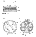
図1(A)〜(C)は、本発明の一実施例としてのブラシレスモータのモータ本体の構成を示す断面図である。このモータ本体100は、外形がそれぞれ略円盤状のステータ部10及びロータ部30を有している。ステータ部10(図1(C))には、回路基板120上に3相を構成する3組の電磁コイル11〜13と、2つの磁気センサ40A,40Bとが設けられている。第1の磁気センサ40Aは1組目のコイル11用のセンサであり、第2の磁気センサ40Bは2組目のコイル12用のセンサである。なお、3組目のコイル13用の磁気センサは実装されていない。以下では、3組の電磁コイル11〜13を「A相コイル11」、「B相コイル12」、「C相コイル13」と呼ぶ。また、磁気センサ40A,40Bを「A相センサ40A」、「B相センサ40B」と呼ぶ。
A. Overview of motor configuration and operation:
1A to 1C are cross-sectional views showing the configuration of a motor body of a brushless motor as an embodiment of the present invention. The motor
ロータ部30(図1(B))には、4つの磁石32が設けられており、ロータ部30の中心軸が回転軸112を構成している。これらの磁石32の磁化方向は図1(B)において紙面と垂直な方向であり、これは図1(A)における上下方向に相当する。
The rotor unit 30 (FIG. 1B) is provided with four
図2(A)〜(D)は、モータの動作時における磁石列とコイル列の位置関係を示す説明図である。図2(A)に示すように、磁石32は一定の磁極ピッチPmで配置されており、隣接する磁石同士が逆方向に磁化されている。また、1つの相のコイル群を構成する2つコイルは、一定のピッチPcで配置されており、常に同じ方向に励磁される。隣接する相のコイル同士は、同相コイル間のピッチPcの1/3だけ離れている。同相コイル間のピッチPcは、磁極ピッチPmの2倍に等しい。磁極ピッチPmは、電気角でπに相当する。なお、電気角の2πは、駆動信号の位相が2πだけ変化したときに移動する機械的な角度又は距離に対応づけられる。本実施例では、駆動信号の位相が2πだけ変化すると、ロータ部30が磁極ピッチPmの2倍だけ移動する。
2A to 2D are explanatory views showing the positional relationship between the magnet array and the coil array during operation of the motor. As shown in FIG. 2A, the
図2(A)は、位相が0又は2πにおける状態を示している。また、図2(B)〜(D)は、位相がπ/2,π,3π/2の時点の状態をそれぞれ示している。なお、図2(A),(C)でA相コイル11のハッチングが省略されているのは、これらのタイミングでA相コイル11の駆動信号の極性が反転する(すなわち励磁方向が反転する)からである。
FIG. 2A shows a state where the phase is 0 or 2π. FIGS. 2B to 2D show the states at the time when the phases are π / 2, π, and 3π / 2, respectively. 2A and 2C, the hatching of the
図3は、モータの正転時のセンサ出力と駆動信号の例を示す説明図である。図3(A)は、A相センサ40Aのセンサ出力SSAと、B相センサ40Bのセンサ出力SSBとを示している。なお、センサ40A,40Bとしては、アナログ出力を有するホールICセンサを利用することができる。図3(B)は、2つのセンサ出力SSA,SSBから合成される模擬的なC相センサ出力SSC(「C相センサ模擬信号SSC」とも呼ぶ)を示している。C相センサ模擬信号SSCの生成方法については後述する。3つのセンサ出力SSA,SSB,SSCは、位相が順次2π/3ずつずれたきれいな3相信号を構成していることが理解できる。
FIG. 3 is an explanatory diagram showing an example of sensor output and drive signals during normal rotation of the motor. FIG. 3A shows the sensor output SSA of the
図3(C)は、これらの3相のセンサ出力SSA,SSB,SSCを利用したPWM制御でそれぞれ生成される3相の駆動信号の例を示している。A相の駆動信号DRVA1,DRVA2は、A相センサ出力SSAと相似形状の実効電圧を有する。なお、A相の第1の駆動信号DRVA1は、センサ出力SSAが正のときにのみパルスを発生する信号であり、第2の駆動信号DRVA2はセンサ出力SSAが正のときにのみパルスを発生する信号であるが、図3(C)ではこれらを合わせて記載している。また、便宜上、第2の駆動信号DRVA2を負側のパルスとして描いている。他の相も同様である。 FIG. 3C shows an example of a three-phase drive signal generated by PWM control using these three-phase sensor outputs SSA, SSB, and SSC. The A-phase drive signals DRVA1 and DRVA2 have effective voltages similar in shape to the A-phase sensor output SSA. The A-phase first drive signal DRVA1 is a signal that generates a pulse only when the sensor output SSA is positive, and the second drive signal DRVA2 generates a pulse only when the sensor output SSA is positive. The signals are shown together in FIG. 3C. For convenience, the second drive signal DRVA2 is drawn as a negative pulse. The same applies to the other phases.
図4は、モータの逆転時のセンサ出力と駆動信号の例を示す説明図である。図3と同様に、逆転時にも、C相センサ出力SSCが他の2相のセンサ出力SSA,SSBから合成され、これらの3つのセンサ出力SSA,SSB,SSCを利用して3相の駆動信号が生成される。 FIG. 4 is an explanatory diagram showing an example of the sensor output and the drive signal when the motor is reversely rotated. Similarly to FIG. 3, during reverse rotation, the C-phase sensor output SSC is synthesized from the other two-phase sensor outputs SSA and SSB, and these three sensor outputs SSA, SSB and SSC are used to drive a three-phase drive signal. Is generated.
B.駆動制御回路の構成:
図5(A)は、本実施例のブラシレスモータの駆動制御回路の構成を示すブロック図である。駆動制御回路200は、CPU220と、C相センサ信号生成部230と、駆動信号生成部240と、3相のドライバ回路250A〜250Cと、AD変換部260を備えている。2つのセンサ出力SSA,SSBは、AD変換部260でデジタル多値信号に変換されて、C相センサ信号生成部230に供給される。C相センサ信号生成部230は、図3(B)に示したC相センサ模擬信号SSCを生成する。C相センサ信号生成部230の内部構成については後述する。駆動信号生成部240は、3相のセンサ出力SSA,SSB,SSCに基づいて、3相の駆動信号(図3(C))を生成する。ドライバ回路250A〜250Cは、これらの3相の駆動信号に従ってモータ本体100内の3相の電磁コイル群11〜13を駆動する。
B. Configuration of drive control circuit:
FIG. 5A is a block diagram showing the configuration of the drive control circuit of the brushless motor of this embodiment. The
図5(B)は、磁気センサ40Aの内部構成の一例を示している。B相用の磁気センサ40Bもこれと同じ構成を有している。この磁気センサ40Aは、ホール素子42と、バイアス調整部44と、ゲイン調整部46とを有している。ホール素子42は、磁束密度Xを測定する。バイアス調整部44はホール素子42の出力Xにバイアス値bを加算し、ゲイン調整部46はゲイン値aを乗ずる。磁気センサ40Aの出力SSA(=Y)は、例えば以下の式(1)又は式(2)で与えられる。
FIG. 5B shows an example of the internal configuration of the
Y=a・X+b …(1)
Y=a(X+b) …(2)
Y = a · X + b (1)
Y = a (X + b) (2)
磁気センサ40Aのゲイン値aとバイアス値bは、CPU220によって磁気センサ40A内に設定される。ゲイン値aとバイアス値bを適切な値に設定することによって、センサ出力SSAを好ましい波形形状に較正することが可能である。B相センサ40Bについても同様である。
The gain value a and the bias value b of the
本実施例では、3相のコイル群のうちの2相(A相とB相)についてのみ磁気センサを実装し、他の1相(C相)については磁気センサを省略している。各磁気センサは、ゲインとバイアス(「オフセット」とも呼ぶ)を適切に設定すれば、好ましい波形形状のセンサ出力を得ることができる。しかしながら、適切な波形形状のセンサ出力をそれぞれ得るためには、それぞれのセンサ出力を実測してゲインとバイアスとを適切な値に設定するための作業(キャリブレーション)が必要になる。本実施例では、3相のうちの2相についてのみ磁気センサを実装しているので、1相分での磁気センサに関するキャリブレーションを省略できるという利点がある。また、実装されている2相の磁気センサの出力SSA,SSBを正しくキャリブレーションすれば、3相の駆動信号の相互の位相を容易に整合させることができるという利点もある。さらに、コストの点からも、センサの数は少ないほど好ましい。 In this embodiment, the magnetic sensor is mounted only for two phases (A phase and B phase) of the three-phase coil group, and the magnetic sensor is omitted for the other one phase (C phase). Each magnetic sensor can obtain a sensor output having a preferable waveform shape by appropriately setting a gain and a bias (also referred to as “offset”). However, in order to obtain sensor outputs having appropriate waveform shapes, it is necessary to perform an operation (calibration) for actually measuring each sensor output and setting the gain and bias to appropriate values. In the present embodiment, since the magnetic sensor is mounted only for two of the three phases, there is an advantage that calibration regarding the magnetic sensor for one phase can be omitted. Further, if the outputs SSA and SSB of the mounted two-phase magnetic sensor are correctly calibrated, there is an advantage that the phases of the three-phase drive signals can be easily matched. Furthermore, from the viewpoint of cost, the smaller the number of sensors, the better.
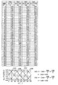
図6は、C相センサ信号生成部230の内部構成を示すブロック図である。C相センサ信号生成部230は、5つのラッチ回路231〜235と、演算回路236とを備えている。第1と第2のラッチ回路231,232は、クロック信号CLKの立ち上がりエッジに同期してA相センサ出力SSAとB相センサ出力SSBとをそれぞれラッチする。第3と第4のラッチ回路233,234は、クロック信号CLKの立ち下がりエッジに同期して、第1と第2のラッチ回路231,232の出力をそれぞれラッチする。演算回路236は、第1と第2のラッチ回路231,232の出力の両方を用いた演算をリアルタイムに実行することによって、C相センサ出力SSCを生成する。第5のラッチ回路235は、演算回路236から出力されたセンサ出力SSCを、クロック信号CLKの立ち下がりエッジに同期してラッチする。この結果、3つのラッチ回路223〜235からは、同じタイミングで3相のセンサ出力SSA,SSB,SSCが出力される。
FIG. 6 is a block diagram illustrating an internal configuration of the C-phase sensor
図6(B)は、演算回路236で実行される演算の内容を示している。この表には、角度θ(位相)に応じた各相のセンサ出力SSA,SSB,SSCの値が示されている。本実施例では、各センサ出力のレンジは、0〜VDD(VDDは電源電圧)の間であるものと仮定している。このとき、C相センサ出力SSCは、以下の演算式に従って演算することができる。
SSC = - (SSB - (VDD/2)) - (SSA - (VDD/2)) + (VDD/2)
= - SSB - SSA + 3/2・(VDD)
FIG. 6B shows the contents of the calculation executed by the
SSC =-(SSB-(VDD / 2))-(SSA-(VDD / 2)) + (VDD / 2)
=-SSB-
なお、演算回路236の代わりに、A相とB相のセンサ出力SSA,SSBを入力値とし、C相センサ出力SSCを出力値とするルックアップテーブルを利用することも可能である。このルックアップテーブルは、上記の演算結果を予め格納しているものであり、演算に基づいてC相センサ出力SSCを得るものである点では演算回路236と同じである。なお、上記の演算を行う回路は、アナログ回路とデジタル回路のいずれでも実現可能である。
Instead of the
図7(A)は、ドライバ回路の内部構成を示している。各相のドライバ回路250A〜250Cは、それぞれH型ブリッジ回路を構成している。例えば、A相のドライバ回路250Aは、駆動信号DRVA1,DRVA2に応じてA相コイル11を駆動する。符号IA1,IA2が付された矢印は、駆動信号DRVA1,DRVA2によって流れる電流方向をそれぞれ示している。他の相も同様である。図7(B)は、3相のコイル群11〜13をスター結線して、トランジスタの数を減らしたドライバ回路250の例を示している。
FIG. 7A shows the internal configuration of the driver circuit. The
図8は、駆動信号生成部240(図5(A))の内部構成と動作を示す説明図である。なお、ここでは図示の便宜上、A相用の回路要素のみを示しているが、B相用とC相用にも同じ回路要素が設けられている。 FIG. 8 is an explanatory diagram showing the internal configuration and operation of the drive signal generator 240 (FIG. 5A). For convenience of illustration, only the circuit elements for the A phase are shown here, but the same circuit elements are provided for the B phase and the C phase.
駆動信号生成部240は、基本クロック生成回路510と、1/N分周器520と、PWM部530と、正逆方向指示値レジスタ540と、乗算器550と、符号化部560と、電圧指令値レジスタ580と、励磁区間設定部590とを備えている。
The drive
基本クロック生成回路510は、所定の周波数を有するクロック信号PCLを発生する回路であり、例えばPLL回路で構成される。分周器520は、このクロック信号PCLの1/Nの周波数を有するクロック信号SDCを発生する。Nの値は所定の一定値に設定される。このNの値は、予めCPU220によって分周器520に設定される。PWM部530は、クロック信号PCL,SDCと、乗算器550から供給される乗算値Maと、正逆方向指示値レジスタ540から供給される正逆方向指示値RIと、符号化部560から供給される正負符号信号Paと、励磁区間設定部590から供給される励磁区間信号Eaとに応じて、A相駆動信号DRVA1,DRVA2(図3(C))を生成する。この動作については後述する。
The basic
正逆方向指示値レジスタ540内には、モータの回転方向を示す値RIがCPU220によって設定される。本実施例では、正逆方向指示値RIがLレベルのときにモータが正転し、Hレベルのときに逆転する。PWM部530に供給される他の信号Ma,Pa,Eaは以下のように決定される。
In the forward / reverse
磁気センサ40Aの出力SSAは、符号化部560に供給される。符号化部560は、センサ出力SSAのレンジを変換するとともに、センサ出力の中位点の値を0に設定する。この結果、符号化部560で生成されるセンサ出力値Xaは、正側の所定の範囲(例えば+127〜0)と負側の所定の範囲(例えば0〜−128)の値を取る。但し、符号化部560から乗算器550に供給されるのは、センサ出力値Xaの絶対値であり、その正負符号は正負符号信号PaとしてPWM部530に供給される。
The output SSA of the
電圧指令値レジスタ580は、CPU220によって設定された電圧指令値Yaを格納する。この電圧指令値Yaは、後述する励磁区間信号Eaとともに、モータの印加電圧を設定する値として機能するものであり、例えば0〜1.0の値を取る。仮に、非励磁区間を設けずに全区間を励磁区間とするように励磁区間信号Eaを設定した場合には、Ya=0は印加電圧をゼロとすることを意味し、Ya=1.0は印加電圧を最大値とすることを意味する。乗算器550は、符号化部560から出力されたセンサ出力値Xaと、電圧指令値Yaとを乗算して整数化し、その乗算値MaをPWM部530に供給する。
Voltage command value register 580 stores voltage command value Ya set by
図8(B)〜8(E)は、乗算値Maが種々の値を取る場合におけるPWM部530の動作を示している。ここでは、全期間が励磁区間であり非励磁区間が無いものと仮定している。PWM部530は、クロック信号SDCの1周期の間に、デューティがMa/Nであるパルスを1つ発生させる回路である。すなわち、図8(B)〜8(E)に示すように、乗算値Maが増加するに従って、A相駆動信号DRVA1,DRVA2のパルスのデューティが増加する。なお、第1の駆動信号DRVA1は、センサ出力SSAが正のときにのみパルスを発生する信号であり、第2の駆動信号DRVA2はセンサ出力SSAが正のときにのみパルスを発生する信号であるが、図8(B)〜8(E)ではこれらを合わせて記載している。また、便宜上、第2の駆動信号DRVA2を負側のパルスとして描いている。
FIGS. 8B to 8E show the operation of the
図9(A)〜9(C)は、センサ出力の波形とPWM部530で生成される駆動信号の波形の対応関係を示す説明図である。図中、「Hiz」は電磁コイルを未励磁状態としたハイインピーダンス状態を意味している。図8で説明したように、A相駆動信号DRVA1,DRVA2はセンサ出力SSAのアナログ波形を利用したPWM制御によって生成される。従って、これらのA相駆動信号DRVA1,DRVA2を用いて、各コイルに、センサ出力SSAの変化と対応するレベル変化を示す実効電圧を供給することが可能である。
FIGS. 9A to 9C are explanatory diagrams illustrating the correspondence relationship between the waveform of the sensor output and the waveform of the drive signal generated by the
PWM部530は、さらに、励磁区間設定部590から供給される励磁区間信号Eaで示される励磁区間のみに駆動信号を出力し、励磁区間以外の区間(非励磁区間)では駆動信号を出力しないように構成されている。図9(C)は、励磁区間信号Eaによって励磁区間EPと非励磁区間NEPを設定した場合の駆動信号波形を示している。励磁区間EPでは図9(B)の駆動信号パルスがそのまま発生し、非励磁区間NEPでは駆動信号パルスが発生しない。このように、励磁区間EPと非励磁区間NEPを設定するようにすれば、センサ出力の中位点近傍(これは逆起電力波形の中位点近傍に相当する)においてコイルを電圧を印加しないので、モータの効率をさらに向上させることが可能である。なお、励磁区間EPは、センサ出力波形(これは逆起電力波形にほぼ等しい)のピークを中心とする対称な区間に設定されることが好ましく、非励磁区間NEPは、センサ出力波形の中位点(中心点)を中心とする対称な区間に設定されることが好ましい。
Further, the
なお、前述したように、電圧指令値Yaを1未満の値に設定すれば、乗算値Maが電圧指令値Yaに比例して小さくなる。従って、電圧指令値Yaによっても、実効的な印加電圧を調整することが可能である。 As described above, when the voltage command value Ya is set to a value less than 1, the multiplication value Ma becomes smaller in proportion to the voltage command value Ya. Therefore, the effective applied voltage can be adjusted also by the voltage command value Ya.
上述の説明から理解できるように、本実施例のモータでは、電圧指令値Yaと、励磁区間信号Eaとの両方を利用して印加電圧を調整することが可能である。望ましい印加電圧と、電圧指令値Ya及び励磁区間信号Eaとの関係は、予め駆動制御回路200(図5(A))内のメモリにテーブルとして格納されていることが望ましい。こうすれば、駆動制御回路200が、外部から望ましい印加電圧の目標値を受信したときに、CPU220がその目標値に応じて、電圧指令値Yaと、励磁区間信号Eaとを駆動信号生成部240に設定することが可能である。なお、印加電圧の調整には、電圧指令値Yaと、励磁区間信号Eaの両方を利用する必要はなく、いずれか一方のみを利用するようにしてもよい。
As can be understood from the above description, in the motor of this embodiment, it is possible to adjust the applied voltage using both the voltage command value Ya and the excitation interval signal Ea. The relationship between the desired applied voltage, the voltage command value Ya, and the excitation interval signal Ea is preferably stored in advance as a table in a memory in the drive control circuit 200 (FIG. 5A). In this way, when the
図10は、PWM部530(図8)の内部構成の一例を示すブロック図である。PWM部530は、カウンタ531と、EXOR回路533と、駆動波形形成部535とを備えている。これらは以下のように動作する。
FIG. 10 is a block diagram showing an example of the internal configuration of the PWM unit 530 (FIG. 8). The
図11は、モータ正転時のPWM部530の動作を示すタイミングチャートである。この図には、2つのクロック信号PCL,SDCと、正逆方向指示値RIと、励磁区間信号Eaと、乗算値Maと、正負符号信号Paと、カウンタ531内のカウント値CM1と、カウンタ531の出力S1と、EXOR回路533の出力S2と、駆動波形形成部535の出力信号DRVA1,DRVA2とが示されている。カウンタ531は、クロック信号SDCの1期間毎に、クロック信号PCLに同期してカウント値CM1を0までダウンカウントする動作を繰り返す。カウント値CM1の初期値は乗算値Maに設定される。なお、図11では、図示の便宜上、乗算値Maとして負の値も描かれているが、カウンタ531で使用されるのはその絶対値|Ma|である。カウンタ531の出力S1は、カウント値CM1が0で無い場合にはHレベルに設定され、カウント値CM1が0になるとLレベルに立ち下がる。
FIG. 11 is a timing chart showing the operation of the
EXOR回路533は、正負符号信号Paと正逆方向指示値RIとの排他的論理和を示す信号S2を出力する。モータが正転する場合には、正逆方向指示値RIがLレベルである。従って、EXOR回路533の出力S2は、正負符号信号Paと同じ信号となる。駆動波形形成部535は、カウンタ531の出力S1と、EXOR回路533の出力S2から、駆動信号DRVA1,DRVA2を生成する。すなわち、カウンタ531の出力S1のうち、EXOR回路533の出力S2がLレベルの期間の信号を第1の駆動信号DRVA1として出力し、出力S2がHレベルの期間の信号を第2の駆動信号DRVA2として出力する。なお、図11の右端部付近では、励磁区間信号EaがLレベルに立ち下がり、これによって非励磁区間NEPが設定されている。従って、この非励磁区間NEPでは、いずれの駆動信号DRVA1,DRVA2も出力されず、ハイインピーダンス状態に維持される。
The
図12は、モータ逆転時のPWM部530の動作を示すタイミングチャートである。モータ逆転時には、正逆方向指示値RIがHレベルに設定される。この結果、2つの駆動信号DRVA1,DRVA2が図11から入れ替わっており、この結果、モータが逆転することが理解できる。
FIG. 12 is a timing chart showing the operation of the
図13は、励磁区間設定部590の内部構成と動作を示す説明図である。励磁区間設定部590は、電子可変抵抗器592と、電圧比較器594,596と、OR回路598とを有している。電子可変抵抗器592の抵抗値Rvは、CPU220によって設定される。電子可変抵抗器592の両端の電圧V1,V2は、電圧比較器594,596の一方の入力端子に与えられている。電圧比較器594,596の他方の入力端子には、センサ出力SSAが供給されている。電圧比較器594,596の出力信号Sp,Snは、OR回路598に入力されている。OR回路598の出力は、励磁区間と非励磁区間とを区別するための励磁区間信号Eaである。
FIG. 13 is an explanatory diagram showing the internal configuration and operation of the excitation
図13(B)は、励磁区間設定部590の動作を示している。電子可変抵抗器592の両端電圧V1,V2は、抵抗値Rvを調整することによって変更される。具体的には、両端電圧V1,V2は、電圧レンジの中央値(=VDD/2)からの差分が等しい値に設定される。センサ出力SSAが第1の電圧V1よりも高い場合には第1の電圧比較器594の出力SpがHレベルとなり、一方、センサ出力SSAが第2の電圧V2よりも低い場合には第2の電圧比較器596の出力SnがHレベルとなる。励磁区間信号Eaは、これらの出力信号Sp,Snの論理和を取った信号である。従って、図13(B)の下部に示すように、励磁区間信号Eaは、励磁区間EPと非励磁区間NEPとを示す信号として使用することができる。励磁区間EPと非励磁区間NEPの設定は、CPU220が可変抵抗値Rvを調整することによって行なわれる。
FIG. 13B shows the operation of the excitation
以上のように、第1実施例のブラシレスモータでは、3相のコイル群のうちの2相についてのみ磁気センサを実装し、他の1相については磁気センサを省略しているので、センサのキャリブレーションに関する作業負担を軽減することができ、また、3相の駆動信号の位相を容易に整合させることができる。さらに、低コストで効率の良いモータを提供することができる。 As described above, in the brushless motor of the first embodiment, the magnetic sensor is mounted only for two phases of the three-phase coil group and the magnetic sensor is omitted for the other one phase. The work load related to the operation can be reduced, and the phases of the three-phase drive signals can be easily matched. Furthermore, a low-cost and efficient motor can be provided.
C.他の実施例:
図14は、本発明の他の実施例としてのブラシレスモータのモータ本体の構成を示す断面図である。このモータ本体100aのステータ部10及びロータ部30は、外形がそれぞれ略円筒状に形成されており、ステータ部10の外周をロータ部30が周回する。
C. Other examples:
FIG. 14 is a cross-sectional view showing a configuration of a motor body of a brushless motor as another embodiment of the present invention. The
この例からも理解できるように、本発明のブラシレスモータの機械的形状は、種々の形状を採用することが可能である。また、本発明は、3相4極モータに限らず、任意の相数及び極数のブラシレスモータに適用可能である。 As can be understood from this example, various shapes can be adopted as the mechanical shape of the brushless motor of the present invention. The present invention is not limited to a three-phase four-pole motor, and can be applied to a brushless motor having any number of phases and poles.
図15は、本発明の更に他の実施例としての4相ブラシレスモータにおける模擬的センサ出力の演算方法を示している。なお、4相ブラシレスモータの機械的構造は省略する。4相ブラシレスモータでは、C相センサ出力SSCとD相センサ出力SSDとが、以下の演算式に従って演算される。
SSC = - (SSA - (VDD/2)) + (VDD/2)
= - SSA + VDD
SSD = - (SSB - (VDD/2)) + (VDD/2)
= - SSB + VDD
FIG. 15 shows a method for calculating a simulated sensor output in a four-phase brushless motor as still another embodiment of the present invention. Note that the mechanical structure of the four-phase brushless motor is omitted. In the four-phase brushless motor, the C-phase sensor output SSC and the D-phase sensor output SSD are calculated according to the following arithmetic expression.
SSC =-(SSA-(VDD / 2)) + (VDD / 2)
=-SSA + VDD
SSD =-(SSB-(VDD / 2)) + (VDD / 2)
=-SSB + VDD
なお、通常は、m相(mは3以上の整数)の電磁コイル群のためのm個の磁気センサ出力の相互関係は、何らかの関数(三角関数など)によって表わされる。従って、m相のうちのn個(nは2以上m未満の整数)の相のみに磁気センサを実装するようにしても、磁気センサが実装されていない(m−n)相の模擬センサ出力を、n相の磁気センサの出力を変数とした演算によって求めることが可能である。なお、(m−n)相の模擬センサ出力は、n個のセンサ出力のうちの1つ以上を用いてそれぞれ生成することが好ましく、2つ以上を用いて生成することがさらに好ましい。例えば、上記第1実施例のような3相モータの場合には、2相のセンサ出力のうちの一方だけでは残りの相のセンサ出力が一意に決まらず、2つのセンサ出力の両方を用いて初めて残りの相のセンサ出力を決定することが可能である。 In general, the correlation between m magnetic sensor outputs for an m-phase (m is an integer of 3 or more) electromagnetic coil group is expressed by some function (such as a trigonometric function). Therefore, even if the magnetic sensor is mounted only on n (n is an integer less than or equal to 2 and less than m) of the m phases, the simulated sensor output of the (mn) phase where the magnetic sensor is not mounted. Can be obtained by calculation using the output of the n-phase magnetic sensor as a variable. The simulated sensor output of the (mn) phase is preferably generated using one or more of n sensor outputs, and more preferably generated using two or more. For example, in the case of a three-phase motor as in the first embodiment, the sensor output of the remaining phase is not uniquely determined by only one of the two-phase sensor outputs, and both of the two sensor outputs are used. It is possible for the first time to determine the sensor output of the remaining phase.
このように、本発明は、m相(mは3以上の整数)の電磁コイル群のうちのn相(nは2以上m未満の整数)の電磁コイル群に対応してn個の磁気センサを実装し、これらのn相の磁気センサの出力からm相のコイル群の駆動信号を生成するものに適用可能である。また、本発明は、実装されていない(m−n)相の電磁コイル群のための(m−n)組の駆動信号を、実装されているn個の磁気センサのセンサ出力のうちの1つ以上をそれぞれ用いて生成するものに適用可能である。 Thus, the present invention provides n magnetic sensors corresponding to the n-phase (n is an integer of 2 or more and less than m) of the m-phase (m is an integer of 3 or more) electromagnetic coil groups. Can be applied, and the drive signal of the m-phase coil group can be generated from the output of these n-phase magnetic sensors. In addition, the present invention provides (mn) sets of drive signals for an unmounted (mn) phase electromagnetic coil group as one of the sensor outputs of n mounted magnetic sensors. It is applicable to what is generated using two or more.
D.変形例:
なお、この発明は上記の実施例や実施形態に限られるものではなく、その要旨を逸脱しない範囲において種々の態様において実施することが可能であり、例えば次のような変形も可能である。
D. Variations:
The present invention is not limited to the above-described examples and embodiments, and can be implemented in various modes without departing from the gist thereof. For example, the following modifications are possible.
D1.変形例1:
上記実施例ではアナログ磁気センサを利用していたが、アナログ磁気センサの代わりに、多値のアナログ的出力を有するデジタル磁気センサを使用してもよい。アナログ磁気センサも多値出力を有するデジタル磁気センサも、アナログ的変化を示す出力信号を有する点で共通している。なお、本明細書において、「アナログ的変化を示す出力信号」とは、オン/オフの2値出力ではなく、3値以上の多数レベルを有するデジタル出力信号と、アナログ出力信号との両方を包含する広い意味で使用されている。
D1. Modification 1:
In the above embodiment, an analog magnetic sensor is used, but a digital magnetic sensor having a multi-valued analog output may be used instead of the analog magnetic sensor. An analog magnetic sensor and a digital magnetic sensor having a multi-value output are common in that they have an output signal indicating an analog change. In this specification, “an output signal indicating an analog change” includes both a digital output signal having multiple levels of three or more and an analog output signal, not an on / off binary output. Used in a broad sense.
D2.変形例2:
PWM回路としては、図8に示した回路以外の種々の回路構成を採用することが可能である。例えば、センサ出力と基準三角波とを比較することによってPWM制御を行う回路を利用してもよい。また、PWM制御以外の方法で駆動信号を生成するようにしてもよい。また、PWM制御以外の方法で駆動信号を生成する回路を採用してもよい。例えば、センサ出力を増幅してアナログ駆動信号を生成する回路を採用することも可能である。
D2. Modification 2:
As the PWM circuit, various circuit configurations other than the circuit shown in FIG. 8 can be adopted. For example, a circuit that performs PWM control by comparing the sensor output with a reference triangular wave may be used. Further, the drive signal may be generated by a method other than PWM control. A circuit that generates a drive signal by a method other than PWM control may be employed. For example, it is possible to employ a circuit that amplifies the sensor output and generates an analog drive signal.
D3.変形例3:
上記実施例では、磁気センサが実装されていない相に関する模擬センサ出力を生成し、これを用いてその相の駆動信号を生成していたが、これ以外の方法で磁気センサが実装されていない相の駆動信号を生成するようにしてもよい。例えば、磁気センサが実装されているn相の駆動信号を生成し、これらのn相の駆動信号を用いて、磁気センサが実装されていない(m−n)相の駆動信号を生成するようにしてもよい。
D3. Modification 3:
In the above embodiment, a simulated sensor output related to a phase where the magnetic sensor is not mounted is generated, and a drive signal of the phase is generated using this, but the phase where the magnetic sensor is not mounted by any other method. The drive signal may be generated. For example, an n-phase drive signal in which the magnetic sensor is mounted is generated, and an (mn) -phase drive signal in which the magnetic sensor is not mounted is generated using these n-phase drive signals. May be.
D4.変形例4:
本発明は、ファンモータ、時計(針駆動)、ドラム式洗濯機(単一回転)、ジェットコースタ、振動モータなどの種々の装置のモータに適用可能である。
D4. Modification 4:
The present invention can be applied to motors of various devices such as a fan motor, a timepiece (hand drive), a drum-type washing machine (single rotation), a roller coaster, and a vibration motor.
10…ステータ部
11〜13…電磁コイル
30…ロータ部
32…磁石
40A,40B…磁気センサ
42…ホール素子
44…バイアス調整部
46…ゲイン調整部
100…モータ本体
112…回転軸
120…回路基板
200…駆動制御回路
220…CPU
221〜235…ラッチ回路
230…C相センサ信号生成部
236…演算回路
240…駆動信号生成部
250…ドライバ回路
260…AD変換部
510…基本クロック生成回路
520…分周器
530…PWM部
531…カウンタ
533…EXOR回路
535…駆動波形形成部
540…正逆方向指示値レジスタ
550…乗算器
560…符号化部
580…指令値レジスタ
590…励磁区間設定部
592…電子可変抵抗器
594,596…電圧比較器
598…OR回路
DESCRIPTION OF
221 to 235...
Claims (4)
3相の電磁コイル群を有するコイル列と、
複数の永久磁石を有する磁石列と、
前記3相の電磁コイル群のうちの2相の電磁コイル群に対応付けられた2個の磁気センサであって、前記磁石列と前記コイル列の相対位置を検出するための2個の磁気センサと、
前記2個の磁気センサのセンサ出力を利用して、前記コイル列を駆動する駆動制御回路と、
を備え、
前記駆動制御回路は、
前記2個の磁気センサに対応付けられていない1相の電磁コイル群のための1個の模擬的なセンサ出力を、前記2個の磁気センサのセンサ出力を変数として用いた以下の演算式で表された演算に基づいて生成する模擬センサ出力生成部と、
前記2個の磁気センサのセンサ出力と前記1個の模擬的なセンサ出力とを含む3個のセンサ出力に応じて、前記3相の電磁コイル群のための3組の駆動信号を生成する駆動信号生成部と、
を備え、
各前記2個の磁気センサは、各前記2個の磁気センサのセンサ出力のゲインとオフセットであるバイアスとを個別に調整してそれぞれ正弦波形状のセンサ出力を得るためのゲイン及びバイアス調整部を有し、
前記駆動信号生成部は、設定される正逆方向指示値が正転を示す場合には、正転に対応する前記3個のセンサ出力に応じて正転に対応する前記3組の駆動信号を生成し、前記正逆方向指示値が逆転を示す場合には、逆転に対応する前記3個のセンサ出力に応じて逆転に対応する前記3組の駆動信号を生成する、ブラシレスモータ。
SSC=−SSB−SSA+3/2・(VDD)
ここで、SSA,SSBは前記2個のセンサ出力であり、SSCは前記1個の模擬的なセンサ出力であり、VDDは前記2個の磁気センサの電源電圧である。 A brushless motor,
A coil array having a three-phase electromagnetic coil group;
A magnet array having a plurality of permanent magnets;
A two magnetic sensors associated with the two-phase electromagnetic coil group of one of the electromagnetic coil group of the three-phase, two magnetic sensors for detecting the relative position of the coil array and the magnet array When,
A drive control circuit for driving the coil array using sensor outputs of the two magnetic sensors;
With
The drive control circuit includes:
One simulated sensor output for a one-phase electromagnetic coil group not associated with the two magnetic sensors is expressed by the following arithmetic expression using the sensor outputs of the two magnetic sensors as variables. A simulated sensor output generator for generating based on the represented calculation;
Depending on the three sensor outputs including said one simulated sensor output and the sensor output of the two magnetic sensors, driving to generate three sets of driving signals for the electromagnetic coil group of the 3-phase A signal generator;
With
Each said two magnetic sensors, the gain and bias adjustment unit for obtaining a sensor output of each of the two sensor outputs of the magnetic sensor gain and each sine wave shape and a bias adjust individually the offset Have
When the set forward / reverse direction instruction value indicates normal rotation, the drive signal generation unit outputs the three sets of drive signals corresponding to normal rotation according to the three sensor outputs corresponding to normal rotation. generated, wherein when the forward and reverse direction value indicates reverse rotation, generates the three sets of drive signals corresponding to the reverse rotation in response to the three sensor output corresponding to the reverse rotation, the brushless motor.
SSC = -SSB-SSA + 3/2. (VDD)
Here, SSA and SSB are the two sensor outputs, SSC is the one simulated sensor output, and VDD is a power supply voltage of the two magnetic sensors.
前記模擬センサ出力生成部は、前記2個の磁気センサのセンサ出力を用いたリアルタイム演算によって前記模擬的なセンサ出力を生成する、ブラシレスモータ。 The brushless motor according to claim 1,
The simulated sensor output generation unit is a brushless motor that generates the simulated sensor output by real-time calculation using sensor outputs of the two magnetic sensors.
前記模擬センサ出力生成部は、前記2個の磁気センサのセンサ出力を入力値とし前記模擬的なセンサ出力を出力値とするルックアップテーブルを用いて前記模擬的なセンサ出力を生成する、ブラシレスモータ。 The brushless motor according to claim 1,
The simulated sensor output generation unit generates the simulated sensor output using a look-up table having the sensor outputs of the two magnetic sensors as input values and the simulated sensor output as output values. .
前記磁気センサは、前記磁石列と前記コイル列の相対位置に応じてアナログ的変化を示す出力信号を出力するセンサである、ブラシレスモータ。 The brushless motor according to any one of claims 1 to 3 ,
The magnetic sensor is a brushless motor that outputs an output signal indicating an analog change according to a relative position between the magnet array and the coil array.
Priority Applications (3)
| Application Number | Priority Date | Filing Date | Title |
|---|---|---|---|
| JP2006230779A JP4904996B2 (en) | 2006-08-28 | 2006-08-28 | Brushless motor |
| US11/895,487 US7733040B2 (en) | 2006-08-28 | 2007-08-24 | Brushless motor |
| CN2007101477037A CN101136575B (en) | 2006-08-28 | 2007-08-24 | Brushless motor |
Applications Claiming Priority (1)
| Application Number | Priority Date | Filing Date | Title |
|---|---|---|---|
| JP2006230779A JP4904996B2 (en) | 2006-08-28 | 2006-08-28 | Brushless motor |
Publications (3)
| Publication Number | Publication Date |
|---|---|
| JP2008054474A JP2008054474A (en) | 2008-03-06 |
| JP2008054474A5 JP2008054474A5 (en) | 2008-12-04 |
| JP4904996B2 true JP4904996B2 (en) | 2012-03-28 |
Family
ID=39112735
Family Applications (1)
| Application Number | Title | Priority Date | Filing Date |
|---|---|---|---|
| JP2006230779A Expired - Fee Related JP4904996B2 (en) | 2006-08-28 | 2006-08-28 | Brushless motor |
Country Status (3)
| Country | Link |
|---|---|
| US (1) | US7733040B2 (en) |
| JP (1) | JP4904996B2 (en) |
| CN (1) | CN101136575B (en) |
Families Citing this family (6)
| Publication number | Priority date | Publication date | Assignee | Title |
|---|---|---|---|---|
| US7795827B2 (en) * | 2008-03-03 | 2010-09-14 | Young-Chun Jeung | Control system for controlling motors for heating, ventilation and air conditioning or pump |
| CN102011744A (en) * | 2009-09-07 | 2011-04-13 | 鸿富锦精密工业(深圳)有限公司 | Multi-fan control system |
| GB2515086B (en) * | 2013-06-13 | 2015-10-07 | Dyson Technology Ltd | Method of controlling of a brushless permanent-magnet motor |
| GB201310575D0 (en) | 2013-06-13 | 2013-07-31 | Dyson Technology Ltd | Method of controllinf of a brushless permanent-magnet motor |
| US9431938B2 (en) | 2013-06-13 | 2016-08-30 | Dyson Technology Limited | Method of controlling a brushless permanent-magnet motor |
| US11074378B1 (en) * | 2020-05-07 | 2021-07-27 | Jsol Corporation | Non-transitory computer readable recording medium storing a computer program, simulation method and simulation device for simulating dynamic behavior of electromagnetic component |
Family Cites Families (16)
| Publication number | Priority date | Publication date | Assignee | Title |
|---|---|---|---|---|
| JPS6096191A (en) * | 1983-10-27 | 1985-05-29 | Sankyo Seiki Mfg Co Ltd | Drive circuit of brushless motor |
| JPH02214496A (en) * | 1989-02-14 | 1990-08-27 | Fanuc Ltd | Ac motor controlling system |
| US5157311A (en) * | 1990-07-31 | 1992-10-20 | Matsushita Electric Industrial Co., Ltd. | Brushless motor |
| US5864192A (en) * | 1992-07-09 | 1999-01-26 | Seiko Epson Corporation | Brushless motor with magnetic sensor to detect leaked magnetic flux |
| US5352962A (en) * | 1993-04-19 | 1994-10-04 | Sug Lithography Systems, Inc. | Brushless polyphase reduced force variation motor |
| JPH08237986A (en) * | 1995-02-27 | 1996-09-13 | Hitachi Ltd | Rotational position detector and detecting method |
| JPH1075594A (en) | 1996-08-29 | 1998-03-17 | Sankyo Seiki Mfg Co Ltd | Drive controller for brushless motor |
| JP4619483B2 (en) | 2000-04-17 | 2011-01-26 | パナソニック株式会社 | Electric device |
| JP2001327186A (en) * | 2000-05-12 | 2001-11-22 | Matsushita Electric Ind Co Ltd | Current detecting device for three-phase synchronous motor |
| JP4131510B2 (en) * | 2000-11-15 | 2008-08-13 | 松下電器産業株式会社 | Resistance value selection method for brushless motor device |
| JP4307004B2 (en) * | 2002-03-11 | 2009-08-05 | キヤノン株式会社 | Image forming apparatus and DC motor drive control circuit |
| DE602004030010D1 (en) * | 2004-05-18 | 2010-12-23 | Seiko Epson Corp | Motor |
| JP4478537B2 (en) * | 2004-09-03 | 2010-06-09 | 日本ビクター株式会社 | Brushless motor |
| GB0422201D0 (en) * | 2004-10-07 | 2004-11-03 | Trw Ltd | Motor drive control |
| JP4022552B2 (en) * | 2005-05-18 | 2007-12-19 | 三菱電機株式会社 | Brushless motor drive method and drive control apparatus thereof |
| JP4178523B2 (en) * | 2006-02-15 | 2008-11-12 | セイコーエプソン株式会社 | Motor and motor drive system |
-
2006
- 2006-08-28 JP JP2006230779A patent/JP4904996B2/en not_active Expired - Fee Related
-
2007
- 2007-08-24 US US11/895,487 patent/US7733040B2/en not_active Expired - Fee Related
- 2007-08-24 CN CN2007101477037A patent/CN101136575B/en not_active Expired - Fee Related
Also Published As
| Publication number | Publication date |
|---|---|
| US20080048593A1 (en) | 2008-02-28 |
| JP2008054474A (en) | 2008-03-06 |
| CN101136575A (en) | 2008-03-05 |
| CN101136575B (en) | 2011-09-21 |
| US7733040B2 (en) | 2010-06-08 |
Similar Documents
| Publication | Publication Date | Title |
|---|---|---|
| US8917041B2 (en) | Phase-shift detection device, motor drive device, brushless motor, and phase-shift detection method | |
| JP2012090467A (en) | Linear motor | |
| US7880319B2 (en) | Power generating device utilizing hydrodynamic force | |
| KR100905357B1 (en) | Drive circuit of motor, small electric motor, actuator | |
| JP4618201B2 (en) | Electric motor | |
| KR101061665B1 (en) | Driver circuit | |
| JP4720856B2 (en) | Single phase brushless motor | |
| JP4904996B2 (en) | Brushless motor | |
| JP5541332B2 (en) | Robot and moving body | |
| JP2008092789A (en) | Brushless generator | |
| JP4506730B2 (en) | Electric motor | |
| US8089231B2 (en) | Electric motor, method for correcting sensor output for the same, and control circuit | |
| JP2022062707A (en) | Magnetic sensor system for motor control | |
| JP5151487B2 (en) | Brushless motor | |
| JP4998070B2 (en) | Brushless motor | |
| JP5168988B2 (en) | Brushless motor and control method thereof | |
| JP2008061526A (en) | Frost-protective fan system | |
| JP5162957B2 (en) | Method for correcting sensor output of electric motor and electric motor | |
| JP5040444B2 (en) | PWM control circuit and motor | |
| JP2012065505A (en) | Electric motor | |
| JP2010045908A (en) | Motor | |
| JP2010045907A (en) | Apparatus and method for creating induced voltage wave table | |
| KR100583452B1 (en) | Signal generator for controlling rotor location of Brushless DC motor | |
| JP2002369571A (en) | Brushless motor | |
| JP2012152015A (en) | Electromechanical device and robot |
Legal Events
| Date | Code | Title | Description |
|---|---|---|---|
| A521 | Written amendment |
Free format text: JAPANESE INTERMEDIATE CODE: A523 Effective date: 20081016 |
|
| A621 | Written request for application examination |
Free format text: JAPANESE INTERMEDIATE CODE: A621 Effective date: 20081016 |
|
| A977 | Report on retrieval |
Free format text: JAPANESE INTERMEDIATE CODE: A971007 Effective date: 20110126 |
|
| A131 | Notification of reasons for refusal |
Free format text: JAPANESE INTERMEDIATE CODE: A131 Effective date: 20110201 |
|
| A521 | Written amendment |
Free format text: JAPANESE INTERMEDIATE CODE: A523 Effective date: 20110314 |
|
| A131 | Notification of reasons for refusal |
Free format text: JAPANESE INTERMEDIATE CODE: A131 Effective date: 20110412 |
|
| A521 | Written amendment |
Free format text: JAPANESE INTERMEDIATE CODE: A523 Effective date: 20110602 |
|
| A131 | Notification of reasons for refusal |
Free format text: JAPANESE INTERMEDIATE CODE: A131 Effective date: 20110621 |
|
| A521 | Written amendment |
Free format text: JAPANESE INTERMEDIATE CODE: A523 Effective date: 20110728 |
|
| TRDD | Decision of grant or rejection written | ||
| A01 | Written decision to grant a patent or to grant a registration (utility model) |
Free format text: JAPANESE INTERMEDIATE CODE: A01 Effective date: 20111213 |
|
| A01 | Written decision to grant a patent or to grant a registration (utility model) |
Free format text: JAPANESE INTERMEDIATE CODE: A01 |
|
| A61 | First payment of annual fees (during grant procedure) |
Free format text: JAPANESE INTERMEDIATE CODE: A61 Effective date: 20111226 |
|
| FPAY | Renewal fee payment (event date is renewal date of database) |
Free format text: PAYMENT UNTIL: 20150120 Year of fee payment: 3 |
|
| R150 | Certificate of patent or registration of utility model |
Free format text: JAPANESE INTERMEDIATE CODE: R150 |
|
| S531 | Written request for registration of change of domicile |
Free format text: JAPANESE INTERMEDIATE CODE: R313531 |
|
| R350 | Written notification of registration of transfer |
Free format text: JAPANESE INTERMEDIATE CODE: R350 |
|
| S111 | Request for change of ownership or part of ownership |
Free format text: JAPANESE INTERMEDIATE CODE: R313113 |
|
| R350 | Written notification of registration of transfer |
Free format text: JAPANESE INTERMEDIATE CODE: R350 |
|
| S131 | Request for trust registration of transfer of right |
Free format text: JAPANESE INTERMEDIATE CODE: R313135 |
|
| SZ02 | Written request for trust registration |
Free format text: JAPANESE INTERMEDIATE CODE: R313Z02 |
|
| S131 | Request for trust registration of transfer of right |
Free format text: JAPANESE INTERMEDIATE CODE: R313135 |
|
| SZ02 | Written request for trust registration |
Free format text: JAPANESE INTERMEDIATE CODE: R313Z02 |
|
| R250 | Receipt of annual fees |
Free format text: JAPANESE INTERMEDIATE CODE: R250 |
|
| R350 | Written notification of registration of transfer |
Free format text: JAPANESE INTERMEDIATE CODE: R350 |
|
| LAPS | Cancellation because of no payment of annual fees |