JP4898351B2 - Switching power supply - Google Patents
Switching power supply Download PDFInfo
- Publication number
- JP4898351B2 JP4898351B2 JP2006231975A JP2006231975A JP4898351B2 JP 4898351 B2 JP4898351 B2 JP 4898351B2 JP 2006231975 A JP2006231975 A JP 2006231975A JP 2006231975 A JP2006231975 A JP 2006231975A JP 4898351 B2 JP4898351 B2 JP 4898351B2
- Authority
- JP
- Japan
- Prior art keywords
- output
- voltage
- power supply
- load
- switching power
- Prior art date
- Legal status (The legal status is an assumption and is not a legal conclusion. Google has not performed a legal analysis and makes no representation as to the accuracy of the status listed.)
- Expired - Fee Related
Links
Images


Description
本発明は、1つのトランスの二次側から少なくとも第1の出力および第2の出力を供給し、第1の出力からトランスの一次側にフィードバック制御を行い出力電圧を制御するスイッチング電源装置に関し、特にその第2の出力の電圧変動の低減に関するものである。 The present invention relates to a switching power supply device that supplies at least a first output and a second output from a secondary side of one transformer, and performs feedback control from the first output to the primary side of the transformer to control an output voltage. In particular, it relates to the reduction of the voltage fluctuation of the second output.
スイッチング電源には、1つのトランスからの複数出力のうち1出力の電圧をフィードバックして出力電圧を制御し、かつ複数の負荷に電力を供給する種類の装置がある。このようなスイッチング電源装置には、出力の電流負荷によって他の出力電圧が変動するクロスレギュレーション特性を有するものがある。 There is a type of switching power supply in which a voltage of one output among a plurality of outputs from one transformer is fed back to control an output voltage and power is supplied to a plurality of loads. Some of these switching power supply devices have cross regulation characteristics in which other output voltages vary depending on the output current load.
このようなスイッチング電源装置では、例えば特許文献1のように、フィードバック対象の出力電圧の精度が良い出力に、負荷の大きさが制御可能なダミー負荷を接続する。そして、スイッチング電源装置が接続されている負荷の駆動指令に合わせて、制御部によってダミー負荷の大きさを制御し、フィードバック対象外の出力電圧の低下を防止することを行っているものがある。
In such a switching power supply device, as in
また、特許文献2のように、フィードバック対象ではない出力に出力電圧を安定化するためにダミー負荷を接続する。そして、その出力電圧を低下させるタイミングでダミー負荷に流れる電流を制御するように電源外部信号で制御し、ダミー負荷での不要な損失を低減し、出力電圧の変動範囲を小さくするようにしたものがある。
前述の特許文献1に示す従来例では、フィードバック対象外の出力負荷が大きくなり出力電圧が低下した時に、フィードバック対象の出力に接続したダミー負荷の電流を増加させてフィードバック対象外の出力電圧を上昇させている。しかし、フィードバック対象外の出力の負荷が小さい時の出力電圧上昇に対しては、その出力にダミー抵抗を接続していないため、出力電圧を適切に低減する制御を行うことができないという問題がある。
In the conventional example shown in the above-mentioned
また、前述の特許文献2に示す従来例では、フィードバック対象外の出力の電圧上昇を防止するためにダミー抵抗をフィードバック対象外の出力に接続している。そして、電圧上昇の好ましくない時にはフィードバック対象外の出力の電圧上昇をダミー抵抗に通電することで低減している。しかし、フィードバック対象外の出力の負荷電流の増大によって電圧下降が発生した場合には、逆に電圧を上昇させることができなないという問題がある。 Further, in the conventional example shown in Patent Document 2 described above, a dummy resistor is connected to an output that is not a feedback target in order to prevent a voltage increase of the output that is not a feedback target. When the voltage rise is not desirable, the voltage rise of the output not subject to feedback is reduced by energizing the dummy resistor. However, when a voltage drop occurs due to an increase in the load current of an output that is not a feedback target, there is a problem that the voltage cannot be raised.
本発明は、このような状況のもとでなされたもので、複数出力を有するスイッチング電源装置において、同一のダミー抵抗を用いて出力の電圧上昇制限と電圧低下制限を実現することを課題とするものである。 The present invention has been made under such circumstances, and it is an object of the present invention to realize output voltage increase limitation and voltage decrease limitation using the same dummy resistor in a switching power supply device having a plurality of outputs. Is.
前記課題を解決するため、本発明では、スイッチング電源装置を次の(1)のとおりに構成する。 In order to solve the above problems, in the present invention, the switching power supply device is configured as described in (1 ) below.
(1)トランスの二次側から第1の出力を第1の負荷に供給する第1出力手段と、前記トランスの二次側から第2の出力を第2の負荷に供給する第2出力手段と、を備え、前記第1の出力を前記トランスの一次側にフィードバックして、フィードバックした出力に応じて前記第1の出力を制御するスイッチング電源装置において、前記第2の出力が第1所定値以上になった場合に、前記第2の出力をダミー負荷を介して前記第1出力手段に流すことにより前記第2の出力の電圧上昇を制限する電圧上昇制限手段と、前記第2の出力が前記第1所定値より小さい第2所定値以下になった場合に、前記第1の出力を前記ダミー負荷に流すことにより前記第2の出力電圧の低下を制限する電圧低下制限手段と、を備えたことを特徴とするスイッチング電源装置。 (1) a first output means for supplying the secondary side or we first output transformer to the first load, the second supplying a second output from the secondary side of the transformer to the second load and an output unit, by feeding back the first output to the primary side of the transformer, the switching power supply for controlling said first output according to the output of the feedback, the second output is the if it becomes more than a plant value, the voltage rise limiting means for limiting the voltage rise of the second output by flowing the second output to the first output means via the dummy load, the second of when the output is below the first plant value smaller than the first plant value, the first and the second output voltage by flowing an output to the dummy load voltage drop limiting means for limiting the decrease in the switching, characterized in that it comprises a and Power supply.
本発明によれば、同一のダミー抵抗を用いて出力の電圧上昇制限と電圧低下制限を実現することができる。これにより、電圧上昇制限および電圧低下制限にそれぞれ対応した個別のダミー抵抗を設置する必要がなく、安価な構成で容易に電圧上昇制限および電圧低下制限を実現することができる。 According to the present invention, it is possible to realize output voltage rise restriction and voltage drop restriction using the same dummy resistor. Thereby, it is not necessary to install individual dummy resistors respectively corresponding to the voltage rise restriction and the voltage drop restriction, and the voltage rise restriction and the voltage drop restriction can be easily realized with an inexpensive configuration.
また、出力に対応する負荷が無いなど、出力電圧の低減が不要な状態で、無駄な電力消費を防止し、低消費電力化が可能となる。 In addition, wasteful power consumption can be prevented and power consumption can be reduced when there is no need to reduce the output voltage, for example, there is no load corresponding to the output.
以下本発明を実施するための最良の形態を、実施例により詳しく説明する。 Hereinafter, the best mode for carrying out the present invention will be described in detail with reference to examples.
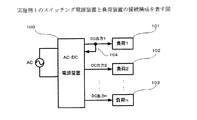
図1は、実施例1である“スイッチング電源装置”と負荷装置の接続関係を表す図である。
100はスイッチング電源装置全体を表したブロックであり、商用電源等の交流(AC)供給源からスイッチング電源装置100内で直流(DC)に変換するスイッチング電源である。ACからDCへの変換は後述する整流回路とスイッチング方式にて行うものとする。
101はスイッチング電源装置100に接続された負荷1を表しており、DC出力1がスイッチング電源装置100から供給されるように接続されている。また、DC出力1は所定の出力電圧となるように電圧変動を抑え、負荷の電流による電圧変動も抑えるため、その出力をフィードバックする経路104を有するものである。
FIG. 1 is a diagram illustrating a connection relationship between a “switching power supply device” according to the first embodiment and a load device.
102はスイッチング電源装置100に接続された別の負荷2を表しており、DC出力2がスイッチング電源装置100から供給されるように接続されている。本実施例では、負荷2へのDC出力2はフィードバックする経路が無い構成である。
103はスイッチング電源装置100に接続されたn番目の負荷nを表している。
このように、スイッチング電源装置100は、複数の出力を有し、そのうち一つの出力をフィードバックすることでその出力を安定させる構成であり、その他の出力は電圧をフィードバックしていない構成の電源装置であることを表している。
As described above, the switching
図2は、本実施例のスイッチング電源装置の構成とダミー負荷を表す図である。
200はスイッチング電源装置100内の整流ダイオードであり、AC供給源からの交流電圧を直流電圧に変換するダイオードブリッジである。整流された電圧は一次平滑コンデンサ201にて平滑される。
202はスイッチング電源装置100内にてスイッチング素子203を制御する電源制御ICである。本実施例では、フライバック型のスイッチング電源にて説明する。
204はスイッチング電源用のトランスであり、一次側と二次側を絶縁してDC出力1およびDC出力2を生成している。一次側は、一次主巻線204a、電源供給用巻線204bから構成される。二次側は、二次側出力1巻線204c、二次側出力2巻線204dで構成される。
FIG. 2 is a diagram illustrating a configuration and a dummy load of the switching power supply device according to the present embodiment.
A
A
205は二次側出力1巻線204cに接続されている整流ダイオードであり、一次主巻線204aの巻数と二次側出力1巻線204cの巻数に対応したAC出力1を半波整流し、整流出力は二次側平滑コンデンサ206にて平滑する。
207は二次側出力2巻線204dに接続されている整流ダイオードであり、一次主巻線204aの巻数と二次側出力2巻線204dの巻数に対応したAC出力2を半波整流し、整流出力は二次側平滑コンデンサ208にて平滑する。
205 is a rectifier diode connected to the
207 is a rectifier diode connected to the secondary output 2 winding 204d, and half-wave rectifies the AC output 2 corresponding to the number of turns of the primary
電源制御IC202の制御によってスイッチング素子203がオンし、平滑化されたDC電圧が一次主巻線204aに印加され、巻線204aの電流が時間経過とともに上昇する。所定期間後に電源制御IC202によってスイッチング素子203がオフされ、二次側は二次側出力1巻線204cと二次側出力2巻線204dから出力される電流が整流ダイオード205および207を順方向に流れる。そして、各々の二次巻線の出力が二次側平滑コンデンサ206および208に充電されるように動作し、各々の電圧は平滑化される。
The
209は、一次側と二次側回路を絶縁してDC出力1の電圧出力状態を電源制御IC202にフィードバックするフォトカプラである。
210は基準電圧設定素子(例えばシャントレギュレータ)であり、DC出力1の電圧を抵抗211と212にて分圧して基準電圧制御用端子に入力する。抵抗212の電圧が所定基準電圧以上になると基準電圧設定素子210がオンし、フォトカプラ209内の発光ダイオードを点灯する。抵抗212の電圧が所定基準電圧より低ければ発光ダイオードを消灯するように動作する。
フォトカプラ209内の発光ダイオードに対応して受光素子が電源制御IC202の所定端子からの電流引き込み量を変化させ、電源制御IC202はその電流値の変化でスイッチング素子203のON/OFF制御を行う。
The light receiving element changes the amount of current drawn from a predetermined terminal of the power
スイッチング素子203のON/OFF期間と周期変化によって、トランス204の一次側の主巻線204aに印加される電圧と電流が変化し、二次側出力1巻線204cに出力される電圧が変化する。さらにその電圧出力をフィードバックすることでDC出力1の電圧を所定範囲内で出力するように動作する。また、同時に二次側出力2巻線204dからも所定電圧が出力される。
Depending on the ON / OFF period and period change of the
DC出力1の出力電圧は、前述したように電源制御IC202にフィードバックされており、DC出力2より精度よく制御可能な構成である。DC出力2は、スイッチングトランス204の巻線によって決まる電圧を出力する。そして、DC出力2は負荷電流が小さい場合、出力電圧が上昇し、DC出力2の負荷電流が大きくなると出力電圧が低下する特性を有している。またDC出力1の負荷電流が大きくなると、DC出力2の電圧出力が大きくなるクロスレギュレーション特性も有している。
The output voltage of the
ここで先ず、一次側の電源制御IC202に出力電圧がフィードバックされていない、DC出力2の電流負荷が小さい場合の電圧上昇の抑制について説明する。この電圧上昇の抑制をするために、図2の破線矢印に示すように、DC出力2からダミー抵抗217を介してDC出力1に電流を流す。
First, suppression of voltage increase when the output voltage is not fed back to the primary side power
すなわち、DC出力2の出力端に、抵抗素子213および214による分圧回路が接続され、その分圧点は、基準電圧設定素子215の入力端子に接続されている。DC出力2の電流負荷が小さくなり、DC出力2の電圧が上昇し分圧点の電圧が基準電圧設定素子215の基準電圧を超えると、基準電圧設定素子215がオンしトランジスタ216がオン状態となる。これにより、図2の破線矢印で示した経路でDC出力2から電流がDC出力1に流れ込む。これにより、DC出力2の電流が増大し、出力電圧が低下するため、DC出力2の電圧上昇を防ぐ電圧上昇制限が可能となる。
また、DC出力2の電流が増大してDC出力2の電圧が低下した場合、抵抗素子214の分圧電圧が低下し、基準電圧設定素子215がオフし、トランジスタ216がオフ状態となり、ダミー抵抗217を介するDC出力1への電流の流れ込みが停止する。
つまり、DC出力2の電流負荷が小さい時と大きい時を判別し、出力電圧の上限値を設定することが可能となる。
ただし、本実施例では、DC出力1がDC出力2より低い電圧であるとする。
In other words, a voltage dividing circuit including
When the current of the DC output 2 increases and the voltage of the DC output 2 decreases, the divided voltage of the
That is, it becomes possible to determine when the current load of the DC output 2 is small and large and to set the upper limit value of the output voltage.
However, in this embodiment, it is assumed that the
次に、一次側の電源制御IC202に出力電圧がフィードバックされていない、DC出力2の電流負荷が大きい場合の電圧降下の抑制について説明する。この電圧降下を抑制するために、図3の破線矢印に示すように、DC出力1からダミー抵抗217を介してGNDに電流を流す。
すなわち、電圧出力が安定しているDC出力1を基準にした抵抗素子219と220の分圧電圧1と、抵抗素子218の端部電圧を基準とした抵抗素子221と222の分圧電圧2を比較器223で比較する。DC出力2の電流負荷が前述の電圧上昇抑制時よりさらに大きくなり、DC出力2の出力電圧が低下し、分圧電圧2の方が所定値より低くなった場合、次のように動作する。比較器223の出力が、DC出力2の電圧近傍の電圧からGND近傍の電圧まで低下し、トランジスタ224のベース電流を引き込み、トランジスタ224をオン状態とする。
トランジスタ224がオン状態となると、トランジスタ225がオン状態となり、DC出力1を供給源として電流が、図3のダミー抵抗217を経由し破線矢印方向に流れる。
これによってDC出力1の電流が増加することになり、クロスレギュレーション特性によってDC出力2の出力電圧が上昇する。このようにして、DC出力2の負荷電流が大きくなった場合でも、負荷電流の状態を検知して出力電圧の低減を防ぐことができ、電圧低下を防ぐ電圧低下制限が可能となる。
Next, suppression of voltage drop when the output voltage is not fed back to the primary side power
That is, the divided
When the
As a result, the current of the
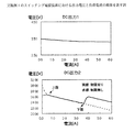
図4に、DC出力1およびDC出力2の負荷電流を横軸に、出力電圧を縦軸とした図を示す。
DC出力1は、出力電圧の状態を一次側の電源制御IC202にフィードバックすることで、負荷電流の変動に対して出力電圧の変動が小さい。
DC出力2は、一次側へのフィードバック制御が無いことから、電圧出力の上下限制限の制御が無い場合、破線で示したような出力特性となる。
本実施例では、図2および図3で示した、抵抗素子213、214および抵抗素子218〜222の組み合わせと、基準電圧設定素子215を選定することで、実線で示したように電圧上昇が上限を超えないように、電圧降下が下限を超えないように抑制できる。これにより、出力の電圧範囲を規定することが可能となる。
FIG. 4 shows a graph in which the load current of
The
DC output 2, since there is no feedback control to the primary side, when there is no control of the upper and lower limit limit the voltage output, an output characteristic as shown by the broken line.
In this embodiment, by selecting the combination of the
以上説明したように、本実施例によれば、DC出力2の出力電圧の上昇制限と降下制限のために1つのダミー抵抗217を共用するこができる。
また、電圧上限の制限動作時には電圧下限の制限動作はなく、逆に電圧下限の制限動作時にも電圧上限の制限動作はない。そのため、単一のダミー抵抗で、安定してかつ安価にかつ容易に制限動作を実現することが可能となる。
As described above, according to the present embodiment, one
In addition, there is no voltage lower limit operation during the voltage upper limit operation, and conversely there is no voltage upper limit operation during the voltage lower limit operation. Therefore, it is possible to realize the limiting operation stably and inexpensively with a single dummy resistor.
図5は、実施例2である“スイッチング電源装置”の構成を表す図である。本実施例は、実施例1の構成において、さらに、DC出力2を停止する構成を追加した例である。 FIG. 5 is a diagram illustrating a configuration of a “switching power supply device” according to the second embodiment. The present embodiment is an example in which a configuration for stopping the DC output 2 is further added to the configuration of the first embodiment.
DC出力2は、スイッチ素子(MOSFET等)300によって出力を行うかどうかを選択し切り換え可能な構成とし、他の出力であるDC出力1によって駆動される負荷1(101)による制御によって選択される。スイッチ素子300は、DC出力2に抵抗素子213が接続されている箇所より上流側、トランスの巻線204d側に接続されている。
The DC output 2 is configured to be switchable by selecting whether or not the output is performed by the switch element (MOSFET or the like) 300, and is selected by control by the load 1 (101) driven by the
DC出力2に接続されている負荷2(102)がDCモータやその他アクチュエータ類であった場合、その負荷に対して電力を供給せず駆動しない場合は、DC出力2の出力は不要であり、かつ電圧出力が停止していて電圧上限を制限する必要がない。このような場合にスイッチ素子300をオフすることによってDC出力2を停止する。
When the load 2 (102) connected to the DC output 2 is a DC motor or other actuators, the output of the DC output 2 is not required when the load 2 (102) is not driven without supplying power to the load. In addition, the voltage output is stopped and there is no need to limit the upper voltage limit. In such a case, the DC output 2 is stopped by turning off the
スイッチ素子300の制御は、負荷1(101)内の不図示の制御装置が行うものとし、例えばワンチップマイコン等で制御するものとする。また同じく負荷2(102)がDCモータやその他アクチュエータ類であった場合、制御線301にて駆動制御も行うものとする。
The
DC出力2の電圧上限を制限しない場合は、図4で示したDC出力2の所定の上限電圧を越えた破線で示した電圧となる。
DC出力2が停止することで、ダミー抵抗217経由でDC出力2より電圧が低いDC出力1へ電流を流し込むかどうかを判断するための、抵抗素子213および214および基準電圧設定素子215への電圧印加はない。また、トランジスタ216を経由してダミー抵抗217へ電流を流し込むこともない。
When the upper limit of the voltage of the DC output 2 is not limited, the voltage is indicated by a broken line exceeding the predetermined upper limit voltage of the DC output 2 shown in FIG.
Voltage to
負荷2(102)への適切な電圧出力が必要であれば、スイッチ素子300をオンすることによってダミー抵抗217への電流供給が可能なように制御できる。
また、負荷2(102)への電流が増加し、DC出力2の出力電圧が所定値以下になった場合、比較器223の出力が反転し、トランジスタ224、225がオンする。これにより、ダミー抵抗217とトランジスタ225を経由してDC出力1の電流が、DC出力1の電圧より低い基準電圧のGNDに流れこむ。そしてトランス204のクロスレギュレーション特性によりDC出力2の出力電圧が上昇するように動作する。
If an appropriate voltage output to the load 2 (102) is required, the
Further, when the current to the load 2 (102) increases and the output voltage of the DC output 2 becomes a predetermined value or less, the output of the
以上説明したように、本実施例によれば、DC出力2の電流が必要でなく、DC出力2の電圧の上限値を制限する必要がない場合に、ダミー抵抗を経由する電流をカットすることができる。また負荷への電流出力が必要な場合のみダミー抵抗を経由する電流を流すことによって適正な出力電圧を設定することができ、無駄な電力消費を防止し、低消費電力化が可能となる。 As described above, according to the present embodiment, when the current of the DC output 2 is not necessary and the upper limit value of the voltage of the DC output 2 does not need to be limited, the current passing through the dummy resistor is cut. Can do. In addition, an appropriate output voltage can be set by flowing a current through a dummy resistor only when current output to the load is necessary, so that wasteful power consumption can be prevented and power consumption can be reduced.
202 電源制御IC
203 一次側スイッチング素子
204 トランス
209 DC出力1フィードバック素子
215 基準電圧設定素子(シャントレギュレータ)
217 ダミー抵抗
223 比較器
202 Power control IC
203 Primary
217
Claims (3)
前記第2の出力が第1所定値以上になった場合に、前記第2の出力をダミー負荷を介して前記第1出力手段に流すことにより前記第2の出力の電圧上昇を制限する電圧上昇制限手段と、
前記第2の出力が前記第1所定値より小さい第2所定値以下になった場合に、前記第1の出力を前記ダミー負荷に流すことにより前記第2の出力電圧の低下を制限する電圧低下制限手段と、を備えたことを特徴とするスイッチング電源装置。 And a secondary or we first output of the transformer first first output means for supplying a load, a second output means for supplying a second output to the second load from the secondary side of the transformer in the provided, by feeding back the first output to the primary side of the transformer, the switching power supply device for controlling the first output according to the output of the feedback,
If the second output is equal to or greater than the first plant value, the voltage that limits the voltage rise of the second output by flowing the second output to the first output means via the dummy load A rise limiting means,
If the second output is below the first plant value smaller than the first plant value, the voltage to limit the decrease of the second output voltage by flowing the first output to the dummy load A switching power supply , comprising: a reduction limiting unit;
前記スイッチ手段は、前記電圧上昇制限手段と前記第2出力手段との接続点より前記トランス側に接続されていることを特徴とする請求項1に記載のスイッチング電源装置。 Previous SL second output comprises a switch means for switching whether to output to the second load,
Said switching means, the switching power supply device according to claim 1, characterized in that said connected to the transformer side of the connection point between the voltage rise limiting means second output means.
前記制御手段によって、前記スイッチ手段の切り換え動作を制御することを特徴とする請求項2に記載のスイッチング電源装置。 Before SL first load is a control means,
The switching power supply device according to claim 2 , wherein the switching means controls the switching operation of the switch means.
Priority Applications (1)
| Application Number | Priority Date | Filing Date | Title |
|---|---|---|---|
| JP2006231975A JP4898351B2 (en) | 2006-08-29 | 2006-08-29 | Switching power supply |
Applications Claiming Priority (1)
| Application Number | Priority Date | Filing Date | Title |
|---|---|---|---|
| JP2006231975A JP4898351B2 (en) | 2006-08-29 | 2006-08-29 | Switching power supply |
Publications (3)
| Publication Number | Publication Date |
|---|---|
| JP2008061301A JP2008061301A (en) | 2008-03-13 |
| JP2008061301A5 JP2008061301A5 (en) | 2009-10-15 |
| JP4898351B2 true JP4898351B2 (en) | 2012-03-14 |
Family
ID=39243452
Family Applications (1)
| Application Number | Title | Priority Date | Filing Date |
|---|---|---|---|
| JP2006231975A Expired - Fee Related JP4898351B2 (en) | 2006-08-29 | 2006-08-29 | Switching power supply |
Country Status (1)
| Country | Link |
|---|---|
| JP (1) | JP4898351B2 (en) |
Families Citing this family (3)
| Publication number | Priority date | Publication date | Assignee | Title |
|---|---|---|---|---|
| JP5191984B2 (en) * | 2009-12-17 | 2013-05-08 | 日本航空電子工業株式会社 | Ring laser gyro device |
| JP5891429B2 (en) * | 2011-06-22 | 2016-03-23 | パナソニックIpマネジメント株式会社 | Power supply |
| CN102420525A (en) * | 2011-12-15 | 2012-04-18 | 南京亚派科技实业有限公司 | Circuit for improving multi-path output cross regulation rate of switching power supply |
Family Cites Families (8)
| Publication number | Priority date | Publication date | Assignee | Title |
|---|---|---|---|---|
| JPS6225872A (en) * | 1985-07-26 | 1987-02-03 | Ricoh Co Ltd | Switching power unit |
| JPH01126163A (en) * | 1987-11-06 | 1989-05-18 | Nec Corp | Non-control system output voltage stabilized circuit in cross regulation |
| JPH04251563A (en) * | 1990-12-28 | 1992-09-07 | Nippon Densan Corp | Switching regulator |
| JPH06113535A (en) * | 1992-09-25 | 1994-04-22 | Tokyo Electric Co Ltd | Transformer coupled dc secondary power supply generating unit |
| JPH11341805A (en) * | 1998-05-26 | 1999-12-10 | Toshiba Corp | Regulated power supply circuit |
| JP2003319649A (en) * | 2002-02-22 | 2003-11-07 | Ricoh Co Ltd | Power circuit for image forming device, and power control method for image forming device |
| JP2004357420A (en) * | 2003-05-29 | 2004-12-16 | Matsushita Electric Ind Co Ltd | Electrical appliance controlling unit |
| JP2005341695A (en) * | 2004-05-26 | 2005-12-08 | Toyota Industries Corp | Flyback-type power supply circuit |
-
2006
- 2006-08-29 JP JP2006231975A patent/JP4898351B2/en not_active Expired - Fee Related
Also Published As
| Publication number | Publication date |
|---|---|
| JP2008061301A (en) | 2008-03-13 |
Similar Documents
| Publication | Publication Date | Title |
|---|---|---|
| JP4391721B2 (en) | Method and apparatus for performing dissipative clamping of electrical circuits | |
| KR100692567B1 (en) | Switching mode power supply and power save mode embodying method thereof | |
| US9564813B2 (en) | Switching power-supply device | |
| KR101889108B1 (en) | Apparatus for power converter reducing the standby power consumption | |
| US7440295B2 (en) | Switching mode power supply with active load detection function, and switching method thereof | |
| JP6171724B2 (en) | LED power supply device and LED lighting device | |
| KR20160021507A (en) | Power conveter and driving method for the same | |
| US9385615B2 (en) | Isolated switching power supply | |
| US9069366B2 (en) | Switching regulator | |
| KR102448640B1 (en) | Power supply with overcurrent protection | |
| JP2010206982A (en) | Switching power supply device | |
| JP4898351B2 (en) | Switching power supply | |
| EP3698456B1 (en) | Ac/dc converter, luminaire and method providing an improved start-up circuit | |
| JP6187024B2 (en) | LED power supply device and LED lighting device | |
| JP2002101662A (en) | Power supply device | |
| US20190222125A1 (en) | Power converter controller, power converter, and corresponding methods | |
| JP2007159305A (en) | Power supply | |
| JP5495679B2 (en) | Power circuit | |
| JP2008067580A (en) | Switching power supply apparatus | |
| KR100840638B1 (en) | Multi output switching power circuit for reducing power consumption in a standby mode | |
| JP2009165323A (en) | Switching power supply device | |
| US20180175727A1 (en) | Boost dc-dc converter and method of using the same | |
| US20050201125A1 (en) | Power circuit restraining rush current | |
| JP2010124648A (en) | Switching power supply apparatus | |
| JP5891429B2 (en) | Power supply |
Legal Events
| Date | Code | Title | Description |
|---|---|---|---|
| A521 | Written amendment |
Free format text: JAPANESE INTERMEDIATE CODE: A523 Effective date: 20090831 |
|
| A621 | Written request for application examination |
Free format text: JAPANESE INTERMEDIATE CODE: A621 Effective date: 20090831 |
|
| A977 | Report on retrieval |
Free format text: JAPANESE INTERMEDIATE CODE: A971007 Effective date: 20111214 |
|
| TRDD | Decision of grant or rejection written | ||
| A01 | Written decision to grant a patent or to grant a registration (utility model) |
Free format text: JAPANESE INTERMEDIATE CODE: A01 Effective date: 20111220 |
|
| A01 | Written decision to grant a patent or to grant a registration (utility model) |
Free format text: JAPANESE INTERMEDIATE CODE: A01 |
|
| A61 | First payment of annual fees (during grant procedure) |
Free format text: JAPANESE INTERMEDIATE CODE: A61 Effective date: 20111226 |
|
| R151 | Written notification of patent or utility model registration |
Ref document number: 4898351 Country of ref document: JP Free format text: JAPANESE INTERMEDIATE CODE: R151 |
|
| FPAY | Renewal fee payment (event date is renewal date of database) |
Free format text: PAYMENT UNTIL: 20150106 Year of fee payment: 3 |
|
| LAPS | Cancellation because of no payment of annual fees |