EP3698456B1 - Ac/dc converter, luminaire and method providing an improved start-up circuit - Google Patents
Ac/dc converter, luminaire and method providing an improved start-up circuit Download PDFInfo
- Publication number
- EP3698456B1 EP3698456B1 EP18782089.9A EP18782089A EP3698456B1 EP 3698456 B1 EP3698456 B1 EP 3698456B1 EP 18782089 A EP18782089 A EP 18782089A EP 3698456 B1 EP3698456 B1 EP 3698456B1
- Authority
- EP
- European Patent Office
- Prior art keywords
- switched mode
- voltage
- power converter
- power supply
- mode power
- Prior art date
- Legal status (The legal status is an assumption and is not a legal conclusion. Google has not performed a legal analysis and makes no representation as to the accuracy of the status listed.)
- Active
Links
- 238000000034 method Methods 0.000 title claims description 5
- 238000004804 winding Methods 0.000 claims description 11
- 230000003213 activating effect Effects 0.000 claims description 2
- 230000001131 transforming effect Effects 0.000 claims 1
- 239000003990 capacitor Substances 0.000 description 2
- 230000001419 dependent effect Effects 0.000 description 1
Images

Classifications
-
- H—ELECTRICITY
- H02—GENERATION; CONVERSION OR DISTRIBUTION OF ELECTRIC POWER
- H02M—APPARATUS FOR CONVERSION BETWEEN AC AND AC, BETWEEN AC AND DC, OR BETWEEN DC AND DC, AND FOR USE WITH MAINS OR SIMILAR POWER SUPPLY SYSTEMS; CONVERSION OF DC OR AC INPUT POWER INTO SURGE OUTPUT POWER; CONTROL OR REGULATION THEREOF
- H02M1/00—Details of apparatus for conversion
- H02M1/36—Means for starting or stopping converters
-
- H—ELECTRICITY
- H02—GENERATION; CONVERSION OR DISTRIBUTION OF ELECTRIC POWER
- H02M—APPARATUS FOR CONVERSION BETWEEN AC AND AC, BETWEEN AC AND DC, OR BETWEEN DC AND DC, AND FOR USE WITH MAINS OR SIMILAR POWER SUPPLY SYSTEMS; CONVERSION OF DC OR AC INPUT POWER INTO SURGE OUTPUT POWER; CONTROL OR REGULATION THEREOF
- H02M3/00—Conversion of dc power input into dc power output
- H02M3/22—Conversion of dc power input into dc power output with intermediate conversion into ac
- H02M3/24—Conversion of dc power input into dc power output with intermediate conversion into ac by static converters
- H02M3/28—Conversion of dc power input into dc power output with intermediate conversion into ac by static converters using discharge tubes with control electrode or semiconductor devices with control electrode to produce the intermediate ac
- H02M3/325—Conversion of dc power input into dc power output with intermediate conversion into ac by static converters using discharge tubes with control electrode or semiconductor devices with control electrode to produce the intermediate ac using devices of a triode or a transistor type requiring continuous application of a control signal
- H02M3/335—Conversion of dc power input into dc power output with intermediate conversion into ac by static converters using discharge tubes with control electrode or semiconductor devices with control electrode to produce the intermediate ac using devices of a triode or a transistor type requiring continuous application of a control signal using semiconductor devices only
- H02M3/33507—Conversion of dc power input into dc power output with intermediate conversion into ac by static converters using discharge tubes with control electrode or semiconductor devices with control electrode to produce the intermediate ac using devices of a triode or a transistor type requiring continuous application of a control signal using semiconductor devices only with automatic control of the output voltage or current, e.g. flyback converters
- H02M3/33523—Conversion of dc power input into dc power output with intermediate conversion into ac by static converters using discharge tubes with control electrode or semiconductor devices with control electrode to produce the intermediate ac using devices of a triode or a transistor type requiring continuous application of a control signal using semiconductor devices only with automatic control of the output voltage or current, e.g. flyback converters with galvanic isolation between input and output of both the power stage and the feedback loop
-
- H—ELECTRICITY
- H05—ELECTRIC TECHNIQUES NOT OTHERWISE PROVIDED FOR
- H05B—ELECTRIC HEATING; ELECTRIC LIGHT SOURCES NOT OTHERWISE PROVIDED FOR; CIRCUIT ARRANGEMENTS FOR ELECTRIC LIGHT SOURCES, IN GENERAL
- H05B45/00—Circuit arrangements for operating light-emitting diodes [LED]
- H05B45/30—Driver circuits
- H05B45/37—Converter circuits
- H05B45/3725—Switched mode power supply [SMPS]
- H05B45/38—Switched mode power supply [SMPS] using boost topology
-
- H—ELECTRICITY
- H05—ELECTRIC TECHNIQUES NOT OTHERWISE PROVIDED FOR
- H05B—ELECTRIC HEATING; ELECTRIC LIGHT SOURCES NOT OTHERWISE PROVIDED FOR; CIRCUIT ARRANGEMENTS FOR ELECTRIC LIGHT SOURCES, IN GENERAL
- H05B45/00—Circuit arrangements for operating light-emitting diodes [LED]
- H05B45/30—Driver circuits
- H05B45/37—Converter circuits
- H05B45/3725—Switched mode power supply [SMPS]
- H05B45/382—Switched mode power supply [SMPS] with galvanic isolation between input and output
-
- H—ELECTRICITY
- H05—ELECTRIC TECHNIQUES NOT OTHERWISE PROVIDED FOR
- H05B—ELECTRIC HEATING; ELECTRIC LIGHT SOURCES NOT OTHERWISE PROVIDED FOR; CIRCUIT ARRANGEMENTS FOR ELECTRIC LIGHT SOURCES, IN GENERAL
- H05B45/00—Circuit arrangements for operating light-emitting diodes [LED]
- H05B45/30—Driver circuits
- H05B45/37—Converter circuits
- H05B45/3725—Switched mode power supply [SMPS]
- H05B45/385—Switched mode power supply [SMPS] using flyback topology
-
- H—ELECTRICITY
- H02—GENERATION; CONVERSION OR DISTRIBUTION OF ELECTRIC POWER
- H02M—APPARATUS FOR CONVERSION BETWEEN AC AND AC, BETWEEN AC AND DC, OR BETWEEN DC AND DC, AND FOR USE WITH MAINS OR SIMILAR POWER SUPPLY SYSTEMS; CONVERSION OF DC OR AC INPUT POWER INTO SURGE OUTPUT POWER; CONTROL OR REGULATION THEREOF
- H02M1/00—Details of apparatus for conversion
- H02M1/0003—Details of control, feedback or regulation circuits
- H02M1/0032—Control circuits allowing low power mode operation, e.g. in standby mode
-
- Y—GENERAL TAGGING OF NEW TECHNOLOGICAL DEVELOPMENTS; GENERAL TAGGING OF CROSS-SECTIONAL TECHNOLOGIES SPANNING OVER SEVERAL SECTIONS OF THE IPC; TECHNICAL SUBJECTS COVERED BY FORMER USPC CROSS-REFERENCE ART COLLECTIONS [XRACs] AND DIGESTS
- Y02—TECHNOLOGIES OR APPLICATIONS FOR MITIGATION OR ADAPTATION AGAINST CLIMATE CHANGE
- Y02B—CLIMATE CHANGE MITIGATION TECHNOLOGIES RELATED TO BUILDINGS, e.g. HOUSING, HOUSE APPLIANCES OR RELATED END-USER APPLICATIONS
- Y02B70/00—Technologies for an efficient end-user side electric power management and consumption
- Y02B70/10—Technologies improving the efficiency by using switched-mode power supplies [SMPS], i.e. efficient power electronics conversion e.g. power factor correction or reduction of losses in power supplies or efficient standby modes
Definitions
- the invention relates to an AC/DC converter with an improved start-up circuit.
- the invention further relates to a luminaire comprising the AC/DC converter with an improved start-up circuit.
- the invention further relates to a method for providing an improved start-up for an AC/DC converter.
- a voltage to the switched mode power converter is required that allows the switch mode power supply to start up. This voltage is provided via a start-up circuit.
- the start-up circuit is a cheap, low efficient circuit.
- a commonly used, simple, embodiment is a starting resistor, bleeder, and a storage capacitor for storing the energy provided to the switched mode power converter. It is common practice to tap the rectified input voltage of the switched mode power converter circuit. This is normally rectified mains which ranges between 120 V RMS and 230 V RMS. The voltage required to start the operation of the switched mode power converter is normally in the range of 10 to 30 V. Therefore, the bleeder has to limit the current from the rectified mains voltage to generate a significant lower voltage which will result in a very low power efficiency.
- US 2017/0070138 discloses that the start-up circuit can be disconnected from the rectified mains when the switched mode power converter has started up. Disconnection is done by a switch that opens when the switched mode power converter has started up. No power is dissipated in the start-up circuit resulting in an increased efficiency of the switched mode power converter.
- the start-up circuit that taps the rectified input voltage comprises high voltage components.
- the additional switch required to turn off the start-up circuit is also a high voltage component. Therefore, the start-up circuit is relatively large and costly. Furthermore, during stand-by operation, the start-up circuit is active and still some power is being dissipated.
- a start-up circuit with an auxiliary power supply for a Gate driver is disclosed in US2003169606
- a start-up circuit with a kick-start power supply for a Gate driver is disclosed in US2015365001 .
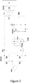
- FIG. 1 shows an example of a commonly used AC/DC converter having a start-up circuit.
- a rectifier bridge RECT comprises diodes D1, D2, D3 and D4 and is coupled to an AC voltage source Vac. This voltage may be the mains voltage. This AC voltage is rectified by the rectifier bridge RECT. The rectified AC voltage Vin is used to provide a voltage to a start-up circuit 3.
- the start-up circuit 3 provides a voltage to an input of the switched mode power converter controller 1. If the voltage exceeds an undervoltage lock-out threshold, the switched mode power converter controller 1 will become active and consequently control the switch SW.
- the undervoltage lock-out threshold can be as high as 10 V to 30 V.
- the switched mode power converter further comprises a transformer T1, the transformer T1 having a primary winding L1 and a secondary winding L2, for providing power to the output.
- a fraction of the output power is provided via connection 2 to the switched mode power converter controller 1.
- a switch SW1 is used to disconnect the start-up circuit 3 from the rectified mains connection to avoid energy losses in the start-up circuit 3 during normal operation of the switched mode power converter.
- the power to the switched mode power converter controller 1 is then provided only via connection 2.
- This connection 2 usually is a connection to an auxiliary winding of the transformer T1. The voltage generated by the auxiliary winding exceeds the undervoltage lock-out threshold voltage and allows the AC/DC converter to keep operating.
- the switch SW1 and the start-up circuit 3 are coupled to the rectified input voltage and therefore high voltage components to withstand mains voltage. These components are relatively large in order to support the high mains voltage and are also relative expensive.
- the invention proposes a different approach wherein a low cost, small kick-start driver 6 is introduced for starting up the switched mode power converter controller 1.
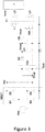
- FIG. 2 shows an example of an AC/DC converter with an improved start-up circuit.
- An input of an auxiliary power supply 4 is coupled to a rectified AC voltage Vin.
- An output of the auxiliary power supply 4 is coupled to an input of a control circuit 5 and to an input of a kick-start power supply 6.
- An output of the kick-start power supply 6 is coupled to an input of a switched mode power converter controller 1.
- An output of the control circuit 5 is coupled to another input of the switched mode power converter controller 1.
- An output of the switched mode power converter controller is coupled to a control terminal of a switch SW.
- the switch SW forms together with an inductor L1 or a transformer T1 a switched mode power supply.
- An output of the switched mode power supply is coupled to a load 7.
- a connection may further be connected to an input of the switched mode power converter controller 1.
- the auxiliary power supply 4 is used to provide a supply voltage Vsup to a control circuit 5.
- the auxiliary power supply 4 is also active when the AC/DC converter is in stand-by mode.
- the control circuit 5 may be arranged to receive a control signal.
- the control circuit 5 may further be configured to control the switched mode power converter controller 1 by e.g. turning it off.
- the control circuit 5 may further control the kick-start power supply 6 by providing a turn on signal Von to the kick-start power supply 6 for turning it on and off.
- the kick-start power supply 6 may be a boost converter.
- the kick-start power supply 6 receives a low voltage provided by the auxiliary power supply 4.
- the auxiliary power supply 4 provides a low voltage to the control circuit 5. This can be in the order of 3.3 V to 5 V for supplying a voltage to e.g. a microcontroller.
- the low voltage that is supplied by the auxiliary power supply 4 is too low to allow the switched mode power converter controller 1 to go in the operating mode. Therefore, the kick-start power supply 6 boosts the voltage supplied by the auxiliary power supply 4 to exceed the minimum required voltage. The boosted voltage is supplied to the switched mode power converter controller 1.
- the voltage is sufficient for the switched mode power converter controller 1 to go into the operating mode and to control the switch SW.
- the switch SW is coupled to at least an inductor, such that they form a switched mode power converter.
- the exemplary switched mode power converter shown in figure 2 is a flyback converter comprising a transformer T1 having a primary side inductor L1, which is magnetically coupled to a secondary side inductor L2. The secondary side is coupled to a load.
- the start-up circuit 3 is always active during standby since the switched mode power supply needs to be activated directly when a control signal Vctl is provided for starting up the switched mode power supply. Therefore, the start-up circuit 3 will always dissipate power during standby.
- the control circuit 5 When the control circuit 5 receives a control signal Vctl, the control circuit 5 will generate a signal for activating the kick-start power supply 6.
- the kick-start power supply 6 will in response to the signal start up and provide a voltage that is larger than the low voltage supplied by the auxiliary power supply 4 and thus larger than the undervoltage lock-out threshold required by the switched mode power converter controller 1 to change the standby mode into the normal operating mode of switched mode power converter 1.
- the capacitor C1 serves as a buffer to stabilize the voltage provided to the switched mode power converter controller 1.
- the switched mode power converter controller 1 in its turn becomes active and starts controlling the switch SW.
- the control circuit 5 may also provide additional signals to the switched mode power converter controller 1. Examples of these signals are dimming signals and turn off signals, which provide additional control possibilities for the switched mode power converter controller 1.
- the switched mode power converter controller 1 controls the switch SW such that a controlled power is provided to the output of the AC/DC converter and the load 7.
- the output voltage Vout or an auxiliary voltage Vaux can be fed back via connection 2 to the switched mode power converter controller 1. This allows the kick-start power supply 6 to turn off, reducing the losses in the AC/DC converter.
- the turn off of the kick-start power supply 6 may be done by sensing the voltage provided to the switched mode power converter controller 1. If the voltage provided via connection 2 is larger than the voltage provided by the kick-start power supply 6, the kick-start power supply will not provide any power and can therefore be turned off.
- control circuit 5 may generate a signal for turning off the switched mode power converter controller 1.
- Figure 3 shows an example of an AC/DC converter comprising an auxiliary output.
- the auxiliary output is shown as an auxiliary winding L3 which provides the start-up voltage Vstart to the switched mode power converter controller 1.
- figure 3 shows an AC/DC converter with an improved start-up circuit. Instead of providing a voltage via connection 2, the voltage is provided via an auxiliary winding L3.
- This auxiliary winding L3 is part of the transformer T1. Diodes D5 and D6 may be placed to prevent power to flow from the auxiliary winding L3 to the kick-start power supply 5 and vice versa.
- the exemplary switched mode power converter in the figures represents a flyback converter. However, many more types of switched mode power supplies are available. Examples are: buck converter, boost convert, buck-boost converter and resonant converter.
- the switched mode power converter is controlled by the switched mode power converter controller 1.
- the control signal Vctl may be send/received wired or wireless between the control circuit 5 and an external control device, such as a remote control.
- the load 7 can be an LED load. LEDs consume a low amount of power. During stand-by, the power consumption is mainly based on stand-by power consumption.
- the start-up circuit 3 in the prior art contributes to the losses during stand-by where the improved kick-start circuit 6 according to the invention does not consume any power during stand-by.
- the kick-start power supply 6 may be any type of voltage boosting circuit.
- the kick-start power supply 6 is a boost converter.
- the switched mode power converter may be any kind of power converter
- the auxiliary winding may also be used as an auxiliary winding magnetically coupled to the inductor of any of the switched mode power converter topologies.
- the AC/DC converter may be equipped with a battery for providing power to the auxiliary power supply 4.
- the battery may be charged by the output of the AC/DC converter or the auxiliary output.
Description
- The invention relates to an AC/DC converter with an improved start-up circuit. The invention further relates to a luminaire comprising the AC/DC converter with an improved start-up circuit. The invention further relates to a method for providing an improved start-up for an AC/DC converter.
- In switched mode power supplies, a voltage to the switched mode power converter is required that allows the switch mode power supply to start up. This voltage is provided via a start-up circuit. When the switched mode power converter has started up, a fraction of the output power of the switched mode power converter can be fed back allowing the switched mode power converter to operate. In general, the start-up circuit is a cheap, low efficient circuit. A commonly used, simple, embodiment is a starting resistor, bleeder, and a storage capacitor for storing the energy provided to the switched mode power converter. It is common practice to tap the rectified input voltage of the switched mode power converter circuit. This is normally rectified mains which ranges between 120 V RMS and 230 V RMS. The voltage required to start the operation of the switched mode power converter is normally in the range of 10 to 30 V. Therefore, the bleeder has to limit the current from the rectified mains voltage to generate a significant lower voltage which will result in a very low power efficiency.
-
US 2017/0070138 discloses that the start-up circuit can be disconnected from the rectified mains when the switched mode power converter has started up. Disconnection is done by a switch that opens when the switched mode power converter has started up. No power is dissipated in the start-up circuit resulting in an increased efficiency of the switched mode power converter. - The start-up circuit that taps the rectified input voltage comprises high voltage components. The additional switch required to turn off the start-up circuit is also a high voltage component. Therefore, the start-up circuit is relatively large and costly. Furthermore, during stand-by operation, the start-up circuit is active and still some power is being dissipated.
- Furthermore, a start-up circuit with an auxiliary power supply for a Gate driver is disclosed in
US2003169606 , and a start-up circuit with a kick-start power supply for a Gate driver is disclosed inUS2015365001 . - It is an objective of the invention to provide a luminaire that has a start-up circuit that is small in size and also very cheap. This object is solved by the features of
device claim 1 and method claim 10. The dependent claims recite advantageous embodiments of the invention. - Examples of the invention will now be described with reference to the accompanying drawings, in which:
-
Fig. 1 shows an example of a prior art AC/DC converter with a start-up circuit. -
Fig. 2 shows an embodiment of the invention. -
Fig. 3 shows a preferred embodiment of the invention. -
Figure 1 shows an example of a commonly used AC/DC converter having a start-up circuit. A rectifier bridge RECT comprises diodes D1, D2, D3 and D4 and is coupled to an AC voltage source Vac. This voltage may be the mains voltage. This AC voltage is rectified by the rectifier bridge RECT. The rectified AC voltage Vin is used to provide a voltage to a start-up circuit 3. The start-up circuit 3 provides a voltage to an input of the switched modepower converter controller 1. If the voltage exceeds an undervoltage lock-out threshold, the switched modepower converter controller 1 will become active and consequently control the switch SW. The undervoltage lock-out threshold can be as high as 10 V to 30 V. The switched mode power converter further comprises a transformer T1, the transformer T1 having a primary winding L1 and a secondary winding L2, for providing power to the output. When the output power is sufficient, a fraction of the output power is provided viaconnection 2 to the switched modepower converter controller 1. A switch SW1 is used to disconnect the start-up circuit 3 from the rectified mains connection to avoid energy losses in the start-up circuit 3 during normal operation of the switched mode power converter. The power to the switched modepower converter controller 1 is then provided only viaconnection 2. Thisconnection 2 usually is a connection to an auxiliary winding of the transformer T1. The voltage generated by the auxiliary winding exceeds the undervoltage lock-out threshold voltage and allows the AC/DC converter to keep operating. - The switch SW1 and the start-
up circuit 3 are coupled to the rectified input voltage and therefore high voltage components to withstand mains voltage. These components are relatively large in order to support the high mains voltage and are also relative expensive. - The invention proposes a different approach wherein a low cost, small kick-
start driver 6 is introduced for starting up the switched modepower converter controller 1. -
Figure 2 shows an example of an AC/DC converter with an improved start-up circuit. An input of anauxiliary power supply 4 is coupled to a rectified AC voltage Vin. An output of theauxiliary power supply 4 is coupled to an input of acontrol circuit 5 and to an input of a kick-start power supply 6. An output of the kick-start power supply 6 is coupled to an input of a switched modepower converter controller 1. An output of thecontrol circuit 5 is coupled to another input of the switched modepower converter controller 1. An output of the switched mode power converter controller is coupled to a control terminal of a switch SW. The switch SW forms together with an inductor L1 or a transformer T1 a switched mode power supply. An output of the switched mode power supply is coupled to aload 7. A connection may further be connected to an input of the switched modepower converter controller 1. Theauxiliary power supply 4 is used to provide a supply voltage Vsup to acontrol circuit 5. Theauxiliary power supply 4 is also active when the AC/DC converter is in stand-by mode. Thecontrol circuit 5 may be arranged to receive a control signal. Thecontrol circuit 5 may further be configured to control the switched modepower converter controller 1 by e.g. turning it off. Thecontrol circuit 5 may further control the kick-start power supply 6 by providing a turn on signal Von to the kick-start power supply 6 for turning it on and off. The kick-start power supply 6 may be a boost converter. The kick-start power supply 6 receives a low voltage provided by theauxiliary power supply 4. This allows that the start-up circuit only needs to provide power during start-up of the switched mode power converter, therefore reducing power dissipation during standby, as will be elucidated in the now following. Theauxiliary power supply 4 provides a low voltage to thecontrol circuit 5. This can be in the order of 3.3 V to 5 V for supplying a voltage to e.g. a microcontroller. The low voltage that is supplied by theauxiliary power supply 4 is too low to allow the switched modepower converter controller 1 to go in the operating mode. Therefore, the kick-start power supply 6 boosts the voltage supplied by theauxiliary power supply 4 to exceed the minimum required voltage. The boosted voltage is supplied to the switched modepower converter controller 1. The voltage is sufficient for the switched modepower converter controller 1 to go into the operating mode and to control the switch SW. The switch SW is coupled to at least an inductor, such that they form a switched mode power converter. The exemplary switched mode power converter shown infigure 2 is a flyback converter comprising a transformer T1 having a primary side inductor L1, which is magnetically coupled to a secondary side inductor L2. The secondary side is coupled to a load. In the prior art, the start-upcircuit 3 is always active during standby since the switched mode power supply needs to be activated directly when a control signal Vctl is provided for starting up the switched mode power supply. Therefore, the start-upcircuit 3 will always dissipate power during standby. - When the
control circuit 5 receives a control signal Vctl, thecontrol circuit 5 will generate a signal for activating the kick-start power supply 6. The kick-start power supply 6 will in response to the signal start up and provide a voltage that is larger than the low voltage supplied by theauxiliary power supply 4 and thus larger than the undervoltage lock-out threshold required by the switched modepower converter controller 1 to change the standby mode into the normal operating mode of switchedmode power converter 1. The capacitor C1 serves as a buffer to stabilize the voltage provided to the switched modepower converter controller 1. The switched modepower converter controller 1 in its turn becomes active and starts controlling the switch SW. - The
control circuit 5 may also provide additional signals to the switched modepower converter controller 1. Examples of these signals are dimming signals and turn off signals, which provide additional control possibilities for the switched modepower converter controller 1. The switched modepower converter controller 1 controls the switch SW such that a controlled power is provided to the output of the AC/DC converter and theload 7. The output voltage Vout or an auxiliary voltage Vaux can be fed back viaconnection 2 to the switched modepower converter controller 1. This allows the kick-start power supply 6 to turn off, reducing the losses in the AC/DC converter. - The turn off of the kick-
start power supply 6 may be done by sensing the voltage provided to the switched modepower converter controller 1. If the voltage provided viaconnection 2 is larger than the voltage provided by the kick-start power supply 6, the kick-start power supply will not provide any power and can therefore be turned off. - Upon receiving another control signal Vctl, the
control circuit 5 may generate a signal for turning off the switched modepower converter controller 1. -
Figure 3 shows an example of an AC/DC converter comprising an auxiliary output. The auxiliary output is shown as an auxiliary winding L3 which provides the start-up voltage Vstart to the switched modepower converter controller 1. Similar tofigure 2 ,figure 3 shows an AC/DC converter with an improved start-up circuit. Instead of providing a voltage viaconnection 2, the voltage is provided via an auxiliary winding L3. This auxiliary winding L3 is part of the transformer T1. Diodes D5 and D6 may be placed to prevent power to flow from the auxiliary winding L3 to the kick-start power supply 5 and vice versa. - The exemplary switched mode power converter in the figures represents a flyback converter. However, many more types of switched mode power supplies are available. Examples are: buck converter, boost convert, buck-boost converter and resonant converter. The switched mode power converter is controlled by the switched mode
power converter controller 1. - The control signal Vctl may be send/received wired or wireless between the
control circuit 5 and an external control device, such as a remote control. - The
load 7 can be an LED load. LEDs consume a low amount of power. During stand-by, the power consumption is mainly based on stand-by power consumption. The start-upcircuit 3 in the prior art contributes to the losses during stand-by where the improved kick-start circuit 6 according to the invention does not consume any power during stand-by. - The kick-
start power supply 6 may be any type of voltage boosting circuit. In an embodiment, the kick-start power supply 6 is a boost converter. - Since the switched mode power converter may be any kind of power converter, it has to be noted that the auxiliary winding may also be used as an auxiliary winding magnetically coupled to the inductor of any of the switched mode power converter topologies.
- Furthermore, the AC/DC converter may be equipped with a battery for providing power to the
auxiliary power supply 4. The battery may be charged by the output of the AC/DC converter or the auxiliary output.
Claims (11)
- A luminaire comprising:- an LED load (7);- an input configured to receive a rectified AC input signal (Vin);- an output configured to provide a controlled output signal (Vout) to the LED load (7);- a switched mode power converter configured to transform the rectified AC input signal (Vin) into the controlled output signal (Vout), wherein the switched mode power converter has an input configured to receive a start-up voltage (Vstart) for changing a stand-by mode of the switched mode power converter into an operating mode of the switched mode power converter by providing the start-up voltage (Vstart) to a switched mode power converter controller (1) coupled to a control terminal of a switch (SW) of the switched mode power converter;- a control circuit (5) configured to receive a control signal (Vctl);- a kick-start power supply (6) configured to receive a switch-on signal (Von) to supply the start-up voltage (Vstart) being larger than a power supply voltage (Vsup),- an auxiliary power supply (4) configured to supply the power supply voltage (Vsup) to the control circuit (5) and the kick-start power supply (6),wherein the control circuit (5) is arranged for activating the switch-on signal (Von) to activate the kick-start power supply (6) for turning the switched mode power converter from the stand-by mode into the operating mode.
- The luminaire according to claim 1 wherein the kick-start power supply (6) is arranged for stopping to supply the start-up voltage when the switched mode power converter has changed into the operating mode.
- The luminaire according to claim 1 wherein the control circuit (5) is arranged for disabling the kick-start power supply after the switched mode power converter has changed into the operating mode.
- The luminaire according to any one of the preceding claims wherein the auxiliary power supply (4) is arranged for drawing power from the rectified AC input signal.
- The luminaire according to claim 1 wherein the auxiliary power supply (4) is arranged for drawing power from a battery.
- The luminaire according to claim 5 wherein the battery is coupled to the controlled output signal (Vout) or an auxiliary output (Vaux) for receiving power.
- The luminaire according to any one of the preceding claims wherein the kick-start power supply (6) comprises a boost converter.
- The luminaire according to claim 6 wherein the start-up voltage is provided to the switched mode power converter by the controlled output signal or the auxiliary output (Vaux), after enabling of the switched mode power converter.
- The luminaire according to any one of the preceding claims wherein the switched mode power converter comprises a transformer (T1) comprising an auxiliary winding (L3) configured to provide the start-up voltage to the switched mode power converter in the operating mode.
- A method for providing a start-up voltage (Vstart) to a switched mode power converter for a luminaire according to claim 1 comprising the steps of:- supplying a power supply voltage (Vsup) to a control circuit (5) and a kick-start power supply (6);- receiving a control signal (Vctl) by the control circuit (5) for turning on the switched mode power converter;- transforming the power supply voltage (Vsup) to a start-up voltage (Vstart), the start-up voltage (Vstart) being larger than the supply voltage (Vsup);- providing the start-up voltage (Vstart) to the switched mode power converter for turning the switched mode power converter from a stand-by mode into an operating mode.
- The method according to claim 10, wherein the provision of the start-up voltage (Vstart) to the switched mode power converter is stopped when the switched mode power converter has started up.
Applications Claiming Priority (2)
| Application Number | Priority Date | Filing Date | Title |
|---|---|---|---|
| EP17196744 | 2017-10-17 | ||
| PCT/EP2018/077636 WO2019076704A1 (en) | 2017-10-17 | 2018-10-10 | Ac/dc converter, luminaire and method providing an improved start-up circuit |
Publications (2)
| Publication Number | Publication Date |
|---|---|
| EP3698456A1 EP3698456A1 (en) | 2020-08-26 |
| EP3698456B1 true EP3698456B1 (en) | 2021-06-30 |
Family
ID=60119926
Family Applications (1)
| Application Number | Title | Priority Date | Filing Date |
|---|---|---|---|
| EP18782089.9A Active EP3698456B1 (en) | 2017-10-17 | 2018-10-10 | Ac/dc converter, luminaire and method providing an improved start-up circuit |
Country Status (5)
| Country | Link |
|---|---|
| US (1) | US10910941B2 (en) |
| EP (1) | EP3698456B1 (en) |
| JP (1) | JP7424970B2 (en) |
| CN (1) | CN111247730A (en) |
| WO (1) | WO2019076704A1 (en) |
Families Citing this family (3)
| Publication number | Priority date | Publication date | Assignee | Title |
|---|---|---|---|---|
| CN111836433A (en) * | 2019-04-22 | 2020-10-27 | 厦门赢科光电有限公司 | Control circuit of power supply |
| CN110996027B (en) * | 2019-12-27 | 2022-07-05 | 深圳康佳电子科技有限公司 | Standby circuit, method and television |
| CN112865497B (en) * | 2021-04-13 | 2022-03-29 | 成都稳海半导体有限公司 | Ramp wave injection circuit free from influence of duty ratio and error compensation method of switching power supply |
Family Cites Families (14)
| Publication number | Priority date | Publication date | Assignee | Title |
|---|---|---|---|---|
| US4737851A (en) | 1987-04-24 | 1988-04-12 | Rca Corporation | On/off control circuitry for television |
| JP3304319B2 (en) * | 1999-09-09 | 2002-07-22 | 阪神エレクトリック株式会社 | Standby power reduction device for electrical equipment with reservation function |
| CN1269297C (en) | 2001-03-06 | 2006-08-09 | 皇家菲利浦电子有限公司 | Start-up circuit for switched mode power supply |
| JP2005210848A (en) | 2004-01-23 | 2005-08-04 | Tdk Corp | Direct-current voltage converter |
| JP4923864B2 (en) | 2006-08-28 | 2012-04-25 | サンケン電気株式会社 | Switching power supply |
| US8527782B2 (en) * | 2008-10-31 | 2013-09-03 | Griffin Technology, Inc. | Power hub |
| US8729811B2 (en) * | 2010-07-30 | 2014-05-20 | Cirrus Logic, Inc. | Dimming multiple lighting devices by alternating energy transfer from a magnetic storage element |
| US8638575B2 (en) * | 2010-08-11 | 2014-01-28 | Fairchild Semiconductor Corporation | High voltage startup circuit |
| JP2012244737A (en) | 2011-05-18 | 2012-12-10 | Panasonic Corp | Led power-supply device |
| WO2013001335A2 (en) | 2011-06-27 | 2013-01-03 | Hap Nguyen | System and method of eliminating wasted energy known as vampire electricity or phantom load loss |
| US20150163874A1 (en) * | 2013-12-11 | 2015-06-11 | General Electric Company | Multi-mode controller circuit |
| US9490711B2 (en) * | 2014-06-12 | 2016-11-08 | Lear Corporation | Gate drive power supply having gate drive voltage supply transformer circuits and kick starter circuit |
| US9812976B2 (en) * | 2015-06-30 | 2017-11-07 | Fairchild Semiconductor Corporation | Control of a startup circuit using a feedback pin of a PWM controller integrated circuit chip |
| JP2017055531A (en) | 2015-09-08 | 2017-03-16 | 株式会社東芝 | Boost converter |
-
2018
- 2018-10-10 US US16/755,627 patent/US10910941B2/en active Active
- 2018-10-10 CN CN201880067478.2A patent/CN111247730A/en active Pending
- 2018-10-10 JP JP2020522001A patent/JP7424970B2/en active Active
- 2018-10-10 EP EP18782089.9A patent/EP3698456B1/en active Active
- 2018-10-10 WO PCT/EP2018/077636 patent/WO2019076704A1/en unknown
Also Published As
| Publication number | Publication date |
|---|---|
| US20200304016A1 (en) | 2020-09-24 |
| WO2019076704A1 (en) | 2019-04-25 |
| JP2020537484A (en) | 2020-12-17 |
| EP3698456A1 (en) | 2020-08-26 |
| JP7424970B2 (en) | 2024-01-30 |
| CN111247730A (en) | 2020-06-05 |
| US10910941B2 (en) | 2021-02-02 |
Similar Documents
| Publication | Publication Date | Title |
|---|---|---|
| US10879806B2 (en) | Voltage converter controller, voltage controller and corresponding methods | |
| JP5554108B2 (en) | Overcurrent prevention type power supply device and lighting fixture using the same | |
| US20080049452A1 (en) | Ultralow Power stan-By Supply | |
| WO2017072940A1 (en) | Swiching power supply device with switchable output voltage setting and integrated circuit for swiching power supply device | |
| JP6430665B2 (en) | LED driver and driving method | |
| EP3698456B1 (en) | Ac/dc converter, luminaire and method providing an improved start-up circuit | |
| US7440295B2 (en) | Switching mode power supply with active load detection function, and switching method thereof | |
| JP3236587B2 (en) | Switching power supply | |
| WO2007063788A1 (en) | Switching power supply device and method for starting same | |
| US8604646B2 (en) | Power management integrated circuit and power management method | |
| US20210203231A1 (en) | Low-power mode for power supply with two-stage driver | |
| US7541691B2 (en) | Standby power supply apparatus | |
| US8129959B1 (en) | Start-up circuitry and method for power converter | |
| KR20120072659A (en) | Switching mode power supply with multiple output | |
| JP7115049B2 (en) | Lighting devices, luminaires and lighting systems | |
| KR102422113B1 (en) | Bidirectional DC-DC converter with improved auxiliary power | |
| JP2017112782A (en) | Switching power supply device | |
| KR102489727B1 (en) | Switching Mode Power Supply for Light-Emitting Diode Lighting Equipment | |
| JP4680453B2 (en) | Switching power supply | |
| JP4637413B2 (en) | Switching power supply | |
| KR101208180B1 (en) | Power supply for reducing standby power | |
| JP2006340471A (en) | Power supply protector | |
| WO2023227456A1 (en) | Connected bulb rc latch optimized for low standby power | |
| JPH0590891U (en) | Lighting device | |
| JP5971227B2 (en) | Switching power supply |
Legal Events
| Date | Code | Title | Description |
|---|---|---|---|
| STAA | Information on the status of an ep patent application or granted ep patent |
Free format text: STATUS: UNKNOWN |
|
| STAA | Information on the status of an ep patent application or granted ep patent |
Free format text: STATUS: THE INTERNATIONAL PUBLICATION HAS BEEN MADE |
|
| PUAI | Public reference made under article 153(3) epc to a published international application that has entered the european phase |
Free format text: ORIGINAL CODE: 0009012 |
|
| STAA | Information on the status of an ep patent application or granted ep patent |
Free format text: STATUS: REQUEST FOR EXAMINATION WAS MADE |
|
| 17P | Request for examination filed |
Effective date: 20200518 |
|
| AK | Designated contracting states |
Kind code of ref document: A1 Designated state(s): AL AT BE BG CH CY CZ DE DK EE ES FI FR GB GR HR HU IE IS IT LI LT LU LV MC MK MT NL NO PL PT RO RS SE SI SK SM TR |
|
| AX | Request for extension of the european patent |
Extension state: BA ME |
|
| GRAP | Despatch of communication of intention to grant a patent |
Free format text: ORIGINAL CODE: EPIDOSNIGR1 |
|
| STAA | Information on the status of an ep patent application or granted ep patent |
Free format text: STATUS: GRANT OF PATENT IS INTENDED |
|
| DAV | Request for validation of the european patent (deleted) | ||
| DAX | Request for extension of the european patent (deleted) | ||
| INTG | Intention to grant announced |
Effective date: 20210120 |
|
| GRAS | Grant fee paid |
Free format text: ORIGINAL CODE: EPIDOSNIGR3 |
|
| GRAA | (expected) grant |
Free format text: ORIGINAL CODE: 0009210 |
|
| STAA | Information on the status of an ep patent application or granted ep patent |
Free format text: STATUS: THE PATENT HAS BEEN GRANTED |
|
| AK | Designated contracting states |
Kind code of ref document: B1 Designated state(s): AL AT BE BG CH CY CZ DE DK EE ES FI FR GB GR HR HU IE IS IT LI LT LU LV MC MK MT NL NO PL PT RO RS SE SI SK SM TR |
|
| REG | Reference to a national code |
Ref country code: CH Ref legal event code: EP |
|
| REG | Reference to a national code |
Ref country code: AT Ref legal event code: REF Ref document number: 1407282 Country of ref document: AT Kind code of ref document: T Effective date: 20210715 |
|
| REG | Reference to a national code |
Ref country code: DE Ref legal event code: R096 Ref document number: 602018019466 Country of ref document: DE |
|
| REG | Reference to a national code |
Ref country code: IE Ref legal event code: FG4D |
|
| REG | Reference to a national code |
Ref country code: LT Ref legal event code: MG9D |
|
| PG25 | Lapsed in a contracting state [announced via postgrant information from national office to epo] |
Ref country code: HR Free format text: LAPSE BECAUSE OF FAILURE TO SUBMIT A TRANSLATION OF THE DESCRIPTION OR TO PAY THE FEE WITHIN THE PRESCRIBED TIME-LIMIT Effective date: 20210630 Ref country code: FI Free format text: LAPSE BECAUSE OF FAILURE TO SUBMIT A TRANSLATION OF THE DESCRIPTION OR TO PAY THE FEE WITHIN THE PRESCRIBED TIME-LIMIT Effective date: 20210630 Ref country code: BG Free format text: LAPSE BECAUSE OF FAILURE TO SUBMIT A TRANSLATION OF THE DESCRIPTION OR TO PAY THE FEE WITHIN THE PRESCRIBED TIME-LIMIT Effective date: 20210930 |
|
| REG | Reference to a national code |
Ref country code: NL Ref legal event code: MP Effective date: 20210630 |
|
| REG | Reference to a national code |
Ref country code: AT Ref legal event code: MK05 Ref document number: 1407282 Country of ref document: AT Kind code of ref document: T Effective date: 20210630 |
|
| PG25 | Lapsed in a contracting state [announced via postgrant information from national office to epo] |
Ref country code: GR Free format text: LAPSE BECAUSE OF FAILURE TO SUBMIT A TRANSLATION OF THE DESCRIPTION OR TO PAY THE FEE WITHIN THE PRESCRIBED TIME-LIMIT Effective date: 20211001 Ref country code: LV Free format text: LAPSE BECAUSE OF FAILURE TO SUBMIT A TRANSLATION OF THE DESCRIPTION OR TO PAY THE FEE WITHIN THE PRESCRIBED TIME-LIMIT Effective date: 20210630 Ref country code: NO Free format text: LAPSE BECAUSE OF FAILURE TO SUBMIT A TRANSLATION OF THE DESCRIPTION OR TO PAY THE FEE WITHIN THE PRESCRIBED TIME-LIMIT Effective date: 20210930 Ref country code: RS Free format text: LAPSE BECAUSE OF FAILURE TO SUBMIT A TRANSLATION OF THE DESCRIPTION OR TO PAY THE FEE WITHIN THE PRESCRIBED TIME-LIMIT Effective date: 20210630 Ref country code: SE Free format text: LAPSE BECAUSE OF FAILURE TO SUBMIT A TRANSLATION OF THE DESCRIPTION OR TO PAY THE FEE WITHIN THE PRESCRIBED TIME-LIMIT Effective date: 20210630 |
|
| PG25 | Lapsed in a contracting state [announced via postgrant information from national office to epo] |
Ref country code: ES Free format text: LAPSE BECAUSE OF FAILURE TO SUBMIT A TRANSLATION OF THE DESCRIPTION OR TO PAY THE FEE WITHIN THE PRESCRIBED TIME-LIMIT Effective date: 20210630 Ref country code: EE Free format text: LAPSE BECAUSE OF FAILURE TO SUBMIT A TRANSLATION OF THE DESCRIPTION OR TO PAY THE FEE WITHIN THE PRESCRIBED TIME-LIMIT Effective date: 20210630 Ref country code: SK Free format text: LAPSE BECAUSE OF FAILURE TO SUBMIT A TRANSLATION OF THE DESCRIPTION OR TO PAY THE FEE WITHIN THE PRESCRIBED TIME-LIMIT Effective date: 20210630 Ref country code: CZ Free format text: LAPSE BECAUSE OF FAILURE TO SUBMIT A TRANSLATION OF THE DESCRIPTION OR TO PAY THE FEE WITHIN THE PRESCRIBED TIME-LIMIT Effective date: 20210630 Ref country code: AT Free format text: LAPSE BECAUSE OF FAILURE TO SUBMIT A TRANSLATION OF THE DESCRIPTION OR TO PAY THE FEE WITHIN THE PRESCRIBED TIME-LIMIT Effective date: 20210630 Ref country code: NL Free format text: LAPSE BECAUSE OF FAILURE TO SUBMIT A TRANSLATION OF THE DESCRIPTION OR TO PAY THE FEE WITHIN THE PRESCRIBED TIME-LIMIT Effective date: 20210630 Ref country code: PT Free format text: LAPSE BECAUSE OF FAILURE TO SUBMIT A TRANSLATION OF THE DESCRIPTION OR TO PAY THE FEE WITHIN THE PRESCRIBED TIME-LIMIT Effective date: 20211102 Ref country code: RO Free format text: LAPSE BECAUSE OF FAILURE TO SUBMIT A TRANSLATION OF THE DESCRIPTION OR TO PAY THE FEE WITHIN THE PRESCRIBED TIME-LIMIT Effective date: 20210630 Ref country code: SM Free format text: LAPSE BECAUSE OF FAILURE TO SUBMIT A TRANSLATION OF THE DESCRIPTION OR TO PAY THE FEE WITHIN THE PRESCRIBED TIME-LIMIT Effective date: 20210630 |
|
| PG25 | Lapsed in a contracting state [announced via postgrant information from national office to epo] |
Ref country code: PL Free format text: LAPSE BECAUSE OF FAILURE TO SUBMIT A TRANSLATION OF THE DESCRIPTION OR TO PAY THE FEE WITHIN THE PRESCRIBED TIME-LIMIT Effective date: 20210630 |
|
| REG | Reference to a national code |
Ref country code: DE Ref legal event code: R097 Ref document number: 602018019466 Country of ref document: DE |
|
| PG25 | Lapsed in a contracting state [announced via postgrant information from national office to epo] |
Ref country code: DK Free format text: LAPSE BECAUSE OF FAILURE TO SUBMIT A TRANSLATION OF THE DESCRIPTION OR TO PAY THE FEE WITHIN THE PRESCRIBED TIME-LIMIT Effective date: 20210630 |
|
| PLBE | No opposition filed within time limit |
Free format text: ORIGINAL CODE: 0009261 |
|
| STAA | Information on the status of an ep patent application or granted ep patent |
Free format text: STATUS: NO OPPOSITION FILED WITHIN TIME LIMIT |
|
| REG | Reference to a national code |
Ref country code: CH Ref legal event code: PL |
|
| PG25 | Lapsed in a contracting state [announced via postgrant information from national office to epo] |
Ref country code: AL Free format text: LAPSE BECAUSE OF FAILURE TO SUBMIT A TRANSLATION OF THE DESCRIPTION OR TO PAY THE FEE WITHIN THE PRESCRIBED TIME-LIMIT Effective date: 20210630 |
|
| 26N | No opposition filed |
Effective date: 20220331 |
|
| REG | Reference to a national code |
Ref country code: BE Ref legal event code: MM Effective date: 20211031 |
|
| PG25 | Lapsed in a contracting state [announced via postgrant information from national office to epo] |
Ref country code: MC Free format text: LAPSE BECAUSE OF FAILURE TO SUBMIT A TRANSLATION OF THE DESCRIPTION OR TO PAY THE FEE WITHIN THE PRESCRIBED TIME-LIMIT Effective date: 20210630 |
|
| PG25 | Lapsed in a contracting state [announced via postgrant information from national office to epo] |
Ref country code: LU Free format text: LAPSE BECAUSE OF NON-PAYMENT OF DUE FEES Effective date: 20211010 Ref country code: IT Free format text: LAPSE BECAUSE OF FAILURE TO SUBMIT A TRANSLATION OF THE DESCRIPTION OR TO PAY THE FEE WITHIN THE PRESCRIBED TIME-LIMIT Effective date: 20210630 Ref country code: BE Free format text: LAPSE BECAUSE OF NON-PAYMENT OF DUE FEES Effective date: 20211031 |
|
| PG25 | Lapsed in a contracting state [announced via postgrant information from national office to epo] |
Ref country code: LI Free format text: LAPSE BECAUSE OF NON-PAYMENT OF DUE FEES Effective date: 20211031 Ref country code: CH Free format text: LAPSE BECAUSE OF NON-PAYMENT OF DUE FEES Effective date: 20211031 |
|
| PG25 | Lapsed in a contracting state [announced via postgrant information from national office to epo] |
Ref country code: IE Free format text: LAPSE BECAUSE OF NON-PAYMENT OF DUE FEES Effective date: 20211010 |
|
| PG25 | Lapsed in a contracting state [announced via postgrant information from national office to epo] |
Ref country code: LT Free format text: LAPSE BECAUSE OF FAILURE TO SUBMIT A TRANSLATION OF THE DESCRIPTION OR TO PAY THE FEE WITHIN THE PRESCRIBED TIME-LIMIT Effective date: 20210630 |
|
| PGFP | Annual fee paid to national office [announced via postgrant information from national office to epo] |
Ref country code: DE Payment date: 20221227 Year of fee payment: 5 |
|
| P01 | Opt-out of the competence of the unified patent court (upc) registered |
Effective date: 20230425 |
|
| PG25 | Lapsed in a contracting state [announced via postgrant information from national office to epo] |
Ref country code: CY Free format text: LAPSE BECAUSE OF FAILURE TO SUBMIT A TRANSLATION OF THE DESCRIPTION OR TO PAY THE FEE WITHIN THE PRESCRIBED TIME-LIMIT Effective date: 20210630 |
|
| PG25 | Lapsed in a contracting state [announced via postgrant information from national office to epo] |
Ref country code: HU Free format text: LAPSE BECAUSE OF FAILURE TO SUBMIT A TRANSLATION OF THE DESCRIPTION OR TO PAY THE FEE WITHIN THE PRESCRIBED TIME-LIMIT; INVALID AB INITIO Effective date: 20181010 |
|
| PGFP | Annual fee paid to national office [announced via postgrant information from national office to epo] |
Ref country code: GB Payment date: 20231024 Year of fee payment: 6 |
|
| PGFP | Annual fee paid to national office [announced via postgrant information from national office to epo] |
Ref country code: FR Payment date: 20231026 Year of fee payment: 6 |