JP4893683B2 - Image display device - Google Patents
Image display device Download PDFInfo
- Publication number
- JP4893683B2 JP4893683B2 JP2008103187A JP2008103187A JP4893683B2 JP 4893683 B2 JP4893683 B2 JP 4893683B2 JP 2008103187 A JP2008103187 A JP 2008103187A JP 2008103187 A JP2008103187 A JP 2008103187A JP 4893683 B2 JP4893683 B2 JP 4893683B2
- Authority
- JP
- Japan
- Prior art keywords
- light
- light emitting
- light receiving
- invisible
- visible light
- Prior art date
- Legal status (The legal status is an assumption and is not a legal conclusion. Google has not performed a legal analysis and makes no representation as to the accuracy of the status listed.)
- Expired - Fee Related
Links
- 238000001514 detection method Methods 0.000 claims description 80
- 239000004973 liquid crystal related substance Substances 0.000 claims description 39
- 239000000758 substrate Substances 0.000 claims description 28
- 230000005540 biological transmission Effects 0.000 claims description 25
- 239000011159 matrix material Substances 0.000 claims description 14
- 230000006870 function Effects 0.000 claims description 8
- 230000015572 biosynthetic process Effects 0.000 claims 1
- 230000003287 optical effect Effects 0.000 claims 1
- 230000002093 peripheral effect Effects 0.000 claims 1
- 239000002210 silicon-based material Substances 0.000 claims 1
- 239000003990 capacitor Substances 0.000 description 21
- 239000011521 glass Substances 0.000 description 19
- 239000010410 layer Substances 0.000 description 17
- 238000000034 method Methods 0.000 description 15
- 238000010586 diagram Methods 0.000 description 11
- 239000012044 organic layer Substances 0.000 description 11
- 238000000295 emission spectrum Methods 0.000 description 10
- 238000012545 processing Methods 0.000 description 10
- 230000008569 process Effects 0.000 description 9
- 230000008859 change Effects 0.000 description 7
- 239000000463 material Substances 0.000 description 7
- 230000000694 effects Effects 0.000 description 6
- 230000007274 generation of a signal involved in cell-cell signaling Effects 0.000 description 4
- 238000013459 approach Methods 0.000 description 3
- 238000005516 engineering process Methods 0.000 description 3
- 230000004044 response Effects 0.000 description 3
- 239000012780 transparent material Substances 0.000 description 3
- 238000006243 chemical reaction Methods 0.000 description 2
- 238000004519 manufacturing process Methods 0.000 description 2
- 229910021421 monocrystalline silicon Inorganic materials 0.000 description 2
- 229920003023 plastic Polymers 0.000 description 2
- XMWRBQBLMFGWIX-UHFFFAOYSA-N C60 fullerene Chemical compound C12=C3C(C4=C56)=C7C8=C5C5=C9C%10=C6C6=C4C1=C1C4=C6C6=C%10C%10=C9C9=C%11C5=C8C5=C8C7=C3C3=C7C2=C1C1=C2C4=C6C4=C%10C6=C9C9=C%11C5=C5C8=C3C3=C7C1=C1C2=C4C6=C2C9=C5C3=C12 XMWRBQBLMFGWIX-UHFFFAOYSA-N 0.000 description 1
- 229910021417 amorphous silicon Inorganic materials 0.000 description 1
- 239000003086 colorant Substances 0.000 description 1
- 238000005401 electroluminescence Methods 0.000 description 1
- 239000010408 film Substances 0.000 description 1
- 229910003472 fullerene Inorganic materials 0.000 description 1
- AMGQUBHHOARCQH-UHFFFAOYSA-N indium;oxotin Chemical compound [In].[Sn]=O AMGQUBHHOARCQH-UHFFFAOYSA-N 0.000 description 1
- 239000000203 mixture Substances 0.000 description 1
- 238000012986 modification Methods 0.000 description 1
- 230000004048 modification Effects 0.000 description 1
- 239000011368 organic material Substances 0.000 description 1
- 229910021420 polycrystalline silicon Inorganic materials 0.000 description 1
- 229920005591 polysilicon Polymers 0.000 description 1
- 150000004032 porphyrins Chemical class 0.000 description 1
- 230000035945 sensitivity Effects 0.000 description 1
- 238000001228 spectrum Methods 0.000 description 1
- 230000003068 static effect Effects 0.000 description 1
- 239000010409 thin film Substances 0.000 description 1
- 238000012546 transfer Methods 0.000 description 1
Images


Description
本発明は、表示面に接触または近接する物体の位置などを検出する機能を備えた画像表示装置に関する。 The present invention relates to an image display device having a function of detecting the position of an object that is in contact with or close to a display surface.
従来より、表示装置の表示面に接触あるいは近接する物体の位置などを検出する技術が知られている。その中でも代表的で一般に広く普及している技術として、タッチパネルを備えた表示装置が挙げられる。 2. Description of the Related Art Conventionally, a technique for detecting the position of an object that touches or approaches a display surface of a display device is known. Among them, a representative and widely used technique is a display device provided with a touch panel.
このタッチパネルも種々のタイプのものが存在するが、一般に普及しているものとして、静電容量を検知するタイプのものが挙げられる。このタイプのものは、指でタッチパネルに接触することでパネルの表面電荷の変化を捕らえ、物体の位置などを検出するようになっている。したがってこのようなタッチパネルを用いることで、ユーザは直感的に操作することが可能である。 There are various types of touch panels, but a type that detects a capacitance is one of the most popular touch panels. This type of device detects changes in the surface charge of the panel by touching the touch panel with a finger, and detects the position of the object. Therefore, the user can operate intuitively by using such a touch panel.
また、最近では表示面上にこのようなタッチパネルを別途設けることなく、物体の位置などを検出することを可能とする技術が各種提案されている。 Recently, various technologies have been proposed that can detect the position of an object without separately providing such a touch panel on the display surface.
例えば、非特許文献1には、低温ポリシリコンを用いて製造した液晶表示装置において各画素に光センサを配置し、物体の映像などを取り込むことができるようにした技術が開示されている。
For example, Non-Patent
上記非特許文献1に記載されている液晶表示装置を利用すれば、取り込んだ映像に基づいて、物体の位置などを検出することも可能である。したがって、このような液晶表示装置を利用することで、表示面上にタッチパネルなどの部品を別途設けることなく、簡易な構成で物体の位置などを検出することが可能となる。
If the liquid crystal display device described in Non-Patent
しかしながら、この液晶表示装置において物体の映像などを取り込む際には、受光する光の輝度は、周囲の環境(明るさ)に左右されることとなる。したがって、周囲が暗い状況下では、取り込んだ映像に基づいて物体の位置などを検出するのが困難となってしまう。ここで、同文献には、Figure5に示されているように、例えば表示面上に指などの物体を接触または近接させ、この物体で反射された表示光を利用することで、周囲が暗い状況下でも物体の位置などを検出することは可能であると記載されている。 However, when capturing an image of an object or the like in this liquid crystal display device, the brightness of the received light depends on the surrounding environment (brightness). Therefore, it becomes difficult to detect the position of an object based on the captured image in a dark environment. Here, as shown in FIG. 5, in the same document, for example, an object such as a finger is brought into contact with or close to the display surface, and the display light reflected by the object is used, so that the surroundings are dark. It is described that it is possible to detect the position of an object even underneath.
しかしながら、このようにして物体で反射された表示光を利用する場合、今度はこの表示光の輝度が問題となる。具体的には、受光する光の輝度が表示光の輝度に左右され、表示光の輝度は画像データに応じて変化することから、例えば表示面がいわゆる黒表示状態のときには、依然として取り込んだ映像に基づいて物体の位置などを検出するのが困難となってしまう。 However, when the display light reflected by the object is used in this way, the brightness of the display light becomes a problem this time. Specifically, the brightness of the received light depends on the brightness of the display light, and the brightness of the display light changes according to the image data. For example, when the display surface is in a so-called black display state, the captured image is still captured. Based on this, it becomes difficult to detect the position of the object.
このように従来の技術では、画像表示装置の表示面に接触または近接する物体を検出するに際して、例えば表示光の輝度などのそのときの使用状況にはよらず、簡易な構成で確実に検出するのは困難であった。 As described above, according to the conventional technology, when detecting an object that is in contact with or close to the display surface of the image display device, the detection is reliably performed with a simple configuration regardless of the current usage state such as the luminance of the display light. It was difficult.
本発明はかかる問題点に鑑みてなされたもので、その目的は、使用状況によらず、簡易な構成で確実に物体の検出を行うことが可能な画像表示装置を提供することにある。 The present invention has been made in view of such problems, and an object of the present invention is to provide an image display device capable of reliably detecting an object with a simple configuration regardless of the usage situation.
本発明の画像表示装置は、非可視光を可視光と共に出射する光源と、表示面内に配置され、可視光を画像データに基づいて変調すると共に非可視光を透過させる複数の液晶素子と、表示面から出射され検出対象物体で反射された非可視光を受光可能な受光素子と、画像データに基づいて液晶素子を表示駆動する表示駆動手段と、受光素子を受光駆動する受光駆動手段と、受光素子から得られた受光信号に基づいて検出対象物体を検出する検出手段とを備えたものである。上記複数の液晶素子は、互いに対向する1対の透明基板間に形成されている。また、1対の透明基板のうちの表示面側の透明基板上における液晶素子の形成領域を除く領域に、光源からの非可視光を選択的に透過すると共に、可視光を遮断するブラックマトリクスとしても機能する非可視光透過フィルタが配設されている。また、上記受光素子は、表示面内における、少なくとも非可視光透過フィルタの形成領域内に配置されている。更に、液晶素子および受光素子がそれぞれ、表示面内にマトリクス状に配置されており、表示駆動手段は、線順次表示動作を行うように液晶素子を表示駆動し、受光駆動手段は、線順次受光動作を行うように受光素子を受光駆動する。 An image display device of the present invention includes a light source that emits invisible light together with visible light, a plurality of liquid crystal elements that are arranged in a display surface, modulate visible light based on image data, and transmit invisible light, A light receiving element capable of receiving invisible light emitted from the display surface and reflected by the detection target object, display driving means for driving the liquid crystal element based on image data, light receiving driving means for driving the light receiving element to receive light, And detecting means for detecting a detection target object based on a light reception signal obtained from the light receiving element. The plurality of liquid crystal elements are formed between a pair of transparent substrates facing each other. As a black matrix that selectively transmits non-visible light from a light source and blocks visible light to a region other than a liquid crystal element forming region on a transparent substrate on the display surface side of a pair of transparent substrates. A non-visible light transmission filter that also functions is provided. The light receiving element is disposed at least in a region where the invisible light transmission filter is formed in the display surface. Further, the liquid crystal elements and the light receiving elements are respectively arranged in a matrix on the display surface, and the display driving means drives the liquid crystal elements to perform a line sequential display operation, and the light receiving driving means receives the line sequential light reception. The light receiving element is driven to receive light so as to operate.
ここで、「非可視光」とは、可視光領域(通常は、400nm〜700nm程度)以外の領域の波長をもつ光を意味する。また、「検出対象物体」とは、表示面に対して接触または近接するように接近している指やポインタ等の物体を意味する。更に、「マトリクス状」とは、複数の液晶素子および複数の受光素子が画像表示装置の表示面全体にわたって、表示面の水平ライン方向および垂直ライン方向に行列配置されている状態を意味し、この配置された各要素を画素と言う。「線順次表示動作」および「線順次受光動作」とは、ある1水平ライン分の各画素に含まれる液晶素子および受光素子がそれぞれ、1水平ラインごとに順次、表示動作および受光動作する態様の動作を意味し、これを画像表示装置の表示面全体にわたって行うことにより、1画面分の画像データの表示および1画面分の各画素についての受光をすることが可能となる。 Here, “ invisible light ” means light having a wavelength in a region other than the visible light region (usually about 400 nm to 700 nm) . Also, the term "detection target object" means an object approaching to have a finger or a pointer such as contact or proximity to the display surface. Furthermore, “matrix” means a state in which a plurality of liquid crystal elements and a plurality of light receiving elements are arranged in a matrix in the horizontal line direction and the vertical line direction of the display surface over the entire display surface of the image display device. Each arranged element is called a pixel. “Line-sequential display operation” and “line-sequential light-receiving operation” are modes in which a liquid crystal element and a light-receiving element included in each pixel for a certain horizontal line sequentially perform a display operation and a light-receiving operation for each horizontal line. This means an operation, and by performing this operation over the entire display surface of the image display device, it is possible to display image data for one screen and receive light for each pixel for one screen.
本発明の画像表示装置では、非可視光が可視光と共に光源から出射され、表示面内に配置された液晶素子において、可視光が画像データに基づいて変調されると共に非可視光が透過する。このとき、表示面に物体(検出対象物体)が接触または近接していると、表示面から出射され検出対象物体で反射された非可視光が、受光素子により受光される。そして、この受光素子から得られた受光信号に基づいて、検出対象物体が検出される。これにより、例えば画像データに応じて輝度変化する表示光など、そのときの使用状況の影響を受けることなく検出対象物体が検出される。 In the image display device of the present invention, invisible light is emitted from the light source together with visible light, and the visible light is modulated and transmitted through the liquid crystal element disposed in the display surface based on the image data. At this time, if an object (detection target object) is in contact with or close to the display surface , the invisible light emitted from the display surface and reflected by the detection target object is received by the light receiving element. A detection target object is detected based on a light reception signal obtained from the light receiving element. As a result, for example, the detection target object is detected without being affected by the use state at that time, such as display light whose luminance changes according to the image data.
本発明の画像表示装置によれば、非可視光を可視光と共に光源から出射し、表示面内に配置された液晶素子において可視光を画像データに基づいて変調すると共に非可視光を透過させ、表示面から出射され検出対象物体で反射された非可視光を受光素子により受光し、この受光素子から得られた受光信号に基づいて検出対象物体を検出するようにしたので、使用状況の影響を受けることなく、確実に物体を検出することができる。また、例えばタッチパネルなどの部品を別途設ける必要もないので、簡易な構成で実現することができる。 According to the image display device of the present invention, invisible light is emitted from the light source together with visible light, and the visible light is modulated based on the image data in the liquid crystal element arranged in the display surface and the invisible light is transmitted. Invisible light emitted from the display surface and reflected by the detection target object is received by the light receiving element, and the detection target object is detected based on the light reception signal obtained from this light receiving element. An object can be reliably detected without receiving it. In addition, since it is not necessary to separately provide components such as a touch panel, it can be realized with a simple configuration.
以下、本発明を実施するための最良の形態(以下、単に実施の形態という。)について、図面を参照して詳細に説明する。なお、以下の実施の形態では、「非可視光領域」を、可視光領域よりも長波長側の領域(近赤外・赤外領域)から構成した場合で説明する。 Hereinafter, the best mode for carrying out the present invention (hereinafter simply referred to as an embodiment) will be described in detail with reference to the drawings. In the following embodiment, a case where the “invisible light region” is configured from a region (near infrared / infrared region) longer than the visible light region will be described.
[第1の実施の形態]
図1は、本発明の第1の実施の形態に係る画像表示装置の全体構成を表すものである。この画像表示装置は、表示部1と、表示信号生成部21と、表示信号保持制御部22と、表示信号ドライバ23と、可視光発光用スキャナ24と、受光用スキャナ31と、受光信号レシーバ32と、受光信号保持部33と、位置検出部34とを備えており、画像データに基づく画像を表示部1に表示すると共に、この表示部1に接触または近接する物体(後述する検出対象物体12)の位置などを検出するものである。なお、本実施の形態に係る物体の検出方法は、本実施の形態に係る画像表示装置によって具現化されるので、以下、併せて説明する。
[First Embodiment]
FIG. 1 shows the overall configuration of an image display apparatus according to the first embodiment of the present invention. The image display device includes a
表示部1は、複数の各画素11が表示部1の全面に渡ってマトリクス状に配置されたLCD(Liquid Crystal Display)からなり、後述するように線順次動作をしながら所定の図形や文字などの画像を表示するものである。また、各画素11は、可視光を発する可視光発光セルCWrgb、非可視光を発する非可視光発光セルCWIR、ならびに可視光および非可視光のいずれをも受光することが可能な受光セルCRを有する発光受光セルCWRから構成され、後述するように画素ごとに発光動作と受光動作とを行うことができるようになっている。なお、この表示部1の構成の詳細については後述する。
The
表示信号生成部21は、例えば図示しないCPU(Central Processing Unit)などから供給される画像データに基づいて、例えば1画面ごと(1フィールドの表示ごと)に表示部1に表示するための表示信号を生成するものである。このようにして生成された表示信号は、表示信号保持制御部22へ出力される。
The display
表示信号保持制御部22は、表示信号生成部21から出力される表示信号を1画面ごと(1フィールドの表示ごと)に、例えばSRAM(Static Random Access Memory)などから構成されるフィールドメモリに格納して保持するものである。この表示信号保持制御部22はまた、各可視光発光セルCWrgbを駆動する可視光発光用スキャナ24および表示信号ドライバ23、ならびに各受光セルCRを駆動する受光用スキャナ31が連動して動作するように制御する役割も果たしている。具体的には、可視光発光用スキャナ24に対しては発光タイミング制御信号41を、受光用スキャナ31に対しては受光タイミング制御信号42を、表示信号ドライバ23に対しては、制御信号、およびフィールドメモリに保持されている1画面分の表示信号に基づく1水平ライン分の表示信号を、それぞれ出力するようになっている。このようにして、これら可視光発光用スキャナ24、受光用スキャナ31および表示信号ドライバ23に各制御信号および表示信号が供給されることで、後述する例えば矢印X方向への線順次動作が行われるようになっている。
The display signal
可視光発光用スキャナ24は、表示信号保持制御部22から出力される発光タイミング制御信号41に応じて、駆動対象の可視光発光セルCWrgbを選択するものである。具体的には、表示部1の各画素11に接続された発光用ゲート線介して駆動対象の可視光発光セルCWrgbへ発光用選択信号を供給し、発光素子選択スイッチを制御するようになっている。このようにして、この発光用選択信号によってある画素の発光素子選択スイッチがオン状態となる電圧が印加されると、その画素では表示信号ドライバ23から供給された電圧に対応した輝度の発光動作がなされるようになっている。
The visible
表示信号ドライバ23は、表示信号保持制御部22から出力される1水平ライン分の表示信号に応じて、駆動対象の可視光発光セルCWrgbへ表示データを供給するものである。具体的には、表示部1の各画素11に接続されたデータ供給線を介して、可視光発光用スキャナ24により選択された画素11へ表示データに対応する電圧を供給するようになっている。このようにして、これら可視光発光用スキャナ24および表示信号ドライバ23が連動して線順次動作することにより、任意の表示データに対応する画像が表示部1に表示されるようになっている。
The
受光用スキャナ31は、表示信号保持制御部22から出力される受光タイミング制御信号42に応じて、駆動対象の受光セルCRを選択するものである。具体的には、表示部1の各画素11に接続された受光用ゲート線を介して駆動対象の受光セルCRへ受光用選択信号を供給し、受光素子選択スイッチを制御するようになっている。つまり、上記した可視光発光用スキャナ24の動作と同様に、受光用選択信号によってある画素の受光素子選択スイッチがオン状態となる電圧が印加されると、その画素から検出された受光信号が受光信号レシーバ32に出力されるようになっている。このようにして、可視光および非可視光が受光セルCRによって受光される。
The
なお、この受光用スキャナ31は、受光信号レシーバ32および受光信号保持部33に対してそれぞれ受光ブロック制御信号43を出力し、これら受光動作に寄与する部分の動作を制御する役割も果たしている。
The light-receiving
受光信号レシーバ32は、受光用スキャナ31から出力される受光ブロック制御信号43に応じて、各受光セルCRから出力された1水平ライン分の受光信号を取得するものである。このようにして取得された1水平ライン分の受光信号は、受光信号保持部33へ出力される。
The light
受光信号保持部33は、受光用スキャナ31から出力される受光ブロック制御信号43に応じて、受光信号レシーバ32から出力される受光信号を1画面ごと(1フィールドの表示ごと)の受光信号に再構成し、例えばSRAMなどから構成されるフィールドメモリに格納して保持するものである。このようにしてフィールドメモリに格納された受光信号は、位置検出部34へ出力される。なお、この受光信号保持部33はメモリ以外の記憶素子から構成されていてもよく、例えば受光信号をアナログデータとして保持しておくようにしてもよい。
The light reception
位置検出部34は、受光信号保持部33から出力される受光信号に基づいて信号処理を行い、受光信号を検出した受光セルCRの位置から、表示部1に接触あるいは近接する物体の位置などを特定するものである。このようにして、表示部1に接触あるいは近接する物体の位置などが特定される。なお、上記のように受光信号保持部33が受光信号をアナログデータとして保持している場合には、この位置検出部34がアナログ/デジタル変換(A/D変換)を行ってから信号処理を実行するように構成することが可能である。
The
なお、表示信号ドライバ23および可視光発光スキャナ24は本発明における「第1発光駆動手段」の一具体例に対応し、受光用スキャナ31は本発明における「第1受光駆動手段」の一具体例に対応する。
The
次に、図2〜図5を参照して、表示部1および発光受光セルCWRの構成の詳細について説明する。
Next, with reference to FIGS. 2-5, the detail of a structure of the
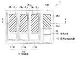
図2は、各画素11における発光受光セルCWRの構成の一例を平面図で表したものである。この発光受光セルCWRは、前述のように可視光発光セルCWrgbと、非可視光発光セルCWIRと、受光セルCRとを有している。また、そのうちの可視光発光セルCWrgbは、赤色発光する赤色発光セルCWrと、緑色発光する緑色発光セルCWgと、青色発光する青色発光セルCWbとを有している。また、赤色発光セルCWrは、赤色発光する部分である赤色発光素子CLrと、この赤色発光素子CLrを駆動するスイッチ素子(後述する発光素子選択スイッチSW1R)を含むTFT(Thin Film Transistor)回路部113Rとを有し、緑色発光セルCWgは、緑色発光する部分である緑色発光素子CLgと、この緑色発光素子CLgを駆動するスイッチ素子(後述する発光素子選択スイッチSW1G)を含むTFT回路部113Gとを有し、青色発光セルCWbは、青色発光する部分である青色発光素子CLbと、この青色発光素子CLbを駆動するスイッチ素子(後述する発光素子選択スイッチSW1B)を含むTFT回路部113Bとを有している。また、非可視光発光セルCWIRは、非可視光を発する部分である非可視光発光素子CLIRを有し、受光セルCRは、可視光および非可視光を受光する部分である受光センサ111と、この受光センサ111を駆動するスイッチ素子(後述する受光素子選択スイッチSW2)を含む受光センサ回路部112とを有している。受光センサ111は、例えばフォトダイオードなどから構成される。ここで、本実施の形態のように可視光領域よりも長波長側の非可視光を利用する場合、この受光センサ111は、アモルファスシリコンよりも単結晶シリコンから構成されていることが好ましい。これは、単結晶シリコンによって受光センサ111を構成したほうが、受光可能な光の波長領域が広くなる(約1100nm以下の波長領域)からである。なお、これら赤色発光素子CLr、緑色発光素子CLgおよび青色発光素子CLbとTFT回路部113との接続関係、ならびにTFT回路部113と前述の表示信号ドライバ23、可視光発光用スキャナ24、受光用スキャナ31および受光信号レシーバ32との接続関係の詳細は後述(図4)する。
FIG. 2 is a plan view showing an example of the configuration of the light emitting / receiving cell CWR in each
ここで、これら赤色発光素子CLr、緑色発光素子CLgおよび青色発光素子CLbは本発明における「第1発光素子」の一具体例に対応し、非可視光発光素子CLIRは本発明における「第2発光素子」の一具体例に対応し、受光センサ111は本発明における「受光素子」の一具体例に対応する。
Here, the red light emitting element CLr, the green light emitting element CLg, and the blue light emitting element CLb correspond to a specific example of the “first light emitting element” in the present invention, and the invisible light emitting element CLIR is the “second light emitting element” in the present invention. The
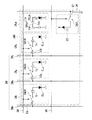
図3は、図2におけるA−A部分の矢視断面図であり、表示部1の断面構成の一例を表したものである。この表示部1は、光源100と、各発光素子(赤色発光素子CLr、緑色発光素子CLg、青色発光素子CLbおよび非可視光発光素子CLIR)を構成する積層構造とから構成されている。この積層構造は、具体的には光源100側から、偏光板101Aと、ガラス基板102Aと、回路部103と、絶縁層104と、透明画素電極105Aと、液晶層106と、透明電極105Bと、カラーフィルタ107と、選択透過フィルタ108と、ブラックマトリクス109と、ガラス基板102Bと、偏光板101Bとから構成されている。すなわち、これら各発光素子は液晶素子から構成され、互いに対向するガラス基板102A,102Bの間に液晶層106を設けた構成となっている。
FIG. 3 is a cross-sectional view taken along the line AA in FIG. 2, and illustrates an example of a cross-sectional configuration of the
光源100は、可視光領域および非可視光領域の光を上記した液晶素子へ向けて発するバックライトである。また、ガラス基板102A,102Bは、いずれもガラス材料からなる透明基板である。ただし、これら102A,102Bをガラス材料の代わりに、透明なプラスチック材料などから構成してもよい。なお、これらガラス基板102A,102Bは本発明における「一対の透明基板」の一具体例であり、そのうちのガラス基板102Bは本発明における「表示面側の透明基板」の一具体例に対応する。
The
回路部103は、図2に示したTFT回路部113や受光センサ回路部112に対応する部分であり、各透明画素電極105Aと電気的に接続されている。また、透明画素電極105Aは各可視光発光セルCWRrgbに配置されており、例えばITO(Indium Tin Oxide;酸化インジウムスズ))などの透明材料から構成される。一方、透明電極105B
は透明電極105Aと対向する共通電極であり、透明電極105Aと同様に例えばITOなどの透明材料から構成される。また、絶縁層104は、各回路部103の間に形成されている。このような構成により、これら透明電極105A,105B間に表示データに応じた電圧が印加され、光源100からのバックライト光LOが液晶層106を透過または遮断されるようになっている。なお、図3に示したように、非可視光発光セルCWIRには、透明画素電極105Aが配置されていない。これは後述するように、非可視光発光セルCWIRからは一定の輝度の非可視光LIRが出射されるようにすればよく、表示データに応じて輝度を変化させる必要がないためである。
The
Is a common electrode facing the
カラーフィルタ107は、各可視光発光セルCWrgb(赤色発光セルCWr、緑色発光セルCWgおよび青色発光セルCWb)に対応する領域に配置されており、液晶層106を透過したバックライト光LOのうち、自己の発光色に対応する波長領域の光を選択的に透過するものである。また、選択透過フィルタ108は、非可視光発光セルCWIRに対応する領域に配置されており、液晶層106を透過したバックライト光LOのうち、非可視光領域(ここでは、可視光領域よりも長波長側の領域)の光を選択的に透過するものである。ブラックマトリクス109は、各カラーフィルタ107および選択透過フィルタ108の間に配置されており、光源100からのバックライト光LOを遮断して表示面10側に出射しないようにするものである。
The
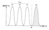
このようにして、光源100からのバックライト光LOがカラーフィルタ107または選択透過フィルタ108を透過することで、可視光発光セルCWrgbからは可視光Lrgb、すなわち、赤色発光セルCWrからは赤色光Lrが、緑色発光セルCWgからは緑色光Lgが、青色発光セルCWbからは青色光Lbがそれぞれ出射される一方、非可視光発光セルCWIRからは非可視光LIRが出射されるようになっている。したがって、これら可視光Lrgbおよび非可視光LIRの発光スペクトルは、例えば図4に示したようになる。すなわち、しきい値波長W1よりも短波長側である可視光領域側には、赤色発光スペクトルPr、緑色発光スペクトルPgおよび青色発光スペクトルPbからなる可視光発光スペクトルPrgbが、そしてしきい値波長W1よりも長波長側である非可視光領域には、非可視光発光スペクトルPIRが、それぞれ観測されるようになっている。なお、カラーフィルタ107は本発明における「第1選択透過フィルタ」の一具体例に対応し、選択透過フィルタ108は本発明における「第2選択透過フィルタ」の一具体例に対応する。
In this way, the backlight light LO from the
図5は、各画素11における発光受光セルCWRの回路構成の一例を表したものである。この発光受光セルCWRは、前述のように、赤色発光セルCWr、緑色発光セルCWgおよび青色発光セルCWbからなる可視光発光セルCWrgbと、非可視光発光セルCWIRと、受光セルCRとを有している。このうち、可視光発光セルCWrgbには、表示信号ドライバ23に接続された表示データ供給線DWと、可視光発光用スキャナ24に接続された発光用ゲート線GWとが接続されている。具体的には、赤色発光セルCWrには表示データ供給線DWrと発光用ゲート線GWとが、緑色発光セルCWgには表示データ供給線DWgと発光用ゲート線GWとが、青色発光セルCWbには表示データ供給線DWbと発光用ゲート線GWとが、それぞれ接続されている。一方、受光セルCRには、受光用スキャナ31に接続された受光用ゲート線GRと受光信号レシーバ32に接続されたデータ読み出し線DRとが接続され、非可視光発光セルCWIRには、これらの接続線は接続されていない。なお、この非可視光発光セルCWIRに接続線が接続されていないのは、前述のように非可視光発光セルCWIRからは一定の輝度の非可視光LIRが出射されるようにすればよく、表示データに応じて輝度を変化させる必要がないためである。
FIG. 5 illustrates an example of a circuit configuration of the light emitting / receiving cell CWR in each
赤色発光セルCWrは、前述の赤色発光素子CLrと、前述のTFT回路部113R内に設けられた発光素子選択スイッチSW1Rとを有している。緑色発光セルCWgは、前述の緑色発光セルCLgと、前述のTFT回路部113G内に設けられた発光素子選択スイッチSW1Gとを有している。青色発光セルCWbは、前述の青色発光素子CLbと、前述のTFT回路部113B内に設けられた発光素子選択スイッチSW1Bとを有している。また、受光セルCRは、前述の受光素子としての受光センサ111(図5に示した例では、フォトダイオード)と、前述の受光センサ回路部112内に設けられた受光素子選択スイッチSW2とを有している。また、非可視光発光セルCWIRは、前述の非可視光発光素子CLIRと、定電圧電源VIRとを有している。なお、これら発光素子選択スイッチSW1R,SW1G,SW1Bは、いずれも例えばTFTなどのスイッチ素子から構成される。
The red light emitting cell CWr includes the above-described red light-emitting element CLr and the light-emitting element selection switch SW1R provided in the above-described
発光素子選択スイッチSW1R,SW1G,SW1Bはそれぞれ、発光用ゲート線GWによってそのオンオフ動作が制御されるようになっている。また、発光素子選択スイッチSW1Rの一端は表示データ供給線DWrに接続され、その他端は赤色発光素子CLrの一端(具体的には、前述の透明画素電極105A)に接続され、赤色発光素子CLrの他端(具体的には、前述の透明電極105B)は接地されている。同様に、発光素子選択スイッチSW1Gの一端は表示データ供給線DWgに接続され、その他端は緑色発光素子CLgの一端に接続され、緑色発光素子CLgの他端は接地されている。発光素子選択スイッチSW1Bの一端は表示データ供給線DWbに接続され、その他端は青色発光素子CLbの一端に接続され、青色発光素子CLbの他端は接地されている。一方、受光素子選択スイッチSW2は受光用ゲート線GRによってそのオンオフ動作が制御されるようになっており、その一端はデータ読出線DRに接続され、その他端は受光センサ111の一端に接続され、受光センサ111の他端は接地または正バイアス点(図示せず)に接続されている。また、非可視光発光素子CLIRの一端(具体的には、図3の回路部103側)は、非可視光発光用データ供給線DWIRを介して定電圧電源VIRに接続され、その他端(具体的には、前述の透明電極105B)は接地されている。
The on / off operations of the light emitting element selection switches SW1R, SW1G, SW1B are controlled by the light emitting gate line GW. Further, one end of the light emitting element selection switch SW1R is connected to the display data supply line DWr, and the other end is connected to one end of the red light emitting element CLr (specifically, the above-described
このような回路構成により発光受光セルCWRでは、以下のような発光動作および受光動作がなされる。 With such a circuit configuration, the light emitting / receiving cell CWR performs the following light emitting operation and light receiving operation.
まず、可視光Lrgbの発光動作時には、発光用ゲート線GWから供給される発光用選択信号に応じて、1水平ライン分の発光素子選択スイッチSW1R,SW1G,SW1Bがそれぞれオン状態となる。そして各表示信号に応じた輝度の発光となるよう、表示データ供給線DWr,DWg,DWbからそれぞれI1r,I1g,I1bの経路にて、赤色発光素子CLr、緑色発光素子CLgおよび青色発光素子CLbが充電されることで、これら発光素子はそれぞれ、各発光色に対応すると共に各表示信号に応じた輝度からなる発光動作を行う。これに対して、非可視光LIRの発光動作については、定電圧電源VIRから非可視光発光用データ供給線DWIRを介して非可視光発光素子CLIRへ常に一定の電圧が印加されることから、常に一定の電流がI1IRの経路にて非可視光発光素子CLIRが充電され、非可視光発光素子CLIRは、一定の輝度からなる非可視光LIRの発光動作を行う。 First, during the light emission operation of the visible light Lrgb, the light emitting element selection switches SW1R, SW1G, and SW1B for one horizontal line are turned on according to the light emission selection signal supplied from the light emission gate line GW. The red light-emitting element CLr, the green light-emitting element CLg, and the blue light-emitting element CLb are respectively connected to the display data supply lines DWr, DWg, and DWb from the display data supply lines DWr, DWg, and DWb through the paths I1r, I1g, and I1b, respectively. By being charged, each of these light emitting elements performs a light emitting operation corresponding to each light emission color and having a luminance corresponding to each display signal. On the other hand, in the light emission operation of the invisible light LIR, a constant voltage is always applied from the constant voltage power source VIR to the invisible light emitting element CLIR through the invisible light emission data supply line DWIR. The invisible light emitting element CLIR is always charged through a path of constant current I1IR, and the invisible light emitting element CLIR performs a light emitting operation of invisible light LIR having a constant luminance.
一方、受光動作時には、受光用ゲート線GRから供給される受光用選択信号に応じて、1水平ライン分の受光素子選択スイッチSW2がオン状態となり、受光センサ111において受光した光量に応じた電流がI2の経路にてデータ読出線DRへ供給されることで、可視光Lrgbおよび非可視光LIRの受光動作を行うようになっている。
On the other hand, during the light receiving operation, the light receiving element selection switch SW2 for one horizontal line is turned on according to the light receiving selection signal supplied from the light receiving gate line GR, and a current corresponding to the amount of light received by the
なお、発光動作および受光動作のいずれの動作も行っていないときには、発光素子選択スイッチSW1R,SW1G,SW1Bおよび受光素子選択スイッチSW2のいずれのスイッチもオフ状態となっており、表示データ供給線DWr,DWg,DWbと赤色発光素子CLr、緑色発光素子CLgまたは青色発光素子CLbとの間の接続、ならびにデータ読出線DRと受光センサ111との間の接続は、いずれも切断されるようになっている。
When neither the light emitting operation nor the light receiving operation is performed, all the light emitting element selection switches SW1R, SW1G, SW1B and the light receiving element selection switch SW2 are in the off state, and the display data supply lines DWr, The connections between DWg and DWb and the red light emitting element CLr, the green light emitting element CLg or the blue light emitting element CLb, and the connection between the data read line DR and the
次に、以上のような構成からなる画像表示装置において、表示部1の表示面10に接触あるいは近接する物体(検出対象物体)を検出する処理を、黒表示状態の場合とそれ以外の通常表示状態の場合とに分けて説明する。
Next, in the image display device configured as described above, processing for detecting an object (detection target object) that is in contact with or close to the
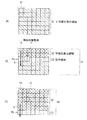
まず、図6〜図8を参照して、検出対象物体を検出する処理の概要について説明する。ここで図6は、通常表示状態のときに検出対象物体を線順次動作で検出する処理の一例を表したものである。一方、図7は、黒表示状態のときの表示部1の状況を断面図で表したものであり、図8は、同じく黒表示状態のときに検出対象物体を線順次動作で検出する処理の一例を表したものである。なお、黒表示状態とは、通常、表示部1の画素11から可視光Lrgbが出射されていない状態を意味するが、ここでは説明のために、表示部1に表示されている映像が、全ての画素11にわたって黒表示である状態を示すものとする。また、図6および図8に示した1マスは、表示部1における画素11を表している。
First, an outline of processing for detecting a detection target object will be described with reference to FIGS. FIG. 6 shows an example of processing for detecting the detection target object by line sequential operation in the normal display state. On the other hand, FIG. 7 is a sectional view showing the state of the
まず、図6を参照して、通常表示状態の場合について説明する。 First, the case of the normal display state will be described with reference to FIG.
図6(A)に示したように、非可視光発光素子CLIRからは常に一定の輝度からなる非可視光LIRが出射されることから、表示部1における各画素11は常に非可視光発光領域51となっている。
As shown in FIG. 6A, since the invisible light LIR having a constant luminance is always emitted from the invisible light emitting element CLIR, each
ここで、図6(B),(C)に示したように、前述の1水平ライン分の可視光発光素子CLrgbの発光動作(可視光発光領域52の領域)、および1水平ライン分の受光センサ111の受光動作(受光領域53の領域)が、それぞれ矢印Xのように同期して線順次動作(それぞれ、線順次発光動作および線順次受光動作)を行うことで、表示部1全体にわたってそれぞれ、映像の表示(可視光Lrgbの出射)ならびに可視光Lrgbおよび非可視光LIRの受光が可能となる。そして、例えば表示部1に指などの検出対象物体12が接触あるいは近接すると、可視光発光領域52から出射された可視光Lrgbおよび非可視光発光領域51から出射された非可視光LIRが、それぞれこの検出対象物体12で反射される。ここで、この可視光Lrgbまたは非可視光LIRを出射した画素と位置が近い画素(例えば、図6(B)の符号P3で示した水平ラインの画素)には、この検出対象物体12での反射光が入射する一方、位置が遠い画素(例えば、図6(C)の符号P6で示した水平ラインの画素)には、この検出対象物体12での反射光は入射しない。したがって、ある検出対象物体12の近傍に位置する受光センサ111からは受光信号が検出される一方、それ以外の領域からは受光信号が検出されないことから、この検出対象物体12が表示部1のどの位置に存在するのかが検知できる。
Here, as shown in FIGS. 6B and 6C, the light emission operation (region of the visible light emitting region 52) of the visible light emitting element CLrgb for one horizontal line described above and the light reception for one horizontal line are performed. The light receiving operation of the sensor 111 (the region of the light receiving region 53) performs a line sequential operation (respectively, a line sequential light emitting operation and a line sequential light receiving operation) in synchronization with each other as indicated by an arrow X, so that each of the
このようにして、1水平ラインが線順次発光動作すると共にその可視光Lrgbまたは非可視光LIRの出射光による反射光を線順次受光動作することにより、表示部1全体が発光領域になると共に受光領域となり、ある画像データが表示部1全体に渡って表示されることに加え、受光センサ111から検出された受光信号により、ある検出対象物体12が表示部1の近傍に存在するかどうか、そして存在する場合はその位置が検出される。
In this way, one horizontal line performs a line-sequential light emission operation, and a line-sequential light-receiving operation is performed on the reflected light of the visible light Lrgb or the invisible light LIR. In addition to displaying certain image data over the
また、黒表示状態の場合には、上記のように全ての画素11で黒表示となることから、図7に示したように、光源100から出射されたバックライト光LOは、各可視光発光セルCWr,CWg,CWbにおいては、液晶層106で遮断される。一方、非可視光発光セルCWIRでは、前述のように常に一定の輝度からなる非可視光LIRが出射されることから、光源100から出射されたバックライト光LOは、液晶層106を透過することとなる。したがって、このような黒表示状態のときでも、図8(A)〜(C)に示したように、この非可視光領域51から出射された非可視光LIRを用いることで、図6に示した通常表示状態の場合と同様にして、検出対象物体12の位置が検出される。このようにして、表示部1の表示状態、すなわち画像データに応じた輝度変化の影響や、さらに例えば周囲の状況(明るい場合や暗い場合など)など、そのときの使用状況の影響を受けることなく、検出対象物体12の位置が検出される。
Further, in the black display state, all the
次に、図9を参照して、図1の画像表示装置において検出対象物体12を検出する処理の詳細を、やはり通常表示状態の場合と黒表示状態の場合とに分けて説明する。ここで図9は、図1の画像表示装置において検出対象物体12を検出する処理をタイミング図で表したものであり、(A)は表示データ供給線DWiを、(B)は非可視光発光用データ供給線DWIRを、(C)は1〜n番目の水平ラインの発光用ゲート線GW(GW1〜GWn)を、(D)は1〜n番目の水平ラインの受光用ゲート線GR(GR1〜GRn)を、(E)は1〜n番目の水平ラインにおける1垂直ライン分の発光受光セルCWRi(CWRi1〜CWRin)を、(F)は各発光受光セルCWRiに接続されたデータ読出線DRiを、それぞれ示している。また、図9において位置を表す符号であるi,j,n,mは、ある自然数を表している。
Next, with reference to FIG. 9, the details of the process of detecting the
また、図9において、横軸は時間を表し、垂直期間TH1,THmは表示部1の画面全体分スキャンするのに要する時間、つまり可視光発光用スキャナ24および受光用スキャナ31がそれぞれ、GW1〜GWnまでおよびGR1〜GRnまでスキャンする時間を表すものである。また、検出対象物体12は表示部1における発光受光セルCWRi(j-1),CWRij,CWRi(j+1)付近にあるものとし、これに対応する期間、つまり垂直期間TH1においてはタイミングt3〜t6の期間(受光信号検出期間TF1)において、同様に垂直期間THmにおいては受光信号検出期間TFmにおいて受光信号が検出されるものとする。一方、縦軸は上記の(A)〜(D),(F)に示した各信号の各タイミングにおける電圧を表している。ここで、(A)に示した表示データ供給線DWiの信号は、各画素11において任意の輝度に対応する表示データであり、垂直期間TH1では通常表示状態、垂直期間THmでは黒表示状態であることを表している。また、(E)に示したのは、各発光受光セルCWRiにおける可視光Lrgbの発光と可視光Lrgbおよび非可視光LIRの受光とを行う発光受光期間TRW、ならびに可視光Lrgbの発光期間TWを表すものである。
In FIG. 9, the horizontal axis represents time, and the vertical periods TH1 and THm are the time required for scanning the entire screen of the
なお、図9に示した処理は、可視光発光用スキャナ24による発光動作のスキャンおよび受光用スキャナ31による受光動作のスキャンが同じタイミングで同一の水平ラインによって線順次動作していく例であるが、可視光Lrgbの発光動作スキャンおよび受光動作スキャンは、独立して動作することが可能である。また、(F)に示したデータ読出線DRiの信号は、アナログデータとして受光信号保持部33に格納される例であるが、前述のようにデジタルデータとして受光信号保持部33に格納するように構成することも可能である。
The processing shown in FIG. 9 is an example in which the light emission operation scan by the visible
まず、通常表示状態の場合(垂直期間TH1)について説明する。 First, the case of the normal display state (vertical period TH1) will be described.
タイミングt0〜t1では、全ての発光用ゲート線GWおよび受光用ゲート線GRに選択信号が供給されず、各発光受光セルCWRiにおける発光素子選択スイッチSW1および受光素子選択スイッチSW2は、いずれもオフ状態となる。したがって、表示データ供給線DWr,DWg,DWbと赤色発光素子CL、緑色発光素子CLgまたは青色発光素子CLbとの間の接続、ならびにデータ読出線DRと受光センサ111との間の接続は切断され、各発光受光セルCWRiは非動作状態となる。一方、可視光発光用データ線DWIRには常に一定の電圧が印加され、一定の輝度からなる非可視光LIRが出射されている。
At timings t0 to t1, selection signals are not supplied to all the light emitting gate lines GW and the light receiving gate lines GR, and both the light emitting element selection switch SW1 and the light receiving element selection switch SW2 in each light emitting / receiving cell CWRi are in the off state. It becomes. Therefore, the connection between the display data supply lines DWr, DWg, DWb and the red light emitting element CL, the green light emitting element CLg, or the blue light emitting element CLb, and the connection between the data read line DR and the
次にタイミングt1〜t2において、発光用ゲート線GW1および受光用ゲート線GR1には発光用選択信号および受光用選択信号が供給され、これらのゲート線が接続された発光受光セルCWR11,CWR21,…,CWRm1における発光素子選択スイッチSW1および受光素子選択スイッチSW2が、一斉にオン状態となる。またこのとき、図9中に発光受光期間TRWで示したように、各発光受光セルCWRiにおいて、各可視光発光素子CLr,CLg,CLbが表示データ供給線DWiの信号に応じた輝度の発光動作を行うと共に、受光センサ111において受光された光量に応じた電流がデータ読出線DRiへ供給されることで、受光動作がなされる。なお、この期間(タイミングt1〜t2)では、検出対象物体12による受光信号が検出されないことから、データ読出線DRiからも出力信号は出力されない。
Next, at timings t1 to t2, a light emission selection signal and a light reception selection signal are supplied to the light emission gate line GW1 and the light reception gate line GR1, and the light emission light reception cells CWR11, CWR21,. , CWRm1, the light emitting element selection switch SW1 and the light receiving element selection switch SW2 are simultaneously turned on. At this time, as indicated by the light emission / reception period TRW in FIG. 9, in each light-emission / reception cell CWRi, each visible light-emitting element CLr, CLg, CLb emits light with a luminance corresponding to the signal of the display data supply line DWi. And a current corresponding to the amount of light received by the
また、タイミングt2以降も同様にして、発光用ゲート線GW2および受光用ゲート線GR2,発光用ゲート線GW3および受光用ゲート線GR3,…と、線順次に発光動作および受光動作が行われるが、やはり検出対象物体12による受光信号が検出されないので、データ読出線DRiからは出力信号が出力されない。なお、各発光受光セルCWRiとも、発光受光期間TRWが終了した後は、ある一定期間、発光動作期間TWが保持される。
Similarly, after the timing t2, the light emission operation and the light reception operation are performed in order of light emission gate line GW2, light reception gate line GR2, light emission gate line GW3, light reception gate line GR3,. Again, since a light reception signal from the
タイミングt3〜t6において、検出対象物体12からの反射光が、各発光受光セルCWRi(j-1),CWRij,CWRi(j+1)において受光されると、受光した光量に応じた電流が電圧に変換され、データ読出線DRiへ出力される(受光信号検出期間TF1)。なお、この場合、各発光受光セルCWRi(j-1),CWRij,CWRi(j+1)では、自己の発光動作に基づく反射光、および非可視光発光セルCWIRからの出射光による反射光の両者が受光されることとなるので、データ読出線DRiへ出力される信号は、表示データ供給線DWiおよび非可視光発光用データ供給線DWIRにおける信号に応じた値となる。
At timings t3 to t6, when the reflected light from the
タイミングt6〜7も、タイミングt1〜t3と同様に、発光用ゲート線GWj+2および受光用ゲート線GRj+2,発光用ゲート線GWj+3および受光用ゲート線GRj+3,…,発光用ゲート線GWnおよび受光用ゲート線GRnと、線順次に発光動作および受光動作が行われるが、やはり検出対象物体12による受光信号が検出されないので、データ読出線DRiからは出力信号が出力されない。
Similarly to the timings t1 to t3, the light emission gate
このようにして、垂直期間TH1において、発光受光セルCWRi(j-1),CWRij,CWRi(j+1)付近の位置に検出対象物体12が存在すると検出することできる。
In this way, it is possible to detect that the
一方、黒表示状態の場合(垂直期間THm)のときも、基本的には通常表示状態の場合(垂直期間TH1)と同様に動作する。つまり、各発光受光セルCWRiにおいて、各可視光発光素子CLr,CLg,CLbが発光動作を行うと共に、受光センサ111において受光された光量に応じた電流がデータ読出線DRiへ供給され、受光動作がなされる。ただし、この黒表示状態では、表示データ供給線DWiの信号に応じた輝度がほぼ0であることから、受光センサ111では、非可視光発光セルCWIRからの出射光による反射光のみが受光される。つまり、各発光受光セルCWRi(j-1),CWRij,CWRi(j+1)は非可視光発光セルCWIRからの出射光による反射光のみを受光することになるので、データ読出線DRiへ出力される信号は、非可視光発光用データ供給線DWIRにおける信号に応じた値となる。このようにして、黒表示状態の垂直期間THmにおいても、受光信号検出期間TFmにおいてデータ読出線DRiから出力信号が出力され、やはり発光受光セルCWRi(j-1),CWRij,CWRi(j+1)付近の位置に検出対象物体12が存在すると検出される。
On the other hand, in the black display state (vertical period THm), the operation is basically the same as in the normal display state (vertical period TH1). That is, in each light emitting / receiving cell CWRi, each visible light emitting element CLr, CLg, CLb performs a light emitting operation, and a current corresponding to the amount of light received by the
以上のように、本実施の形態によれば、表示部1の表示面10から非可視光LIRを出射すると共に、この表示面10に接触または近接する検出対象物体12で反射された非可視光LIRを表示面10上で受光し、受光したこの非可視光LIRに基づいて検出対象物体12の検出を行うようにしたので、表示部1の表示状態、すなわち画像データに応じた輝度変化の影響や、さらに例えば周囲の状況(明るい場合や暗い場合など)など、そのときの使用状況の影響を受けることなく、確実に検出することができる。
As described above, according to the present embodiment, the invisible light LIR is emitted from the
また、このような検出対象物体12の位置などを検出するうえで、例えばタッチパネルなどの部品を別途設ける必要もないので、簡易な構成で実現することができる。
In addition, when detecting the position of the
また、受光セルCR内の受光センサ111が、非可視光LIRだけではなく可視光Lrgbをも受光するようにしたので、本実施の形態で説明してきた物体の検出処理に加え、例えば画像の取り込み処理を行うことができ、例えばスキャナとして利用することも可能となる。
Since the
また、可視光および非可視光を出射することが可能な光源100と、カラーフィルタ107および選択透過フィルタ108とを組み合わせて構成したので、各可視光発光セルCWr,CWg,CWbからは可視光Lrgbを、非可視光発光セルCWIRからは非可視光LIRを、それぞれ別個に出射することができる。なお、このように可視光および非可視光を出射することが可能な光源100の代わりに、可視光を出射することが可能な光源(第1光源)と、非可視光を出射することが可能な光源(第2光源)とを別個に設けるように構成してもよい。
Further, since the
また、非可視光発光セルCWIRからは、常に一定の輝度で非可視光LIRを出射するようにしたので、各可視光発光セルCWr,CWg,CWbや受光セルCRに設けられているような選択スイッチが不要となり、発光受光セルCWRの構成を簡素化することが可能となる。 Further, since the invisible light LIR is always emitted from the invisible light emitting cell CWIR with a constant luminance, the selection as provided in each of the visible light emitting cells CWr, CWg, CWb and the light receiving cell CR is possible. A switch is not required, and the configuration of the light emitting / receiving cell CWR can be simplified.
なお、本実施の形態では、図2に示したように、画素11内において、各可視光発光セルCWr,CWg,CWbと非可視光発光セルCWIRおよび受光セルCRとが並列配置されている場合の例について説明してきたが、例えば図10に示したように、画素11内において、非可視光発光セルCWIRおよび受光セルCRを各可視光発光セルCWr,CWg,CWbの下部や上部に配置するようにしてもよい。
In the present embodiment, as shown in FIG. 2, in the
また、本実施の形態では、選択透過フィルタ108を非可視光発光セルCWIRに対応する領域のみに配置し、受光センサ111が非可視光LIRおよび可視光Lrgbの両者を受光する場合の例について説明してきたが、例えば図11(A)に示したように、選択透過フィルタ108を受光センサ111に対応する領域にも配置し、この受光センサ111が非可視光LIRのみを受光するようにしてもよい。このように構成した場合、可視光Lrgbの影響を取り除くことができるので、より確実に検出対象物体12を検出することができる。また、例えば図11(B)に示したように、受光セルCR内に受光センサを複数(この場合、2つ)設け、非可視光LIRおよび可視光Lrgbの両者を受光する受光センサ111Aと、非可視光LIRのみを受光する111Bとに区別し、これら受光センサ111A,111Bを選択的に受光駆動するようにしてもよい。このように構成した場合、例えば本実施の形態で説明したような検出対象物体12の検出処理と、前述の映像取り込み処理とを、自由に切り換えることが可能となる。なお、この受光センサ111A上に、可視光Lrgbのみを選択的に透過するフィルタを設け、受光センサ111Aが可視光Lrgbのみを受光するようにしてもよく、この場合のこの受光センサ111Aは本発明における「第1受光素子」の一具体例に対応し、受光センサ111Bは本発明における「第2受光素子」の一具体例に対応する。
In the present embodiment, an example in which the
また、例えば図12に示したように、非可視光LIRのみを選択的に透過する選択透過フィルタ108を、各画素11内において、各可視光発光セルCWr,CWg,CWbに対応する領域以外の領域全てに配置するようにしてもよい。このように構成した場合、各可視光発光セルCWr,CWg,CWbに対応する領域以外からは、可視光Lrgbが出射されないことから、選択透過フィルタ108が、図3に示したブラックマトリクス109としての役割を果たすことが可能となる。よって、図3に示した表示部1の積層構造において、積層数を1層減らすことができることから、製造工程を簡素化することができ、製造コストを削減することが可能となる。
For example, as shown in FIG. 12, a
また、可視光発光用スキャナ24に対して受光用スキャナ31が間引いて(2本おきや3本おきに)駆動するようにしてもよい。そのように構成した場合、本実施の形態における効果に加え、受光信号のデータ量を削減することで受光側の回路(受光用スキャナ311、受光信号レシーバ32、受光信号保持部33)を簡素化することができ、また、低消費電力化を図ることも可能となる。よって、特に接触あるいは近接する物体の検出位置の精度よりも回路構成の簡素化および低消費電力化を図りたい場合には有効である。
Further, the
また、複数の可視光発光セルCWr,CWg,CWbが出射した光を複数の受光セルCRが受光し、それらの受光信号を加算して1つの受光信号として出力するようにしてもよい。そのように構成した場合、第1の実施の形態における効果に加え、受光信号のデータ量を削減することで受光側の回路(受光用スキャナ31、受光信号レシーバ32および受光信号保持部33)を簡素化することができ、また、低消費電力化を図ることも可能となる。またその場合、複数の受光信号を加算し、1つの受光信号として受光信号レシーバ32に出力することになるので、出力信号量を上げてS/N比を向上させ、検出感度を上げることも可能となる。
Alternatively, the light emitted from the plurality of visible light emitting cells CWr, CWg, and CWb may be received by the plurality of light receiving cells CR, and the light reception signals may be added and output as one light reception signal. In such a configuration, in addition to the effects of the first embodiment, the light receiving side circuit (
また、各可視光発光セルCWr,CWg,CWbに対して受光セルCRの配置自体を間引くように構成にしてもよい。そのように構成した婆、第1の実施の形態における効果に加え、受光信号のデータ量を削減することで受光側の回路(受光用スキャナ31、受光信号レシーバ32、受光信号保持部33)を簡素化することができ、また、低消費電力化を図ることも可能となる。また逆に、各可視光発光セルCWr,CWg,CWbに対して複数の受光セルCRを配置するようにしてもよい。そのように構成した場合、第1の実施の形態における効果に加え、接触あるいは近接する物体をより精度良く位置検出することが可能となる。
Further, the arrangement may be such that the arrangement of the light receiving cells CR is thinned out for each of the visible light emitting cells CWr, CWg, and CWb. In addition to the effects of the first embodiment, the light receiving signal circuit (
[第2の実施の形態]
次に、本発明の第2の実施の形態について説明する。
[Second Embodiment]
Next, a second embodiment of the present invention will be described.
上記の第1の実施の形態では、各発光素子(赤色発光素子CLr、緑色発光素子CLg、青色発光素子CLbおよび非可視光発光素子CLIR)が、いずれも液晶素子から構成されている場合について説明したが、本実施の形態では、各発光素子が、いずれも自発光素子である有機EL(ElectroLuminescence)素子から構成されている場合について説明する。 In the first embodiment, the case where each light emitting element (red light emitting element CLr, green light emitting element CLg, blue light emitting element CLb, and invisible light emitting element CLIR) is composed of a liquid crystal element will be described. However, in the present embodiment, a case will be described in which each light emitting element is composed of an organic EL (ElectroLuminescence) element that is a self-luminous element.
図13は、本実施の形態に係る画像表示装置の全体構成を表すものである。この図において、図1に示した第1の実施の形態に係る画像表示装置の構成要素と同一の構成要素には同一の符号を付し、適宜説明を省略する。この画像表示装置は、図1に示した第1の実施の形態における表示部1に代えて、表示部6を備えたものである。
FIG. 13 shows the overall configuration of the image display apparatus according to the present embodiment. In this figure, the same components as those of the image display device according to the first embodiment shown in FIG. 1 are denoted by the same reference numerals, and description thereof will be omitted as appropriate. This image display device includes a
表示部6は、表示部1と同様に、複数の各画素61が全面に渡ってマトリクス状に配置され、線順次動作をしながら所定の図形や文字などの画像を表示するものである。また、画素61は、画素11と同様に、可視光を発する可視光発光セルCWrgb、非可視光を発する非可視光発光セルCWIR、ならびに可視光および非可視光のいずれをも受光することが可能な受光セルCRを有する発光受光セルCWRから構成されている。この表示部6が表示部1と異なるのは、上記のように、各発光素子(赤色発光素子CLr、緑色発光素子CLg、青色発光素子CLbおよび非可視光発光素子CLIR)を有機EL素子から構成するようにした点である。
Similar to the
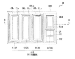
図14は、各画素61における発光受光セルCWRの構成の一例を平面図で表したものであり、第1の実施の形態における図2に対応するものである。本実施の形態の発光受光セルCWRは、前述のように可視光発光セルCWrgbと、非可視光発光セルCWIRと、受光セルCRとを有している。また、そのうちの可視光発光セルCWrgbは、赤色発光する赤色発光セルCWrと、緑色発光する緑色発光セルCWgと、青色発光する青色発光セルCWbとを有している。また、赤色発光セルCWrは、赤色発光する部分である赤色発光素子ELrと、この赤色発光素子ELrを駆動するスイッチ素子(後述する発光素子選択スイッチSW3R)を含むTFT回路部613Rとを有し、緑色発光セルCWgは、緑色発光する部分である緑色発光素子ELgと、この緑色発光素子ELgを駆動するスイッチ素子(後述する発光素子選択スイッチSW3G)を含むTFT回路部613Gとを有し、青色発光セルCWbは、青色発光する部分である青色発光素子ELbと、この青色発光素子ELbを駆動するスイッチ素子(後述する発光素子選択スイッチSW3B)を含むTFT回路部613Bとを有している。また、非可視光発光セルCWIRは、非可視光を発する部分である非可視光発光素子ELIRと、この非可視光発光素子ELIRへ電荷を供給する容量素子(後述するキャパシタCIR)を含むTFT回路部613IRとを有し、受光セルCRは、受光センサ111と、この受光センサ111を駆動する受光素子選択スイッチSW2を含む受光センサ回路部112とを有している。なお、赤色発光素子ELr、緑色発光素子ELgおよび青色発光素子ELbはそれぞれ、本発明における「赤色発光有機EL素子」、「緑色発光有機EL素子」および「青色発光有機EL素子」の一具体例に対応する。また、非可視光発光素子ELIRは、本発明における「非可視光発光有機EL素子」の一具体例に対応する。
FIG. 14 is a plan view showing an example of the configuration of the light emitting / receiving cell CWR in each
図15は、図14におけるB−B部分の矢視断面図であり、表示部6の断面構成の一例を表したものであり、第1の実施の形態における図3に対応するものである。この表示部6は、各発光素子(赤色発光素子ELr、緑色発光素子ELg、青色発光素子ELbおよび非可視光発光素子ELIR)を構成する積層構造から構成されている。また、この積層構造は具体的には、ガラス基板602Aと、回路部603と、コンタクト部601と、絶縁層604と、画素電極605Aと、有機層606と、透明電極605Bと、ガラス基板602Bとから構成されている。すなわち、これら各発光素子は上記のように有機EL素子から構成され、互いに対向するガラス基板602A,602Bの間に有機層606を設けた構成となっている。
FIG. 15 is a cross-sectional view taken along the line B-B in FIG. 14, showing an example of a cross-sectional configuration of the
ガラス基板602A,602Bは、ガラス基板102A,102Bと同様に、いずれもガラス材料からなる透明基板である。ただし、これら602A,602Bをガラス材料の代わりに、透明なプラスチック材料などから構成してもよい。なお、これらガラス基板602A,602Bは本発明における「一対の基板」の一具体例であり、そのうちのガラス基板602Bは本発明における「表示面側の基板」の一具体例に対応する。
The
回路部603は、図14に示したTFT回路部613や受光センサ回路部112に対応する部分であり、コンタクト部601を介して各画素電極605Aと電気的に接続されている。また、この画素電極605Aは、各可視光発光セルCWRrgbに配置されている。一方、透明電極605Bは透明電極605Aと対向する共通電極であり、例えばITOなどの透明材料から構成される。
The
有機層606は、所定の有機材料から構成されており、画素電極605Aおよび透明電極605B間に表示データに応じた電圧が印加されると、材料の組成に応じた所定の波長領域の光を、印加された電圧に応じた輝度で発光するものである。具体的には、可視光発光セルCWRrにおける有機層606は赤色光Lrを、可視光発光セルCWRgにおける有機層606は緑色光Lgを、可視光発光セルCWRbにおける有機層606は青色光Lbを出射する一方、非可視光発光セルCWIRにおける有機層606は非可視光LIRを出射するようになっている。この非可視光発光セルCWIRにおける有機層606は、例えばポルフィリン・フラーレン膜の電荷移動錯体などから構成することができる。なお、各可視光発光セルCWRrgbにおける有機層606は、本発明における「発光層」の一具体例に対応し、非可視光発光セルCWRIRにおける有機層606は、本発明における「非可視光発光層」の一具体例に対応する。
The
図16は、各画素61における発光受光セルCWRの回路構成の一例を表したものであり、第1の実施の形態における図5に対応するものである。第1の実施の形態の各画素11における発光受光セルと異なるのは、各可視光発光セルCWrgb内の構成である。具体的には、赤色発光セルCWrは、前述の赤色発光素子ELrと、前述のTFT回路部613R内に設けられた発光素子選択スイッチSW3Rと、電荷保持用のキャパシタCrとを有している。緑色発光セルCWgは、前述の緑色発光セルELgと、前述のTFT回路部613G内に設けられた発光素子選択スイッチSW3Gと、電荷保持用のキャパシタCgとを有している。青色発光セルCWbは、前述の青色発光素子ELbと、前述のTFT回路部613B内に設けられた発光素子選択スイッチSW3Bと、電荷保持用のキャパシタCbとを有している。また、非可視光発光セルCWIRは、前述の非可視光発光素子ELIRと、定電圧電源VIRと、電荷保持用のキャパシタCIRとを有している。なお、これら発光素子選択スイッチSW3R,SW3G,SW3Bは、いずれも発光素子選択スイッチSW1R,SW1G,SW1Bと同様に、例えばTFTなどのスイッチ素子から構成される。
FIG. 16 illustrates an example of a circuit configuration of the light-emitting / receiving cell CWR in each
発光素子選択スイッチSW3R,SW3G,SW3Bはそれぞれ、発光用ゲート線GWによってそのオンオフ動作が制御されるようになっている。また、発光素子選択スイッチSW3Rの一端は表示データ供給線DWrに接続され、その他端はキャパシタCrの一端に接続され、キャパシタCrの他端は赤色発光素子ELrの一端(具体的には、前述の画素電極605A)に接続され、赤色発光素子ELrの他端(具体的には、前述の透明電極605B)は接地されている。同様に、発光素子選択スイッチSW3Gの一端は表示データ供給線DWgに接続され、その他端はキャパシタCgの一端に接続され、キャパシタCgの他端は緑色発光素子ELgの一端に接続され、緑色発光素子ELgの他端は接地されている。発光素子選択スイッチSW3Bの一端は表示データ供給線DWbに接続され、その他端はキャパシタCbの一端に接続され、キャパシタCbの他端は青色発光素子ELbの一端に接続され、青色発光素子ELbの他端は接地されている。また、非可視光発光素子CLIRの一端(具体的には、前述の画素電極605A)は、非可視光発光用データ供給線DWIRおよびキャパシタCIRを介して定電圧電源VIRに接続され、その他端(具体的には、前述の透明電極605B)は接地されている。
The on / off operations of the light emitting element selection switches SW3R, SW3G, and SW3B are controlled by the light emitting gate line GW. One end of the light emitting element selection switch SW3R is connected to the display data supply line DWr, the other end is connected to one end of the capacitor Cr, and the other end of the capacitor Cr is one end of the red light emitting element ELr. The other end of the red light emitting element ELr (specifically, the above-described
このような回路構成により、本実施の形態の発光受光セルCWRでは、以下のような発光動作がなされる。なお、受光動作については、第1の実施の形態と同様であるので、その説明を省略する。 With such a circuit configuration, the light emitting / receiving cell CWR of the present embodiment performs the following light emitting operation. Since the light receiving operation is the same as that of the first embodiment, the description thereof is omitted.
まず、可視光Lrgbの発光動作時には、発光用ゲート線GWから供給される発光用選択信号に応じて、1水平ライン分の発光素子選択スイッチSW3R,SW3G,SW3Bがそれぞれオン状態となる。そして各表示信号に応じた輝度の発光となるよう、表示データ供給線DWr,DWg,DWbからそれぞれI3r,I3g,I3bの経路にて、キャパシタCr,Cg,Cbに電荷が充電される。そしてこれらキャパシタCr,Cg,Cbに充電された電荷が赤色発光素子CLr、緑色発光素子CLgおよび青色発光素子CLbへそれぞれ供給されることで電流が流れ、これら発光素子はそれぞれ、各発光色に対応すると共に各表示信号に応じた輝度からなる発光動作を行う。これに対して、非可視光LIRの発光動作については、定電圧電源VIRから非可視光発光用データ供給線DWIRを介してキャパシタCIRに常に一定の電圧が印加されることから、非可視光発光素子CLIRへは常に一定の電流がI3IRの経路にて流れ、非可視光発光素子CLIRは、一定の輝度からなる非可視光LIRの発光動作を行う。 First, during the light emission operation of the visible light Lrgb, the light emitting element selection switches SW3R, SW3G, and SW3B for one horizontal line are turned on according to the light emission selection signal supplied from the light emission gate line GW. The capacitors Cr, Cg, and Cb are charged through the paths I3r, I3g, and I3b from the display data supply lines DWr, DWg, and DWb, respectively, so as to emit light with luminance corresponding to each display signal. Then, currents flow when the charges charged in the capacitors Cr, Cg, and Cb are respectively supplied to the red light emitting element CLr, the green light emitting element CLg, and the blue light emitting element CLb, and these light emitting elements correspond to the respective emission colors. At the same time, a light emission operation having a luminance corresponding to each display signal is performed. On the other hand, in the light emission operation of the invisible light LIR, a constant voltage is always applied to the capacitor CIR from the constant voltage power source VIR through the invisible light emission data supply line DWIR. A constant current always flows through the I3IR path to the element CLIR, and the invisible light emitting element CLIR performs a light emitting operation of invisible light LIR having a constant luminance.
なお、発光動作および受光動作のいずれの動作も行っていないときには、発光素子選択スイッチSW3R,SW3G,SW3Bおよび受光素子選択スイッチSW2のいずれのスイッチもオフ状態となっており、表示データ供給線DWr,DWg,DWbと赤色発光素子ELr、緑色発光素子ELgまたは青色発光素子ELbとの間の接続、ならびにデータ読出線DRと受光センサ111との間の接続は、いずれも切断されるようになっている。
When neither the light emitting operation nor the light receiving operation is performed, all of the light emitting element selection switches SW3R, SW3G, SW3B and the light receiving element selection switch SW2 are in the OFF state, and the display data supply lines DWr, The connections between DWg and DWb and the red light emitting element ELr, the green light emitting element ELg or the blue light emitting element ELb, and the connection between the data readout line DR and the
本実施の形態における検出対象物体の検出方法は、第1の実施の形態における検出対象物体の検出方法と基本的に同様であり、異なるのは、駆動する各発光素子が、液晶素子の代わりに有機EL素子となっている点である。したがって、図6〜図9に示した第1の実施の形態の場合と同様、通常表示状態の場合、受光素子検出期間TF1において受光信号が得られることで、発光受光セルCWRi(j-1),CWRij,CWRi(j+1)付近の位置に検出対象物体12が存在すると検出される。
The detection target object detection method in the present embodiment is basically the same as the detection target object detection method in the first embodiment, except that each light emitting element to be driven is replaced with a liquid crystal element. This is an organic EL element. Therefore, as in the case of the first embodiment shown in FIGS. 6 to 9, in the normal display state, the light receiving signal is obtained in the light receiving element detection period TF1, and thus the light emitting / receiving cell CWRi (j−1). , CWRij, CWRi (j + 1), it is detected that the
また、例えば図17に示したような黒表示状態(非可視光発光セルCWIRのみから、非可視光LIRが出射されている状態)においても、やはり第1の実施の形態の場合と同様に、受光素子検出期間TFmにおいて受光信号が得られることで、検出対象物体12の位置が検出される。
Further, for example, in the black display state as shown in FIG. 17 (the state where the invisible light LIR is emitted only from the invisible light emitting cell CWIR), as in the case of the first embodiment, By obtaining a light reception signal in the light receiving element detection period TFm, the position of the
以上のように、本実施の形態によれば、各発光素子(可視光発光素子ELr,ELg,ELbおよび非可視光発光素子ELIR)を自発光素子である有機EL素子から構成したとしても、第1の実施の形態と同様、使用状況の影響を受けることなく、確実に検出対象物体12を検出することができる。
As described above, according to the present embodiment, even if each light emitting element (visible light emitting element ELr, ELg, ELb, and invisible light emitting element ELIR) is composed of an organic EL element that is a self-emitting element, As in the first embodiment, the
なお、例えば図18に示したように、非可視光発光セルCWIRを非可視光発光素子ELIRの代わりに、白色発光素子ELLOと、前述の選択透過フィルタ108との組み合わせにより構成するようにしてもよい。ここで、この白色発光素子ELLOは本発明における「白色発光有機EL素子」の一具体例に対応し、この場合の非可視光発光セルCWIRは本発明における「白色発光層」の一具体例に対応する。このように構成した場合でも、非可視光発光セルCWIRから、非可視光LIRを出射することができる。また、例えば図19に示したように、各可視光発光セルCWrgbにおいても、前述のカラーフィルタ107を設けるようにしてもよい。このように構成した場合、各可視光発光素子ELr,ELg,ELbから出射される可視光Lrgbの色純度を高めることができる。
For example, as shown in FIG. 18, the invisible light emitting cell CWIR may be configured by a combination of the white light emitting element ELLO and the
さらに、例えば図20に示したように、各可視光発光セルCWrgbを、白色発光素子ELLOとカラーフィルタ107との組み合わせにより構成するようにしてもよく、また、例えば図21に示したように、非可視光発光セルCWIRおよび各可視光発光セルCWrgbの両者を、白色発光素子ELLOと、選択透過フィルタ108またはカラーフィルタ107との組み合わせにより構成するようにしてもよい。このように構成した場合でも、各可視光発光セルCWrgbから各可視光Lrgbを出射すると共に、非可視光発光セルCWIRから非可視光LIRを出射することができる。
Further, for example, as shown in FIG. 20, each visible light emitting cell CWrgb may be configured by a combination of a white light emitting element ELLO and a
なお、本実施の形態では、自発光素子の一例として、各発光素子(赤色発光素子CLr、緑色発光素子CLg、青色発光素子CLbおよび非可視光発光素子CLIR)を有機EL素子から構成した場合について説明してきたが、他の自発光素子、例えば発光ダイオード(LED;Light Emitting Diode)から構成してもよい。 In this embodiment, as an example of the self-light-emitting element, each light-emitting element (red light-emitting element CLr, green light-emitting element CLg, blue light-emitting element CLb, and invisible light-emitting element CLIR) is configured from an organic EL element. As described above, other self-light emitting elements such as light emitting diodes (LEDs) may be used.
また、本実施の形態においても、第1の実施の形態の場合と同様に、各発光受光セルCWRの配置や構成を任意に設定することが可能であり、また、種々の発光駆動または受光駆動を行うことが可能である。 Also in the present embodiment, as in the case of the first embodiment, the arrangement and configuration of each light emitting / receiving cell CWR can be arbitrarily set, and various light emission driving or light receiving driving can be performed. Can be done.
[第3の実施の形態]
次に、本発明の第3の実施の形態について説明する。
[Third Embodiment]
Next, a third embodiment of the present invention will be described.
上記の第1および第2の実施の形態では、非可視光の発光素子と非可視光(および可視光)の受光素子とを別々に構成(非可視光発光素子CLIRおよび受光センサ111)した場合について説明してきたが、本実施の形態では、このような非可視光の発光素子と非可視光(および可視光)の受光素子とを単一の素子(非可視光発光素子ELIR)で構成した場合について説明する。 In the first and second embodiments described above, the invisible light emitting element and the invisible light (and visible light) light receiving element are configured separately (the invisible light emitting element CLIR and the light receiving sensor 111). In this embodiment, the invisible light emitting element and the invisible light (and visible light) light receiving element are configured by a single element (invisible light emitting element ELIR). The case will be described.
図22は、本実施の形態に係る画像表示装置の全体構成を表すものである。この図において、図1に示した第1の実施の形態に係る画像表示装置または図13に示した第2の実施の形態に係る画像表示装置の構成要素と同一の構成要素には同一の符号を付し、適宜説明を省略する。この画像表示装置は、図1,図13に示した第1または第2の実施の形態における表示部1,6に代えて表示部7を設けると共に、受光用スキャナ31の代わりに、受光信号選択スキャナ35を設けるようにしたものである。なお、本実施の形態における表示信号ドライバ23および可視光発光スキャナ24は、本発明における「第3発光駆動手段」の一具体例に対応し、受光信号選択スキャナ35は、本発明における「第4発光駆動手段」および「第2受光駆動手段」の一具体例に対応する。
FIG. 22 illustrates the overall configuration of the image display apparatus according to the present embodiment. In this figure, the same components as those of the image display device according to the first embodiment shown in FIG. 1 or the image display device according to the second embodiment shown in FIG. The description is omitted as appropriate. This image display device is provided with a display unit 7 instead of the
表示部7は、表示部1,6と同様に、複数の各画素71が全面に渡ってマトリクス状に配置され、線順次動作をしながら所定の図形や文字などの画像を表示するものである。この画素71が表示部1,6と異なるのは、発光受光セルCWRを、可視光を発する可視光発光セルCWrgbと、非可視光の発光と非可視光(および可視光)の受光とを併有する非可視光発光受光セルCWRIRとから構成するようにした点である。すなわち、表示部1,6における可視光発光セルCWIRおよび受光セルCRの機能を、非可視光発光受光セルCWRIRにもたせるようにした点である。
Similar to the
受光信号選択スキャナ35は、表示信号保持制御部22から出力される受光タイミング制御信号42に応じて、非可視光発光受光セルCWRIRの発光動作と受光動作とを切り換え、それにより受光駆動対象の非可視光発光受光セルCWRIRを選択するものである。具体的には後述するように、表示部7の各画素71に接続された切換線Sを介して切換信号を供給し受光信号選択スキャナ35は、受光用スキャナ31と同様に、受光信号レシーバ32および受光信号保持部33に対してそれぞれ受光ブロック制御信号43を出力し、これら受光動作に寄与する部分の動作を制御する役割も果たしている。
The light reception
図23は、各画素71における発光受光セルCWRの構成の一例を平面図で表したものであり、第1の実施の形態における図2、および第2の実施の形態における図14に対応するものである。本実施の形態の発光受光セルCWRは、前述のように可視光発光セルCWrgbと、非可視光発光受光セルCWRIRとを有している。そのうちの非可視光発光受光セルCWRIRは、非可視光の発光と非可視光(および可視光)の受光とを併有する部分である非可視光発光素子ELIRを有している。この非可視光発光セルCWIRは、非可視光を発する部分である非可視光発光素子ELIRと、この非可視光発光素子ELIRへ電荷を供給する容量素子(キャパシタCIR)を含むTFT回路部713IRとを有している。なお、この非可視光発光素子ELIRは、後述するように逆方向バイアス電圧の印加により、非可視光(および可視光)の受光ができるようになっている。また、この場合の赤色発光素子ELr、緑色発光素子ELgおよび青色発光素子ELbは本発明における「第3発光素子」の一具体例に対応し、この場合の非可視光発光素子ELIRは本発明における「発光受光素子」の一具体例に対応する。
FIG. 23 is a plan view showing an example of the configuration of the light emitting / receiving cell CWR in each
また、図24は、各画素71における発光受光セルCWRの回路構成の一例を表したものであり、第1の実施の形態における図5、および第2の実施の形態における図16に対応するものである。第2の実施の形態の各画素61における発光受光セルと異なるのは、非可視光発光セルCWIRおよび受光セルCRの代わりに、非可視光発光受光セルCWRIRを設けた点である。この非可視光発光受光セルCWRIRは、前述の非可視光発光素子ELIRと、定電圧電源VIRと、電荷保持用のキャパシタCIRと、発光動作と受光動作とを切り換える切換スイッチSW4,SW5と、抵抗器RIRを有している。なお、これら切換スイッチSW4,SW5は、いずれも発光素子選択スイッチSW1R,SW1G,SW1Bなどと同様に、例えばTFTなどのスイッチ素子から構成される。
FIG. 24 shows an example of the circuit configuration of the light emitting / receiving cell CWR in each
切換スイッチSW4,SW5はそれぞれ、切換線Sによってそのオンオフ動作が制御されるようになっている。また、非可視光発光素子CLIRの一端(具体的には、前述の画素電極605A)は、非可視光発光用データ供給線DWIR、切換スイッチSW4およびキャパシタCIRを介して定電圧電源VIRに接続され、その他端(具体的には、前述の透明電極605B)は接地されている。さらに、この非可視光発光素子CLIRの一端は切換スイッチSW5を介して抵抗器RIRの一端およびデータ読出線DRにも接続され、抵抗器RIRの他端は接地または正バイアス点(図示せず)に接続されている。
The on / off operations of the changeover switches SW4 and SW5 are controlled by the changeover line S, respectively. One end of the non-visible light emitting element CLIR (specifically, the above-described
このような回路構成により、本実施の形態の発光受光セルCWRでは、非可視光発光受光セルCWRIRにおいて、以下のような非可視光の発光動作および非可視光(および可視光)の受光動作がなされる。なお、各可視光発光セルCWr,CWg,CWbにおける可視光の発光動作については、第2の実施の形態と同様であるので、その説明を省略する。 With such a circuit configuration, in the non-visible light emitting / receiving cell CWRIR, the following invisible light emitting operation and invisible light (and visible light) receiving operation are performed in the light emitting / receiving cell CWR of the present embodiment. Made. The visible light emitting operation in each visible light emitting cell CWr, CWg, CWb is the same as that in the second embodiment, and thus the description thereof is omitted.
まず、非可視光LIRの発光動作時には、切換線Sから供給される切換信号に応じて、1水平ライン分の切換スイッチSW4がそれぞれオン状態となる一方、1水平ライン分の切換スイッチSW5がそれぞれオフ状態となる。したがって、第2の実施の形態の場合と同様に、定電圧電源VIRから非可視光発光用データ供給線DWIRを介してキャパシタCIRに常に一定の電圧が印加され、非可視光発光素子CLIRへは常に一定の電流がI3IRの経路にて流れることで、非可視光発光素子CLIRは、一定の輝度からなる非可視光LIRの発光動作を行う。 First, during the light emission operation of the invisible light LIR, the changeover switch SW4 for one horizontal line is turned on in response to the changeover signal supplied from the changeover line S, while the changeover switch SW5 for one horizontal line is turned on. Turns off. Therefore, as in the case of the second embodiment, a constant voltage is always applied to the capacitor CIR from the constant voltage power supply VIR via the non-visible light emission data supply line DWIR, and the non-visible light emitting element CLIR is applied. Since a constant current always flows through the I3IR path, the invisible light emitting element CLIR performs a light emitting operation of the invisible light LIR having a constant luminance.
一方、非可視光LIR(および可視光Lrgb)の受光動作時には、切換線Sから供給される切換信号に応じて、1水平ライン分の切換スイッチSW4がそれぞれオフ状態となる一方、1水平ライン分の切換スイッチSW5がそれぞれオン状態となる。また、このとき非可視光発光素子ELIRに逆方向バイアス電圧が印加される。ここで、例えば有機EL素子やLED素子などは、順方向バイアス電圧が印加されると発光動作を行い、逆方向バイアス電圧が印加されると、受光して電流を発生する性質を有している。したがって、このように切換スイッチSW4がオフ状態、および切換スイッチSW5がオン状態となると共にこの非可視光発光素子ELIRに逆方向バイアス電圧が印加されることで、非可視光発光素子ELIRにおいて受光した光量に応じた電流がI4の経路にてデータ読出線DRへ供給され、非可視光LIR(および可視光Lrgb)の受光動作がなされる。なお、抵抗器RIRは、I4の経路でデータ読出線DRに供給された電流に基づいてその両端に電位差を生じさせ、これを受光信号として出力するためのものである。 On the other hand, during the light receiving operation of the invisible light LIR (and the visible light Lrgb), the change-over switch SW4 for one horizontal line is turned off in response to the change signal supplied from the change line S, while for one horizontal line. The switch SW5 is turned on. At this time, a reverse bias voltage is applied to the invisible light emitting element ELIR. Here, for example, organic EL elements, LED elements, and the like have a property of emitting light when a forward bias voltage is applied, and receiving light and generating current when a reverse bias voltage is applied. . Therefore, when the changeover switch SW4 is turned off and the changeover switch SW5 is turned on in this way and a reverse bias voltage is applied to the invisible light emitting element ELIR, light is received by the invisible light emitting element ELIR. A current corresponding to the amount of light is supplied to the data read line DR through the path I4, and the light receiving operation of the invisible light LIR (and the visible light Lrgb) is performed. The resistor RIR is for generating a potential difference at both ends thereof based on the current supplied to the data read line DR through the path I4 and outputting this as a light receiving signal.
なお、このような発光動作および受光動作のいずれの動作も行っていないときには、切換スイッチSW4,SW5のいずれのスイッチもオフ状態となっており、非可視光発光用データ供給線DWIRと非可視光発光素子ELIRとの間の接続、およびデータ読出線DRと非可視光発光素子ELIRとの間の接続は、いずれも切断されるようになっている。 When neither the light emission operation nor the light reception operation is performed, both of the changeover switches SW4 and SW5 are in the off state, and the invisible light emission data supply line DWIR and the invisible light The connection between the light emitting element ELIR and the connection between the data read line DR and the invisible light emitting element ELIR are both disconnected.
本実施の形態の画像表示装置において検出対象物体を検出する処理は、通常表示状態および黒表示状態の場合とも、基本的には第1および第2の実施の形態と同様である。これら第1および第2の実施の形態と異なるのは、可視光発光セルCWIRおよび受光セルCRの機能を非可視光発光受光セルCWRIRにもたせるようにしたことで、非可視光の発光動作と非可視光(および可視光)の受光動作とが同一画素ではなされない点である。 The processing for detecting the detection target object in the image display apparatus according to the present embodiment is basically the same as in the first and second embodiments in both the normal display state and the black display state. The difference from the first and second embodiments is that the functions of the visible light emitting cell CWIR and the light receiving cell CR are also provided to the non-visible light emitting / receiving cell CWRIR, so The visible light (and visible light) receiving operation is not performed in the same pixel.
具体的には、例えば図25(A)〜(C)に示したように、通常表示状態の場合は、第1の実施の形態で説明した図6(A)〜(C)の場合と比較すると、非可視光発光領域51と受光領域53とが同一画素には適用されないようになっている。この他の点は、第1および第2の実施の形態と同様である。すなわち、1水平ラインが矢印Xの方向に線順次発光動作すると共にその可視光Lrgbまたは非可視光LIRの出射光による反射光を線順次受光動作することで、表示部7全体が発光領域になると共に受光領域となり、ある画像データが表示部7全体に渡って表示されることに加え、非可視光発光素子ELIRの受光動作により検出された受光信号に基づいて、ある検出対象物体12が表示部7の近傍に存在するかどうか、そして存在する場合はその位置が検出される。
Specifically, for example, as shown in FIGS. 25A to 25C, the normal display state is compared with the case of FIGS. 6A to 6C described in the first embodiment. Then, the invisible
一方、例えば図26(A)〜(C)に示したように黒表示状態の場合にも、第1の実施の形態で説明した図8(A)〜(C)の場合と比較すると、非可視光発光領域51と受光領域53とが同一画素には適用されない点を除いては、同様の動作がなされる。すなわち、非可視光領域51から出射された非可視光LIRを用いることで、通常表示状態の場合と同様にして、黒表示状態の場合でも検出対象物体12の位置が検出される。このようにして、表示部7の表示状態、すなわち画像データに応じた輝度変化の影響や、さらに例えば周囲の状況(明るい場合や暗い場合など)など、そのときの使用状況の影響を受けることなく、検出対象物体12の位置が検出される。
On the other hand, for example, as shown in FIGS. 26 (A) to 26 (C), in the case of the black display state, compared with the case of FIGS. 8 (A) to (C) described in the first embodiment, The same operation is performed except that the visible
また、本実施の形態における画像表示装置の駆動方法の基本動作も、通常表示状態および黒表示状態の場合とも、第1および第2の実施の形態における画像表示装置の駆動方法の基本動作と同様である。したがって、受光素子検出期間TF1,TFmにおいて受光信号が得られることで、発光受光セルCWRi(j-1),CWRij,CWRi(j+1)付近の位置に検出対象物体12が存在すると検出される。
The basic operation of the driving method of the image display apparatus in the present embodiment is the same as the basic operation of the driving method of the image display apparatus in the first and second embodiments in both the normal display state and the black display state. It is. Therefore, when a light reception signal is obtained in the light receiving element detection periods TF1 and TFm, it is detected that the
以上のように、本実施の形態によれば、非可視光の発光素子と非可視光(および可視光)の受光素子とを単一の素子(非可視光発光素子ELIR)から構成し、非可視光の発光と非可視光(および可視光)の受光とを時分割動作させるようにしたので、第1および第2の実施の形態の場合の効果に加えて発光受光セルCWRの構成が簡素化し、表示部7の回路構成や配線構成も簡素化することが可能となる。 As described above, according to the present embodiment, the non-visible light emitting element and the non-visible light (and visible light) light receiving element are configured from a single element (non-visible light emitting element ELIR). Since the light emission of visible light and the light reception of invisible light (and visible light) are operated in a time-sharing manner, the structure of the light emitting / receiving cell CWR is simple in addition to the effects of the first and second embodiments. Thus, the circuit configuration and wiring configuration of the display unit 7 can be simplified.
なお、本実施の形態では、非可視光発光受光セルCWRIRにおける非可視光の発光受光素子(非可視光発光素子ELIR)を、有機EL素子から構成した場合について説明してきたが、このような非可視光の発光機能および受光機能を併有する他の素子、例えば発光ダイオードなどから構成してもよい。 In the present embodiment, the case where the non-visible light emitting / receiving element (non-visible light emitting element ELIR) in the non-visible light emitting / receiving cell CWRIR is composed of an organic EL element has been described. You may comprise from other elements which have a visible light emission function and a light-receiving function, for example, a light emitting diode.
また、本実施の形態では、非可視光発光素子ELIRが、非可視光および可視光を受光するように構成した場合について説明してきたが、例えば第1および第2の実施の形態の場合と同様に、非可視光発光セルCWRIRに対応する領域に選択透過フィルタ108を設け、この非可視光発光素子ELIRが、非可視光のみを受光するよう構成してもよい。
In the present embodiment, the case where the non-visible light emitting element ELIR is configured to receive invisible light and visible light has been described. For example, the same as in the first and second embodiments. In addition, a
また、本実施の形態においても、第1および第2の実施の形態の場合と同様に、各発光受光セルCWRの配置や構成を任意に設定することが可能であり、また、種々の発光駆動または受光駆動を行うことが可能である。 Also in the present embodiment, as in the first and second embodiments, the arrangement and configuration of each light emitting / receiving cell CWR can be arbitrarily set, and various types of light emission driving can be performed. Alternatively, light reception driving can be performed.
以上、第1〜第3の実施の形態を挙げて本発明を説明したが、本発明はこれらの実施の形態に限定されるものではなく、種々の変形が可能である。 While the present invention has been described with reference to the first to third embodiments, the present invention is not limited to these embodiments, and various modifications can be made.
例えば、上記実施の形態では、受光された受光信号に基づいて、表示部1,6,7における検出対象物体12の位置を検出する場合について説明してきたが、この受光信号に基づいて、検出対象物体12の位置および大きさのうちの少なくとも一方を検出するようにしてもよく、また、同時に配置された複数の検出対象物体を検出することも可能である。
For example, in the above-described embodiment, the case where the position of the
また、上記実施の形態では、非可視光発光素子CLIRが常に一定の輝度で非可視光LIRを出射する場合について説明してきたが、常に一定輝度とするのではなく、例えば所定の周期をなすパルス波形状に出射するように構成してもよい。このように構成した場合、上記実施の形態における効果に加え、低消費電力化を図ることが可能となる。 In the above embodiment, the case where the non-visible light emitting element CLIR always emits the non-visible light LIR with a constant luminance has been described. However, for example, a pulse having a predetermined period is not used. You may comprise so that it may radiate | emit to a waveform. When configured in this way, in addition to the effects of the above-described embodiment, it is possible to reduce power consumption.
また、上記実施の形態では、非可視光LIRを、可視光領域よりも長波長側の領域(近赤外・赤外領域)の光から構成した場合ついて説明してきたが、逆にこの非可視光LIRを、可視光領域よりも短波長側の領域(紫外領域)の光から構成してもよい。 In the above embodiment, the case where the non-visible light LIR is composed of light in a wavelength region (near infrared / infrared region) longer than the visible light region has been described. The light LIR may be composed of light in a shorter wavelength region (ultraviolet region) than the visible light region.
また、上記実施の形態では、可視光Lrgbと非可視光LIRとを別個の発光素子からそれぞれ独立して出射する場合について説明してきたが、これら可視光Lrgbおよび非可視光LIRをそれぞれ、単一の発光素子から時分割で出射するように構成してもよい。このように構成した場合、回路構成が簡素化すると共に低消費電力化を図ることが可能となる。 In the above embodiment, the case where the visible light Lrgb and the invisible light LIR are independently emitted from separate light emitting elements has been described. However, each of the visible light Lrgb and the invisible light LIR is a single light source. You may comprise so that it may radiate | emit in a time division from the light emitting element. When configured in this manner, the circuit configuration is simplified and the power consumption can be reduced.
さらに、上記実施の形態では、表示部1、6,7の各画素11,61,71(各発光素子および受光素子)が、いずれもマトリクス状に配置されて線順次動作を行う場合について説明してきたが、各画素(各発光素子および受光素子)の配置および動作方法はこれには限られず、例えば各画素(各発光素子および受光素子)を所定のセグメント状に配置するようにしてもよい。
Furthermore, in the above-described embodiment, a case has been described in which the
1,6,7…表示部、100…光源、101A,101B…偏光板、102A,102B…ガラス基板、103…回路部、104…絶縁層、105A…透明画素電極、105B…透明電極、106…液晶層、107…カラーフィルタ、108…選択透過フィルタ、109…ブラックマトリクス、10,60…表示面、11,61,71…画素、111…受光センサ、112…受光センサ回路部、113,613,713…TFT回路部、12…検出対象物体、21…表示信号生成部、22…表示信号保持制御部、23…表示信号ドライバ、24…可視光発光用スキャナ、31…受光用スキャナ、32…受光信号レシーバ、33…受光信保持部、34…位置検出部、35…受光信号選択スキャナ、41…発光タイミング制御信号、42…受光タイミング制御信号、43…受光ブロック制御信号、51…非可視光発光領域、52…可視光発光領域、53…受光領域、601…コンタクト部、602A,602B…ガラス基板、603…回路部、604…絶縁層、605A…画素電極、605B…透明電極、606…有機層、CWR…発光受光セル、CWRIR…非可視光発光受光セル、CWrgb…可視光発光セル、CWr…赤色発光セル、CWg…緑色発光セル、CWb…青色発光セル、CWIR…非可視光発光セル、CR…受光セル、GW…発光用ゲート線、GR…受光用ゲート線、DW,DWr,DWg,DWb…表示データ供給線、DWIR…非可視光発光用データ供給線、DR…データ読出線、S…切換線、CLr,ELr…赤色発光素子、CLg,ELg…緑色発光素子、CLb,ELb…青色発光素子、CLIR,ELIR…非可視光発光素子、ELLO…白色発光素子、SW1R,SW1G,SW1B,SW3r,SW3g,SW3b…発光素子選択スイッチ、SW2…受光素子選択スイッチ、SW4,SW5…切換スイッチ、I1r,I1g,I1b,I3r,I3g,I3b…表示信号電流路、I1IR,I3IR…非可視光発光電流、I2,I4…受光信号電流路、Cr,Cg,Cb,CIR…キャパシタ、RIR…抵抗器、VIR…固定電圧電源、X…スキャン方向、P3,P6…スキャン中のラインの位置、TH1,THm…垂直期間、TRW…発光受光期間、TW…発光期間、TF1,TFm…受光信号検出期間、t1〜t11…タイミング、LO…バックライト光(白色光)、Lrgb…可視光、Lr…赤色光、Lg…緑色光、Lb…青色光、LIR…非可視光、Prgb…可視光発光スペクトル、Pr…赤色発光スペクトル、Pg…緑色発光スペクトル、Pb…青色発光スペクトル、PIR…非可視光発光スペクトル。
DESCRIPTION OF
Claims (13)
表示面内に配置され、前記可視光を画像データに基づいて変調すると共に、前記非可視光を透過させる複数の液晶素子と、
前記表示面から出射され検出対象物体で反射された前記非可視光を受光可能な受光素子と、
前記画像データに基づいて前記液晶素子を表示駆動する表示駆動手段と、
前記受光素子を受光駆動する受光駆動手段と、
前記受光素子から得られた受光信号に基づいて、前記検出対象物体を検出する検出手段と
を備え、
前記複数の液晶素子は、互いに対向する1対の透明基板間に形成され、
前記1対の透明基板のうちの前記表示面側の透明基板上における前記液晶素子の形成領域を除く領域に、前記光源からの非可視光を選択的に透過すると共に、可視光を遮断するブラックマトリクスとしても機能する非可視光透過フィルタが配設され、
前記受光素子が、前記表示面内における、少なくとも前記非可視光透過フィルタの形成領域内に配置され、
前記液晶素子および前記受光素子がそれぞれ、前記表示面内にマトリクス状に配置され、
前記表示駆動手段は、線順次表示動作を行うように前記液晶素子を表示駆動し、
前記受光駆動手段は、線順次受光動作を行うように前記受光素子を受光駆動する
画像表示装置。 A light source that emits invisible light together with visible light;
A plurality of liquid crystal elements that are arranged in a display surface, modulate the visible light based on image data, and transmit the invisible light;
A light receiving element capable of receiving the invisible light emitted from the display surface and reflected by the detection target object;
Display driving means for driving the liquid crystal element based on the image data;
A light receiving driving means for receiving and driving the light receiving element;
Detecting means for detecting the detection target object based on a light reception signal obtained from the light receiving element;
With
The plurality of liquid crystal elements are formed between a pair of transparent substrates facing each other,
Black that selectively transmits non-visible light from the light source and blocks visible light from the pair of transparent substrates on a transparent substrate on the display surface side except the liquid crystal element forming region. A non-visible light transmission filter that also functions as a matrix is provided,
The light receiving element is disposed in the display surface, at least in the formation region of the invisible light transmission filter,
The liquid crystal element and the light receiving element are each arranged in a matrix in the display surface,
The display driving means drives the liquid crystal element to perform a line sequential display operation,
The light receiving driving means drives the light receiving element to receive light so as to perform a line sequential light receiving operation .
請求項1に記載の画像表示装置。The image display device according to claim 1.
前記受光素子が、前記カラーフィルタが設けられた液晶素子ごとに配設されているThe light receiving element is disposed for each liquid crystal element provided with the color filter.
請求項2に記載の画像表示装置。The image display device according to claim 2.
請求項3に記載の画像表示装置。The image display device according to claim 3.
請求項3または請求項4に記載の画像表示装置。The image display device according to claim 3 or 4.
可視光を受光する第1受光素子と、A first light receiving element for receiving visible light;
前記非可視光透過フィルタの形成領域内に配置され、前記非可視光を受光する第2受光素子とから構成されているA second light receiving element that is disposed in a region where the invisible light transmission filter is formed and receives the invisible light.
請求項1ないし請求項5のいずれか1項に記載の画像表示装置。The image display device according to any one of claims 1 to 5.
請求項6に記載の画像表示装置。 The image display device according to claim 6 , wherein the light receiving drive unit performs light receiving driving by switching between the first light receiving element and the second light receiving element.
請求項1ないし請求項7のいずれか1項に記載の画像表示装置。 As two or more photodetection signals one light receiving signal from the light receiving element of the light receiving element of the multiple image display device according to any one of claims 1 to 7 is output to the detecting means .
請求項1ないし請求項8のいずれか1項に記載の画像表示装置。 2 or more to the liquid crystal element, an image display apparatus according to any one of claims 1 to 8 one light-receiving elements are arranged in the plurality of liquid crystal elements.
請求項1ないし請求項9のいずれか1項に記載の画像表示装置。 Said detecting means, on the basis of the non-visible light, the image display apparatus according to any one of claims 1 to 9 for detecting at least one of the position and the size of the detection target object.
請求項1ないし請求項10のいずれか1項に記載の画像表示装置。 The detecting device, the image display apparatus according to any one of claims 1 to 10 that detect the detection target object multiple based on the non-visible light.
請求項1ないし請求項11のいずれか1項に記載の画像表示装置。 The image according to any one of claims 1 to 11 , wherein the light receiving drive unit drives the light receiving element to receive light so that a line sequential light receiving operation is performed in synchronization with a line sequential display operation of the liquid crystal element. Display device.
請求項1ないし請求項12のいずれか1項に記載の画像表示装置。 Before Ki受 optical device is an image display apparatus according to any one of claims 1 to 12 is configured to include a silicon-based material.
Priority Applications (1)
| Application Number | Priority Date | Filing Date | Title |
|---|---|---|---|
| JP2008103187A JP4893683B2 (en) | 2008-04-11 | 2008-04-11 | Image display device |
Applications Claiming Priority (1)
| Application Number | Priority Date | Filing Date | Title |
|---|---|---|---|
| JP2008103187A JP4893683B2 (en) | 2008-04-11 | 2008-04-11 | Image display device |
Related Parent Applications (1)
| Application Number | Title | Priority Date | Filing Date |
|---|---|---|---|
| JP2005121215A Division JP4645822B2 (en) | 2005-04-19 | 2005-04-19 | Image display device and object detection method |
Publications (3)
| Publication Number | Publication Date |
|---|---|
| JP2008262204A JP2008262204A (en) | 2008-10-30 |
| JP2008262204A5 JP2008262204A5 (en) | 2010-05-20 |
| JP4893683B2 true JP4893683B2 (en) | 2012-03-07 |
Family
ID=39984667
Family Applications (1)
| Application Number | Title | Priority Date | Filing Date |
|---|---|---|---|
| JP2008103187A Expired - Fee Related JP4893683B2 (en) | 2008-04-11 | 2008-04-11 | Image display device |
Country Status (1)
| Country | Link |
|---|---|
| JP (1) | JP4893683B2 (en) |
Families Citing this family (12)
| Publication number | Priority date | Publication date | Assignee | Title |
|---|---|---|---|---|
| JP5100670B2 (en) | 2009-01-21 | 2012-12-19 | 株式会社半導体エネルギー研究所 | Touch panel, electronic equipment |
| JP2010243536A (en) * | 2009-04-01 | 2010-10-28 | Seiko Epson Corp | Liquid crystal device and electronic equipment |
| US20120062817A1 (en) * | 2009-05-26 | 2012-03-15 | Sharp Kabushiki Kaisha | Liquid crystal display device |
| US20120242636A1 (en) | 2009-12-09 | 2012-09-27 | Sharp Kabushiki Kaisha | Display device |
| WO2012014817A1 (en) * | 2010-07-26 | 2012-02-02 | シャープ株式会社 | Display device |
| US10585506B2 (en) * | 2015-07-30 | 2020-03-10 | Semiconductor Energy Laboratory Co., Ltd. | Display device with high visibility regardless of illuminance of external light |
| US10026789B1 (en) * | 2016-06-17 | 2018-07-17 | Boe Technology Group Co., Ltd. | Touch display substrate, touch display apparatus having the same, pixel arrangement, and fabricating method thereof |
| JP2018124471A (en) * | 2017-02-02 | 2018-08-09 | 株式会社半導体エネルギー研究所 | Display device and method for driving display device |
| US10319266B1 (en) * | 2017-04-24 | 2019-06-11 | Facebook Technologies, Llc | Display panel with non-visible light detection |
| CN109001927B (en) * | 2018-07-24 | 2021-10-01 | 京东方科技集团股份有限公司 | Display panel, display device and space positioning method of display device |
| JP7374635B2 (en) * | 2019-07-12 | 2023-11-07 | キヤノン株式会社 | light emitting device |
| WO2023248768A1 (en) * | 2022-06-23 | 2023-12-28 | ソニーグループ株式会社 | Display device and electronic apparatus |
Family Cites Families (14)
| Publication number | Priority date | Publication date | Assignee | Title |
|---|---|---|---|---|
| JP3021282B2 (en) * | 1994-05-31 | 2000-03-15 | シャープ株式会社 | Liquid crystal display device |
| JP3781802B2 (en) * | 1995-04-10 | 2006-05-31 | ソニー株式会社 | Liquid crystal display panel and manufacturing method thereof |
| JPH11119898A (en) * | 1997-10-14 | 1999-04-30 | Sharp Corp | Touch panel |
| JP4651785B2 (en) * | 1999-07-23 | 2011-03-16 | 株式会社半導体エネルギー研究所 | Display device |
| JP4253826B2 (en) * | 1999-09-07 | 2009-04-15 | カシオ計算機株式会社 | Image reading device |
| JP2001175413A (en) * | 1999-12-16 | 2001-06-29 | Sanyo Electric Co Ltd | Display device |
| US20020175900A1 (en) * | 2001-04-04 | 2002-11-28 | Armstrong Donald B. | Touch input system |
| JP4145587B2 (en) * | 2002-07-12 | 2008-09-03 | 東芝松下ディスプレイテクノロジー株式会社 | Display device |
| JP2004102267A (en) * | 2002-08-21 | 2004-04-02 | Canon Inc | Rocking device, optical deflection device using rocking device, and image display device using optical deflection device, image forming apparatus, and method for manufacturing rocking device |
| CA2506757A1 (en) * | 2002-11-19 | 2004-06-03 | John Daniels | Organic and inorganic light active devices and methods for making the same |
| JP4257221B2 (en) * | 2003-03-31 | 2009-04-22 | 東芝松下ディスプレイテクノロジー株式会社 | Display device and information terminal device |
| JP2005275644A (en) * | 2004-03-24 | 2005-10-06 | Sharp Corp | Liquid crystal display |
| JP4161929B2 (en) * | 2004-04-01 | 2008-10-08 | ソニー株式会社 | Image display device and driving method of image display device |
| US7598949B2 (en) * | 2004-10-22 | 2009-10-06 | New York University | Multi-touch sensing light emitting diode display and method for using the same |
-
2008
- 2008-04-11 JP JP2008103187A patent/JP4893683B2/en not_active Expired - Fee Related
Also Published As
| Publication number | Publication date |
|---|---|
| JP2008262204A (en) | 2008-10-30 |
Similar Documents
| Publication | Publication Date | Title |
|---|---|---|
| JP4645822B2 (en) | Image display device and object detection method | |
| JP4893683B2 (en) | Image display device | |
| JP2009128835A (en) | Liquid crystal display device | |
| JP5619521B2 (en) | Touch sensor | |
| JP4274027B2 (en) | Image display device and driving method of image display device | |
| US20180108711A1 (en) | Display device and electronic apparatus | |
| JP4865512B2 (en) | Image display device with screen input function | |
| JP5202395B2 (en) | Touch panel, electronic equipment | |
| TWI406046B (en) | Display | |
| JP5111327B2 (en) | Display imaging apparatus and electronic apparatus | |
| US20100156851A1 (en) | Touch Panel and Driving Method Thereof | |
| JP4697552B2 (en) | Image display device and driving method of image display device | |
| KR20080060127A (en) | Organic light emitting diode panel and touch screen system comprising the same | |
| KR20200037653A (en) | Display apparatus including light rpceving pixel area | |
| US20150015543A1 (en) | Display | |
| JP7088596B2 (en) | AMOLED display panel with image scanning function | |
| JP2006091462A (en) | Display device | |
| JP2010049479A (en) | Display and imaging apparatus and electronic device | |
| JP5275739B2 (en) | Sensor element and driving method thereof | |
| JP2009283676A (en) | Organic el display apparatus | |
| JP4968360B2 (en) | Image display device | |
| TWM610904U (en) | Dual-mode display with light sensing function | |
| JP4831415B2 (en) | Display device, light receiving method, and information processing device | |
| TWI655568B (en) | Multi-function sensing display | |
| US11871622B2 (en) | Display device |
Legal Events
| Date | Code | Title | Description |
|---|---|---|---|
| A521 | Request for written amendment filed |
Free format text: JAPANESE INTERMEDIATE CODE: A523 Effective date: 20100407 |
|
| A977 | Report on retrieval |
Free format text: JAPANESE INTERMEDIATE CODE: A971007 Effective date: 20110817 |
|
| A131 | Notification of reasons for refusal |
Free format text: JAPANESE INTERMEDIATE CODE: A131 Effective date: 20110830 |
|
| A521 | Request for written amendment filed |
Free format text: JAPANESE INTERMEDIATE CODE: A523 Effective date: 20111024 |
|
| TRDD | Decision of grant or rejection written | ||
| A01 | Written decision to grant a patent or to grant a registration (utility model) |
Free format text: JAPANESE INTERMEDIATE CODE: A01 Effective date: 20111122 |
|
| A01 | Written decision to grant a patent or to grant a registration (utility model) |
Free format text: JAPANESE INTERMEDIATE CODE: A01 |
|
| A61 | First payment of annual fees (during grant procedure) |
Free format text: JAPANESE INTERMEDIATE CODE: A61 Effective date: 20111205 |
|
| R151 | Written notification of patent or utility model registration |
Ref document number: 4893683 Country of ref document: JP Free format text: JAPANESE INTERMEDIATE CODE: R151 |
|
| FPAY | Renewal fee payment (event date is renewal date of database) |
Free format text: PAYMENT UNTIL: 20150106 Year of fee payment: 3 |
|
| FPAY | Renewal fee payment (event date is renewal date of database) |
Free format text: PAYMENT UNTIL: 20150106 Year of fee payment: 3 |
|
| S111 | Request for change of ownership or part of ownership |
Free format text: JAPANESE INTERMEDIATE CODE: R313113 |
|
| FPAY | Renewal fee payment (event date is renewal date of database) |
Free format text: PAYMENT UNTIL: 20150106 Year of fee payment: 3 |
|
| R350 | Written notification of registration of transfer |
Free format text: JAPANESE INTERMEDIATE CODE: R350 |
|
| R250 | Receipt of annual fees |
Free format text: JAPANESE INTERMEDIATE CODE: R250 |
|
| R250 | Receipt of annual fees |
Free format text: JAPANESE INTERMEDIATE CODE: R250 |
|
| R250 | Receipt of annual fees |
Free format text: JAPANESE INTERMEDIATE CODE: R250 |
|
| R250 | Receipt of annual fees |
Free format text: JAPANESE INTERMEDIATE CODE: R250 |
|
| R250 | Receipt of annual fees |
Free format text: JAPANESE INTERMEDIATE CODE: R250 |
|
| LAPS | Cancellation because of no payment of annual fees |