JP4876701B2 - Inkjet head manufacturing method - Google Patents
Inkjet head manufacturing method Download PDFInfo
- Publication number
- JP4876701B2 JP4876701B2 JP2006127015A JP2006127015A JP4876701B2 JP 4876701 B2 JP4876701 B2 JP 4876701B2 JP 2006127015 A JP2006127015 A JP 2006127015A JP 2006127015 A JP2006127015 A JP 2006127015A JP 4876701 B2 JP4876701 B2 JP 4876701B2
- Authority
- JP
- Japan
- Prior art keywords
- channel
- counterbored
- wafer
- groove
- head
- Prior art date
- Legal status (The legal status is an assumption and is not a legal conclusion. Google has not performed a legal analysis and makes no representation as to the accuracy of the status listed.)
- Expired - Fee Related
Links
Images


Classifications
-
- B—PERFORMING OPERATIONS; TRANSPORTING
- B41—PRINTING; LINING MACHINES; TYPEWRITERS; STAMPS
- B41J—TYPEWRITERS; SELECTIVE PRINTING MECHANISMS, i.e. MECHANISMS PRINTING OTHERWISE THAN FROM A FORME; CORRECTION OF TYPOGRAPHICAL ERRORS
- B41J2202/00—Embodiments of or processes related to ink-jet or thermal heads
- B41J2202/01—Embodiments of or processes related to ink-jet heads
- B41J2202/10—Finger type piezoelectric elements
Description
本発明はインクジェットヘッドの製造方法に関し、詳しくは、共通の外形寸法で種々のチャネル特性を有するインクジェットヘッドとすることができるインクジェットヘッドの製造方法に関する。 The present invention relates to a method for manufacturing an ink jet head, and more particularly, to a method for manufacturing an ink jet head that can be an ink jet head having a common outer dimension and various channel characteristics.
従来、圧電基板にチャネルを研削して、該チャネルを区画する駆動壁に電極を形成し、該電極に電圧を印加することにより該駆動壁をくの字状にせん断変形させてチャネル内のインクをノズルから吐出させるようにしたせん断モード型のインクジェットヘッドが知られている。その中でも、インクを吐出させるためのアクチュエータを、圧電素子からなる駆動壁とチャネルとが交互に並設されると共にチャネルの出口と入口とが対向配置される所謂ハーモニカ型のヘッドチップにより構成することで、1枚のウエハーからの取り数が多く、極めて生産性を向上させたインクジェットヘッドが例えば特許文献1において知られている。
Conventionally, a channel is ground on a piezoelectric substrate, an electrode is formed on a drive wall that defines the channel, and a voltage is applied to the electrode to cause the drive wall to be shear-deformed to form ink in the channel. 2. Description of the Related Art A shear mode type ink jet head that discharges ink from a nozzle is known. Among them, an actuator for ejecting ink is constituted by a so-called harmonica type head chip in which drive walls made of piezoelectric elements and channels are alternately arranged in parallel and the outlet and the inlet of the channel are opposed to each other. For example,
ところで、一般に、駆動壁をくの字状にせん断変形させることによりチャネル内のインクに吐出のためのエネルギーを付与するタイプのインクジェットヘッドでは、駆動に最適なパルス幅がチャネル特性によって決まってくる。このチャネル特性は、チャネルのインク吐出方向に沿う長さ(駆動長又はL長という。以下、本明細書ではL長ということにする。)によって決まり、それに伴って駆動周波数も決まってくる。例えば、チャネル特性として高周波駆動することが要求されるインクジェットヘッドの場合、L長は短くなり、L長1.7mmという極めて短いヘッドチップを有するインクジェットヘッドも作成されている。 By the way, in general, in an ink jet head that applies energy for ejection to ink in a channel by shearing the drive wall into a dogleg shape, the optimum pulse width for driving is determined by the channel characteristics. This channel characteristic is determined by the length of the channel along the ink ejection direction (referred to as drive length or L length, hereinafter referred to as L length in this specification), and the drive frequency is determined accordingly. For example, in the case of an inkjet head that is required to be driven at a high frequency as channel characteristics, the L length is shortened, and an inkjet head having an extremely short head chip with an L length of 1.7 mm has been created.
また、特許文献2には、ヘッドの前面及び後面に溝を形成し、電極取り出しに用いる方法が開示されている。
ハーモニカ型のヘッドチップを有するインクジェットヘッドの場合、L長はそのままヘッドチップの長さ(チャネルのインク吐出方向に沿う長さ)となり、駆動周波数が高くなるに従ってL長が短くなるため、インクジェットヘッドの組み立てに困難が伴うようになるばかりでなく、ヘッドチップ自体の強度が低下して取り扱いに細心の注意を要するようになり、また、外装に対して取り付けする際にも困難を生じる問題があった。 In the case of an inkjet head having a harmonica type head chip, the L length is directly the length of the head chip (the length along the ink ejection direction of the channel), and the L length becomes shorter as the drive frequency becomes higher. Not only does it become difficult to assemble, but the strength of the head chip itself is reduced, making it necessary to handle it with great care, and also causing problems when attaching to the exterior. .
また、インクジェットヘッドは、そのノズル面を位置合わせ面として外装に取り付けるようにするため、L長が異なると外装自体の設計もそれに合わせて替える必要がある。従って、L長毎に専用の外装を用意する必要が生じることから、コストアップとなる問題があった。 Further, since the inkjet head is attached to the exterior using its nozzle surface as an alignment surface, if the L length is different, the design of the exterior itself needs to be changed accordingly. Therefore, it is necessary to prepare a dedicated exterior for each L length, which raises a problem of increasing costs.
そこで、本発明は、共通の外形寸法で種々のチャネル特性を有するヘッドチップを簡単に作成することができるインクジェットヘッドの製造方法を提供することを課題とする。 SUMMARY OF THE INVENTION An object of the present invention is to provide an ink jet head manufacturing method that can easily produce head chips having common channel dimensions and various channel characteristics.
本発明の他の課題は、以下の記載により明らかとなる。 Other problems of the present invention will become apparent from the following description.
上記課題は、以下の各発明によって解決される。 The above problems are solved by the following inventions.
請求項1記載の発明は、圧電素子からなる駆動壁とチャネルとが交互に並設されると共にチャネルの出口と入口とが対向配置され、前記駆動壁に電圧を印加するための電極が形成されてなるヘッドチップを有し、前記電極に電圧を印加することによって前記駆動壁をせん断変形させ、前記チャネル内のインクをノズルから吐出させるインクジェットヘッドの製造方法であって、
前記ヘッドチップを作成する工程は、
少なくとも表面に圧電素子層を含むウエハーの表面から多数のチャネルを溝加工するチャネル加工工程と、
前記チャネル内に電極を形成する電極形成工程と、
前記電極が形成されたウエハーの表面に、前記チャネルの上部を塞ぐようにカバー基板を接着するカバー基板接着工程と、
前記カバー基板を接着した後の該カバー基板側又は前記ウエハー側から前記チャネルの底部又は底部近傍に至る深さで、前記チャネルと直交する方向に沿って該チャネルの全てに亘って複数本のざぐり溝を、隣接するざぐり溝の間の長さがインクジェットヘッドに要求されるチャネル特性の2倍の長さとなるように加工するざぐり溝加工工程と、
前記ざぐり溝が加工されたウエハーを2組用意し、前記ざぐり溝が加工された側同士を該ざぐり溝同士が重なるように積層させて接着する積層接着工程と、
前記ざぐり溝が加工された側同士を重ね合わせて接着したウエハーを、前記チャネルと直交する方向の切断ラインに沿って切断して、2列のチャネル列を有する所定サイズのヘッドチップを多数個切り出す切断工程とを有し、
前記切断工程では、1つのヘッドチップを切り出すための2本の切断ラインのうちの一方を、前記ざぐり溝の上から該ざぐり溝に沿って形成し、他方を、隣接する前記ざぐり溝の間に形成することを特徴とするインクジェットヘッドの製造方法。
According to the first aspect of the present invention, driving walls and channels made of piezoelectric elements are alternately arranged side by side, outlets and inlets of the channels are arranged to face each other, and electrodes for applying a voltage to the driving walls are formed. A method of manufacturing an inkjet head, wherein the drive wall is shear-deformed by applying a voltage to the electrode, and ink in the channel is ejected from a nozzle.
The step of creating the head chip includes:
A channel processing step of grooving a large number of channels from the surface of the wafer including at least a piezoelectric element layer on the surface;
Forming an electrode in the channel; and
A cover substrate adhering step of adhering a cover substrate to the surface of the wafer on which the electrode is formed so as to close the upper portion of the channel;
A plurality of counterbores across all of the channels along a direction perpendicular to the channel at a depth from the cover substrate side or the wafer side after the cover substrate is bonded to the bottom or near the bottom of the channel. A counterbored groove processing step in which the groove is processed so that the length between adjacent counterbored grooves is twice as long as the channel characteristics required for the inkjet head;
A laminate bonding step of preparing two sets of wafers processed with the counterbored grooves, and laminating and bonding the side of the counterbored grooves so that the counterbored grooves overlap each other;
The wafer having the counterbored grooves formed on each other and bonded to each other is cut along a cutting line in a direction perpendicular to the channel to cut out a large number of head chips of a predetermined size having two channel rows. Cutting process,
In the cutting step, one of two cutting lines for cutting out one head chip is formed along the counterbored groove from above the counterbored groove, and the other is disposed between the adjacent counterbored grooves. A method of manufacturing an ink jet head, comprising: forming an ink jet head.
請求項2記載の発明は、前記ざぐり溝加工工程において、前記ざぐり溝の加工と同一刃を用いて、前記ウエハーの外形端を該ざぐり溝と平行に切断加工することを特徴とする請求項1記載のインクジェットヘッドの製造方法である。
According to a second aspect of the invention, in the spot-facing groove machining process, using the processing of the same blade of the
請求項3記載の発明は、前記積層接着工程では、各ウエハーの切断された外形端を位置決め部材に突き当て、各組のざぐり溝同士を位置決めすることを特徴とする請求項2記載のインクジェットヘッドの製造方法である。
Invention of
請求項4記載の発明は、前記ざぐり溝の加工は、ダイシングソーによって研削加工することを特徴とする請求項1、2又は3記載のインクジェットヘッドの製造方法である。 According to a fourth aspect of the present invention, in the method for manufacturing an ink jet head according to the first , second, or third aspect, the counterbored groove is ground by a dicing saw.
請求項1記載の発明によれば、隣接するざぐり溝の間の長さをインクジェットヘッドに要求されるチャネル特性の2倍の長さに設定してざぐり溝を形成したウエハーを所定サイズに切り出すことにより、共通の外形寸法で種々のチャネル特性を有するヘッドチップを、簡単に一度に多数個作成することができる。得られるヘッドチップの外形寸法は所定サイズのままであるため、ヘッドチップの強度及び取り扱い性を確保できると共に、チャネル特性に関わらず共通の外装を用いることができるため、コストダウンを図ることが可能となる。 According to the first aspect of the present invention, the length between the adjacent spot grooves is set to twice the channel characteristic required for the ink jet head, and the wafer having the spot grooves formed therein is cut into a predetermined size. Thus, a large number of head chips having a common external dimension and various channel characteristics can be easily produced at a time. The outer dimensions of the obtained head chip remain the same size, so that the strength and handleability of the head chip can be ensured, and a common exterior can be used regardless of the channel characteristics, so the cost can be reduced. It becomes.
更に、2列のチャネル列を有するヘッドチップを簡単に一度に多数個作成することができる。しかも、各チャネル列の間の駆動に不要な部分が除去されるので、静電容量を下げることができ、駆動電圧を下げることができて駆動時の発熱を抑えることができるヘッドチップを作成することができる。 Further, it is possible to easily plurality create at once a head chip having a channel two rows. In addition, since a portion unnecessary for driving between each channel row is removed, a capacitance can be lowered, a driving chip can be lowered, and a head chip capable of suppressing heat generation during driving is created. be able to.
請求項2記載の発明によれば、更に、ざぐり溝の加工と同一刃を用いて外形端を切断加工するので、同一ワーク内で作業でき、しかも、端部からの位置精度を高精度に確保できる。 According to the second aspect of the present invention, since the outer edge is cut using the same blade as the counterbored groove, the work can be performed in the same workpiece, and the position accuracy from the end is ensured with high accuracy. it can.
請求項3記載の発明によれば、端部からの位置精度を高精度に確保できるので、作成される各ヘッドチップのばらつきがなく均質な精度を確保できる。また、2列のチャネル列を有するヘッドチップの場合は、各ざぐり溝同士の位置を高精度に位置決めすることができる。 According to the third aspect of the present invention, since the position accuracy from the end portion can be ensured with high accuracy, there is no variation in each head chip to be created, and uniform accuracy can be ensured. In the case of a head chip having two channel rows, the positions of the counterbored grooves can be positioned with high accuracy.
請求項4記載の発明によれば、更に、機械的に高精度な位置決めによる研削加工が可能であり、ざぐり溝の加工時の幅、深さを高精度に設定できるので、所望のチャネル特性を精度良く確保することができる。
According to the invention of
以下、本発明に係るインクジェットヘッドの製造方法について図面を用いて説明する。 Hereinafter, an ink jet head manufacturing method according to the present invention will be described with reference to the drawings.
(第1の実施形態)
まず、図1に示すように、1枚の基板11上に、それぞれ分極処理された2枚の圧電素子基板12a、12bをそれぞれエポキシ系接着剤を用いて接着し、表面に圧電素子層を有するウエハー10を作成する。各圧電素子基板12a、12bに用いられる圧電材料としては、電圧を加えることにより変形を生じる公知の圧電材料を用いることができるが、特にチタン酸ジルコン酸鉛(PZT)が好ましい。2枚の圧電素子基板12a、12bは互いに分極方向(矢印で示す)を反対方向に向けて積層し、基板11に接着剤を用いて接着する。
(First embodiment)
First, as shown in FIG. 1, two
次に、図2に示すように、そのウエハー10の表面から、2枚の圧電素子基板12a、12bに亘って複数の平行なチャネル13を、ダイシングソーを用いて溝状に研削加工する(チャネル加工工程)。これにより、隣接するチャネル13間に、高さ方向で分極方向が反対となる圧電素子からなる駆動壁14を並設する。図2(a)はウエハー10の平面図、(b)は(a)の(I)−(I)線に沿う断面図である。
Next, as shown in FIG. 2, a plurality of
また、図示しないが、基板11を用いる代わりに圧電素子基板12bを厚手のものとし、薄手の圧電素子基板12a側から厚手の圧電素子基板12bの中途部にまで至る複数の平行なチャネル13を研削することにより、高さ方向で分極方向が反対となる駆動壁14の形成と同時に基板11の部分が圧電素子基板12bによって一体に形成されるようにしてもよい。
Although not shown, the
次いで、このようにして形成した各チャネル13の内面に、図3に示すように駆動電極15を形成する(電極形成工程)。駆動電極15を形成する金属は、Ni、Co、Cu、Al等があり、電気抵抗の面からはAlやCuを用いることが好ましいが、腐食や強度、コストの面からNiが好ましく用いられる。また、Alの上に更にAuを積層した積層構造としてもよい。
Next, the
駆動電極15の形成は、蒸着法、スパッタリング法、めっき法、CVD(化学気相反応法)等の真空装置を用いた方法等によって金属被膜を形成する方法が挙げられるが、めっき法によるものが好ましく、特に無電解めっきにより形成することが好ましい。無電解めっきによれば、均一且つピンホールフリーの金属被膜を形成することができる。めっき膜の厚みは0.5〜5μmの範囲が好ましい。
Examples of the formation of the
駆動電極15はチャネル13毎に独立させる必要があるため、駆動壁14の上端面には金属被膜が形成されないようにする。このため、例えば各駆動壁14の上端面に予めドライフィルムを貼着したり、レジストを形成しておき、金属被膜を形成した後に除去することで、各駆動壁14の側面及び各チャネル13の底面に選択的に駆動電極15を形成する。
Since the
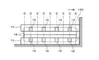
駆動電極15を形成した後、ウエハー10の表面から、図4に示すように、チャネル13の底部又は底部近傍に至る深さで、チャネル13の長さ方向と直交する方向に沿って該チャネル13の全てに亘って複数本のざぐり溝16を平行に研削加工する(ざぐり溝加工工程)。図4(a)はウエハー10の平面図、(b)はウエハー10の正面図である。
After the
隣接するざぐり溝16の間の長さAは、インクジェットヘッドに要求されるチャネル特性(L長)の2倍の長さであり、また、各ざぐり溝16の間は等間隔であって、そのピッチPは、作成されるヘッドチップの長さ(インク吐出方向に沿う長さ)の2倍の長さとなるように、それぞれ位置決めして各ざぐり溝16を加工する。なお、これら2倍の長さとは、それぞれ研削加工時の加工しろを除いた長さである。
The length A between the
ざぐり溝16の幅は、要求されるヘッドチップのL長によって適宜設定される。すなわち、このざぐり溝16の幅を適宜設定することによって、ヘッドチップの長さを共通にしても、L長の異なる様々な特性を有するヘッドチップを作成することができるようになる。
The width of the
また、ざぐり溝16の本数は、ウエハー10からのヘッドチップの取り数によって適宜設定される。
Further, the number of
ざぐり溝16の深さは、チャネル13の底部又は底部近傍に至る深さであればよいが、チャネル13の深さよりも若干深くなる程度とすることが好ましい。このようにざぐり溝16を加工することで、ざぐり溝16の内部に位置するチャネル13の底部の駆動電極15も同時に削り取られるため、得られるヘッドチップの静電容量を下げることができる。
The depth of the
ざぐり溝16の加工は、ウエハー10に溝加工することができるものであれば、加工手段は特に問わないが、チャネル13の溝加工と同様にダイシングソーを用いて行うことが好ましい。ダイシングソーによれば、機械的に高精度な位置決めによる研削加工が可能であり、ざぐり溝16の幅、深さ及び間隔を高精度に設定できる。
The machining of the counterbored
このざぐり溝16を加工する際、同一刃を用いて、ウエハー10の外形端を該ざぐり溝16と平行に切断加工することが好ましい。図4中の符号17は、外形端を切断加工する際の加工しろ、符号10aは、切り離されたウエハー10の端部である。この外形端の切断加工は、ざぐり溝16と同一刃を用いるため、ざぐり溝16の加工と同一ワーク内での加工作業で行うことができ、端部からの位置精度も高精度に確保することができる。
When machining the
ざぐり溝16及び外形端の切断加工の後、ウエハー10の表面に、チャネル13の上部を塞ぐようにカバー基板18を接着する(カバー基板接着工程)。図5は、表面にカバー基板18を接着したウエハー10の側面図である。
After cutting the
カバー基板18には、駆動壁14を構成する圧電材料と同一の基板材料を脱分極して用いると、カバー基板18を加熱接着する時の熱や、インクジェットヘッド完成後の駆動時の発熱の影響によって、熱膨張係数の差に起因する速度分布や駆動特性のばらつきを少なくすることができる。
If the same substrate material as the piezoelectric material constituting the
次に、同様にしてカバー基板18を接着したウエハー10を2組用意し、そのカバー基板18同士を重ね合わせるように積層してエポキシ系接着剤を用いて接着する(積層接着工程)。
Next, two sets of
図6は、カバー基板18同士を接着した状態を示す側面図である。同図に示すように、積層接着時は、上下の各ウエハー10、10を、それぞれのチャネル13が同一方向となるように重ね合わせると共に、上記ざぐり溝加工工程において外形端が切断加工された切断加工面同士を、作業台等の位置決め部材100に突き当てる。この切断加工面は、ざぐり溝16の加工時に同一刃を用いて同一ワーク内の作業によって、ざぐり溝16からの位置も高精度に位置決めされて形成されているため、上下のウエハー10、10の各ざぐり溝16、16の上下方向の位置を容易且つ高精度に合致させて位置決めすることができる。
FIG. 6 is a side view showing a state where the
この突き当てによる位置決めの後、2枚のウエハー10、10をカバー基板18、18と共に切断し、多数のヘッドチップ1Aを切り出す(切断加工工程)。
After positioning by this abutment, the two
図6中の各一点鎖線は、この切断加工時の切断ラインCを示している。この切断ラインCは、チャネル13の長さ方向と直交する方向に沿って平行に位置決めされ、この切断ラインCに沿ってダイシングソーを用いて切断する。
Each dashed-dotted line in FIG. 6 has shown the cutting line C at the time of this cutting process. The cutting line C is positioned in parallel along a direction orthogonal to the length direction of the
隣接する切断ラインC、Cの間隔は、作成されるヘッドチップ1Aのインク吐出方向に沿う長さである。この間隔は、ヘッドチップ1A自体の強度、インクジェットヘッドの組み立て作業性、インクジェットヘッドを外装へ取り付けする際の取り付け作業性等を考慮して、切り出されるヘッドチップ1A、1A・・・が全て同じ最適な長さとなるように決定される。
The interval between the adjacent cutting lines C and C is a length along the ink ejection direction of the
図6に示すように、この隣接する2本の切断ラインC、Cのうちの一方は、ざぐり溝16の上から該ざぐり溝16の長さ方向に沿って、ざぐり溝16の中央を通るように形成され、他方は、隣接するざぐり溝16、16の間で、その中央を通るように形成される。従って、隣接する2本の切断ラインC、Cによって1つのヘッドチップ1Aが切り出される。
As shown in FIG. 6, one of the two adjacent cutting lines C, C passes through the center of the counterbored
図7は、このようにして切り出された1つのヘッドチップ1Aの側面図である。
FIG. 7 is a side view of one
このヘッドチップ1Aは、図示上側のウエハー10に並設された各チャネル13によるチャネル列と、下側のウエハー10に並設された各チャネル13によるチャネル列との2列のチャネル列を有している。ヘッドチップ1Aの前面(図示右側の面)及び後面側(図示左側)に、それぞれ各チャネル13の出口と入口とが配置される。各チャネル13は、入口から出口に亘る長さ方向で大きさと形状がほぼ変わらないストレートタイプとなる。
This
また、ヘッドチップ1Aの後面側には、ウエハー10に加工されたざぐり溝16によって形成された2本のざぐり部19、19を、各チャネル列に沿ってそれぞれ溝状に有している。ヘッドチップ1Aのチャネル特性を決定するL長は、このざぐり部19、19によって、ヘッドチップの長さBに対して所望の長さとなるように短く形成されている。
Further, on the rear surface side of the
切り出された各ヘッドチップ1A、1A…は、ウエハー10の各ざぐり溝16及び各切断ラインCが高精度に位置決めされているため、それぞればらつきのない均質な精度を有している。本発明によれば、このような均質な精度を有し、ヘッドチップの長さBに対して所望のL長を有するヘッドチップ1Aを、一度に多数個作成することが簡単に行えるようになる。
Each of the cut out
このようにして作成されたヘッドチップ1Aは、その前面にノズルが形成されたノズルプレートを接着すると共に、後面にインクマニホールドを接着し、更に各駆動電極15に電圧印加を行うための配線を接続してインクジェットヘッドを完成させる。
The
図8は、インクジェットヘッドの一例を示す断面図である。 FIG. 8 is a cross-sectional view showing an example of an inkjet head.
図中、2はヘッドチップ1Aの前面に接着されたノズルプレートであり、ヘッドチップ1Aの各チャネル13に対応するようにノズル21が形成されている。また、3は配線基板、4は駆動IC(図示せず)から各駆動電極15に電圧印加を行うためのFPCである。
In the figure, reference numeral 2 denotes a nozzle plate bonded to the front surface of the
配線基板3は、非分極のPZTやAlN−BN、AlN等のセラミックス材料からなる1枚の板状の基板によって形成されている。また、低熱膨張のプラスチックやガラス等を用いることもできる。更には、ヘッドチップ1Aに使用されている圧電素子の基板材料と同一の基板材料を脱分極して用いることも好ましい。
The
この構造では、配線基板3とヘッドチップ1Aの接着部分は、ざぐり部19の深さが深くなるほど駆動壁14から離れる。配線基板3として、ヘッドチップ1Aと熱膨張係数が異なる材料を用いる場合、加熱接着時から室温に戻ったときに熱膨張係数の差による応力が発生し、駆動に悪影響を与えるおそれがある。本発明では、ざぐり部19によって駆動壁14を配線基板3との接着部分から離すことができるため、この影響を小さくすることができ、配線基板3としてヘッドチップ1Aと熱膨張係数が異なる材料を使用することを容易にする。
In this structure, the bonding portion between the
配線基板3を構成する材料は1枚板に限らず、薄板状の基板材料を複数枚積層して所望の厚みとなるように形成してもよい。
The material constituting the
この配線基板3は、ヘッドチップ1Aの幅方向と同一の幅を有すると共に、ヘッドチップ1Aのチャネル列方向と直交する方向(図8の上下方向)に延びて大きく張り出している。
The
なお、ヘッドチップ1Aには、各チャネル13内の駆動電極15からヘッドチップ1Aの前面及び上面、下面をそれぞれ経由して、ヘッドチップ1Aの後面に至る引き出し電極150を形成しておく。この引き出し電極150は、蒸着法やスパッタリング法等によって形成することができる。
In the
配線基板3のヘッドチップ1Aとの接着面には、ヘッドチップ1Aから大きく張り出した部分に、ヘッドチップ1Aの引き出し電極150と接続する配線31が形成されており、配線基板3は、この配線31がヘッドチップ1Aに対してそれぞれ位置決めされ、異方導電性フィルム等によって電気的に接続されて接着される。引き出し配線150と配線31との電気的接続方法としては、この他に、導電性粒子を含む異方性導電ペースト、非導電性接着剤で接着する圧接接合、配線31と引き出し電極150の少なくとも一方に半田を使用し、加熱溶融させて接続する方法等、通常の実装技術で使用されている方法を用いることもできる。
On the bonding surface of the
配線基板3のヘッドチップ1Aよりも上方及び下方に露出する配線31には、それぞれFPC4の配線41が、異方導電性フィルム等によって電気的に接続されて接着される。
A
この配線基板3の接着により、ヘッドチップ1Aの各駆動電極15への駆動ICからの電圧印加が可能となると共に、ヘッドチップ1Aの各ざぐり部19、19と凹部32、32とによって、各チャネル13にインクを供給するためのインク共通室5、5が形成される。このインク共通室5、5は、配線基板3の凹部32とヘッドチップ1Aのざぐり部19、19とによって形成されるため、凹部32のみによって形成されるものに比較して大きな容積を確保することができる。
The adhesion of the
この態様では、配線基板3に2本の凹部32、32を形成したので、カバー基板18、18によって2つのインク共通室5、5が隔絶される。従って、各チャネル列に異なる色のインクをそれぞれ供給するように構成することもできる。
In this embodiment, since the two
(第2の実施形態)
第1の実施形態では、積層接着工程において、図6に示すように、それぞれカバー基板18を接着した2組のウエハー10のカバー基板18同士を積層して接着したが、図9に示すように、ウエハー10同士を接着してもよい。この場合も、図6と同様に、外形端が切断加工された切断加工面を位置決め部材100に突き当てて、各組のざぐり溝16、16同士を上下方向で合致させた後、同様に切断加工すればよい。これにより作成されるヘッドチップ1Bは、図10に示すように、第1の実施形態に係るヘッドチップ1Aのカバー基板18とウエハー10の部分が逆の態様となる。
(Second Embodiment)
In the first embodiment, in the lamination bonding step, as shown in FIG. 6, the
(第3の実施形態)
2列のチャネル列を有するヘッドチップを作成する場合、ざぐり溝16の加工は、図11に示すように、チャネル13を溝加工したウエハー10にカバー基板18を接着した後に行うこともできる。図11は、ウエハー10にカバー基板18を接着した後にざぐり溝16を加工した状態を示す側面図である。図4(b)と同一符号は同一構成を示している。
(Third embodiment)
In the case of producing a head chip having two channel rows, the counterbored
この態様では、図12に示すように、2組のウエハー10、10のカバー基板18、18同士を重ね合わせて接着し、図6と同様に、外形端が切断加工された切断加工面を位置決め部材100に突き当てて、各組のざぐり溝16、16同士を上下方向で合致させた後、同様に切断加工してヘッドチップ1Cを切り出せばよい。これにより切り出されたヘッドチップ1Cは、図13に示すように、上下のチャネル列の間に、図7に示すヘッドチップ1Aのようにカバー基板18、18がせり出しておらず、ざぐり溝16、16同士が一体となった大きな1つのざぐり部190が形成される。
In this embodiment, as shown in FIG. 12, the
このヘッドチップ1Cによって図8と同様のインクジェットヘッドを作成する場合、配線基板3にはざぐり部190に対応させて凹部32を1本だけ形成すればよく、これによって1つの大きなインク共通室が形成される。
When an ink jet head similar to that shown in FIG. 8 is formed by using the
(第4の実施形態)
以上の各実施形態では、2列のチャネル列を有するヘッドチップ1A〜1Cを作成したが、チャネル列は2列に限らず、1列のみであってもよい。この場合は、カバー基板接着工程までは第1の実施形態と同一の工程で行うことができる。
(Fourth embodiment)
In each of the embodiments described above, the head chips 1A to 1C having two channel rows are created, but the channel row is not limited to two rows, and may be only one row. In this case, the process up to the cover substrate bonding process can be performed in the same process as in the first embodiment.
その後は、図5に示すカバー基板18を接着した後のウエハー10を、切断加工すればよい。
Thereafter, the
(第5の実施形態)
ざぐり溝16の加工は、チャネル特性に影響する部分に対して行えばよく、必ずしも図4に示すようにウエハー10の一方端から他方端に亘って横断するように形成する必要はなく、例えば図14に示すように、ウエハー10のうちのチャネル13が形成されている領域のみに対して形成し、ウエハー10の各端部10bは削り残すようにしてもよい。
(Fifth embodiment)
The counterbored
図15は、このようにして作成されたヘッドチップ1Dの横断面図である。このヘッドチップ1Dは、ざぐり溝16の加工方法以外は、第1の実施形態と同一の工程によって作成されたものを示している。同図に示すように、ヘッドチップ1Dの両端は、削り残されたウエハーの端部10b、10bによってざぐり部19の両端が開口しないため、ヘッドチップ1Dの両端をインク漏れが生じないように閉塞する等の手段を講じる必要がなくなる。
FIG. 15 is a cross-sectional view of the
なお、本発明において、ヘッドチップ1A〜1Dの各駆動電極15に電圧印加するための配線の接続方法は、配線基板3による方法に何ら限定されず、様々な方法を採用することができる。
In the present invention, the wiring connection method for applying a voltage to each of the
1A〜1D:ヘッドチップ
10:ウエハー
10a、10b:端部
11:基板
12a、12b:分極処理された圧電素子基板
13:チャネル
14:駆動壁
15:駆動電極
150:引き出し電極
16:ざぐり溝
17:加工しろ
18:カバー基板
19、190:ざぐり部
2:ノズルプレート
21:ノズル
3:配線基板
31:配線
32:凹部
4:FPC
41:配線
5:インク共通室
1A to 1D: Head chip 10:
41: Wiring 5: Ink common chamber
Claims (4)
前記ヘッドチップを作成する工程は、
少なくとも表面に圧電素子層を含むウエハーの表面から多数のチャネルを溝加工するチャネル加工工程と、
前記チャネル内に電極を形成する電極形成工程と、
前記電極が形成されたウエハーの表面に、前記チャネルの上部を塞ぐようにカバー基板を接着するカバー基板接着工程と、
前記カバー基板を接着した後の該カバー基板側又は前記ウエハー側から前記チャネルの底部又は底部近傍に至る深さで、前記チャネルと直交する方向に沿って該チャネルの全てに亘って複数本のざぐり溝を、隣接するざぐり溝の間の長さがインクジェットヘッドに要求されるチャネル特性の2倍の長さとなるように加工するざぐり溝加工工程と、
前記ざぐり溝が加工されたウエハーを2組用意し、前記ざぐり溝が加工された側同士を該ざぐり溝同士が重なるように積層させて接着する積層接着工程と、
前記ざぐり溝が加工された側同士を重ね合わせて接着したウエハーを、前記チャネルと直交する方向の切断ラインに沿って切断して、2列のチャネル列を有する所定サイズのヘッドチップを多数個切り出す切断工程とを有し、
前記切断工程では、1つのヘッドチップを切り出すための2本の切断ラインのうちの一方を、前記ざぐり溝の上から該ざぐり溝に沿って形成し、他方を、隣接する前記ざぐり溝の間に形成することを特徴とするインクジェットヘッドの製造方法。 A drive chip and a channel made of piezoelectric elements are alternately arranged side by side, and an outlet and an inlet of the channel are arranged to face each other, and an electrode for applying a voltage to the drive wall is formed. A method of manufacturing an ink jet head, wherein a voltage is applied to the electrode to shear the drive wall, and ink in the channel is ejected from a nozzle.
The step of creating the head chip includes:
A channel processing step of grooving a number of channels from the surface of the wafer including at least the surface of the piezoelectric element layer;
Forming an electrode in the channel; and
A cover substrate adhering step of adhering a cover substrate to the surface of the wafer on which the electrode is formed so as to close the upper portion of the channel;
A plurality of counterbores across all of the channels along a direction perpendicular to the channel at a depth from the cover substrate side or the wafer side after the cover substrate is bonded to the bottom or near the bottom of the channel. A counterbored groove processing step in which the groove is processed so that the length between adjacent counterbored grooves is twice as long as the channel characteristics required for the inkjet head;
A laminate bonding step of preparing two sets of wafers processed with the counterbored grooves, and laminating and bonding the side of the counterbored grooves so that the counterbored grooves overlap each other;
The wafer having the counterbored grooves formed on each other and bonded to each other is cut along a cutting line in a direction perpendicular to the channel to cut out a large number of head chips of a predetermined size having two channel rows. Cutting process,
In the cutting step, one of two cutting lines for cutting out one head chip is formed along the counterbored groove from above the counterbored groove, and the other is disposed between the adjacent counterbored grooves. A method of manufacturing an ink jet head, comprising: forming an ink jet head.
Priority Applications (1)
| Application Number | Priority Date | Filing Date | Title |
|---|---|---|---|
| JP2006127015A JP4876701B2 (en) | 2006-04-28 | 2006-04-28 | Inkjet head manufacturing method |
Applications Claiming Priority (1)
| Application Number | Priority Date | Filing Date | Title |
|---|---|---|---|
| JP2006127015A JP4876701B2 (en) | 2006-04-28 | 2006-04-28 | Inkjet head manufacturing method |
Publications (3)
| Publication Number | Publication Date |
|---|---|
| JP2007296758A JP2007296758A (en) | 2007-11-15 |
| JP2007296758A5 JP2007296758A5 (en) | 2009-06-04 |
| JP4876701B2 true JP4876701B2 (en) | 2012-02-15 |
Family
ID=38766661
Family Applications (1)
| Application Number | Title | Priority Date | Filing Date |
|---|---|---|---|
| JP2006127015A Expired - Fee Related JP4876701B2 (en) | 2006-04-28 | 2006-04-28 | Inkjet head manufacturing method |
Country Status (1)
| Country | Link |
|---|---|
| JP (1) | JP4876701B2 (en) |
Families Citing this family (1)
| Publication number | Priority date | Publication date | Assignee | Title |
|---|---|---|---|---|
| JP5846050B2 (en) * | 2012-06-08 | 2016-01-20 | コニカミノルタ株式会社 | Head chip manufacturing method and inkjet head manufacturing method |
Family Cites Families (4)
| Publication number | Priority date | Publication date | Assignee | Title |
|---|---|---|---|---|
| JP3662480B2 (en) * | 2000-07-12 | 2005-06-22 | シャープ株式会社 | Ink ejecting apparatus and manufacturing method thereof |
| JP4260472B2 (en) * | 2002-08-23 | 2009-04-30 | シャープ株式会社 | Ink jet head and manufacturing method thereof |
| JP2004098345A (en) * | 2002-09-05 | 2004-04-02 | Sharp Corp | Inkjet head unit structure and process for producing inkjet head |
| JP4590934B2 (en) * | 2003-09-05 | 2010-12-01 | コニカミノルタホールディングス株式会社 | Inkjet head manufacturing method |
-
2006
- 2006-04-28 JP JP2006127015A patent/JP4876701B2/en not_active Expired - Fee Related
Also Published As
| Publication number | Publication date |
|---|---|
| JP2007296758A (en) | 2007-11-15 |
Similar Documents
| Publication | Publication Date | Title |
|---|---|---|
| JP4357600B2 (en) | Fluid ejection device | |
| JP2006082396A (en) | Ink-jet head | |
| JP4984661B2 (en) | Inkjet head manufacturing method and inkjet head | |
| WO1996000151A1 (en) | Piezoelectric actuator for ink jet head and method of manufacturing same | |
| JP6103209B2 (en) | Method for manufacturing liquid jet head | |
| JP5555570B2 (en) | Ink jet head and manufacturing method thereof | |
| JP4876701B2 (en) | Inkjet head manufacturing method | |
| JP6140941B2 (en) | Liquid discharge head and manufacturing method thereof | |
| JP4613704B2 (en) | Inkjet head manufacturing method | |
| JP4222218B2 (en) | Nozzle plate, nozzle plate manufacturing method, and inkjet head manufacturing method | |
| JP3680519B2 (en) | Inkjet head manufacturing method | |
| JP4590934B2 (en) | Inkjet head manufacturing method | |
| JP2007076062A (en) | Method for manufacturing inkjet head | |
| JP3298755B2 (en) | Method of manufacturing inkjet head | |
| JP2007320187A (en) | Method of manufacturing inkjet head, and inkjet head | |
| JP5846050B2 (en) | Head chip manufacturing method and inkjet head manufacturing method | |
| JP4321233B2 (en) | Inkjet head manufacturing method | |
| JP4631343B2 (en) | Ink jet head and manufacturing method thereof | |
| JPH1191114A (en) | Production of nozzle plate for ink jet recording head | |
| JP2004148597A (en) | Ink jet head and its manufacturing process | |
| JP2002052712A (en) | Ink ejector | |
| JP2007168097A (en) | Method of manufacturing inkjet head | |
| JP2000211135A (en) | Ink-jet printing head and production thereof | |
| JP2006035453A (en) | Manufacturing method for inkjet head | |
| JP2002019112A (en) | Ink jet device and method of making the same |
Legal Events
| Date | Code | Title | Description |
|---|---|---|---|
| A521 | Written amendment |
Free format text: JAPANESE INTERMEDIATE CODE: A523 Effective date: 20090417 |
|
| A621 | Written request for application examination |
Free format text: JAPANESE INTERMEDIATE CODE: A621 Effective date: 20090417 |
|
| A977 | Report on retrieval |
Free format text: JAPANESE INTERMEDIATE CODE: A971007 Effective date: 20110623 |
|
| A131 | Notification of reasons for refusal |
Free format text: JAPANESE INTERMEDIATE CODE: A131 Effective date: 20110705 |
|
| A521 | Written amendment |
Free format text: JAPANESE INTERMEDIATE CODE: A523 Effective date: 20110803 |
|
| TRDD | Decision of grant or rejection written | ||
| A01 | Written decision to grant a patent or to grant a registration (utility model) |
Free format text: JAPANESE INTERMEDIATE CODE: A01 Effective date: 20111101 |
|
| A01 | Written decision to grant a patent or to grant a registration (utility model) |
Free format text: JAPANESE INTERMEDIATE CODE: A01 |
|
| A61 | First payment of annual fees (during grant procedure) |
Free format text: JAPANESE INTERMEDIATE CODE: A61 Effective date: 20111114 |
|
| R150 | Certificate of patent or registration of utility model |
Free format text: JAPANESE INTERMEDIATE CODE: R150 Ref document number: 4876701 Country of ref document: JP Free format text: JAPANESE INTERMEDIATE CODE: R150 |
|
| FPAY | Renewal fee payment (event date is renewal date of database) |
Free format text: PAYMENT UNTIL: 20141209 Year of fee payment: 3 |
|
| S531 | Written request for registration of change of domicile |
Free format text: JAPANESE INTERMEDIATE CODE: R313531 |
|
| S533 | Written request for registration of change of name |
Free format text: JAPANESE INTERMEDIATE CODE: R313533 |
|
| R350 | Written notification of registration of transfer |
Free format text: JAPANESE INTERMEDIATE CODE: R350 |
|
| LAPS | Cancellation because of no payment of annual fees |