JP4874207B2 - Circuit simulation method, circuit simulation apparatus, and program - Google Patents
Circuit simulation method, circuit simulation apparatus, and program Download PDFInfo
- Publication number
- JP4874207B2 JP4874207B2 JP2007258117A JP2007258117A JP4874207B2 JP 4874207 B2 JP4874207 B2 JP 4874207B2 JP 2007258117 A JP2007258117 A JP 2007258117A JP 2007258117 A JP2007258117 A JP 2007258117A JP 4874207 B2 JP4874207 B2 JP 4874207B2
- Authority
- JP
- Japan
- Prior art keywords
- stress
- active region
- distance
- modulation amount
- mos transistor
- Prior art date
- Legal status (The legal status is an assumption and is not a legal conclusion. Google has not performed a legal analysis and makes no representation as to the accuracy of the status listed.)
- Expired - Fee Related
Links
Images


Classifications
-
- G—PHYSICS
- G06—COMPUTING; CALCULATING OR COUNTING
- G06F—ELECTRIC DIGITAL DATA PROCESSING
- G06F30/00—Computer-aided design [CAD]
- G06F30/30—Circuit design
- G06F30/36—Circuit design at the analogue level
- G06F30/367—Design verification, e.g. using simulation, simulation program with integrated circuit emphasis [SPICE], direct methods or relaxation methods
Description
本発明は、回路シミュレーション方法、回路シミュレーション装置、及び回路シミュレーション用プログラムに関し、特に、MOSトランジスタに印加される応力を考慮して回路シミュレーションを行う技術に関する。 The present invention relates to a circuit simulation method, a circuit simulation device, and a circuit simulation program, and more particularly to a technique for performing circuit simulation in consideration of stress applied to a MOS transistor.
半導体集積回路の開発においては、回路シミュレーションが重要な役割を果たしている。回路シミュレーションによって設計した半導体集積回路の動作検証を行い、当該半導体集積回路が設計仕様を満足するか確かめることにより、所望の機能や性能を有する半導体集積回路を開発することができる。 Circuit simulation plays an important role in the development of semiconductor integrated circuits. By verifying the operation of a semiconductor integrated circuit designed by circuit simulation and confirming whether the semiconductor integrated circuit satisfies the design specifications, a semiconductor integrated circuit having a desired function and performance can be developed.
伝統的な回路シミュレーションの手順は、概略的には、以下の通りである:まず、MOSトランジスタのレイアウト寸法(例えば、ゲート長L、ゲート幅Wその他)が様々に異なる各MOSトランジスタの特性を実測する。次に実測によって得られた測定データから、各MOSトランジスタの特性を表すトランジスタモデルパラメータを抽出する。回路シミュレーションは、そのトランジスタモデルパラメータを用いて行われる。回路シミュレータとしては、SPICE(Simulation Program with Integrated Circuit Emphasis)が標準的に使用される。この場合、SPICEの形式に即したトランジスタモデル(例えば、BSIM3(Berkley Short Channel IGFET Model 3)やBSIM4)で定義されるトランジスタモデルパラメータが抽出され、回路シミュレーションに使用される。回路シミュレーションの精度の向上は、半導体集積回路の動作検証を適切に行う上で重要である。 The procedure of traditional circuit simulation is roughly as follows: First, the characteristics of MOS transistors having different layout dimensions (eg, gate length L, gate width W, etc.) of MOS transistors are measured. To do. Next, transistor model parameters representing the characteristics of each MOS transistor are extracted from measurement data obtained by actual measurement. The circuit simulation is performed using the transistor model parameters. As a circuit simulator, SPICE (Simulation Program with Integrated Circuit Emphasis) is typically used. In this case, transistor model parameters defined by a transistor model (for example, BSIM3 (Berkley Short Channel IGFET Model 3) or BSIM4) conforming to the SPICE format are extracted and used for circuit simulation. Improving the accuracy of circuit simulation is important for proper verification of the operation of a semiconductor integrated circuit.
近年、回路シミュレーションの精度を落とす要因の一つとして着目されているのが、MOSトランジスタに作用する応力の影響である。半導体集積回路のプロセスの微細化により、MOSトランジスタに作用する応力の影響、特に、応力によるチャネル移動度や閾値電圧の変動の影響が増大している。微細化された半導体集積回路では、MOSトランジスタに作用する応力を回路シミュレーションにおいて考慮することが望ましい。 In recent years, attention has been focused on the influence of stress acting on a MOS transistor as one of the factors that reduce the accuracy of circuit simulation. With the miniaturization of the process of the semiconductor integrated circuit, the influence of stress acting on the MOS transistor, in particular, the influence of fluctuations in channel mobility and threshold voltage due to the stress is increasing. In a miniaturized semiconductor integrated circuit, it is desirable to consider the stress acting on the MOS transistor in the circuit simulation.
MOSトランジスタに作用する応力を考慮して回路シミュレーションを行う技術は、例えば、特開2004−86546号公報に開示されている。この公報に記載の技術では、概略的には、下記の手順で回路シミュレーションが行われる(段落[0050]〜[0052]等)。まず、応力のパラメータを基にパラメータ抽出を行って複数のモデルパラメータが生成される。更に、その複数のモデルパラメータのうちから、トランジスタサイズに応じて最適なモデルパラメータが選択される。選択されたモデルパラメータを用いて回路シミュレーションが行われる。素子分離用絶縁膜からの応力がMOSトランジスタの特性に与える影響が大きいことを指摘している(段落[0038]、[0039]等)。応力の指標として使用する事項としては、素子分離用絶縁膜の、活性領域のゲート長方向に位置する両側の分離幅、及び活性領域のゲート幅方向に位置する両側の分離幅が挙げられている(段落[0080])。 A technique for performing circuit simulation in consideration of the stress acting on the MOS transistor is disclosed in, for example, Japanese Patent Application Laid-Open No. 2004-86546. In the technique described in this publication, circuit simulation is generally performed according to the following procedure (paragraphs [0050] to [0052] and the like). First, a plurality of model parameters are generated by performing parameter extraction based on stress parameters. Furthermore, an optimal model parameter is selected from the plurality of model parameters according to the transistor size. Circuit simulation is performed using the selected model parameters. It is pointed out that the stress from the element isolation insulating film has a great influence on the characteristics of the MOS transistor (paragraphs [0038], [0039], etc.). The matters used as the index of stress include the isolation width on both sides of the element isolation insulating film positioned in the gate length direction of the active region and the isolation width on both sides positioned in the gate width direction of the active region. (Paragraph [0080]).
また、特開2006−178907号公報は、ゲート幅方向における隣接活性領域までの距離を応力の指標として用いる技術を開示している。特開2006−178907号公報は、ゲート幅方向における隣接活性領域までの距離から補正近似式によってトランジスタモデルパラメータを補正する技術を開示している。 Japanese Patent Laid-Open No. 2006-178907 discloses a technique that uses a distance to an adjacent active region in the gate width direction as an index of stress. Japanese Patent Application Laid-Open No. 2006-178907 discloses a technique for correcting a transistor model parameter from a distance to an adjacent active region in the gate width direction using a correction approximate expression.
更に、特開2004−327463号公報は、活性領域の長さと幅から、モデル式を用いてチャネル領域に印加される応力を算出し、算出された応力からキャリア移動度を計算し、そのキャリア移動度からドレイン電流を算出する技術を開示している。
しかしながら、発明者の検討によれば、上述の3つの技術では、MOSトランジスタのチャネル領域に印加される応力を適切に考慮することができず、精度が高い回路シミュレーションを行うことができないという課題がある。 However, according to the inventor's study, the above-described three techniques cannot properly take into account the stress applied to the channel region of the MOS transistor, and cannot perform highly accurate circuit simulation. is there.
上記の課題を解決するために、本発明は、以下に述べられる手段を採用する。その手段を構成する技術的事項の記述には、[特許請求の範囲]の記載と[発明を実施するための最良の形態]の記載との対応関係を明らかにするために、[発明を実施するための最良の形態]で使用される番号・符号が付記されている。但し、付記された番号・符号は、[特許請求の範囲]に記載されている発明の技術的範囲を限定的に解釈するために用いてはならない。 In order to solve the above problems, the present invention employs the means described below. In the description of technical matters constituting the means, in order to clarify the correspondence between the description of [Claims] and the description of [Best Mode for Carrying Out the Invention] No./symbol used in [Best Mode for Doing]. However, the appended numbers and symbols should not be used to limit the technical scope of the invention described in [Claims].
一の観点において、本発明の回路シミュレーション方法は、図形情報生成手段(3)と、パラメータ変調量計算手段(3)と、回路シミュレーション手段(4)とを備える回路シミュレーション装置によって回路シミュレーションを行う方法である。当該回路シミュレーション方法は、
(a)前記図形情報生成手段(3)が、対象MOSトランジスタ(30)のレイアウト寸法を示す図形情報(19)を生成するステップと、
(b)前記パラメータ変調量計算手段(3)が、前記図形情報(19)に基づいてパラメータ変調量(20)を計算するステップと、
(c)前記回路シミュレーション手段(4)が、与えられたトランジスタモデルパラメータ(17)を前記パラメータ変調量(20)によって修正し、修正されたトランジスタモデルパラメータ(17)を用いて前記対象MOSトランジスタ(30)を含む回路の回路シミュレーションを行うステップ
とを具備している。前記パラメータ変調量の計算は、前記図形情報に基づいて前記パラメータ変調量を算出する演算式によって行われる。前記演算式は、MOSトランジスタのチャネル領域に作用する応力を表す応力モデル式を含んでいる。前記応力モデル式は、前記応力の大きさが、前記MOSトランジスタの前記チャネル領域が形成されている活性領域からそれに隣接する活性領域までの距離である隣接距離の増加に対して単調に減少し、且つ、前記隣接距離が無限に大きい場合に一定値に収束し、且つ、前記応力の前記隣接距離に対する微分係数の大きさが単調に減少し、且つ、前記微分係数が前記隣接距離が無限に大きい場合に0に収束するように決定されている。
In one aspect, the circuit simulation method of the present invention is a method for performing circuit simulation by a circuit simulation apparatus comprising graphic information generation means (3), parameter modulation amount calculation means (3), and circuit simulation means (4). It is. The circuit simulation method is as follows:
(A) the graphic information generating means (3) generating graphic information (19) indicating a layout dimension of the target MOS transistor (30);
(B) the parameter modulation amount calculating means (3) calculating a parameter modulation amount (20) based on the graphic information (19);
(C) The circuit simulation means (4) modifies the given transistor model parameter (17) by the parameter modulation amount (20), and uses the modified transistor model parameter (17) to generate the target MOS transistor ( And 30) performing a circuit simulation of the circuit including the above. The parameter modulation amount is calculated by an arithmetic expression for calculating the parameter modulation amount based on the graphic information. The arithmetic expression includes a stress model expression representing the stress acting on the channel region of the MOS transistor. In the stress model formula, the magnitude of the stress monotonously decreases with an increase in adjacent distance, which is a distance from an active region in which the channel region of the MOS transistor is formed to an active region adjacent thereto, And when the adjacent distance is infinitely large, it converges to a constant value, the magnitude of the differential coefficient of the stress with respect to the adjacent distance monotonously decreases, and the differential coefficient has an infinitely large adjacent distance. In this case, it is determined to converge to 0.
他の観点において、本発明の回路シミュレーション装置は、対象MOSトランジスタ(30)のレイアウト寸法を示す図形情報(19)を生成する図形情報生成手段(3)と、前記図形情報(19)に基づいてパラメータ変調量(20)を計算するパラメータ変調量計算手段(3)と、与えられたトランジスタモデルパラメータ(17)を前記パラメータ変調量(20)によって修正し、修正されたトランジスタモデルパラメータを用いて前記対象MOSトランジスタ(30)を含む回路の回路シミュレーションを行う回路シミュレーション手段(4)とを具備する。前記パラメータ変調量の計算は、前記図形情報に基づいて前記パラメータ変調量を算出する演算式によって行われる。前記演算式は、MOSトランジスタのチャネル領域に作用する応力を表す応力モデル式を含んでいる。前記応力モデル式は、前記応力の大きさが、前記MOSトランジスタの前記チャネル領域が形成されている活性領域からそれに隣接する活性領域までの距離である隣接距離の増加に対して単調に減少し、且つ、前記隣接距離が無限に大きい場合に一定値に収束し、且つ、前記応力の前記隣接距離に対する微分係数の大きさが単調に減少し、且つ、前記微分係数が前記隣接距離が無限に大きい場合に0に収束するように決定されている。 In another aspect, the circuit simulation apparatus of the present invention is based on the graphic information generating means (3) for generating graphic information (19) indicating the layout dimension of the target MOS transistor (30) and the graphic information (19). The parameter modulation amount calculation means (3) for calculating the parameter modulation amount (20), the given transistor model parameter (17) is modified by the parameter modulation amount (20), and the modified transistor model parameter is used to Circuit simulation means (4) for performing circuit simulation of a circuit including the target MOS transistor (30). The parameter modulation amount is calculated by an arithmetic expression for calculating the parameter modulation amount based on the graphic information. The arithmetic expression includes a stress model expression representing the stress acting on the channel region of the MOS transistor. In the stress model formula, the magnitude of the stress monotonously decreases with an increase in adjacent distance, which is a distance from an active region in which the channel region of the MOS transistor is formed to an active region adjacent thereto, And when the adjacent distance is infinitely large, it converges to a constant value, the magnitude of the differential coefficient of the stress with respect to the adjacent distance monotonously decreases, and the differential coefficient has an infinitely large adjacent distance. In this case, it is determined to converge to 0.
更に他の観点において、本発明のプログラムは、
(a)対象MOSトランジスタ(30)のレイアウト寸法を示す図形情報(19)を生成するステップと、
(b)回路シミュレーションのために回路シミュレータに与えられるトランジスタモデルパラメータの修正量を示すパラメータ変調量(20)を前記図形情報(19)に基づいて計算するステップとをコンピュータに実行させるプログラムである。前記パラメータ変調量の計算は、前記図形情報に基づいて前記パラメータ変調量を算出する演算式によって行われ、前記演算式は、MOSトランジスタのチャネル領域に作用する応力を表す応力モデル式を含んでいる。前記応力モデル式は、前記応力の大きさが、前記MOSトランジスタの前記チャネル領域が形成されている活性領域からそれに隣接する活性領域までの距離である隣接距離の増加に対して単調に減少し、且つ、前記隣接距離が無限に大きい場合に一定値に収束し、且つ、前記応力の前記隣接距離に対する微分係数の大きさが単調に減少し、且つ、前記微分係数が前記隣接距離が無限に大きい場合に0に収束するように決定されている。
In still another aspect, the program of the present invention is
(A) generating graphic information (19) indicating a layout dimension of the target MOS transistor (30);
(B) A program for causing a computer to execute a step of calculating, based on the graphic information (19), a parameter modulation amount (20) indicating a correction amount of a transistor model parameter given to a circuit simulator for circuit simulation. The calculation of the parameter modulation amount is performed by an arithmetic expression for calculating the parameter modulation amount based on the graphic information, and the arithmetic expression includes a stress model expression representing a stress acting on the channel region of the MOS transistor. . In the stress model formula, the magnitude of the stress monotonously decreases with an increase in adjacent distance, which is a distance from an active region in which the channel region of the MOS transistor is formed to an active region adjacent thereto, And when the adjacent distance is infinitely large, it converges to a constant value, the magnitude of the differential coefficient of the stress with respect to the adjacent distance monotonously decreases, and the differential coefficient has an infinitely large adjacent distance. In this case, it is determined to converge to 0.
本発明によれば、MOSトランジスタのチャネル領域に印加される応力を適切に考慮し、精度が高い回路シミュレーションを行うことができる。 According to the present invention, it is possible to perform highly accurate circuit simulation by appropriately considering the stress applied to the channel region of the MOS transistor.
1.本実施形態の回路シミュレーション技術の概略
以下では、まず、本発明の一実施形態に係る回路シミュレーション技術の概略について、図1を参照しながら説明する。
1. Outline of Circuit Simulation Technology of Present Embodiment First, an outline of a circuit simulation technology according to an embodiment of the present invention will be described with reference to FIG.
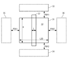
図1は、MOSトランジスタのレイアウトの一例を示す図である。図1において、符号30は、回路シミュレーションの対象のMOSトランジスタを示している。また、符号31は、MOSトランジスタ30の活性領域を示しており、符号32は、MOSトランジスタ30のゲートを示している。ゲート32は、活性領域31を横断するように設けられている。活性領域31のうち、ゲート32の直下に位置する部分が、MOSトランジスタ30のチャネル領域として機能する。活性領域31を取り囲むように、活性領域33〜36が設けられている。活性領域33、34は、活性領域31にゲート幅方向に隣接する活性領域であり、活性領域35、36は、活性領域31にゲート長方向に隣接する活性領域である。活性領域31と活性領域33〜36とは、STI(shallow trench isolation)絶縁膜によって分離されている。図1において、記号LはMOSトランジスタ30のゲート長を示しており、記号WはMOSトランジスタ30のゲート幅を示しており、更に、記号LODは活性領域31のゲート長方向における長さを示している。また、記号PDX1、PDX2は、それぞれ、活性領域31からそれにゲート長方向に隣接する活性領域(即ち、活性領域35、36)までの距離を示しており、記号PDY1、PDY2は、活性領域31からそれにゲート幅方向に隣接する活性領域(即ち、活性領域33、34)までの距離を示している。
FIG. 1 is a diagram illustrating an example of a layout of a MOS transistor. In FIG. 1,
本実施形態の回路シミュレーション技術は、概略的には、下記の通りである。まず、各MOSトランジスタのレイアウト寸法(即ち、L、W、LOD、PDX1、PDX2、PDY1、及びPDY2)に基づいてパラメータ変調量が算出される。ここで、パラメータ変調量とは、回路シミュレーションで使用されるトランジスタモデルパラメータを修正する場合において、その修正量を表す数値である。パラメータ変調量の算出に使用される演算式には、MOSトランジスタの活性領域に作用する応力を表す応力モデル式が含まれており、従って、パラメータ変調量は、活性領域に作用する応力に応じて算出されることになる。算出されたパラメータ変調量を用いてトランジスタモデルパラメータが修正され、修正されたトランジスタモデルパラメータを用いて回路シミュレーションが行われる。 The circuit simulation technique of this embodiment is schematically as follows. First, parameter modulation amounts are calculated based on the layout dimensions of each MOS transistor (that is, L, W, LOD, PDX1, PDX2, PDY1, and PDY2). Here, the parameter modulation amount is a numerical value representing the amount of correction when the transistor model parameter used in the circuit simulation is corrected. The calculation formula used to calculate the parameter modulation amount includes a stress model equation that represents the stress acting on the active region of the MOS transistor. Therefore, the parameter modulation amount depends on the stress acting on the active region. Will be calculated. The transistor model parameter is corrected using the calculated parameter modulation amount, and a circuit simulation is performed using the corrected transistor model parameter.
例えば、SPICEで使用されるトランジスタモデルのトランジスタモデルパラメータU0、VTH0を応力に応じて修正する場合について具体的に説明する。当業者に広く知られているように、U0は、チャネル領域における移動度に対応するパラメータであり、VTH0は、MOSトランジスタの閾値電圧に対応するパラメータである。この場合、パラメータ変調量とは、修正量Δμ、Δν、又は、これらに1対1に対応する数値を意味している。ここで、Δμ、Δνは、トランジスタモデルパラメータU0、VTH0の修正後の値をμ、νとした場合に
Δμ=μ−U0,
Δν=ν−VTH0,
で定義される数値である。「U0」、「VTH0」は、あくまでトランジスタモデルパラメータであり、実測によって得られるチャネル領域の移動度や、MOSトランジスタの閾値電圧とは異なり得ることに留意されたい。電気特性としてのチャネル領域の移動度及び閾値電圧Vtとの混同を避けるため、本明細書では、トランジスタモデルパラメータの一つとしての「U0」は、μ0と記載し、トランジスタモデルパラメータの一つとしての「VTH0」は、ν0と記載する。このような表記によれば、修正量Δμ、Δνは、
Δμ=μ−μ0,
Δν=ν−ν0,
として定義されることになる。
For example, the case where the transistor model parameters U0 and VTH0 of the transistor model used in SPICE are corrected according to the stress will be specifically described. As is widely known to those skilled in the art, U0 is a parameter corresponding to mobility in the channel region, and VTH0 is a parameter corresponding to the threshold voltage of the MOS transistor. In this case, the parameter modulation amount means a correction amount Δμ, Δν, or a numerical value corresponding to the correction amount Δμ, Δν. Here, Δμ and Δν are Δμ = μ−U0 when the corrected values of the transistor model parameters U0 and VTH0 are μ and ν.
Δν = ν−VTH0,
It is a numerical value defined by. It should be noted that “U0” and “VTH0” are transistor model parameters to the last, and may differ from the mobility of the channel region obtained by actual measurement and the threshold voltage of the MOS transistor. In order to avoid confusion between the mobility of the channel region and the threshold voltage Vt as electrical characteristics, in this specification, “U0” as one of the transistor model parameters is described as μ0, and is one of the transistor model parameters. “VTH0” is described as ν0. According to such a notation, the correction amounts Δμ and Δν are
Δμ = μ−μ0,
Δν = ν−ν0,
Will be defined as
本実施形態では、トランジスタモデルパラメータμ0(U0)のパラメータ変調量MULU0としては、修正量Δμではなく、下記式で定義される値が使用される:
MULU0=1+Δμ/μ0.
一方、トランジスタモデルパラメータν0(VTH0)のパラメータ変調量DELVT0としては、修正量Δνがそのまま使用される。即ち、
DELVT0=Δν,
である。
In this embodiment, as the parameter modulation amount MULU0 of the transistor model parameter μ0 (U0), a value defined by the following equation is used instead of the correction amount Δμ:
MULU0 = 1 + Δμ / μ0.
On the other hand, the correction amount Δν is used as it is as the parameter modulation amount DELVT0 of the transistor model parameter ν0 (VTH0). That is,
DELVT0 = Δν,
It is.
算出されたパラメータ変調量MULU0、DELVT0は、SPICEに与えられる。SPICEでは、パラメータ変調量MULU0、DELVT0だけトランジスタモデルパラメータU0、VTH0が修正され、修正後のトランジスタモデルパラメータを用いて回路シミュレーションが行われる。 The calculated parameter modulation amounts MULU0 and DELVT0 are given to SPICE. In SPICE, the transistor model parameters U0 and VTH0 are corrected by parameter modulation amounts MULU0 and DELVT0, and circuit simulation is performed using the corrected transistor model parameters.
以下では、SPICEを用いて回路シミュレーションを行い、且つ、トランジスタモデルパラメータU0、VTH0を応力に応じて修正する場合を例に挙げて、本実施形態の回路シミュレーション技術を詳細に説明する。ただし、他のトランジスタモデルパラメータを応力に応じて修正することも可能であることに留意されたい。 In the following, the circuit simulation technique of this embodiment will be described in detail by taking as an example a case where a circuit simulation is performed using SPICE and the transistor model parameters U0 and VTH0 are corrected according to stress. However, it should be noted that other transistor model parameters can be modified depending on the stress.
2.回路シミュレーションの実装
図2は、本実施形態の回路シミュレーション技術の実装形態の一例を示す図である。本実施形態では、回路図エディタ1、レイアウトエディタ2、LVS(Layout Versus Schematic)ツール3、回路シミュレータ4、及びソルバー5によって、回路設計及び回路シミュレーションが行われる。
2. Implementation of Circuit Simulation FIG. 2 is a diagram illustrating an example of an implementation form of the circuit simulation technique of the present embodiment. In the present embodiment, circuit design and circuit simulation are performed by a circuit diagram editor 1, a layout editor 2, an LVS (Layout Versus Schematic)
回路図エディタ1は、ネットリスト11を生成するために使用されるソフトウェアである。回路図エディタ1によって生成されたネットリスト11は、適宜の記憶装置に保存されてレイアウトエディタ2に引き渡される。本実施形態では、ネットリスト11は、SPICEに対応した形で生成される。
The circuit diagram editor 1 is software used to generate the
レイアウトエディタ2は、ネットリスト11から回路のレイアウトを示すレイアウトデータ12を生成するために使用されるソフトウェアである。生成されたレイアウトデータ12は、適宜の記憶装置に保存されてLVSツール3に引き渡される。
The layout editor 2 is software used to generate
LVSツール3は、レイアウトデータ12から抽出されたネットリストと回路図エディタ1によって生成されたネットリスト11とを比較して、両者が一致しているかどうかを調べ、不一致箇所があれば、レイアウトデータ12を修正するツールである。
The
本実施形態では、LVSツール3は、レイアウトデータ12から各MOSトランジスタのパラメータ変調量を算出するためにも使用される。パラメータ変調量の算出は、必要な演算式をLVSツール3のルールファイルに記述することによって行われる。
In the present embodiment, the
図3は、LVSツール3がパラメータ変調量を算出する手順を示す機能ブロック図である。LVSツール3は、レイアウトデータ12から各MOSトランジスタのレイアウト寸法(即ち、L、W、LOD、PDX1、PDX2、PDY1、及びPDY2)を抽出し、抽出したレイアウト寸法を図形情報19として記憶装置に格納する(ステップS01)。
FIG. 3 is a functional block diagram showing a procedure by which the
更にLVSツール3は、図形情報19に記述されたレイアウト寸法からパラメータ変調量を算出する(ステップS02)。本実施形態では、トランジスタモデルパラメータU0、VTH0のパラメータ変調量MULU0、及びDELVT0が算出される。図3では、パラメータ変調量が、符号20としてまとめて表記されている。
Further, the
パラメータ変調量20の算出に使用される演算式には、MOSトランジスタの活性領域に作用する応力を表す応力モデル式と、パラメータ変調量を算出する関数式とが含まれている。LVSツール3のルールファイルには、この応力モデル式と関数式が記述されている。LVSツール3のルールファイルに記述された応力モデル式には、パラメータが未定のまま残されている。このパラメータは、実際に適用される応力モデル式を最終的に決定するためのパラメータであり、以下において「ストレスモデルパラメータ」と呼ばれる。また、パラメータ変調量を算出する関数式にも、それに含まれるパラメータが未定のまま残されている。このパラメータは、応力がパラメータ変調量に寄与する程度を表しており、以下では、「感度パラメータ」と呼ばれる。ストレスモデルパラメータと感度パラメータとを適切に決定することは、MOSトランジスタのチャネル領域に作用する応力を精度よく算出し、更に、応力がパラメータ変調量に及ぼす影響を的確に考慮するために重要である。ストレスモデルパラメータと感度パラメータについては、後に詳細に説明する。
The arithmetic expressions used for calculating the
応力モデル式とパラメータ変調量を算出する関数式を使用する際には、ストレスモデルパラメータファイル15が参照される。ストレスモデルパラメータファイル15には、予めソルバー5によって抽出されたストレスモデルパラメータと感度パラメータとが記述されている。ストレスモデルパラメータファイル15に記述されたストレスモデルパラメータと感度パラメータとによって実際に適用される応力モデル式及び関数式を決定した後、その応力モデル式及び関数式を含む様々な演算式を用いてパラメータ変調量20が算出される。
When using the stress model formula and the function formula for calculating the parameter modulation amount, the stress
更に、LVSツール3は、算出されたパラメータ変調量20をネットリスト11に追加して変調後ネットリスト16を生成する(ステップS03)。生成された変調後ネットリスト16は、適宜の記憶装置に記憶される。
Furthermore, the
図2を再度に参照して、回路シミュレータ4は、LVSツール3によって生成された変調後ネットリスト16と、事前に抽出されたトランジスタモデルパラメータ17とを用いて回路シミュレーションを行うソフトウェアである。回路シミュレータ4は、変調後ネットリスト16に記述されたパラメータ変調量20に応じてトランジスタモデルパラメータ17を修正し、修正されたトランジスタモデルパラメータを用いて回路シミュレーションを行う。回路シミュレーションの結果は、出力結果18として出力される。本実施形態では、回路シミュレータ4としてはSPICEが使用され、トランジスタモデルパラメータ17は、SPICEに対応した形式で用意される。当業者に広く知られているように、トランジスタモデルパラメータ17は、特定のMOSトランジスタの特性から抽出される。トランジスタモデルパラメータ17の抽出に使用されたMOSトランジスタのレイアウトパターンを、以下では、「SPICE抽出パターン」と呼ぶ。
Referring to FIG. 2 again, the circuit simulator 4 is software that performs circuit simulation using the
ソルバー5は、上述のストレスモデルパラメータ及び感度パラメータを抽出するために使用されるソフトウェアである。ストレスモデルパラメータ及び感度パラメータの抽出は、概略的には、以下のようにして行われる。まず、様々なレイアウトのMOSトランジスタが用意され、そのMOSトランジスタの特性が測定される。ストレスモデルパラメータの抽出に使用されたMOSトランジスタのレイアウト寸法は、テストパターンレイアウトデータ13としてソルバー5に与えられ、測定されたMOSトランジスタの特性は、テストパターン測定データ14としてソルバー5に与えられる。ソルバー5は、テストパターンレイアウトデータ13及びテストパターン測定データ14からストレスモデルパラメータと感度パラメータとを抽出し、ストレスモデルパラメータファイル15に格納する。ストレスモデルパラメータと感度パラメータの抽出は、基本的には、同一のプロセスについては一度だけ行われれば十分である。ストレスモデルパラメータ及び感度パラメータの抽出手順は、後に詳細に説明する。
The solver 5 is software used for extracting the above-described stress model parameters and sensitivity parameters. The extraction of the stress model parameter and the sensitivity parameter is generally performed as follows. First, MOS transistors having various layouts are prepared, and the characteristics of the MOS transistors are measured. The layout dimensions of the MOS transistors used for extracting the stress model parameters are given to the solver 5 as test
上述の回路図エディタ1、レイアウトエディタ2、LVSツール3、回路シミュレータ4、及びソルバー5は、そのうちの複数が同一のコンピュータにインストールされてもよく、また、別々のコンピュータにインストールされてもよい。また、本実施形態では、パラメータ変調量の算出にLVSツール3が使用されているが、本実施形態の回路シミュレーション技術は、様々な実装形態で実施可能である。例えば、パラメータ変調量の算出のための専門のツールが用意されることも可能である。
A plurality of the circuit diagram editor 1, layout editor 2,
以下では、まず、応力モデル式について説明し、更に、パラメータ変調量を算出するために使用される演算式について説明する。更に、ストレスモデルパラメータ及び感度パラメータの抽出について説明する。その後、各MOSトランジスタのパラメータ変調量を実際に算出する手順について説明する。 In the following, first, the stress model formula will be described, and further, the calculation formula used for calculating the parameter modulation amount will be described. Further, extraction of stress model parameters and sensitivity parameters will be described. Thereafter, a procedure for actually calculating the parameter modulation amount of each MOS transistor will be described.
3.応力モデル式
本実施形態の回路シミュレーション技術の特徴の一つは、パラメータ変調量の算出において使用される応力モデル式にある。発明者の検討によれば、MOSトランジスタのチャネル領域に作用する応力は、下記のような振る舞いをする:
対象のチャネル領域に作用する応力の大きさ(絶対値)は、隣接する活性領域との距離Sdが小さいほど大きくなる。応力の大きさは、隣接する活性領域との距離Sdが無限に大きい場合には一定値に収束し、距離Sdが小さくなると急激に増大する。応力の距離Sdへの依存性は、対象のチャネル領域が形成されている活性領域の幅Wdによって異なる。応力の大きさは、当該活性領域の幅Wdが小さくなると急激に増大し、幅Wdが無限に大きい場合には一定値に収束する。本実施形態では、応力モデル式が、このような振る舞いを表現するように決定されている。
3. Stress model formula One of the features of the circuit simulation technique of the present embodiment is a stress model formula used in calculating the parameter modulation amount. According to the inventors' investigation, the stress acting on the channel region of the MOS transistor behaves as follows:
The magnitude (absolute value) of the stress acting on the target channel region increases as the distance Sd from the adjacent active region decreases. The magnitude of the stress converges to a constant value when the distance Sd between the adjacent active regions is infinitely large, and rapidly increases as the distance Sd decreases. The dependence of the stress on the distance Sd varies depending on the width Wd of the active region in which the target channel region is formed. The magnitude of the stress increases rapidly when the width Wd of the active region decreases, and converges to a constant value when the width Wd is infinitely large. In the present embodiment, the stress model formula is determined so as to express such behavior.
本実施形態では、応力モデル式は、基板の面内方向に作用する応力を表す式と、基板の垂直方向に作用する応力を表す式とを含んでいる。発明者の検討によれば、MOSトランジスタのチャネル領域の特性は、基板の面内方向に作用する応力のみならず、基板の垂直方向に作用する応力を考慮することが重要である。応力モデル式が、基板の面内方向に作用する応力を表す式と、基板の垂直方向に作用する応力を表す式とを含んでいることにより、精度が高い回路シミュレーションを実現することができる。 In the present embodiment, the stress model expression includes an expression representing a stress acting in the in-plane direction of the substrate and an expression representing a stress acting in the vertical direction of the substrate. According to the inventor's study, it is important for the characteristics of the channel region of the MOS transistor to consider not only the stress acting in the in-plane direction of the substrate but also the stress acting in the vertical direction of the substrate. Since the stress model expression includes an expression representing the stress acting in the in-plane direction of the substrate and an expression representing the stress acting in the vertical direction of the substrate, a highly accurate circuit simulation can be realized.
以下では、応力モデル式について詳細に説明する。本実施形態では、応力モデル式は、基本パターンのMOSトランジスタのチャネル領域に作用する応力を表すように定義される。ここで、基本パターンとは、下記の要件を満足するレイアウトパターンである(図4参照):
(1)活性領域31は矩形
(2)ゲート32は、活性領域31の中央に位置している(即ち、SA=SB)
(3)活性領域31とそれにゲート長方向に隣接する活性領域(即ち、活性領域35、36)との距離PDX1、PDX2は一定で、且つ、PDX1=PDX2(=PDX)
(4)活性領域31とそれにゲート長方向に隣接する活性領域(即ち、活性領域33、34)との距離PDY1、PDY2は一定で、且つ、PDY1=PDY2(=PDY)
Hereinafter, the stress model formula will be described in detail. In the present embodiment, the stress model equation is defined so as to express the stress acting on the channel region of the basic pattern MOS transistor. Here, the basic pattern is a layout pattern that satisfies the following requirements (see FIG. 4):
(1) The
(3) The distances PDX1 and PDX2 between the
(4) The distances PDY1 and PDY2 between the
後述されるように、基本パターンのMOSトランジスタについては、応力モデル式によってMOSトランジスタのチャネル領域に作用する応力を算出し、算出された応力からパラメータ変調量を算出することが可能である。一方、基本パターンに該当しないレイアウトパターンのMOSトランジスタのパラメータ変調量は、基本パターンのMOSトランジスタのパラメータ変調量の重み付け和として算出される。 As will be described later, for a basic pattern MOS transistor, the stress acting on the channel region of the MOS transistor can be calculated by a stress model equation, and the parameter modulation amount can be calculated from the calculated stress. On the other hand, the parameter modulation amount of the MOS transistor of the layout pattern not corresponding to the basic pattern is calculated as a weighted sum of the parameter modulation amounts of the MOS transistor of the basic pattern.
以下、基本パターンの応力モデル式の導出について説明する。
基本パターンの応力モデル式は、下記の2つの場合で異なる。
(1)SPICEによる回路シミュレーションにおいて、MOSトランジスタ特性のLOD依存性とW依存性の両方を取り扱う場合、又は、両方とも取り扱わない場合
(2)SPICEによる回路シミュレーションにおいて、MOSトランジスタ特性のLOD依存性とW依存性のうちの一方のみを取り扱う場合
Hereinafter, the derivation of the stress model formula of the basic pattern will be described.
The stress model formula of the basic pattern is different in the following two cases.
(1) When both LOD dependency and W dependency of MOS transistor characteristics are handled in the circuit simulation by SPICE, or when both are not handled (2) In the circuit simulation by SPICE, the LOD dependency of MOS transistor characteristics When handling only one of the W dependencies
MOSトランジスタ特性のLOD依存性とW依存性のうちの両方を取り扱う場合とは、回路シミュレーションのために抽出されたトランジスタモデルパラメータが、LOD依存性、W依存性を持つものとして定義されている場合をいい、両方とも取り扱わない場合とは、トランジスタモデルパラメータが、LOD依存性、W依存性のいずれも持たないものとして決定されている場合に相当する。また、MOSトランジスタ特性のLOD依存性とW依存性のうちの一方のみを取り扱う場合とは、回路シミュレーションのために抽出されたトランジスタモデルパラメータが、LOD依存性を持ちW依存性を持たないものとして決定されている場合、又は、W依存性を持ちLOD依存性を持たないものとして決定されている場合をいう。 When dealing with both LOD dependency and W dependency of MOS transistor characteristics, the transistor model parameters extracted for circuit simulation are defined as having LOD dependency and W dependency The case where both are not handled corresponds to the case where the transistor model parameter is determined as having neither LOD dependency nor W dependency. In addition, when only one of the LOD dependency and W dependency of the MOS transistor characteristics is handled, it is assumed that the transistor model parameter extracted for circuit simulation has LOD dependency and does not have W dependency. The case where it is determined, or the case where it is determined as having W dependency and not having LOD dependency.
3−1)SPICEによる回路シミュレーションにおいて、MOSトランジスタ特性のLOD依存性とW依存性の両方を取り扱う場合、又は、両方とも取り扱わない場合
SPICEによる回路シミュレーションにおいて、MOSトランジスタ特性のLOD依存性とW依存性の両方を取り扱う場合、又は、両方とも取り扱わない場合には、純粋に活性領域とSTI絶縁膜の物理的・機械的性質を考慮することにより、応力モデル式を得ることができる(なお、後述の3−2の議論も参照されたい)。
3-1) When both LOD dependency and W dependency of MOS transistor characteristics are handled in circuit simulation by SPICE, or when both are not handled In LOD dependency and W dependency of MOS transistor characteristics in circuit simulation by SPICE When both of the characteristics are handled or both are not handled, a stress model equation can be obtained by taking into consideration the physical and mechanical properties of the active region and the STI insulating film purely (described later) (See also the discussion in 3-2).
発明者は、まず、図5A、図5Bに示されているように、対象の活性領域41、それに隣接する活性領域42、及びSTI絶縁膜43が、ある方向に充分に長く形成されている場合について考察し、STI絶縁膜43が対象の活性領域41に作用する応力を表すモデル式を導出した。このモデル式を、以下では、1次元モデル式という。発明者は、更に、この1次元モデル式を拡張することにより、基本パターンの応力モデル式を得た。以下、1次元モデル式の導出及び基本パターンの応力モデル式への拡張について説明する。以下の説明では、応力が圧縮応力である場合を負と定義し、伸長応力である場合には正であると定義して説明を行う。
First, as shown in FIG. 5A and FIG. 5B, the inventor has the case where the target active region 41, the
図5A、図5Bを参照して、発明者の検討によれば、活性領域41、42及びSTI絶縁膜43が、ある方向に充分に長く形成されている場合、基板の面内方向に作用する応力σhは、圧縮応力であり、応力σhの大きさ(絶対値)は、隣接する活性領域42との距離Sdが小さいほど大きくなる。また、応力σhの大きさは、対象の活性領域41の幅Wdが小さいほど大きくなる。加えて、図6Aに示されているように、応力σhの大きさは、隣接する活性領域42との距離Sdが無限に大きい場合には一定値に収束し、距離Sdが小さくなると急激に増大する。即ち、応力σhの大きさは、距離Sdに対して単調に減少し、その微分係数dσh/dSdの大きさは、単調に減少し、且つ、距離Sdが無限に大きい場合には0に収束する。なお、応力σhは圧縮応力であり、負の値をとるから、応力σh自体としては、距離Sdに対して単調に増加し、その微分係数dσh/dSdは、正の値をとり、単調に減少し、且つ、距離Sdが無限に大きい場合には0に収束することに留意されたい。このような挙動を表す最も簡単な式の一つは、例えば、下記式である:

応力σhの曲線の形状は、活性領域41の幅Wdによって異なる。このことを表現するためには、パラメータha、hb、hcを、幅Wdの関数として表現すればよい。ただし、パラメータha、hb、hcの関数としては、応力σhの大きさ(絶対値)が幅Wdが小さいほど単調に増加し、幅Wdが無限大である場合には、応力σhが一定値に収束するように選ばれる必要がある。本実施形態では、パラメータha、hb、hcを、式(1)と同じ形の式で表現する。即ち、:
まとめると、基板の面内方向に作用する応力σhは、下記の式で表現できる:
同様にして、基板に垂直方向に作用する応力σvを得ることができる。基板に垂直方向に作用する応力σvは、伸張応力であり、隣接する活性領域42との距離Sdが小さいほど大きくなる。また、応力σvは、対象の活性領域41の幅Wdが小さいほど大きくなる。図6Bに示されているように、応力σvの大きさ(絶対値)は、隣接する活性領域42との距離Sdが無限に大きい場合には一定値に収束し、距離Sdが小さくなると急激に増大する。即ち、応力σvの大きさは、距離Sdに対して単調に減少し、その微分係数dσv/dSdの大きさは、単調に減少して距離Sdが無限に大きい場合には0に収束する。なお、なお、応力σvは伸張応力であり、正の値をとるから、応力σv自体としては、距離Sdに対して単調に減少し、その微分係数dσv/dSdは、負の値をとり、単調に増加し、且つ、距離Sdが無限に大きい場合には0に収束することに留意されたい。また、応力σvの大きさ(絶対値)は、幅Wdが小さいほど大きくなり、幅Wdが無限大である場合には、応力σhが一定値に収束する。下記の式(3−2)は、このような要求を満足する式の一つである:
式(3)−1、(3)−2が、求めるべき1次元モデル式である。一次元モデル式に含まれる未定のパラメータの数は、全部で18個である。 Expressions (3) -1 and (3) -2 are one-dimensional model expressions to be obtained. The number of undetermined parameters included in the one-dimensional model formula is 18 in total.
式(3−1)、(3−2)の1次元モデル式を拡張することにより、基本パターンの応力モデル式を得ることができる。まず、基板の面内方向に作用する応力については、一次元モデル式をゲート長方向(X方向)、ゲート幅方向(Y方向)それぞれに独立に適用することによって得ることができる。即ち、ゲート長方向に作用する応力σxは、下記式:
σx=σh(LOD、PDX), ・・・(4)−1
によって得ることができ、ゲート幅方向に作用する応力σyは、下記式:
σy=σh(W、PDY), ・・・(4)−2
によって得ることができる。ここで、σhは、式(3)−1によって定義された関数である。
By expanding the one-dimensional model formulas (3-1) and (3-2), the stress model formula of the basic pattern can be obtained. First, the stress acting in the in-plane direction of the substrate can be obtained by independently applying a one-dimensional model formula in the gate length direction (X direction) and the gate width direction (Y direction). That is, the stress σx acting in the gate length direction is expressed by the following formula:
σx = σh (LOD, PDX), (4) -1
The stress σy acting in the gate width direction can be obtained by the following formula:
σy = σh (W, PDY), (4) -2
Can be obtained by: Here, σh is a function defined by Equation (3) -1.
一方、基板の垂直方向に作用する応力σzは、活性領域31と活性領域35、36とを分離するSTI絶縁膜が活性領域31に対して垂直方向に作用する応力と、活性領域31と活性領域33、34とを分離するSTI絶縁膜が活性領域31に対して垂直方向に作用する応力との和であるとして算出可能である。即ち、基板の垂直方向に作用する応力σzは、下記式:
σz=σv(LOD、PDX)+σv(W,PDY), ・・・(4)−3
によって得ることができる。ここで、σvは、式(3)−2によって定義された関数である。式(4)−1〜(4)−3が求めるべき、基本パターンの応力モデル式である。
On the other hand, the stress σz acting in the vertical direction of the substrate is the stress that the STI insulating film separating the
σz = σv (LOD, PDX) + σv (W, PDY), (4) -3
Can be obtained by: Here, σv is a function defined by Equation (3) -2. Expressions (4) -1 to (4) -3 are basic model stress model expressions to be obtained.
式(4)−1〜(4)−3は、式(3)−1、式(3)−2で定義されるσh、σvで決定されるから、結局、式(4)−1〜(4)−3を決定するためには、式(3)−1、式(3)−2に含まれる18個のパラメータを決定すればよい。SPICEによる回路シミュレーションにおいて、MOSトランジスタ特性のLOD依存性とW依存性の両方を取り扱う場合、又は、両方とも取り扱わない場合には、これらの18個のパラメータがストレスモデルパラメータとして採用される。 Since the expressions (4) -1 to (4) -3 are determined by σh and σv defined by the expressions (3) -1 and (3) -2, eventually, the expressions (4) -1 to (4) -3 In order to determine 4) -3, 18 parameters included in Expression (3) -1 and Expression (3) -2 may be determined. In the circuit simulation by SPICE, when both the LOD dependency and the W dependency of the MOS transistor characteristics are handled or both are not handled, these 18 parameters are adopted as the stress model parameters.
3−2) SPICEによるシミュレーションにおいて、MOSトランジスタ特性のLOD依存性とW依存性のうちの一方のみしか取り扱わない場合
SPICEによる回路シミュレーションにおいて、MOSトランジスタ特性のLOD依存性とW依存性のうちの一方のみしか取り扱わない場合に留意すべきことは、ゲート長方向に作用する応力と、ゲート幅方向に作用する応力の取り扱いが異なることである。例えば、SPICEによる回路シミュレーションにおいてLOD依存性のみが考慮される場合には、抽出されたトランジスタモデルパラメータには、ゲート長方向に作用する応力がMOSトランジスタ特性に及ぼす影響が考慮されているのに対し、ゲート幅方向に作用する応力がMOSトランジスタ特性に及ぼす影響が考慮されていない。SPICEによる回路シミュレーションにおいてW依存性のみが考慮される場合についても同様である。
3-2) When only one of the LOD dependency and the W dependency of the MOS transistor characteristic is handled in the SPICE simulation One of the LOD dependency and the W dependency of the MOS transistor characteristic in the SPICE circuit simulation It should be noted that only the handling of the stress acting in the gate length direction is different from the handling of the stress acting in the gate width direction. For example, when only LOD dependency is considered in SPICE circuit simulation, the extracted transistor model parameters take into account the effect of stress acting on the gate length on the MOS transistor characteristics. The influence of the stress acting in the gate width direction on the MOS transistor characteristics is not taken into consideration. The same applies to the case where only the W dependency is considered in the circuit simulation by SPICE.
このような状況に対処するためには、1次元モデル式に含まれるストレスモデルパラメータを、ゲート長方向(X方向)とゲート幅方向(Y方向)とで別々に定義すればよい。即ち、1次元モデル式が、下記式(3)−1’、(3)−2’、(3)−1”、(3)−2”として定義される:
この場合、基本パターンの応力モデル式は、下記式で与えられる:
σx=σhx(LOD,PDX), ・・・(4)−1’
σy=σhy(W,PDY), ・・・(4)−2’
σz=σvx(LOD,PDX)+σvy(W,PDY)
・・・(4)−3’
In this case, the stress model formula for the basic pattern is given by:
σx = σhx (LOD, PDX), (4) -1 ′
σy = σhy (W, PDY), (4) -2 ′
σz = σvx (LOD, PDX) + σvy (W, PDY)
... (4) -3 '
式(4)−1’〜(4)−3’は、式(3)−1’、(3)−2’、(3)−1”、(3)−2”で定義されるσhx、σvx、σhy、σvyで決定されるから、結局、式(4)−1〜(4)−3を決定するためには、式(3)−1’、(3)−2’、(3)−1”、(3)−2”に含まれる36個のパラメータを決定すればよい。SPICEによる回路シミュレーションにおいて、MOSトランジスタ特性のLOD依存性とW依存性の一方のみを取り扱う場合には、これらの36個のパラメータがストレスモデルパラメータとして採用される。 Equations (4) -1 ′ to (4) -3 ′ are expressed as σhx defined by Equations (3) -1 ′, (3) -2 ′, (3) -1 ″, (3) -2 ″, Since σvx, σhy, and σvy are determined, in order to determine the expressions (4) -1 to (4) -3, the expressions (3) -1 ′, (3) -2 ′, (3) It is only necessary to determine 36 parameters included in -1 "and (3) -2". In the circuit simulation by SPICE, when only one of the LOD dependency and the W dependency of the MOS transistor characteristics is handled, these 36 parameters are adopted as the stress model parameters.
4.基本パターンのMOSトランジスタのパラメータ変調量の演算式
基本パターンのMOSトランジスタのトランジスタモデルパラメータの修正量Δμ、Δνは、式(4)−1〜(4)−3で定義される応力σx、σy、σzを用いて、下記のように表現できる:
Δμ/μ0=−{πμx(L)・σx+πμy(L)・σx+πμz(L)・σz}
・・・(5)−1
Δν=−{πνx(L)・σx+πνy(L)・σx+πνz(L)・σz}
・・・(5)−2
ここで、πμx(L)、πμy(L)、πμz(L)は、それぞれ応力σx、σy、σzのΔμ/μ0への寄与の程度を表すパラメータであり、πνx(L)、πνy(L)、πνz(L)は、それぞれ応力σx、σy、σzのΔνへの寄与の程度を表すパラメータである。これらのパラメータが、上述の感度パラメータである。移動度の修正量Δμ/μ0に関する感度パラメータπμx(L)、πμy(L)、πμz(L)は、一般に言うピエゾ抵抗係数に一致することに留意されたい。感度パラメータπμx(L)、πμy(L)、πμz(L)、πνx(L)、πνy(L)、πνz(L)は、いずれも、ゲート長Lに依存するパラメータである。一実施形態では、πμx(L)、πμy(L)、πμz(L)、πνx(L)、πνy(L)、πνz(L)は、異なるゲート長Lのそれぞれについて値が記述されたテーブルとして定義される。この場合、定義されるべき感度パラメータの数Nは、
N=3(X、Y、Z方向)×2(Δμ、Δν)×2(Nch、Pch)×n(Lの数)
である。
4). Formulas for Parameter Modulation Amounts of Basic Pattern MOS Transistors Modification amounts Δμ and Δν of transistor model parameters of basic pattern MOS transistors are stresses σx, σy, Using σz, it can be expressed as:
Δμ / μ0 = − {πμx (L) · σx + πμy (L) · σx + πμz (L) · σz}
... (5) -1
Δν = − {πνx (L) · σx + πνy (L) · σx + πνz (L) · σz}
... (5) -2
Here, πμx (L), πμy (L), and πμz (L) are parameters representing the degree of contribution of the stresses σx, σy, and σz to Δμ / μ0, and πνx (L) and πνy (L), respectively. , Πνz (L) are parameters representing the degree of contribution of the stresses σx, σy, σz to Δν, respectively. These parameters are the sensitivity parameters described above. It should be noted that the sensitivity parameters πμx (L), πμy (L), and πμz (L) related to the mobility correction amount Δμ / μ0 generally coincide with the piezoresistance coefficient. The sensitivity parameters πμx (L), πμy (L), πμz (L), πνx (L), πνy (L), and πνz (L) are all parameters that depend on the gate length L. In one embodiment, πμx (L), πμy (L), πμz (L), πνx (L), πνy (L), and πνz (L) are tables in which values are described for different gate lengths L, respectively. Defined. In this case, the number N of sensitivity parameters to be defined is
N = 3 (X, Y, Z direction) × 2 (Δμ, Δν) × 2 (Nch, Pch) × n (number of L)
It is.
ピエゾ抵抗係数πμx(L)、πμy(L)、πμz(L)、πνx(L)、πνy(L)、πνz(L)は、ゲート長Lに依存する式として定義されてもよい。πμx(L)、πμy(L)、πμz(L)、πνx(L)、πνy(L)、πνz(L)を定義する式は、未定のパラメータを含む式を定義し、その未定のパラメータをフィッティングにより決定することによって得ることができる。 The piezoresistance coefficients πμx (L), πμy (L), πμz (L), πνx (L), πνy (L), and πνz (L) may be defined as equations that depend on the gate length L. Formulas defining πμx (L), πμy (L), πμz (L), πνx (L), πνy (L), πνz (L) define an equation including undetermined parameters, and define the undetermined parameters It can be obtained by determining by fitting.
以上の議論から、下記の式(6)−1、(6)−2で定義される関数MULU0F、DELVT0Fは、基本パターンのMOSトランジスタの、トランジスタモデルパラメータU0、VTH0についてのパラメータ変調量を求める関数であることが理解されよう。
MULU0F(L,W,LOD,PDX,PDY)
=1+Δμ0/μ0,
=1−{πμx(L)・σx+πμy(L)・σx+πμz(L)・σz},
・・・(6)−1
DELVT0F(L,W,LOD,PDX,PDY)
=Δν,
=−{πνx(L)・σx+πνy(L)・σx+πνz(L)・σz}
・・・(6)−2
式(5−1)、(5−2)で定義されるΔμ0/μ0、Δνは、いずれも、L,W,LOD,PDX,PDYの関数であることに留意されたい。
From the above discussion, the functions MULU0F and DELVT0F defined by the following formulas (6) -1 and (6) -2 are functions for obtaining parameter modulation amounts for the transistor model parameters U0 and VTH0 of the MOS transistor of the basic pattern. It will be understood that.
MULU0F (L, W, LOD, PDX, PDY)
= 1 + Δμ0 / μ0,
= 1− {πμx (L) · σx + πμy (L) · σx + πμz (L) · σz},
... (6) -1
DELVT0F (L, W, LOD, PDX, PDY)
= Δν,
= − {Πνx (L) · σx + πνy (L) · σx + πνz (L) · σz}
... (6) -2
It should be noted that Δμ0 / μ0 and Δν defined by the equations (5-1) and (5-2) are all functions of L, W, LOD, PDX, and PDY.
5.ストレスモデルパラメータ及び感度パラメータの抽出
上記の式(6)−1、(6)−2を実際に適用するためには、上述のストレスモデルパラメータと感度パラメータとを決定しなくてはならない。ストレスモデルパラメータと感度パラメータは、様々なレイアウト寸法のMOSトランジスタの特性を実測し、その実測によって得られた測定データに対してフィッティングを行うことにより決定される。
5. Extraction of Stress Model Parameter and Sensitivity Parameter In order to actually apply the above equations (6) -1 and (6) -2, the above-described stress model parameter and sensitivity parameter must be determined. The stress model parameter and the sensitivity parameter are determined by actually measuring the characteristics of MOS transistors having various layout dimensions and fitting the measurement data obtained by the actual measurement.
図7は、ストレスモデルパラメータの抽出の手順を示すフローチャートである。まず、様々なテストパターンのMOSトランジスタのオン電流Ion、及び閾値電圧Vtが測定され、テストパターン測定データ14が取得される(ステップS11)。ここでテストパターンとは、上述の基本パターンの要件を満足するように定義された、様々なレイアウト寸法を有するレイアウトパターンである。テストパターンのうちの一つは、参照パターンであると定義される。参照パターンとは、上述の基本パターンの要件を満足する、特定のL、W、LOD、PDX、PDYを有するパターンである。好ましくは、SPICE抽出パターン(即ち、トランジスタモデルパラメータ17の抽出に使用されたMOSトランジスタのレイアウトパターン)と同一のレイアウトパターンが参照パターンとして定義されることが好ましい。
FIG. 7 is a flowchart showing a procedure for extracting stress model parameters. First, the on-current Ion and threshold voltage Vt of MOS transistors having various test patterns are measured, and test
続いて、参照パターン以外のテストパターンのそれぞれについて、テストパターンのMOSトランジスタのオン電流Ion及び閾値電圧Vtと参照パターンのMOSトランジスタのオン電流Ion0及び閾値電圧Vt0との差分ΔIon、ΔVtが算出される(ステップS12)。更に、差分ΔIonが、参照パターンのMOSトランジスタのオン電流Ion0によって規格化される。 Subsequently, for each of the test patterns other than the reference pattern, differences ΔIon and ΔVt between the on-current Ion and threshold voltage Vt of the MOS transistor of the test pattern and the on-current Ion0 and threshold voltage Vt0 of the MOS transistor of the reference pattern are calculated. (Step S12). Further, the difference ΔIon is normalized by the on-current Ion0 of the reference pattern MOS transistor.
続いて、フィッティングにより、上記に列挙されたストレスモデルパラメータ及び感度パラメータが決定される(ステップS13)。ステップS13のフィッティングは、ソルバー5によって行われる。フィッティングにおいて使用される各テストパターンのレイアウト寸法は、テストパターンレイアウトデータ13に記述されてソルバー5に与えられる。
Subsequently, the stress model parameters and sensitivity parameters listed above are determined by fitting (step S13). The fitting in step S13 is performed by the solver 5. The layout dimensions of each test pattern used in the fitting are described in the test
ステップS13のフィッティングは、ΔIon/Ion0と、ΔVtが、次の式に従うものとして行われる:
ΔIon/Ion0
=−{πix(L)・σx+πiy(L)・σx+πiz(L)・σz}
・・・(8)−1
ΔVt
=−{πvx(L)・σx+πvy(L)・σx+πvz(L)・σz}
・・・(8)−2
ここで、πix(L)、πiy(L)、πiz(L)は、応力σx、σy、σzのΔIon/Ion0への寄与の程度を表す感度パラメータであり、πvx(L)、πvy(L)、πvz(L)は、応力σx、σy、σzのΔVtへの寄与の程度を表す感度パラメータである。このフィッティングにより、式(3)−1、(3)−2に含まれる18個のストレスモデルパラメータ、又は、式(3)−1’、(3)−2’、式(3)−1”、(3)−2”に含まれる36個のストレスモデルパラメータが決定され、また、感度パラメータπix(L)、πiy(L)、πiz(L)、πvx(L)、πvy(L)、πvz(L)が決定される。
The fitting in step S13 is performed assuming that ΔIon / Ion0 and ΔVt follow the following equations:
ΔIon / Ion0
= − {Πix (L) · σx + πiy (L) · σx + πiz (L) · σz}
... (8) -1
ΔVt
= − {Πvx (L) · σx + πvy (L) · σx + πvz (L) · σz}
... (8) -2
Here, πix (L), πiy (L), and πiz (L) are sensitivity parameters representing the degree of contribution of the stresses σx, σy, and σz to ΔIon / Ion0, and πvx (L) and πvy (L). , Πvz (L) is a sensitivity parameter representing the degree of contribution of stress σx, σy, σz to ΔVt. By this fitting, 18 stress model parameters included in the expressions (3) -1 and (3) -2, or the expressions (3) -1 ′, (3) -2 ′, and the expression (3) -1 ″ , (3) -2 ″, 36 stress model parameters are determined, and sensitivity parameters πix (L), πiiy (L), πiz (L), πvx (L), πvy (L), πvz (L) is determined.
フィッティングによるストレスモデルパラメータの決定において、式(5)−1、(5)−2が使用されるのではないことに留意されたい。これは、実測されたオン電流Ion、閾値電圧Vtに直接的にフィッティングを行うことにより、得られたストレスモデルパラメータ及び感度パラメータの精度を高めるためである。 It should be noted that equations (5) -1 and (5) -2 are not used in determining the stress model parameters by fitting. This is to improve the accuracy of the obtained stress model parameter and sensitivity parameter by directly fitting the actually measured on-current Ion and the threshold voltage Vt.
フィッティングにおいては、式(3)−1、(3)−2に含まれる18個のストレスモデルパラメータ、又は、式(3)−1’、(3)−2’、式(3)−1”、(3)−2”に含まれる36個のストレスモデルパラメータの全てが使用される必要はない。あるストレスモデルパラメータの組で精度よくフィッティング可能な場合には、残りのストレスモデルパラメータは使用されない(即ち、0と決定される)ことも可能である。 In the fitting, 18 stress model parameters included in the expressions (3) -1 and (3) -2, or the expressions (3) -1 ′, (3) -2 ′, and the expression (3) -1 ″ , (3) -2 ″, all 36 stress model parameters need not be used. If fitting is possible with a certain set of stress model parameters, the remaining stress model parameters may not be used (that is, determined to be 0).
上述のフィッティングによって得られた感度パラメータπix(L)、πiy(L)、πiz(L)、πvx(L)、πvy(L)、πvz(L)は、式(5)−1、(5)−2において使用される感度パラメータπμx(L)、πμy(L)、πμz(L)、πνx(L)、πνy(L)、πνz(L)に変換される。この変換は、SPICEで使用されるトランジスタモデルパラメータを用いてIon、Vtの変動量とμ、νの変動量との関係を表す行列をゲート長L毎に求め、その行列の逆行列を用いて行われる。より具体的には、当該変換は、次の式によって行われる:
一実施形態では、感度パラメータπμx(L)、πμy(L)、πμz(L)、πνx(L)、πνy(L)、πνz(L)は、ゲート長Lのそれぞれに対する値が記述されたテーブルとしてストレスモデルパラメータファイル15に実装される。
In one embodiment, the sensitivity parameters πμx (L), πμy (L), πμz (L), πνx (L), πνy (L), and πνz (L) are tables in which values for each of the gate lengths L are described. It is mounted on the stress
必要な場合、ステップS13によって得られた感度パラメータπμx(L)、πμy(L)、πμz(L)、πνx(L)、πνy(L)、πνz(L)を、フィッティングによりモデル式にモデル化するための処理が行われる(ステップS14)。この場合、感度パラメータπμx(L)、πμy(L)、πμz(L)、πνx(L)、πνy(L)、πνz(L)は、ゲート長Lに依存するモデル式としてストレスモデルパラメータファイル15に実装される。モデル式は、未定のパラメータを含む式を定義し、その未定のパラメータをフィッティングにより決定することによって得ることができる。πμx(L)、πμy(L)、πμz(L)、πνx(L)、πνy(L)、πνz(L)を定義する式としては、例えば、下記式が使用可能である:
haμx、haμy、haμz
hbμx、hbμy、hbμz
hcμx、hcμy、hcμz
haνx、haνy、haνz
hbνx、hbνy、hbνz
hcνx、hcνy、hcνz
If necessary, the sensitivity parameters πμx (L), πμy (L), πμz (L), πνx (L), πνy (L), and πνz (L) obtained in step S13 are modeled into a model equation by fitting. Is performed (step S14). In this case, the sensitivity parameter πμx (L), πμy (L), πμz (L), πνx (L), πνy (L), and πνz (L) are stress model parameter files 15 as model equations depending on the gate length L. To be implemented. The model equation can be obtained by defining an equation including undetermined parameters and determining the undetermined parameters by fitting. As an expression for defining πμx (L), πμy (L), πμz (L), πνx (L), πνy (L), πνz (L), for example, the following expressions can be used:
haμx, haμy, haμz
hbμx, hbμy, hbμz
hcμx, hcμy, hcμz
havx, havy, havz
hbνx, hbνy, hbνz
hcνx, hcνy, hcνz
続いて、フィッティングによって得られたストレスモデルパラメータ、感度パラメータの精度が確認される(ステップS15)。詳細には、フィッティングに使用しなかったテストパターンのMOSトランジスタのレイアウト寸法(L、W、LOD、PDX、PDY)から、基本パターンの応力モデル式及び式(5)−1、(5)−2によって算出られるパラメータ変調度とMOSトランジスタの特性の実測値から算出されたパラメータ変調度が比較される。この比較結果により、ストレスモデルパラメータ及び感度パラメータが適切に決定されているか否かが判断される。 Subsequently, the accuracy of the stress model parameter and the sensitivity parameter obtained by the fitting is confirmed (step S15). Specifically, from the layout dimensions (L, W, LOD, PDX, PDY) of the MOS transistors of the test pattern not used for fitting, the stress model formulas of the basic pattern and the formulas (5) -1 and (5) -2 Is compared with the parameter modulation degree calculated from the actually measured value of the characteristic of the MOS transistor. Based on the comparison result, it is determined whether or not the stress model parameter and the sensitivity parameter are appropriately determined.
以上の過程により、基本パターンについてパラメータ変調量を算出する関数MULU0F及びDELVT0Fが決定される。L、W、LOD、PDX、PDYを引数として関数MULU0F及びDELVT0Fが呼び出されると、式(6)−1、(6)−2で規定された演算が行われ、演算結果が返される。 Through the above process, the functions MULU0F and DELVT0F for calculating the parameter modulation amount for the basic pattern are determined. When the functions MULU0F and DELVT0F are called with L, W, LOD, PDX, and PDY as arguments, the calculations defined by the equations (6) -1 and (6) -2 are performed, and the calculation results are returned.
ただし、参照パターンとSPICE抽出パターンとが相違する場合には、上記の関数MULU0F及びDELVT0Fでは、正しい結果が得られない。なぜなら、SPICEにより回路シミュレーションが行われる場合には、トランジスタモデルパラメータ17の抽出に使用されたSPICE抽出パターンのMOSトランジスタに対するパラメータ変調量を算出する必要があるからである。
However, when the reference pattern and the SPICE extraction pattern are different, the above functions MULU0F and DELVT0F cannot obtain a correct result. This is because when the circuit simulation is performed by SPICE, it is necessary to calculate the parameter modulation amount for the MOS transistor of the SPICE extraction pattern used for extracting the
そこで、参照パターンとSPICE抽出パターンとが相違する場合には、式(6)−1、(6)−2で定義される関数MULU0F及びDELVT0Fの代わりに、下記の関数MULU0F’及びDELVT0F’が、基本パターンについてパラメータ変調量を算出する関数として使用される:
(1)SPICEによる回路シミュレーションにおいてLOD依存性が取り扱われる場合
MULU0F’(L,W,LOD,PDX,PDY)=
MULU0F(L,W,LOD,PDX,PDY)
−MULU0F(L,W,LOD,PDXSPC,PDYSPC),
・・・(6)−1’
DELVT0F’(L,W,LOD,PDX,PDY)=
DELVT0F(L,W,LOD,PDX,PDY)
−DELVT0F(L,W,LOD,PDXSPC,PDYSPC)
・・・(6)−2’
Therefore, when the reference pattern and the SPICE extraction pattern are different, instead of the functions MULU0F and DELVT0F defined by the equations (6) -1 and (6) -2, the following functions MULU0F ′ and DELVT0F ′ are Used as a function to calculate the parameter modulation amount for the basic pattern:
(1) When LOD dependency is handled in circuit simulation by SPICE MULU0F ′ (L, W, LOD, PDX, PDY) =
MULU0F (L, W, LOD, PDX, PDY)
-MULU0F (L, W, LOD, PDX SPC , PDY SPC ),
... (6) -1 '
DELVT0F ′ (L, W, LOD, PDX, PDY) =
DELVT0F (L, W, LOD, PDX, PDY)
-DELVT0F (L, W, LOD, PDX SPC , PDY SPC )
... (6) -2 '
(2)SPICEによる回路シミュレーションにおいてLOD依存性が取り扱われない場合
MULU0F’(L,W,LOD,PDX,PDY)=
MULU0F(L,W,LOD,PDX,PDY)
−MULU0F(L,W,LOD,PDXSPC,PDYSPC),
・・・(6)−1”
DELVT0F’(L,W,LOD,PDX,PDY)=
DELVT0F(L,W,LOD,PDX,PDY)
−DELVT0F(L,W,LOD,PDXSPC,PDYSPC)
・・・(6)−2”
ここで、LODSPC、PDXSPC、PDYSPCは、SPICE抽出パターンにおけるLOD、PDX、PDYである。
(2) When LOD dependency is not handled in circuit simulation by SPICE MULU0F ′ (L, W, LOD, PDX, PDY) =
MULU0F (L, W, LOD, PDX, PDY)
-MULU0F (L, W, LOD, PDX SPC , PDY SPC ),
... (6) -1 "
DELVT0F ′ (L, W, LOD, PDX, PDY) =
DELVT0F (L, W, LOD, PDX, PDY)
-DELVT0F (L, W, LOD, PDX SPC , PDY SPC )
... (6) -2 "
Here, LOD SPC , PDX SPC , and PDY SPC are LOD, PDX, and PDY in the SPICE extraction pattern.
6.パラメータ変調量の算出
以上の議論により、基本パターンについてパラメータ変調量を算出する関数MULU0F、DELVT0F(又はMULU0F’、DELVT0F’)が定義された。しかしながら、一般のレイアウトパターンにおいては、対象MOSトランジスタの活性領域の長さや隣接する活性領域からの距離は、必ずしも一定ではない。言い換えれば、一般のレイアウトパターンは、必ずしも基本パターンに該当するとは限らない。そこで、本実施形態では、各MOSトランジスタのチャネル領域が複数のチャネル部分に分割され、チャネル部分のそれぞれについて関数MULU0F、DELVT0F(又はMULU0F’、DELVT0F’)が適用される。MOSトランジスタ全体としてのパラメータ変調量は、各チャネル部分について関数MULU0F、DELVT0F(又はMULU0F’、DELVT0F’)を適用して算出されたパラメータ変調量の重み付け和として算出される。
6). Calculation of Parameter Modulation Amount Based on the above discussion, the functions MULU0F and DELVT0F (or MULU0F ′ and DELVT0F ′) for calculating the parameter modulation amount for the basic pattern are defined. However, in a general layout pattern, the length of the active region of the target MOS transistor and the distance from the adjacent active region are not necessarily constant. In other words, a general layout pattern does not necessarily correspond to a basic pattern. Therefore, in this embodiment, the channel region of each MOS transistor is divided into a plurality of channel portions, and functions MULU0F and DELVT0F (or MULU0F ′ and DELVT0F ′) are applied to each of the channel portions. The parameter modulation amount for the entire MOS transistor is calculated as a weighted sum of the parameter modulation amounts calculated by applying the functions MULU0F and DELVT0F (or MULU0F ′ and DELVT0F ′) for each channel portion.
図8は、本実施形態の回路シミュレーション技術について対象MOSトランジスタのパラメータ変調量を算出する手順を示すフローチャートである。
まず、図9に示されているように、対象MOSトランジスタ30のチャネル領域が複数のチャネル部分に分割される(ステップS21)。図9の例では、チャネル領域が12のチャネル部分G1〜G12に分割されている。チャネル領域は、(1)ゲート長方向における、チャネル領域から活性領域31の端までの距離、(2)対象MOSトランジスタ30の活性領域31とそれに隣接する活性領域33、34との間の距離、及び(3)対象MOSトランジスタ30の活性領域31とそれに隣接する活性領域35、36との間の距離が変化する毎に、その変化点からチャネル領域に投影された位置において分割される。
FIG. 8 is a flowchart showing a procedure for calculating the parameter modulation amount of the target MOS transistor in the circuit simulation technique of this embodiment.
First, as shown in FIG. 9, the channel region of the
続いて、各チャネル部分についてレイアウトデータ12から図形情報が抽出される(ステップS22)。詳細には、各チャネル部分のそれぞれについて、
(1)対象MOSトランジスタ30のゲートと活性領域31の端との間の距離SA、SB
(2)活性領域31とそれに隣接する活性領域とを分離するSTI分離膜の幅PDX1、PDX2、PDY1、PDY2
が抽出される。ここで、図10に示されているように、チャネル部分Giについて抽出されたゲートと活性領域31の端との間の距離SA、SBは、SA_Gi、SB_Giと記載する。同様に、チャネル部分Giについて抽出されたSTI分離膜の幅PDX1、PDX2、PDY1、PDY2は、PDX1_Gi、PDX2_Gi、PDY1_Gi、PDY2_Giと記載する。
Subsequently, graphic information is extracted from the
(1) Distances SA and SB between the gate of the
(2) STI isolation film widths PDX1, PDX2, PDY1, and PDY2 for separating the
Is extracted. Here, as shown in FIG. 10, the distances SA and SB between the gate extracted for the channel portion Gi and the end of the
更に、下記式により、チャネル部分GiのそれぞれについてLOD1_Gi、LOD2_Giが定義される:
LOD1_Gi=2・SA_Gi+L, ・・・(11)−1
LOD2_Gi=2・SB_Gi+L. ・・・(11)−2
LOD1_Gi、LOD2_Giは、活性領域31のゲート長方向の長さLODに対応する物理量であり、ゲート長方向におけるゲートの位置の非対称性を考慮するために導入される。
Furthermore, LOD1_Gi and LOD2_Gi are defined for each of the channel portions Gi by the following equation:
LOD1_Gi = 2 · SA_Gi + L, (11) −1
LOD2_Gi = 2 · SB_Gi + L. ... (11) -2
LOD1_Gi and LOD2_Gi are physical quantities corresponding to the length LOD of the
続いて、各チャネル部分Giについてのパラメータ変調量MULU0_Gi、DELVT0_Giが算出される(ステップS23): Subsequently, parameter modulation amounts MULU0_Gi and DELVT0_Gi for each channel portion Gi are calculated (step S23):
参照パターンとSPICE抽出パターンが同一の場合、パラメータ変調量MULU0_Gi、DELVT0_Giは、関数MULU0F、DELVT0Fを用いて、下記の式によって算出される。
式(12)−1、(12)−2の技術的意義は、下記の通りである:各チャネル部分Giについて関数MULU0F、DELVT0Fに代入し得るLOD、PDX、PDYの値は、それぞれ2つある。そこで、LOD、PDX、PDYの全ての組み合わせを関数MULU0F、DELVT0Fに代入して得られたパラメータ変調量の平均が、各チャネル部分Giについてのパラメータ変調量MULU0_Gi、DELVT0_Giであるとして算出される。 The technical significance of the equations (12) -1 and (12) -2 is as follows: There are two values of LOD, PDX, and PDY that can be assigned to the functions MULU0F and DELVT0F for each channel portion Gi. . Therefore, the average of the parameter modulation amounts obtained by assigning all combinations of LOD, PDX, and PDY to the functions MULU0F and DELVT0F is calculated as the parameter modulation amounts MULU0_Gi and DELVT0_Gi for each channel portion Gi.
参照パターンとSPICE抽出パターンが相違する場合には、下記のように、関数MULU0F、DELVT0Fの代わりに関数MULU0F’、DELVT0F’を用いて式(12)−1、2と同一の計算が行われる:
続いて、各チャネル部分Giについて算出されたパラメータ変調量MULU0_Gi、DELVT0_Giから対象MOSトランジスタ30のパラメータ変調量が算出される(ステップS24)。対象MOSトランジスタ30のパラメータ変調量MULU0、DELVT0は、各チャネル部分Giについて算出されたパラメータ変調量MULU0_Gi、DELVT0_Giの各チャネル部分Giの面積に応じた重み付け和として算出される:
各MOSトランジスタについて算出されたパラメータ変調値MULU0、DELVT0は、ネットリストに反映される(ステップS25)。即ち、算出されたパラメータ変調値MULU0、DELVT0がネットリスト11に追加され、これにより、変調後ネットリスト16が生成される。上述の通り、変調後ネットリスト16に記述されたパラメータ変調量20は、SPICE抽出パターンについて用意されたトランジスタモデルパラメータ17を修正して実際に回路シミュレーションに使用されるトランジスタモデルパラメータを算出するために使用される。
The parameter modulation values MULU0 and DELVT0 calculated for each MOS transistor are reflected in the net list (step S25). That is, the calculated parameter modulation values MULU0 and DELVT0 are added to the
各MOSトランジスタについて算出されたパラメータ変調値MULU0、DELVT0が、ネットリストに反映される場合、パラメータ変調値MULU0、DELVT0の大きさについてチェックが行われることが望ましい。パラメータ変調値MULU0、DELVT0の大きさ(絶対値)が過剰に大きい場合には、何らかの不具合があることが考えられるからである。変調後ネットリスト16の出力の際にパラメータ変調値MULU0、DELVT0が所定の範囲から外れている場合には、LVSツール3からワーニングが出力されることが好ましい。
When the parameter modulation values MULU0 and DELVT0 calculated for each MOS transistor are reflected in the netlist, it is desirable to check the magnitudes of the parameter modulation values MULU0 and DELVT0. This is because if the magnitudes (absolute values) of the parameter modulation values MULU0 and DELVT0 are excessively large, there may be some problem. When the parameter modulation values MULU0 and DELVT0 are out of the predetermined range when the
また、図2を参照して、レイアウトエディタ2は、変調後ネットリスト16を読み込む機能を有していることが望ましい。この場合、レイアウトエディタ2は、算出されたパラメータ変調値MULU0、DELVT0を、レイアウトエディタ2の画面上の、対応するMOSトランジスタの近傍に表示するようにプログラミングされていることが望ましい。パラメータ変調値MULU0、DELVT0に加えて、又は、パラメータ変調値MULU0、DELVT0の代わりに、パラメータ変調値MULU0、DELVT0から算出されたオン電流の変動量ΔIon及び閾値電圧ΔVtを表示してもよい。
Referring to FIG. 2, layout editor 2 preferably has a function of reading
同様に、回路図エディタ1は、変調後ネットリスト16を読み込む機能を有していることが望ましい。この場合、回路図エディタ1は、算出されたパラメータ変調値MULU0、DELVT0を、回路図エディタ1の画面上の、対応するMOSトランジスタの近傍に表示するようにプログラミングされていることが望ましい。パラメータ変調値MULU0、DELVT0に加えて、又は、パラメータ変調値MULU0、DELVT0の代わりに、パラメータ変調値MULU0、DELVT0から算出されたオン電流の変動量ΔIon及び閾値電圧ΔVtを表示してもよい。
Similarly, it is desirable that the circuit diagram editor 1 has a function of reading the
以上には、本発明の様々な実施形態が記載されているが、本発明は、上記の実施形態に限定されて解釈してはならない。例えば、上記の実施形態では、トランジスタモデルパラメータU0とVTH0を修正するためのパラメータ変調量MULU0、DELVT0が算出されているが、同様の手法により、他のトランジスタモデルパラメータを修正するためのパラメータ変調量を算出することも可能である。多くのトランジスタモデルパラメータを応力に応じて修正することは、回路シミュレーションの精度を向上させるために好適である。 Although various embodiments of the present invention have been described above, the present invention should not be construed as being limited to the above-described embodiments. For example, in the above embodiment, the parameter modulation amounts MULU0 and DELVT0 for correcting the transistor model parameters U0 and VTH0 are calculated. However, the parameter modulation amounts for correcting other transistor model parameters are calculated in the same manner. Can also be calculated. It is preferable to modify many transistor model parameters according to the stress in order to improve the accuracy of circuit simulation.
1:回路図エディタ
2:レイアウトエディタ
3:LVSツール
4:回路シミュレータ
5:ソルバー
11:ネットリスト
12:レイアウトデータ
13:テストパターンレイアウトデータ
14:テストパターン測定データ
15:ストレスモデルパラメータファイル
16:変調後ネットリスト
17:トランジスタモデルパラメータ
18:出力結果
30:MOSトランジスタ
31、33、34、35、36:活性領域
32:ゲート
41、42:活性領域
43:STI絶縁膜
1: Circuit diagram editor 2: Layout editor 3: LVS tool 4: Circuit simulator 5: Solver 11: Net list 12: Layout data 13: Test pattern layout data 14: Test pattern measurement data 15: Stress model parameter file 16: After modulation Netlist 17: transistor model parameter 18: output result 30:
Claims (13)
(a)前記図形情報生成手段が、対象MOSトランジスタのレイアウト寸法を示す図形情報を生成するステップと、
(b)前記パラメータ変調量計算手段が、前記図形情報に基づいてパラメータ変調量を計算するステップと、
(c)前記回路シミュレーション手段が、与えられたトランジスタモデルパラメータを前記パラメータ変調量に応じて修正し、修正されたトランジスタモデルパラメータを用いて前記対象MOSトランジスタを含む回路の回路シミュレーションを行うステップ
とを具備し、
前記パラメータ変調量の計算は、前記図形情報に基づいて前記パラメータ変調量を算出する演算式によって行われ、
前記演算式は、MOSトランジスタのチャネル領域に作用する応力を表す応力モデル式を含んでおり、
前記応力モデル式は、前記応力の大きさが、前記MOSトランジスタの前記チャネル領域が形成されている活性領域からそれに隣接する活性領域までの距離である隣接距離の増加に対して単調に減少し、且つ、前記隣接距離が無限に大きい場合に一定値に収束し、且つ、前記応力の前記隣接距離に対する微分係数の大きさが単調に減少し、且つ、前記微分係数が前記隣接距離が無限に大きい場合に0に収束するように決定された
回路シミュレーション方法。 A method of performing a circuit simulation by a circuit simulation device comprising graphic information generating means, parameter modulation amount calculating means, and circuit simulation means,
(A) the graphic information generating means generates graphic information indicating a layout dimension of the target MOS transistor;
(B) the parameter modulation amount calculating means calculating a parameter modulation amount based on the graphic information;
(C) The circuit simulation means modifies a given transistor model parameter according to the parameter modulation amount, and performs a circuit simulation of a circuit including the target MOS transistor using the modified transistor model parameter. Equipped,
The calculation of the parameter modulation amount is performed by an arithmetic expression for calculating the parameter modulation amount based on the graphic information.
The arithmetic expression includes a stress model expression representing the stress acting on the channel region of the MOS transistor,
In the stress model formula, the magnitude of the stress monotonously decreases with an increase in adjacent distance, which is a distance from an active region in which the channel region of the MOS transistor is formed to an active region adjacent thereto, And when the adjacent distance is infinitely large, it converges to a constant value, the magnitude of the differential coefficient of the stress with respect to the adjacent distance monotonously decreases, and the differential coefficient has an infinitely large adjacent distance. Circuit simulation method determined to converge to 0.
前記応力モデル式は、前記応力の大きさの前記隣接距離に対する依存性が、前記チャネル領域が形成されている活性領域の幅に応じて変化するように決定されている
回路シミュレーション方法。 A circuit simulation method according to claim 1,
The stress model formula is determined so that the dependence of the magnitude of the stress on the adjacent distance changes according to the width of the active region in which the channel region is formed.
前記応力モデル式は、前記応力の大きさが、前記チャネル領域が形成されている前記活性領域の幅の増加に対して単調に減少し、且つ、前記チャネル領域が形成されている前記活性領域の幅が無限に大きい場合に一定値に収束するように決定されている
回路シミュレーション方法。 The circuit simulation method according to claim 2,
The stress model formula is such that the magnitude of the stress monotonously decreases with respect to an increase in the width of the active region in which the channel region is formed, and the stress model equation is that of the active region in which the channel region is formed. A circuit simulation method that is determined to converge to a constant value when the width is infinitely large.
前記応力モデル式は、基板の水平方向に作用する応力を表す式と、基板の垂直方向に作用する応力を表す式とを含んでいる
回路シミュレーション方法。 A circuit simulation method according to claim 1,
The stress model formula includes a formula representing a stress acting in the horizontal direction of the substrate and a formula representing a stress acting in the vertical direction of the substrate.
前記応力モデル式は、活性領域が矩形で且つゲート長方向に長さLODを有しており、ゲートが活性領域の中央に位置しており、活性領域からそれにゲート長方向に隣接する2つの活性領域までの距離PDXが同一且つ一定であり、活性領域からそれにゲート幅方向に隣接する2つの活性領域までの距離PDYが同一且つ一定であるような基本パターンを有するMOSトランジスタのチャネル領域の応力を表す式であり、且つ、
前記応力モデル式は、σh、σvを下記式:
σx=σh(LOD、PDX),
σy=σh(W、PDY),
σz=σv(LOD、PDX)+σv(W,PDY),
によって表す
回路シミュレーション方法。 The circuit simulation method according to claim 4,
In the stress model formula, the active region is rectangular and has a length LOD in the gate length direction, the gate is located in the center of the active region, and two active regions adjacent to the active region from the active region in the gate length direction. The stress in the channel region of a MOS transistor having a basic pattern in which the distance PDX to the region is the same and constant, and the distance PDY from the active region to two active regions adjacent to it in the gate width direction is the same and constant. And an expression that represents
In the stress model formula, σh and σv are expressed by the following formulas:
σx = σh (LOD, PDX),
σy = σh (W, PDY),
σz = σv (LOD, PDX) + σv (W, PDY),
A circuit simulation method represented by
前記応力モデル式は、活性領域が矩形で且つゲート長方向に長さLODを有しており、ゲートが活性領域の中央に位置しており、活性領域からそれにゲート長方向に隣接する2つの活性領域までの距離PDXが同一且つ一定であり、活性領域からそれにゲート幅方向に隣接する2つの活性領域までの距離PDYが同一且つ一定であるような基本パターンを有するMOSトランジスタのチャネル領域の応力を表す式であり、且つ、
前記応力モデル式は、σhx、σvx、σhy、σvyを下記式:
σx=σhx(LOD,PDX),
σy=σhy(W,PDY),
σz=σvx(LOD,PDX)+σvy(W,PDY)
によって表す
回路シミュレーション方法。 The circuit simulation method according to claim 4,
In the stress model formula, the active region is rectangular and has a length LOD in the gate length direction, the gate is located in the center of the active region, and two active regions adjacent to the active region from the active region in the gate length direction. The stress in the channel region of a MOS transistor having a basic pattern in which the distance PDX to the region is the same and constant, and the distance PDY from the active region to two active regions adjacent to it in the gate width direction is the same and constant. And an expression that represents
In the stress model formula, σhx, σvx, σhy, and σvy are represented by the following formulas:
σx = σhx (LOD, PDX),
σy = σhy (W, PDY),
σz = σvx (LOD, PDX) + σvy (W, PDY)
A circuit simulation method represented by
前記(b)ステップは、
(b1)前記パラメータ変調量計算手段が、前記対象MOSトランジスタのゲートと前記活性領域の端との間の距離の変化、前記ゲート長方向距離の変化、及び、前記対象MOSトランジスタの前記活性領域と、前記活性領域に対して前記対象MOSトランジスタのゲート幅方向において隣接する他の隣接活性領域までの距離であるゲート幅方向距離の変化に応じて、前記対象MOSトランジスタのチャネルを複数のチャネル部分に分割するステップと、
(b2)前記パラメータ変調量計算手段が、前記複数のチャネル部分のそれぞれについて定義されるパラメータ変調量である部分パラメータ変調量を前記複数のチャネル部分のそれぞれについて算出するステップと、
(b3)前記パラメータ変調量計算手段が、前記部分パラメータ変調量から前記パラメータ変調量を算出するステップ
とを備える
回路シミュレーション方法。 A circuit simulation method according to any one of claims 1 to 6,
The step (b)
(B1) The parameter modulation amount calculation means includes a change in the distance between the gate of the target MOS transistor and the end of the active region, a change in the gate length direction distance, and the active region of the target MOS transistor. The channel of the target MOS transistor is changed to a plurality of channel portions in accordance with a change in the distance in the gate width direction, which is a distance to another adjacent active region adjacent to the active region in the gate width direction of the target MOS transistor. A step of dividing;
(B2) the parameter modulation amount calculating means calculating a partial parameter modulation amount, which is a parameter modulation amount defined for each of the plurality of channel portions, for each of the plurality of channel portions;
(B3) The parameter modulation amount calculating means includes a step of calculating the parameter modulation amount from the partial parameter modulation amount.
前記(b2)ステップは、前記パラメータ変調量計算手段が、活性領域が矩形で、ゲートが活性領域の中央に位置しており、活性領域からそれにゲート長方向に隣接する2つの活性領域までの距離が同一且つ一定であり、活性領域からそれにゲート幅方向に隣接する2つの活性領域までの距離が同一且つ一定であるような基本パターンを有するMOSトランジスタについて得られたパラメータ変調量算出式を用いて、前記複数のチャネル部分のそれぞれについて、前記活性領域の前記チャネル部分に対してゲート長方向に位置する端と前記ゲートとの距離、前記活性領域の前記チャネル部分に対してゲート長方向に位置する端から前記隣接活性領域までの距離、及び前記活性領域の前記チャネル部分に対してゲート幅方向に位置する端から前記他の隣接活性領域までの距離の組み合わせのそれぞれについてパラメータ変調量を算出し、前記組み合わせのそれぞれについて算出された前記パラメータ変調量を平均することによって前記部分パラメータ変調量を算出するステップを含む
回路シミュレーション方法。 The circuit simulation method according to claim 7,
In the step (b2), the parameter modulation amount calculation means is such that the active region is rectangular and the gate is located in the center of the active region, and the distance from the active region to two active regions adjacent to the active region in the gate length direction. Using the parameter modulation amount calculation formula obtained for the MOS transistors having the same and constant and the basic pattern in which the distance from the active region to two active regions adjacent to the active region in the gate width direction is the same and constant , For each of the plurality of channel portions, a distance between an end of the active region positioned in the gate length direction with respect to the channel portion and the gate, and a position in the gate length direction with respect to the channel portion of the active region The distance from the end to the adjacent active region, and the front from the end located in the gate width direction with respect to the channel portion of the active region Calculating a partial parameter modulation amount by calculating a parameter modulation amount for each combination of distances to other adjacent active regions, and averaging the parameter modulation amounts calculated for each of the combinations Method.
前記(b3)ステップは、前記チャネル部分の面積に応じて重み付けされた前記部分パラメータ変調量の重み付け和を、前記パラメータ変調量として算出するステップを含む
回路シミュレーション方法。 A circuit simulation method according to claim 7 or 8,
The step (b3) includes a step of calculating, as the parameter modulation amount, a weighted sum of the partial parameter modulation amounts weighted according to the area of the channel portion.
前記図形情報に基づいてパラメータ変調量を計算するパラメータ変調量計算手段と、
与えられたトランジスタモデルパラメータを前記パラメータ変調量に応じて修正し、修正されたトランジスタモデルパラメータを用いて前記対象MOSトランジスタを含む回路の回路シミュレーションを行う回路シミュレーション手段
とを具備し、
前記パラメータ変調量の計算は、前記図形情報に基づいて前記パラメータ変調量を算出する演算式によって行われ、
前記演算式は、MOSトランジスタのチャネル領域に作用する応力を表す応力モデル式を含んでおり、
前記応力モデル式は、前記応力の大きさが、前記MOSトランジスタの前記チャネル領域が形成されている活性領域からそれに隣接する活性領域までの距離である隣接距離の増加に対して単調に減少し、且つ、前記隣接距離が無限に大きい場合に一定値に収束し、且つ、前記応力の前記隣接距離に対する微分係数の大きさが単調に減少し、且つ、前記微分係数が前記隣接距離が無限に大きい場合に0に収束するように決定された
回路シミュレーション装置。 Graphic information generating means for generating graphic information indicating the layout dimension of the target MOS transistor;
Parameter modulation amount calculation means for calculating a parameter modulation amount based on the graphic information;
Circuit simulation means for correcting a given transistor model parameter according to the parameter modulation amount, and performing a circuit simulation of a circuit including the target MOS transistor using the corrected transistor model parameter;
The calculation of the parameter modulation amount is performed by an arithmetic expression for calculating the parameter modulation amount based on the graphic information.
The arithmetic expression includes a stress model expression representing the stress acting on the channel region of the MOS transistor,
In the stress model formula, the magnitude of the stress monotonously decreases with an increase in adjacent distance, which is a distance from an active region in which the channel region of the MOS transistor is formed to an active region adjacent thereto, And when the adjacent distance is infinitely large, it converges to a constant value, the magnitude of the differential coefficient of the stress with respect to the adjacent distance monotonously decreases, and the differential coefficient has an infinitely large adjacent distance. Circuit simulation device determined to converge to 0.
前記パラメータ変調量計算手段は、前記対象MOSトランジスタのゲートと前記活性領域の端との間の距離の変化、前記ゲート長方向距離の変化、及び、前記対象MOSトランジスタの前記活性領域と、前記活性領域に対して前記対象MOSトランジスタのゲート幅方向において隣接する他の隣接活性領域までの距離であるゲート幅方向距離の変化に応じて、前記対象MOSトランジスタのチャネルを複数のチャネル部分に分割し、前記複数のチャネル部分のそれぞれについて定義されるパラメータ変調量である部分パラメータ変調量を前記複数のチャネル部分のそれぞれについて算出し、前記部分パラメータ変調量から前記パラメータ変調量を算出する
回路シミュレーション装置。 The circuit simulation device according to claim 10,
The parameter modulation amount calculating means includes a change in distance between the gate of the target MOS transistor and an end of the active region, a change in the gate length direction distance, the active region of the target MOS transistor, and the active A channel of the target MOS transistor is divided into a plurality of channel portions according to a change in a gate width direction distance that is a distance to another adjacent active region adjacent to the region in the gate width direction of the target MOS transistor; A circuit simulation device that calculates a partial parameter modulation amount, which is a parameter modulation amount defined for each of the plurality of channel portions, for each of the plurality of channel portions, and calculates the parameter modulation amount from the partial parameter modulation amount.
(b)回路シミュレーションのために回路シミュレータに与えられるトランジスタモデルパラメータの修正量を表すパラメータ変調量を前記図形情報に基づいて計算するステップとをコンピュータに実行させるプログラムであって、
前記パラメータ変調量の計算は、前記図形情報に基づいて前記パラメータ変調量を算出する演算式によって行われ、
前記演算式は、MOSトランジスタのチャネル領域に作用する応力を表す応力モデル式を含んでおり、
前記応力モデル式は、前記応力の大きさが、前記MOSトランジスタの前記チャネル領域が形成されている活性領域からそれに隣接する活性領域までの距離である隣接距離の増加に対して単調に減少し、且つ、前記隣接距離が無限に大きい場合に一定値に収束し、且つ、前記応力の前記隣接距離に対する微分係数の大きさが単調に減少し、且つ、前記微分係数が前記隣接距離が無限に大きい場合に0に収束するように決定された
プログラム。 (A) generating graphic information indicating a layout dimension of the target MOS transistor;
(B) a program for causing a computer to execute a step of calculating a parameter modulation amount representing a correction amount of a transistor model parameter given to a circuit simulator for circuit simulation based on the graphic information,
The calculation of the parameter modulation amount is performed by an arithmetic expression for calculating the parameter modulation amount based on the graphic information.
The arithmetic expression includes a stress model expression representing the stress acting on the channel region of the MOS transistor,
In the stress model formula, the magnitude of the stress monotonously decreases with an increase in adjacent distance, which is a distance from an active region in which the channel region of the MOS transistor is formed to an active region adjacent thereto, And when the adjacent distance is infinitely large, it converges to a constant value, the magnitude of the differential coefficient of the stress with respect to the adjacent distance monotonously decreases, and the differential coefficient has an infinitely large adjacent distance. Program determined to converge to 0.
前記(b)ステップは、
(b1)前記対象MOSトランジスタのゲートと前記活性領域の端との間の距離の変化、前記ゲート長方向距離の変化、及び、前記対象MOSトランジスタの前記活性領域と、前記活性領域に対して前記対象MOSトランジスタのゲート幅方向において隣接する他の隣接活性領域までの距離であるゲート幅方向距離の変化に応じて、前記対象MOSトランジスタのチャネルを複数のチャネル部分に分割するステップと、
(b2)前記複数のチャネル部分のそれぞれについて定義されるパラメータ変調量である部分パラメータ変調量を前記複数のチャネル部分のそれぞれについて算出するステップと、
(b3)前記部分パラメータ変調量から前記パラメータ変調量を算出するステップ
とを備える
プログラム。 A program according to claim 12,
The step (b)
(B1) A change in the distance between the gate of the target MOS transistor and the end of the active region, a change in the distance in the gate length direction, and the active region of the target MOS transistor and the active region Dividing the channel of the target MOS transistor into a plurality of channel portions according to a change in the gate width direction distance, which is a distance to another adjacent active region adjacent in the gate width direction of the target MOS transistor;
(B2) calculating a partial parameter modulation amount, which is a parameter modulation amount defined for each of the plurality of channel portions, for each of the plurality of channel portions;
(B3) A program comprising: calculating the parameter modulation amount from the partial parameter modulation amount.
Priority Applications (2)
| Application Number | Priority Date | Filing Date | Title |
|---|---|---|---|
| JP2007258117A JP4874207B2 (en) | 2007-10-01 | 2007-10-01 | Circuit simulation method, circuit simulation apparatus, and program |
| US12/285,215 US20090089037A1 (en) | 2007-10-01 | 2008-09-30 | Method and apparatus for circuit simulation in view of stress exerted on MOS transistor |
Applications Claiming Priority (1)
| Application Number | Priority Date | Filing Date | Title |
|---|---|---|---|
| JP2007258117A JP4874207B2 (en) | 2007-10-01 | 2007-10-01 | Circuit simulation method, circuit simulation apparatus, and program |
Publications (2)
| Publication Number | Publication Date |
|---|---|
| JP2009087169A JP2009087169A (en) | 2009-04-23 |
| JP4874207B2 true JP4874207B2 (en) | 2012-02-15 |
Family
ID=40509358
Family Applications (1)
| Application Number | Title | Priority Date | Filing Date |
|---|---|---|---|
| JP2007258117A Expired - Fee Related JP4874207B2 (en) | 2007-10-01 | 2007-10-01 | Circuit simulation method, circuit simulation apparatus, and program |
Country Status (2)
| Country | Link |
|---|---|
| US (1) | US20090089037A1 (en) |
| JP (1) | JP4874207B2 (en) |
Cited By (1)
| Publication number | Priority date | Publication date | Assignee | Title |
|---|---|---|---|---|
| US11010532B2 (en) | 2019-04-29 | 2021-05-18 | Samsung Electronics Co., Ltd. | Simulation method and system |
Families Citing this family (12)
| Publication number | Priority date | Publication date | Assignee | Title |
|---|---|---|---|---|
| US8935146B2 (en) * | 2007-03-05 | 2015-01-13 | Fujitsu Semiconductor Limited | Computer aided design apparatus, computer aided design program, computer aided design method for a semiconductor device and method of manufacturing a semiconductor circuit based on characteristic value and simulation parameter |
| JP5034933B2 (en) * | 2007-12-26 | 2012-09-26 | 富士通セミコンダクター株式会社 | Manufacturing method of semiconductor device |
| US7979815B2 (en) * | 2008-01-08 | 2011-07-12 | International Business Machines Corporation | Compact model methodology for PC landing pad lithographic rounding impact on device performance |
| JP4975661B2 (en) * | 2008-02-26 | 2012-07-11 | ルネサスエレクトロニクス株式会社 | Layout design method for semiconductor integrated circuit |
| JP5560700B2 (en) * | 2009-12-24 | 2014-07-30 | 富士通セミコンダクター株式会社 | Design support apparatus, design support method, and design support program |
| JP5338713B2 (en) * | 2010-02-24 | 2013-11-13 | 富士通セミコンダクター株式会社 | Design support method |
| WO2011142066A1 (en) * | 2010-05-13 | 2011-11-17 | パナソニック株式会社 | Circuit simulation method and semiconductor integrated circuit |
| US8453100B2 (en) * | 2010-09-01 | 2013-05-28 | International Business Machines Corporation | Circuit analysis using transverse buckets |
| CN102081686B (en) * | 2010-12-21 | 2016-04-27 | 上海集成电路研发中心有限公司 | The modeling method of MOS transistor process corner SPICE model |
| US9064072B2 (en) * | 2012-07-31 | 2015-06-23 | International Business Machines Corporation | Modeling semiconductor device performance |
| CN109740277B (en) * | 2019-01-11 | 2023-10-27 | 中国科学院微电子研究所 | Integrated circuit layout design optimization method and system |
| CN112016261A (en) * | 2020-08-28 | 2020-12-01 | 上海华力微电子有限公司 | SPICE subcircuit model modeling method for MOSFET threshold voltage |
Family Cites Families (4)
| Publication number | Priority date | Publication date | Assignee | Title |
|---|---|---|---|---|
| US6826517B2 (en) * | 2000-12-21 | 2004-11-30 | Kabushiki Kaisha Toshiba | Method and apparatus for simulating manufacturing, electrical and physical characteristics of a semiconductor device |
| JP2004086546A (en) * | 2002-08-27 | 2004-03-18 | Matsushita Electric Ind Co Ltd | Circuit simulation method |
| JP4408613B2 (en) * | 2002-09-25 | 2010-02-03 | Necエレクトロニクス株式会社 | Circuit simulation apparatus incorporating transistor diffusion layer length dependency and transistor model creation method |
| JP2006178907A (en) * | 2004-12-24 | 2006-07-06 | Matsushita Electric Ind Co Ltd | Circuit simulation method and device |
-
2007
- 2007-10-01 JP JP2007258117A patent/JP4874207B2/en not_active Expired - Fee Related
-
2008
- 2008-09-30 US US12/285,215 patent/US20090089037A1/en not_active Abandoned
Cited By (1)
| Publication number | Priority date | Publication date | Assignee | Title |
|---|---|---|---|---|
| US11010532B2 (en) | 2019-04-29 | 2021-05-18 | Samsung Electronics Co., Ltd. | Simulation method and system |
Also Published As
| Publication number | Publication date |
|---|---|
| JP2009087169A (en) | 2009-04-23 |
| US20090089037A1 (en) | 2009-04-02 |
Similar Documents
| Publication | Publication Date | Title |
|---|---|---|
| JP4874207B2 (en) | Circuit simulation method, circuit simulation apparatus, and program | |
| US8086990B2 (en) | Method of correlating silicon stress to device instance parameters for circuit simulation | |
| US11188699B2 (en) | Placement and routing of cells using cell-level layout-dependent stress effects | |
| JP5390154B2 (en) | Circuit simulation apparatus, circuit simulation method, and program | |
| JP4979142B2 (en) | Calculation of electrical characteristics of IC layout | |
| US7783999B2 (en) | Electrical parameter extraction for integrated circuit design | |
| US8037575B2 (en) | Method for shape and timing equivalent dimension extraction | |
| JP2009503869A (en) | A method for layout-based modification and optimization of nitride liner stress action in a compact model | |
| JP4664231B2 (en) | Timing analysis method and timing analysis apparatus | |
| JP2008027940A (en) | Design method for semiconductor integrated circuit and circuit simulation method | |
| US8661398B1 (en) | Analysis of stress impact on transistor performance | |
| US8914760B2 (en) | Electrical hotspot detection, analysis and correction | |
| JP2006178907A (en) | Circuit simulation method and device | |
| KR20090077692A (en) | Semiconductor-device manufacturing method, semiconductor-device manufacturing program and semiconductor-device manufacturing system | |
| JP2013109498A (en) | Design aid device | |
| WO2012081158A1 (en) | Circuit simulation method and semiconductor integrated circuit | |
| US20170161425A1 (en) | Compact modeling analysis of circuit layout shape sections | |
| JP5071081B2 (en) | Simultaneous operation signal noise basic characteristic acquisition method and program in simultaneous operation signal noise estimation method for semiconductor device | |
| JP2006343217A (en) | Circuit simulation method and circuit simulation device | |
| KR102089083B1 (en) | System and method for estimating leakage power of circuit design at early stage | |
| US20210165940A1 (en) | Method and apparatus for estimating aging of integrated circuit | |
| JP5560700B2 (en) | Design support apparatus, design support method, and design support program | |
| JP5373652B2 (en) | Circuit simulation apparatus and circuit simulation method | |
| JP2011238164A (en) | Timing analysis method and program |
Legal Events
| Date | Code | Title | Description |
|---|---|---|---|
| A621 | Written request for application examination |
Free format text: JAPANESE INTERMEDIATE CODE: A621 Effective date: 20100514 |
|
| A977 | Report on retrieval |
Free format text: JAPANESE INTERMEDIATE CODE: A971007 Effective date: 20111101 |
|
| TRDD | Decision of grant or rejection written | ||
| A01 | Written decision to grant a patent or to grant a registration (utility model) |
Free format text: JAPANESE INTERMEDIATE CODE: A01 Effective date: 20111104 |
|
| A01 | Written decision to grant a patent or to grant a registration (utility model) |
Free format text: JAPANESE INTERMEDIATE CODE: A01 |
|
| A61 | First payment of annual fees (during grant procedure) |
Free format text: JAPANESE INTERMEDIATE CODE: A61 Effective date: 20111122 |
|
| FPAY | Renewal fee payment (event date is renewal date of database) |
Free format text: PAYMENT UNTIL: 20141202 Year of fee payment: 3 |
|
| R150 | Certificate of patent or registration of utility model |
Ref document number: 4874207 Country of ref document: JP Free format text: JAPANESE INTERMEDIATE CODE: R150 Free format text: JAPANESE INTERMEDIATE CODE: R150 |
|
| S531 | Written request for registration of change of domicile |
Free format text: JAPANESE INTERMEDIATE CODE: R313531 |
|
| R350 | Written notification of registration of transfer |
Free format text: JAPANESE INTERMEDIATE CODE: R350 |
|
| LAPS | Cancellation because of no payment of annual fees |