JP4871994B2 - 導波路に結合されるナノ粒子 - Google Patents
導波路に結合されるナノ粒子 Download PDFInfo
- Publication number
- JP4871994B2 JP4871994B2 JP2009513177A JP2009513177A JP4871994B2 JP 4871994 B2 JP4871994 B2 JP 4871994B2 JP 2009513177 A JP2009513177 A JP 2009513177A JP 2009513177 A JP2009513177 A JP 2009513177A JP 4871994 B2 JP4871994 B2 JP 4871994B2
- Authority
- JP
- Japan
- Prior art keywords
- waveguide
- photon
- nanoparticles
- back reflector
- coupled
- Prior art date
- Legal status (The legal status is an assumption and is not a legal conclusion. Google has not performed a legal analysis and makes no representation as to the accuracy of the status listed.)
- Expired - Fee Related
Links
Images


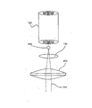
Classifications
-
- G—PHYSICS
- G02—OPTICS
- G02B—OPTICAL ELEMENTS, SYSTEMS OR APPARATUS
- G02B6/00—Light guides; Structural details of arrangements comprising light guides and other optical elements, e.g. couplings
- G02B6/24—Coupling light guides
- G02B6/42—Coupling light guides with opto-electronic elements
- G02B6/4201—Packages, e.g. shape, construction, internal or external details
- G02B6/4202—Packages, e.g. shape, construction, internal or external details for coupling an active element with fibres without intermediate optical elements, e.g. fibres with plane ends, fibres with shaped ends, bundles
-
- G—PHYSICS
- G02—OPTICS
- G02B—OPTICAL ELEMENTS, SYSTEMS OR APPARATUS
- G02B6/00—Light guides; Structural details of arrangements comprising light guides and other optical elements, e.g. couplings
- G02B6/02—Optical fibres with cladding with or without a coating
- G02B6/0229—Optical fibres with cladding with or without a coating characterised by nanostructures, i.e. structures of size less than 100 nm, e.g. quantum dots
-
- B—PERFORMING OPERATIONS; TRANSPORTING
- B82—NANOTECHNOLOGY
- B82Y—SPECIFIC USES OR APPLICATIONS OF NANOSTRUCTURES; MEASUREMENT OR ANALYSIS OF NANOSTRUCTURES; MANUFACTURE OR TREATMENT OF NANOSTRUCTURES
- B82Y10/00—Nanotechnology for information processing, storage or transmission, e.g. quantum computing or single electron logic
-
- B—PERFORMING OPERATIONS; TRANSPORTING
- B82—NANOTECHNOLOGY
- B82Y—SPECIFIC USES OR APPLICATIONS OF NANOSTRUCTURES; MEASUREMENT OR ANALYSIS OF NANOSTRUCTURES; MANUFACTURE OR TREATMENT OF NANOSTRUCTURES
- B82Y20/00—Nanooptics, e.g. quantum optics or photonic crystals
-
- B—PERFORMING OPERATIONS; TRANSPORTING
- B82—NANOTECHNOLOGY
- B82Y—SPECIFIC USES OR APPLICATIONS OF NANOSTRUCTURES; MEASUREMENT OR ANALYSIS OF NANOSTRUCTURES; MANUFACTURE OR TREATMENT OF NANOSTRUCTURES
- B82Y30/00—Nanotechnology for materials or surface science, e.g. nanocomposites
-
- G—PHYSICS
- G02—OPTICS
- G02B—OPTICAL ELEMENTS, SYSTEMS OR APPARATUS
- G02B6/00—Light guides; Structural details of arrangements comprising light guides and other optical elements, e.g. couplings
- G02B6/10—Light guides; Structural details of arrangements comprising light guides and other optical elements, e.g. couplings of the optical waveguide type
- G02B6/12—Light guides; Structural details of arrangements comprising light guides and other optical elements, e.g. couplings of the optical waveguide type of the integrated circuit kind
- G02B2006/12083—Constructional arrangements
- G02B2006/1213—Constructional arrangements comprising photonic band-gap structures or photonic lattices
-
- G—PHYSICS
- G02—OPTICS
- G02B—OPTICAL ELEMENTS, SYSTEMS OR APPARATUS
- G02B6/00—Light guides; Structural details of arrangements comprising light guides and other optical elements, e.g. couplings
- G02B6/02—Optical fibres with cladding with or without a coating
- G02B6/02295—Microstructured optical fibre
- G02B6/02314—Plurality of longitudinal structures extending along optical fibre axis, e.g. holes
- G02B6/02319—Plurality of longitudinal structures extending along optical fibre axis, e.g. holes characterised by core or core-cladding interface features
- G02B6/02323—Core having lower refractive index than cladding, e.g. photonic band gap guiding
- G02B6/02328—Hollow or gas filled core
-
- G—PHYSICS
- G02—OPTICS
- G02B—OPTICAL ELEMENTS, SYSTEMS OR APPARATUS
- G02B6/00—Light guides; Structural details of arrangements comprising light guides and other optical elements, e.g. couplings
- G02B6/02—Optical fibres with cladding with or without a coating
- G02B6/02295—Microstructured optical fibre
- G02B6/02314—Plurality of longitudinal structures extending along optical fibre axis, e.g. holes
- G02B6/02342—Plurality of longitudinal structures extending along optical fibre axis, e.g. holes characterised by cladding features, i.e. light confining region
- G02B6/02366—Single ring of structures, e.g. "air clad"
-
- G—PHYSICS
- G02—OPTICS
- G02B—OPTICAL ELEMENTS, SYSTEMS OR APPARATUS
- G02B6/00—Light guides; Structural details of arrangements comprising light guides and other optical elements, e.g. couplings
- G02B6/24—Coupling light guides
- G02B6/42—Coupling light guides with opto-electronic elements
- G02B6/4201—Packages, e.g. shape, construction, internal or external details
- G02B6/4219—Mechanical fixtures for holding or positioning the elements relative to each other in the couplings; Alignment methods for the elements, e.g. measuring or observing methods especially used therefor
- G02B6/4228—Passive alignment, i.e. without a detection of the degree of coupling or the position of the elements
- G02B6/423—Passive alignment, i.e. without a detection of the degree of coupling or the position of the elements using guiding surfaces for the alignment
Landscapes
- Physics & Mathematics (AREA)
- General Physics & Mathematics (AREA)
- Optics & Photonics (AREA)
- Chemical & Material Sciences (AREA)
- Crystallography & Structural Chemistry (AREA)
- Optical Modulation, Optical Deflection, Nonlinear Optics, Optical Demodulation, Optical Logic Elements (AREA)
- Optical Integrated Circuits (AREA)
Applications Claiming Priority (3)
| Application Number | Priority Date | Filing Date | Title |
|---|---|---|---|
| US11/444,222 US7546013B1 (en) | 2006-05-31 | 2006-05-31 | Nanoparticle coupled to waveguide |
| US11/444,222 | 2006-05-31 | ||
| PCT/US2007/012242 WO2007142826A2 (en) | 2006-05-31 | 2007-05-22 | Nanoparticle coupled to waveguide |
Publications (2)
| Publication Number | Publication Date |
|---|---|
| JP2009539140A JP2009539140A (ja) | 2009-11-12 |
| JP4871994B2 true JP4871994B2 (ja) | 2012-02-08 |
Family
ID=38801969
Family Applications (1)
| Application Number | Title | Priority Date | Filing Date |
|---|---|---|---|
| JP2009513177A Expired - Fee Related JP4871994B2 (ja) | 2006-05-31 | 2007-05-22 | 導波路に結合されるナノ粒子 |
Country Status (4)
| Country | Link |
|---|---|
| US (1) | US7546013B1 (de) |
| EP (1) | EP2022145A2 (de) |
| JP (1) | JP4871994B2 (de) |
| WO (1) | WO2007142826A2 (de) |
Families Citing this family (15)
| Publication number | Priority date | Publication date | Assignee | Title |
|---|---|---|---|---|
| US9297092B2 (en) | 2005-06-05 | 2016-03-29 | Qd Vision, Inc. | Compositions, optical component, system including an optical component, devices, and other products |
| US8718437B2 (en) | 2006-03-07 | 2014-05-06 | Qd Vision, Inc. | Compositions, optical component, system including an optical component, devices, and other products |
| US8849087B2 (en) | 2006-03-07 | 2014-09-30 | Qd Vision, Inc. | Compositions, optical component, system including an optical component, devices, and other products |
| US9874674B2 (en) | 2006-03-07 | 2018-01-23 | Samsung Electronics Co., Ltd. | Compositions, optical component, system including an optical component, devices, and other products |
| US7427525B2 (en) * | 2006-10-13 | 2008-09-23 | Hewlett-Packard Development Company, L.P. | Methods for coupling diamond structures to photonic devices |
| US20090034737A1 (en) * | 2007-07-30 | 2009-02-05 | Magiq Technologies, Inc. | Diamond nanocrystal single-photon source with wavelength converter |
| US9207385B2 (en) | 2008-05-06 | 2015-12-08 | Qd Vision, Inc. | Lighting systems and devices including same |
| WO2009151515A1 (en) | 2008-05-06 | 2009-12-17 | Qd Vision, Inc. | Solid state lighting devices including quantum confined semiconductor nanoparticles |
| WO2009137053A1 (en) | 2008-05-06 | 2009-11-12 | Qd Vision, Inc. | Optical components, systems including an optical component, and devices |
| JP5468091B2 (ja) * | 2009-02-27 | 2014-04-09 | 延世大學校産學協力財団 | 構造物の変形測定用装置及びそれを用いた構造物の変形測定方法 |
| US8842949B2 (en) | 2010-09-02 | 2014-09-23 | Technische Universitat Darmstadt | Single photon emission system |
| WO2013066446A1 (en) | 2011-08-01 | 2013-05-10 | The Trustees Of Columbia University In The City Of New York | Conjugates of nano-diamond and magnetic or metallic particles |
| WO2013040446A1 (en) * | 2011-09-16 | 2013-03-21 | The Trustees Of Columbia University In The City Of New York | High-precision ghz clock generation using spin states in diamond |
| US9632045B2 (en) | 2011-10-19 | 2017-04-25 | The Trustees Of Columbia University In The City Of New York | Systems and methods for deterministic emitter switch microscopy |
| WO2020180391A1 (en) * | 2019-03-05 | 2020-09-10 | Massachusetts Institute Of Technology | Scalable integration of hybrid optoelectronic and quantum optical systems into photonic circuits |
Family Cites Families (14)
| Publication number | Priority date | Publication date | Assignee | Title |
|---|---|---|---|---|
| US5422907A (en) * | 1994-05-20 | 1995-06-06 | Bhargava; Rameshwar N. | Pumped solid-state lasers comprising doped nanocrystal phosphors |
| US7019333B1 (en) * | 1999-11-16 | 2006-03-28 | Kabushiki Kaisha Toshiba | Photon source |
| FR2809542B1 (fr) | 2000-05-29 | 2005-02-25 | France Telecom | Source a un photon a base d'emetteurs dont les frequences sont reparties de maniere choisie |
| GB2366666B (en) * | 2000-09-11 | 2002-12-04 | Toshiba Res Europ Ltd | An optical device and method for its manufacture |
| US6697548B2 (en) * | 2000-12-18 | 2004-02-24 | Evident Technologies | Fabry-perot opitcal switch having a saturable absorber |
| US7132676B2 (en) * | 2001-05-15 | 2006-11-07 | Kabushiki Kaisha Toshiba | Photon source and a method of operating a photon source |
| US20020186921A1 (en) * | 2001-06-06 | 2002-12-12 | Schumacher Lynn C. | Multiwavelength optical fiber devices |
| US20030044114A1 (en) * | 2001-09-06 | 2003-03-06 | Pelka David G. | Source wavelength shifting apparatus and method for delivery of one or more selected emission wavelengths |
| US6853669B2 (en) | 2002-12-10 | 2005-02-08 | Ut-Battelle, Llc | Nanocrystal waveguide (NOW) laser |
| EP1503328B1 (de) | 2003-07-29 | 2007-05-23 | Hitachi, Ltd. | Einzelphotonenquelle |
| AU2005219894A1 (en) * | 2004-03-02 | 2005-09-15 | The University Of Melbourne | A photon source |
| JP2006060143A (ja) * | 2004-08-23 | 2006-03-02 | Nec Corp | 光ファイバ型単一光子発生素子および単一光子発生装置 |
| US20060165895A1 (en) * | 2005-01-24 | 2006-07-27 | Julio Cartagena | System and a method for synthesizing nanoparticle arrays in-situ |
| US7492803B2 (en) * | 2005-06-10 | 2009-02-17 | Hewlett-Packard Development Company, L.P. | Fiber-coupled single photon source |
-
2006
- 2006-05-31 US US11/444,222 patent/US7546013B1/en active Active
-
2007
- 2007-05-22 JP JP2009513177A patent/JP4871994B2/ja not_active Expired - Fee Related
- 2007-05-22 EP EP07777226A patent/EP2022145A2/de not_active Withdrawn
- 2007-05-22 WO PCT/US2007/012242 patent/WO2007142826A2/en not_active Ceased
Also Published As
| Publication number | Publication date |
|---|---|
| US7546013B1 (en) | 2009-06-09 |
| US20090140275A1 (en) | 2009-06-04 |
| JP2009539140A (ja) | 2009-11-12 |
| WO2007142826A2 (en) | 2007-12-13 |
| WO2007142826A3 (en) | 2008-03-13 |
| EP2022145A2 (de) | 2009-02-11 |
Similar Documents
| Publication | Publication Date | Title |
|---|---|---|
| JP4871994B2 (ja) | 導波路に結合されるナノ粒子 | |
| JP5068256B2 (ja) | ファイバ結合された単一光子源 | |
| CN109075532B (zh) | 高速vcsel装置 | |
| US11152760B2 (en) | Light emitter device based on a photonic crystal with pillar- or wall-shaped semiconductor elements, and methods for the operation and production thereof | |
| US7783140B2 (en) | Optically coupled integrated circuit layers | |
| US20100258784A1 (en) | Method Of Efficient Coupling Of Light From Single-Photon Emitter To Guided Radiation Localized To Sub-Wavelength Dimensions On Conducting Nanowires | |
| JP5317122B2 (ja) | 単一光子発生装置 | |
| JP2011192876A (ja) | フォトニック結晶光源装置 | |
| JP2019039984A (ja) | 光デバイス及びその製造方法 | |
| CN102684072A (zh) | 混合集成激光器及其制备方法 | |
| US20100066238A1 (en) | Electrically tunable plasmon light tunneling junction | |
| US20250324820A1 (en) | Quantum light source with dual optical cavities | |
| US20200059062A1 (en) | Systems and methods for end pumped laser mirror stack assemblies | |
| US7570849B2 (en) | Integrated circuit device having optically coupled layers | |
| KR20210090041A (ko) | 양자 광원 제조 방법 및 양자 광원을 이용한 양자 광 전송 장치 | |
| US11520105B2 (en) | Single photon source | |
| KR102822108B1 (ko) | 단광자 광원 | |
| KR102955086B1 (ko) | 조명 유닛, 조명 유닛을 제조하기 위한 방법, 광전자 부품을 위한 변환체 요소, led 및 변환체 요소를 갖는 복사선 소스, 커플링-아웃 구조, 및 광전자 장치 | |
| GB2637144A (en) | Coupled laser array | |
| GR20230100588A (el) | Συζευξη φωτος μεταξυ νανοκαλωδιου και οπτικου κυματοδηγου μεσω φωτονικου νανοπιδακα μικροσφαιριδιου | |
| Paniccia et al. | A hybrid silicon laser | |
| CN115733559A (zh) | 片上集成单光子源发光增强装置及其制备方法 | |
| KR20260046251A (ko) | 조명 유닛, 조명 유닛을 제조하기 위한 방법, 광전자 부품을 위한 변환체 요소, led 및 변환체 요소를 갖는 복사선 소스, 커플링-아웃 구조, 및 광전자 장치 | |
| Bisschop et al. | Progress towards on-chip single photon sources based on colloidal quantum dots in silicon nitride devices | |
| Hecht | PHOTONIC FRONTIERS: SILICON PHOTONICS-Closing in on silicon lasers-Lasing isn't impossible in semiconductors with indirect bandgaps, but it is difficult, which makes the quest for silicon lasers |
Legal Events
| Date | Code | Title | Description |
|---|---|---|---|
| A131 | Notification of reasons for refusal |
Free format text: JAPANESE INTERMEDIATE CODE: A131 Effective date: 20100727 |
|
| A521 | Request for written amendment filed |
Free format text: JAPANESE INTERMEDIATE CODE: A523 Effective date: 20101012 |
|
| A02 | Decision of refusal |
Free format text: JAPANESE INTERMEDIATE CODE: A02 Effective date: 20110329 |
|
| A521 | Request for written amendment filed |
Free format text: JAPANESE INTERMEDIATE CODE: A523 Effective date: 20110721 |
|
| A911 | Transfer to examiner for re-examination before appeal (zenchi) |
Free format text: JAPANESE INTERMEDIATE CODE: A911 Effective date: 20110728 |
|
| TRDD | Decision of grant or rejection written | ||
| A01 | Written decision to grant a patent or to grant a registration (utility model) |
Free format text: JAPANESE INTERMEDIATE CODE: A01 Effective date: 20111115 |
|
| A01 | Written decision to grant a patent or to grant a registration (utility model) |
Free format text: JAPANESE INTERMEDIATE CODE: A01 |
|
| A61 | First payment of annual fees (during grant procedure) |
Free format text: JAPANESE INTERMEDIATE CODE: A61 Effective date: 20111121 |
|
| R150 | Certificate of patent or registration of utility model |
Ref document number: 4871994 Country of ref document: JP Free format text: JAPANESE INTERMEDIATE CODE: R150 Free format text: JAPANESE INTERMEDIATE CODE: R150 |
|
| FPAY | Renewal fee payment (event date is renewal date of database) |
Free format text: PAYMENT UNTIL: 20141125 Year of fee payment: 3 |
|
| R250 | Receipt of annual fees |
Free format text: JAPANESE INTERMEDIATE CODE: R250 |
|
| R250 | Receipt of annual fees |
Free format text: JAPANESE INTERMEDIATE CODE: R250 |
|
| S111 | Request for change of ownership or part of ownership |
Free format text: JAPANESE INTERMEDIATE CODE: R313113 |
|
| R360 | Written notification for declining of transfer of rights |
Free format text: JAPANESE INTERMEDIATE CODE: R360 |
|
| R360 | Written notification for declining of transfer of rights |
Free format text: JAPANESE INTERMEDIATE CODE: R360 |
|
| R371 | Transfer withdrawn |
Free format text: JAPANESE INTERMEDIATE CODE: R371 |
|
| R250 | Receipt of annual fees |
Free format text: JAPANESE INTERMEDIATE CODE: R250 |
|
| S111 | Request for change of ownership or part of ownership |
Free format text: JAPANESE INTERMEDIATE CODE: R313113 |
|
| R350 | Written notification of registration of transfer |
Free format text: JAPANESE INTERMEDIATE CODE: R350 |
|
| R250 | Receipt of annual fees |
Free format text: JAPANESE INTERMEDIATE CODE: R250 |
|
| R250 | Receipt of annual fees |
Free format text: JAPANESE INTERMEDIATE CODE: R250 |
|
| R250 | Receipt of annual fees |
Free format text: JAPANESE INTERMEDIATE CODE: R250 |
|
| R250 | Receipt of annual fees |
Free format text: JAPANESE INTERMEDIATE CODE: R250 |
|
| R250 | Receipt of annual fees |
Free format text: JAPANESE INTERMEDIATE CODE: R250 |
|
| R250 | Receipt of annual fees |
Free format text: JAPANESE INTERMEDIATE CODE: R250 |
|
| R250 | Receipt of annual fees |
Free format text: JAPANESE INTERMEDIATE CODE: R250 |
|
| LAPS | Cancellation because of no payment of annual fees |