JP4868576B2 - Image processing device - Google Patents
Image processing device Download PDFInfo
- Publication number
- JP4868576B2 JP4868576B2 JP2006018764A JP2006018764A JP4868576B2 JP 4868576 B2 JP4868576 B2 JP 4868576B2 JP 2006018764 A JP2006018764 A JP 2006018764A JP 2006018764 A JP2006018764 A JP 2006018764A JP 4868576 B2 JP4868576 B2 JP 4868576B2
- Authority
- JP
- Japan
- Prior art keywords
- counter
- image
- image processing
- color
- data
- Prior art date
- Legal status (The legal status is an assumption and is not a legal conclusion. Google has not performed a legal analysis and makes no representation as to the accuracy of the status listed.)
- Expired - Fee Related
Links
Images


Classifications
-
- H—ELECTRICITY
- H04—ELECTRIC COMMUNICATION TECHNIQUE
- H04N—PICTORIAL COMMUNICATION, e.g. TELEVISION
- H04N23/00—Cameras or camera modules comprising electronic image sensors; Control thereof
- H04N23/80—Camera processing pipelines; Components thereof
- H04N23/84—Camera processing pipelines; Components thereof for processing colour signals
- H04N23/843—Demosaicing, e.g. interpolating colour pixel values
-
- H—ELECTRICITY
- H04—ELECTRIC COMMUNICATION TECHNIQUE
- H04N—PICTORIAL COMMUNICATION, e.g. TELEVISION
- H04N23/00—Cameras or camera modules comprising electronic image sensors; Control thereof
- H04N23/80—Camera processing pipelines; Components thereof
- H04N23/84—Camera processing pipelines; Components thereof for processing colour signals
- H04N23/88—Camera processing pipelines; Components thereof for processing colour signals for colour balance, e.g. white-balance circuits or colour temperature control
-
- H—ELECTRICITY
- H04—ELECTRIC COMMUNICATION TECHNIQUE
- H04N—PICTORIAL COMMUNICATION, e.g. TELEVISION
- H04N25/00—Circuitry of solid-state image sensors [SSIS]; Control thereof
- H04N25/10—Circuitry of solid-state image sensors [SSIS]; Control thereof for transforming different wavelengths into image signals
- H04N25/11—Arrangement of colour filter arrays [CFA]; Filter mosaics
- H04N25/13—Arrangement of colour filter arrays [CFA]; Filter mosaics characterised by the spectral characteristics of the filter elements
- H04N25/134—Arrangement of colour filter arrays [CFA]; Filter mosaics characterised by the spectral characteristics of the filter elements based on three different wavelength filter elements
-
- H—ELECTRICITY
- H04—ELECTRIC COMMUNICATION TECHNIQUE
- H04N—PICTORIAL COMMUNICATION, e.g. TELEVISION
- H04N25/00—Circuitry of solid-state image sensors [SSIS]; Control thereof
- H04N25/70—SSIS architectures; Circuits associated therewith
Description
この発明は、複数の画像データ読み出しチャンネルを有する画像センサーに特有の補正処理(黒レベル補正、ホワイトバランス補正等)を行う画像処理装置に関する。 The present invention relates to an image processing apparatus that performs correction processing (black level correction, white balance correction, etc.) unique to an image sensor having a plurality of image data readout channels.
図23は、従来技術に於ける、デジタル(スチル、ビデオ)カメラ用画像処理LSIの構成を模式的に示すブロック図である。本装置に於いては、画像センサーPISの画像データ読み出しチャンネルRCH0は1チャンネルであり、その結果、各画素に於ける画像データは線順位にラスタースキャンされて順次に読み出される。そして、画像センサーPISの有効画素領域内の各画素に設けられた色フィルタの配列(色の並び方)は、所謂、RGB Bayer(RGBベイヤー)配列となっている。 FIG. 23 is a block diagram schematically showing a configuration of an image processing LSI for a digital (still, video) camera in the prior art. In this apparatus, the image data reading channel RCH0 of the image sensor PIS is one channel, and as a result, the image data in each pixel is raster-scanned in line order and sequentially read out. The arrangement (color arrangement) of the color filters provided in each pixel in the effective pixel area of the image sensor PIS is a so-called RGB Bayer (RGB Bayer) arrangement.
画素クロック(図示せず)に応じて画像センサーPISから順次に読み出された画像データは先ずA/D変換器300PによってA/D変換された上で、C−MOS LSI上の画像センサーデータ前処理ユニット(以下、SPU(センサープロセッシングユニット)と言う。)100Pに入力される。SPU100Pは、本来的な画像処理を行う回路では無く、画像センサーPISに特有の問題点に起因した処理を、即ち、黒レベル補正、ホワイトバランス補正及び欠陥画素補正を画像センサーPISからの入力画像データに対して実行して、正規化されたRGB Bayer信号を得るユニットである。
Image data sequentially read out from the image sensor PIS according to a pixel clock (not shown) is first A / D converted by the A /
画像センサーPISから入力されるRGB Bayer信号の正規化処理を模式的に示した図が図24であり、本図24は後述する実施の形態1に於いても援用される図面である。図24(a)に示されるR(赤)、G(緑)及びB(青)の各色信号は線形性を有することが前提となっており、各色信号は黒レベル補正を施されて、それらの原点が揃えられる(図24(b)参照。)。更に、各色信号はホワイトバランス補正を施されて、それらの特性は重なり合い、正規化される(図24(c)参照。)。 FIG. 24 is a diagram schematically showing normalization processing of RGB Bayer signals input from the image sensor PIS, and FIG. 24 is also used in the first embodiment described later. Each color signal of R (red), G (green), and B (blue) shown in FIG. 24 (a) is assumed to have linearity, and each color signal is subjected to black level correction. Are aligned (see FIG. 24B). Further, each color signal is subjected to white balance correction, and their characteristics are overlapped and normalized (see FIG. 24C).
正規化されたRGB Bayer信号は、次にRPU200Pに入力されて、γ補正等の本来的な画像処理を施される。
The normalized RGB Bayer signal is then input to the
図25は、従来技術に於けるSPU100Pの主要部分の構成を模式的に示すブロック図である。同図に於いて、グローバルHカウンタ1は、画素クロックCLKを入力信号としてその受信数をカウントすることでカウント値HCNTを生成して、画像センサーPISからの画像データの水平方向に於ける読み出しタイミングを定義乃至は管理するグローバル水平方向カウンタである。又、グローバルVカウンタ2は、画素クロックCLKに同期して、グローバルHカウンタ1のキャリーアウトCOから出力されるリセット信号を受信する毎にそのカウント値VCNTを1ずつインクリメントすることで、画像センサーPISからの画像データの垂直方向に於ける読み出しタイミングを定義乃至は管理するグローバル垂直方向カウンタである。尚、両カウンタ1,2は後述する実施の形態1でも適用される構成要素である。SPU100Pでは、画像センサーPISの読み出しチャンネルが1チャンネルであるため、RGB Bayer配列の下では、補正データを読み出すためのタイミング信号の繰り返し範囲は、2×2で良い。従って、グローバルHカウンタ1のカウント値HCNTの最下位ビットHCNT(0)とグローバルVカウンタ2のカウント値VCNTの最下位ビットVCNT(0)との合成によって、2ビットの色選択タイミング信号COLSELが生成される。又、予め、黒レベル補正値用レジスタBLRが、SPU100P内に配備されている。ここで、黒レベル補正値用レジスタBLRは、RGB Bayer配列下での各色(全4色)が割り当てられる上記2×2の繰り返し範囲の各場所に於ける黒レベル補正値をそれぞれ格納するレジスタBL0〜BL3を有する。即ち、レジスタBL0は、上記繰り返し範囲内の00位置に於ける色Rの黒レベル補正値を格納しており、レジスタBL1は、上記繰り返し範囲内の01位置に於ける色Grの黒レベル補正値を格納しており、レジスタBL2は、上記繰り返し範囲内の10位置に於ける色Gbの黒レベル補正値を格納しており、レジスタBL3は、上記繰り返し範囲内の11位置に於ける色Bの黒レベル補正値を格納している。同様に、ホワイトバランス補正値用レジスタWBRも、SPU100P内に配備されている。そして、SPU100Pで特筆すべき点は、図25に示されている通り、各色の各場所に於ける黒レベル補正値及びホワイトバランス補正値が共に、対応するセレクタ11P,12Pを介して、色選択タイミング信号COLSELによって直接的に選択されているところにある。尚、参照符号13P及び14Pは、それぞれ、黒レベル補正処理部及びホワイトバランス補正処理部である。
FIG. 25 is a block diagram schematically showing the configuration of the main part of the
<問題点その1>
より高画質の画像生成を求めて、画像センサー(CCDセンサー又はCMOSセンサー等)の高精細化、従って、画素数の増大化が求められている。斯かる要求に応じて、画素数が8Mピクセルあるいは10Mピクセル以上の画像センサーが実現されるに至っている。この様な画像センサーの画素数の増大化に対して、斯かる画像センサーを使用するデジタルスチルカメラメーカーは、単位時間当たりのコマ数、即ち、連写速度の維持乃至は更なる向上を追及している。このため、例えば、画素数が3Mピクセルの場合に連写速度が10コマ/秒であるとしたときには、データレート乃至は画像データ読み出しレートは30Mピクセル/秒となり、この連写速度を維持するならば、画素数が5Mピクセルの場合には画像データ読み出しレートは50Mピクセル/秒に、画素数が8Mピクセルの場合には画像データ読み出しレートは80Mピクセル/秒に、画素数が10Mピクセルの場合には画像データ読み出しレートは100Mピクセル/秒にも達する。それにも拘らず、CCDセンサーの動作スピードの最大値は35MHz程度であり、又、CMOSセンサーの場合には、その最大値は50MHz〜100MHz程度である。又、C−MOS LSIの動作速度は約100MHz程度である。画像センサーを低価格で且つ低消費電力で作成しようとする場合には、画像センサーの動作スピードの最大値は40MHz程度であることが望ましい。そうすると、1チャンネルで画像データを画像センサーから読み出している限り、既述した読み出しレートが50Mピクセル/秒以上となる連写速度を維持・実現することは不可能となる。この様な問題点を根本的に解決するためには、画像センサーの画像データの読み出しチャンネル数を増やす必要性がある。斯かる必要性に応じて、昨今では、複数の読み出しチャンネルを有する画像センサーが実現されるに至っている。
<
In search of higher quality image generation, there is a demand for higher definition of image sensors (CCD sensors, CMOS sensors, etc.), and hence an increase in the number of pixels. In response to such a demand, an image sensor having 8M pixels or 10M pixels or more has been realized. In response to such an increase in the number of pixels of an image sensor, a digital still camera manufacturer using such an image sensor seeks to maintain or further improve the number of frames per unit time, that is, the continuous shooting speed. ing. Therefore, for example, if the continuous shooting speed is 10 frames / second when the number of pixels is 3M pixels, the data rate or the image data reading rate is 30M pixels / second, and this continuous shooting speed is maintained. For example, when the number of pixels is 5M pixels, the image data readout rate is 50M pixels / second, when the number of pixels is 8M pixels, the image data readout rate is 80M pixels / second, and when the number of pixels is 10M pixels. The image data read rate reaches 100M pixels / second. Nevertheless, the maximum value of the operating speed of the CCD sensor is about 35 MHz, and in the case of the CMOS sensor, the maximum value is about 50 MHz to 100 MHz. The operation speed of the C-MOS LSI is about 100 MHz. When an image sensor is to be produced at low cost and low power consumption, the maximum value of the operation speed of the image sensor is preferably about 40 MHz. As a result, as long as image data is read from the image sensor in one channel, it is impossible to maintain and realize the continuous shooting speed at which the reading rate described above is 50 Mpixels / second or more. In order to fundamentally solve such problems, it is necessary to increase the number of image data read channels of the image sensor. In response to such a need, an image sensor having a plurality of readout channels has recently been realized.
この様な読み出しチャンネル数の増大化に伴い、様々な画像データの読み出しパターンが提案・実現されるに至っており、この様な画像データの読み出しパターンの多様化に如何に対応すべきかと言う新たな問題点が生じている。この点につき、読み出しチャンネル数が2である場合について以下に簡単に考察することとする。 With such an increase in the number of read channels, various image data read patterns have been proposed and realized, and new ways to deal with such diversification of image data read patterns have been proposed. There is a problem. In this regard, the case where the number of read channels is 2 will be briefly considered below.
例えば、RGB Bayer配列の下に於いて、読み出しチャンネル数が2である場合の読み出しパターンとして、図26に示すパターンが一例として考えられる。この読み出しパターンでは、第1番目の読み出しチャンネルRCH0より、画像センサーのある偶数ラインに属するR色の画像データのみを読み出す一方、第2番目の読み出しチャンネルRCH1より、当該偶数ラインに属するGr色の画像データのみを読み出す。次の奇数ラインでは、第1番目の読み出しチャンネルRCH0よりGb色の画像データのみを読み出し、第2番目の読み出しチャンネルRCH1よりB色の画像データのみを読み出す。あるいは、その変形例として、画像センサーのある偶数ラインに属するR色及びGr色の画像データを第1番目の読み出しチャンネルRCH0より読み出す一方、次の奇数ラインに属するGb色及びB色の画像データを第2番目の読み出しチャンネルRCH1より読み出すと言うパターン例も有り得る。 For example, the pattern shown in FIG. 26 can be considered as an example of a read pattern when the number of read channels is 2 under the RGB Bayer array. In this readout pattern, only the R color image data belonging to an even line with an image sensor is read out from the first readout channel RCH0, while the Gr color image belonging to the even line from the second readout channel RCH1. Read data only. In the next odd line, only Gb color image data is read from the first read channel RCH0, and only B color image data is read from the second read channel RCH1. Alternatively, as a modification thereof, the R and Gr color image data belonging to an even line with an image sensor is read from the first read channel RCH0, while the Gb and B color image data belonging to the next odd line is read. There may be a pattern example of reading from the second read channel RCH1.
RGB Bayer配列下に於いて、更なる一例として、図27に示すパターンが考えられる。更に、図28に示す様に、画像センサーのRGB Bayer配列をその中央より左右に2分化して、あるラインに於いて左側から順次に読み出す一方、右側からも順次に読み出すと言う読み出しパターンも提案・実現されている。更には、画像センサーのRGB Bayer配列のある領域では縦方向に読み出す一方、その他の領域では水平方向に読み出すと言う読み出しパターンも提案されている。 As a further example under the RGB Bayer arrangement, the pattern shown in FIG. 27 can be considered. Furthermore, as shown in FIG. 28, the RGB Bayer array of the image sensor is divided into two from the center to the left and right, and a reading pattern is also proposed in which reading is sequentially performed from the left side in a certain line, while also sequentially reading from the right side.・ It is realized. Furthermore, a reading pattern has been proposed in which reading is performed in the vertical direction in a certain region of the RGB Bayer array of the image sensor, while reading is performed in the horizontal direction in other regions.
この様に、読み出しチャンネル数が2である場合でも上記の通り様々な読み出しパターンが提案されている。そうすると、読み出しチャンネル数がそれ以上に増えるときには、読み出しパターンはより複雑化して、その数は鰻登りに増大化する。 Thus, even when the number of read channels is 2, various read patterns have been proposed as described above. Then, when the number of read channels increases further, the read pattern becomes more complicated, and the number increases ascending.
以上の通り、画像センサーのメーカー毎に、あるいは、同一メーカー内の製品であってもその型番毎に、画像センサーからの読み出しパターンは千差万別であると言える。従って、画像センサーから読み出された画像データに対して画像処理を施す汎用LSI(画像処理装置)を設計・製作する側から見れば、デジタルカメラメーカーが採用する画像センサーが如何なる画像読み出しパターンを有していようとも、その画像読み出しパターンに対して常に対応可能な汎用性に富んだ画像処理LSIを提供する必要性が有ると言える。この様な問題点は早急に対応を求められる課題である。 As described above, it can be said that there are various reading patterns from the image sensor for each manufacturer of the image sensor, or for each product number even if the product is in the same manufacturer. Therefore, from the viewpoint of designing and manufacturing a general-purpose LSI (image processing apparatus) that performs image processing on image data read from the image sensor, the image sensor employed by the digital camera manufacturer has any image reading pattern. Even so, it can be said that there is a need to provide a versatile image processing LSI that can always cope with the image reading pattern. Such problems are issues that require immediate attention.
<問題点その2>
既述の通り、画像センサーに於ける画素数の増大化に伴い、画像センサーの有効画素領域は同じであるため、画像センサーに於ける各セルのサイズはより一層小さくならざるを得なくなる。この様に画像センサーの各セルの微細化に伴い、各セルの出力信号のレベルは相対的に小さくなり、従って、出力信号の線形性も損なわれて来る。このため、画像センサーの有効画素領域内の場所毎に、あるいは、ライン毎に、その特性が異なるセルが頻出して来る。そのため、画像センサーの有効画素領域内の場所毎に、各画素のRGB Bayer信号を正規化するために必要な黒レベル補正値及びホワイトバランス補正値が異なって来ることとなる。この様な画像センサーの各セルの微細化に伴い生じる上記の問題点を克服して、各画素のRGB Bayer信号を高精度で補正することが求められる。
<
As described above, since the effective pixel area of the image sensor is the same as the number of pixels in the image sensor increases, the size of each cell in the image sensor must be further reduced. As described above, with the miniaturization of each cell of the image sensor, the level of the output signal of each cell becomes relatively small, and therefore the linearity of the output signal is also impaired. For this reason, cells having different characteristics frequently appear for each location in the effective pixel region of the image sensor or for each line. Therefore, the black level correction value and the white balance correction value necessary for normalizing the RGB Bayer signal of each pixel differ for each location in the effective pixel region of the image sensor. It is required to correct the RGB Bayer signal of each pixel with high accuracy by overcoming the above-described problems caused by the miniaturization of each cell of such an image sensor.
この発明は、既述した懸案事項に対処すべく成されたものであり、その目的の第1は上記の問題点その1を克服した画像処理装置を提供する点にあり、その目的の第2は上記の問題点その2を克服した画像処理装置を提供する点にある。 The present invention has been made to cope with the above-described concerns, and a first object of the present invention is to provide an image processing apparatus that overcomes the first problem, and a second object of the present invention. Is to provide an image processing apparatus which overcomes the second problem.
この発明の主題は、画像処理装置に於いて、画像センサーが有する複数の画像データ読み出しチャンネルの各々から同期して読み出された各画像信号を当該画像データ読み出しチャンネルに対応する入力チャンネルで画素クロック毎に受信して、受信した画像データに対して前記画像センサーに特有の問題点に起因した所定の画像処理を前記画素クロック毎に並列的に実行するパイプライン型の複数の画像センサー前処理ユニットと、前記複数の画像センサー前処理ユニットの各々の入力チャンネル毎に独立に、ある時点に於ける画素の色を指定する色選択タイミング信号を生成して、各画像センサー前処理ユニットに対して対応する色選択タイミング信号を出力する色タイミングアレンジメント部とを備え、前記色タイミングアレンジメント部は、前記画素クロックに基づき水平方向に於ける画素の読み出しタイミングを定義する水平カウンタと、前記画素クロックに基づき垂直方向に於ける前記画素の読み出しタイミングを定義する垂直カウンタとを備え、前記水平カウンタのカウント値と前記垂直カウンタのカウント値とに基づいて前記色選択タイミング信号を生成し、前記各画像センサー前処理ユニットは当該ユニットに対応する前記色選択タイミング信号に応じて前記所定の画像処理を実行することを特徴とする。 The subject of the present invention is an image processing apparatus in which an image signal read out from each of a plurality of image data readout channels of an image sensor is read out in a pixel clock at an input channel corresponding to the image data readout channel. A plurality of pipeline-type image sensor pre-processing units that receive the received image data and execute predetermined image processing on the received image data in parallel for each pixel clock due to a problem peculiar to the image sensor A color selection timing signal for designating the color of a pixel at a certain point of time independently for each input channel of the plurality of image sensor preprocessing units, and corresponding to each image sensor preprocessing unit and a color timing arrangement unit that outputs the color selection timing signal for the color timing arrangement Men A horizontal counter that defines a pixel readout timing in the horizontal direction based on the pixel clock; and a vertical counter that defines the pixel readout timing in the vertical direction based on the pixel clock. The color selection timing signal is generated based on the count value of the counter and the count value of the vertical counter, and each image sensor pre-processing unit performs the predetermined image processing according to the color selection timing signal corresponding to the unit. It is characterized by performing.
以下、この発明の主題の様々な具体化を、添付図面を基に、その効果・利点と共に、詳述する。 Hereinafter, various embodiments of the subject of the present invention will be described in detail along with the effects and advantages thereof with reference to the accompanying drawings.
請求項1に係る発明によれば、複数の画像データ読み出しチャンネルを有する画像センサーからの様々の読み出しパターンに対応可能な、画像センサーに起因した所定の画像処理を実行する画像処理装置を提供することが出来る。 According to the first aspect of the present invention, there is provided an image processing apparatus capable of corresponding to various readout patterns from an image sensor having a plurality of image data readout channels and executing predetermined image processing caused by the image sensor. I can do it.
請求項2に係る発明によれば、入力チャンネル毎に独立に色選択タイミング信号を確実に生成することが出来る。 According to the second aspect of the present invention, the color selection timing signal can be reliably generated independently for each input channel.
請求項3に係る発明によれば、任意の周期を有するローカルな繰り返し範囲のパターンで以って色選択タイミング信号を生成することが出来る。 According to the third aspect of the present invention, the color selection timing signal can be generated with a pattern of a local repetition range having an arbitrary period.
請求項4に係る発明によれば、色選択タイミング信号の繰り返し範囲を変更することが出来る。
According to the invention of
請求項5に係る発明によれば、色選択タイミング信号の繰り返し範囲を3組合せの範囲内で変更することが出来る。
According to the invention of
請求項6に係る発明によれば、補正データ用レジスタは各画像センサー前処理ユニットの外側に配備されて各ユニットに共通のレジスタとして用いられるため、補正データ用レジスタを各ユニット内に配備する場合と比較して、レジスタを構成するゲート数を格段に削減化して省電力化を図ることが出来る。 According to the sixth aspect of the invention, since the correction data register is provided outside each image sensor preprocessing unit and used as a common register for each unit, the correction data register is provided in each unit. In comparison with, the number of gates constituting the register can be remarkably reduced to save power.
請求項7に係る発明によれば、画像センサーからのデータの読み出しパターンが如何なるパターンであろうとも、入力チャンネル毎に且つ色毎に、画像センサーの微細化に起因した、色の明るさと出力値との非線形特性を補正することが出来る。
According to the invention of
請求項8に係る発明によれば、画像センサーの微細化に起因した非線形特性の補正のみならず、入力チャンネル毎に、画像センサーの出力側の回路系統等その他の原因に起因した非線形特性をも選択的に補正することが出来る。 According to the eighth aspect of the invention, not only correction of nonlinear characteristics due to miniaturization of the image sensor but also nonlinear characteristics due to other causes such as a circuit system on the output side of the image sensor are provided for each input channel. It can be corrected selectively.
請求項9に係る発明によれば、入力チャンネル毎に且つ色毎に、リニアライゼーション処理のクリップを行うことが出来る。 According to the ninth aspect of the invention, linearization processing can be clipped for each input channel and for each color.
請求項10に係る発明によれば、画像センサーの画面全体に渡って発生する、黒レベル信号のオフセットドリフトを軽減化することが出来る。
According to the invention which concerns on
請求項11に係る発明によれば、内挿補間と言う比較的簡単な手法によって各画素位置に於ける黒レベル補正データの変調データを求めることが出来る。
According to the invention of
請求項12に係る発明によれば、黒レベル補正処理に関して、内挿補間の演算式に現れる割り算式をシフト処理で対応可能な2のべき乗の割り算として求めることが出来るので、LSIとして製作される画像処理装置の回路規模の大型化を抑止することが出来る。
According to the invention of
請求項13に係る発明によれば、画像センサーの有効画素領域のサイズに合わせて、両カウンタ出力のビットの選択によって、離散的に配置された複数の黒レベル変調データで以って規定される変調範囲の物理的な広さを変更することが出来る。 According to the thirteenth aspect of the invention, it is defined by a plurality of discretely arranged black level modulation data by selecting bits of both counter outputs in accordance with the size of the effective pixel area of the image sensor. The physical width of the modulation range can be changed.
請求項14に係る発明によれば、変調範囲の中心を画像センサーの有効画素領域の中心に一致させることが出来る。 According to the fourteenth aspect of the present invention, the center of the modulation range can be matched with the center of the effective pixel region of the image sensor.
請求項15に係る発明によれば、画像センサーの画面全体に渡って発生する、ホワイトバランスのオフセットドリフトを軽減化することが出来る。 According to the fifteenth aspect of the present invention, offset drift of white balance that occurs over the entire screen of the image sensor can be reduced.
請求項16に係る発明によれば、内挿補間と言う比較的簡単な手法によって各画素位置に於けるホワイトバランス補正データの変調データを求めることが出来る。 According to the sixteenth aspect of the invention, the modulation data of the white balance correction data at each pixel position can be obtained by a relatively simple method called interpolation.
請求項17に係る発明によれば、ホワイトバランス補正処理に関して、内挿補間の演算式に現れる割り算式をシフト処理で対応可能な2のべき乗の割り算として求めることが出来るので、LSIとして製作される画像処理装置の回路規模の大型化を抑止することが出来る。 According to the seventeenth aspect of the present invention, with respect to the white balance correction process, a division expression appearing in the interpolation interpolation calculation expression can be obtained as a power-of-two division that can be handled by the shift process. An increase in the circuit scale of the image processing apparatus can be suppressed.
請求項18に係る発明によれば、画像センサーの有効画素領域のサイズに合わせて、両カウンタ出力のビットの選択によって、離散的に配置された複数のホワイトバランス変調データで以って規定される変調範囲の物理的な広さを変更することが出来る。 According to the eighteenth aspect of the invention, it is defined by a plurality of discretely arranged white balance modulation data according to the selection of bits of both counter outputs in accordance with the size of the effective pixel area of the image sensor. The physical width of the modulation range can be changed.
請求項19に係る発明によれば、ホワイトバランスゲインの変調範囲の中心を画像センサーの有効画素領域の中心に一致させることが出来る。 According to the nineteenth aspect of the present invention, the center of the white balance gain modulation range can be matched with the center of the effective pixel region of the image sensor.
請求項20に係る発明によれば、画像センサーの画面全体に渡って発生する、尾引き補正ドリフトを軽減化することが出来る。 According to the twentieth aspect of the present invention, it is possible to reduce tail correction drift that occurs over the entire screen of the image sensor.
請求項21に係る発明によれば、内挿補間と言う比較的簡単な手法によって各画素位置に於ける被変調補正ゲインを求めることが出来る。 According to the twenty-first aspect of the invention, the modulation correction gain at each pixel position can be obtained by a relatively simple method called interpolation.
請求項22に係る発明によれば、尾引き補正処理に関して、内挿補間の演算式に現れる割り算式をシフト処理で対応可能な2のべき乗の割り算として求めることが出来るので、LSIとして製作される画像処理装置の回路規模の大型化を抑止することが出来る。
According to the invention of
請求項23に係る発明によれば、画像センサーの有効画素領域のサイズに合わせて、両カウンタ出力のビットの選択によって、離散的に配置された複数の尾引き補正ゲイン変調データで以って規定される変調範囲の物理的な広さを変更することが出来る。
According to the invention of
請求項24に係る発明によれば、尾引き補正ゲインの変調範囲の中心を画像センサーの有効画素領域の中心に一致させることが出来る。 According to the twenty-fourth aspect of the present invention, the center of the modulation range of the tail correction gain can be matched with the center of the effective pixel region of the image sensor.
(実施の形態1)
<複数入力チャンネル下での色選択タイミング信号のプログラマブルな構成>
図1は、本実施の形態に係るデジタル(スチル、ビデオ)カメラ用画像処理LSIの構成を模式的に示すブロック図である。図1の一例では、画像センサー(例えばCCDセンサー又はCMOSセンサー等の固体撮像デバイス)ISの画像データ読み出しチャンネルRCH0〜RCH3の数は4チャンネルである。そして、画像センサーISの有効画素領域内の各画素に設けられた色フィルタの配列(色の並び方)は、既述したRGB Bayer配列となっている。RGB Bayer配列においては、図1に太線で示す様に、R(赤)色の隣に配置されるG(緑)色はR色の影響を受けるため、Gr色として表示され、又、R色の直下に配置されるG色は、その隣に位置するB(青)色の影響を受けるため、Gb色として表示される。
(Embodiment 1)
<Programmable configuration of color selection timing signal under multiple input channels>
FIG. 1 is a block diagram schematically showing a configuration of an image processing LSI for a digital (still, video) camera according to the present embodiment. In the example of FIG. 1, the number of image data readout channels RCH0 to RCH3 of the image sensor (for example, a solid-state imaging device such as a CCD sensor or a CMOS sensor) IS is four. The arrangement (color arrangement) of the color filters provided in each pixel in the effective pixel area of the image sensor IS is the RGB Bayer arrangement described above. In the RGB Bayer array, as indicated by a thick line in FIG. 1, the G (green) color arranged next to the R (red) color is affected by the R color, and is therefore displayed as a Gr color. The G color arranged immediately below is affected by the B (blue) color located next to it, so that it is displayed as the Gb color.
画素クロック(ここでは図示せず。)に応じて各画像データ読み出しチャンネルRCH0〜RCH3から並列的に読み出された画像データは、当該画像データ読み出しチャンネルに対応したA/D変換器300〜303によってA/D変換された上で、C−MOS LSI上のSPU(画像センサーデータ前処理ユニット)100に入力される。ここで、SPU100は、図23のSPU100Pと同様に、画像センサーISに特有の問題点に起因して生じる画像データの補正処理(黒レベル補正、ホワイトバランス補正、欠陥画素補正等の所定の画像処理)を行って、入力したRGB Bayer信号(10ビット〜16ビットのデータ)を正規化する第1画像処理部である(この点に関して既述した図24を参照。)。又、C−MOS LSI上のRPU200は、図23のRPU200Pと同様に、各画像データ読み出しチャンネルRCH0〜RCH3毎に正規化されたRGB Bayer信号に対して本来の画像処理(ガンマ補正、色空間変換処理等)を実施する第2画像処理部である。尚、図1では、図示の便宜上、SPU100の4チャンネルの出力は1本の信号として擬似的に描かれている。本実施の形態の中核部は、SPU100の内部構成にあるので、以下では、SPU100の構成・動作を詳述する。
Image data read in parallel from the image data read channels RCH0 to RCH3 in accordance with a pixel clock (not shown here) is read by the A /
図2は、SPU100の構成の主要部を模式的に示すブロック図である。SPU100は、大別して、(1)画像センサーの画像データ読み出しチャンネル数に対応して4個のユニットから成る第1乃至第4チャンネル用補正処理部SPU−C0〜SPU−C3と、(2)3ビット信号である各チャンネル用色選択タイミング信号C0CS〜C3CSを生成・出力するカラータイミングアレンジメント部10と、(3)第1乃至第4チャンネル用補正処理部SPU−C0〜SPU−C3の各々に共通して用いられる、8種類の各色の黒レベル補正データDL0〜DL7(18ビット信号)及び8種類の各色のホワイトバランス補正データWB0〜WB7(18ビット信号)を格納するSPUレジスタ9とから成る。ここで、Bayer配列では基本的にR,Gr,Gb,Bの4色で各画素の色が特定されるけれども、本実施の形態では、SPU100は8種類の色に対応可能である。これは、既述した図28に示された読み出しパターンにも対応可能とするためである。
FIG. 2 is a block diagram schematically showing the main part of the configuration of the
これらの構成要素の内で、第1乃至第4チャンネル用補正処理部SPU−C0〜SPU−C3は、画像センサーISが有する複数の画像データ読み出しチャンネルの各々から画素クロックに同期して読み出された各画像信号を、当該画像データ読み出しチャンネルに対応する入力チャンネルで画素クロック毎に受信して、受信した画像データ(C0Input〜C3Input)に対して、上記色選択タイミング信号(C0CS〜C3CS)に応じて、上記所定の画像処理を画素クロック毎に並列的に実行する、パイプライン型の複数の入力チャンネル用画像センサー前処理ユニットに該当する。 Among these components, the first to fourth channel correction processing units SPU-C0 to SPU-C3 are read out in synchronization with the pixel clock from each of a plurality of image data readout channels of the image sensor IS. Each image signal is received for each pixel clock through an input channel corresponding to the image data readout channel, and the received image data (C0Input to C3Input) is received according to the color selection timing signal (C0CS to C3CS). This corresponds to a pipeline-type image sensor pre-processing unit for a plurality of input channels that executes the predetermined image processing in parallel for each pixel clock.
又、カラータイミングアレンジメント部10は、本実施の形態の特徴的構成要素の一つであり、画像センサーISからの画像データの読み出しタイミングを定義・管理する水平カウンタ及び垂直カウンタ(何れもこの段階で図示せず。)の両カウント値に基づいて、各入力チャンネル毎に独立にある時点に於ける画素の色を指定する色選択タイミング信号C0CS〜C3CSを生成して、各入力チャンネル用画像センサー前処理ユニットSPU−C0〜SPU−C3に対して対応する色選択タイミング信号を出力する回路である。
The color
第1乃至第4チャンネル用補正処理部SPU−C0〜SPU−C3の各々の入力チャンネルには、画像センサーISから画素クロックに応じて読み出された各画像データC0Input〜C3Inputが並列的に入力する。又、各チャンネル用補正処理部SPU−C0〜SPU−C3の内部構成は互いに同等であるので、それぞれの補正処理部の内部構成の記載を第1チャンネル用補正処理部SPU−C0の内部構成の記載で以って代表させることとする。図2に示す様に、第1セレクタ11C0は、入力する8種類の各色の黒レベル補正データDL0〜DL7の内から、この時点で入力した画像データC0Inputを与える画素位置の色に対応した黒レベル補正データを、入力する第1チャンネル用色選択タイミング信号C0CSの指定値に基づいて選択・出力する。そして、黒レベル補正処理部13C0は、黒レベル補正データDL0〜DL7の内からセレクトされた黒レベル補正データに基づき入力画像データC0Inputに対して黒レベル補正を実行する。更に、第2セレクタ12C0は、入力する8種類の各色のホワイトバランス補正データWB0〜WB7の内から、この時点で入力した画像データC0Inputを与える画素位置の色に対応したホワイトバランス補正データを、同じく第1チャンネル用色選択タイミング信号C0CSの指定値に基づいて選択・出力する。その結果、ホワイトバランス補正処理部14C0は、ホワイトバランス補正データWB0〜WB7の内からセレクトされたホワイトバランス補正データに基づき入力画像データC0Inputに対してホワイトバランス補正データを施して、入力した画像データC0Inputを正規化する。尚、その後に実行される欠陥画素補正処理等の他の処理は、図2では省略されている。 The image data C0Input to C3Input read in accordance with the pixel clock from the image sensor IS are input in parallel to the input channels of the first to fourth channel correction processing units SPU-C0 to SPU-C3. . Further, since the internal configurations of the correction processing units SPU-C0 to SPU-C3 for each channel are equivalent to each other, the description of the internal configuration of each correction processing unit is the same as the internal configuration of the first channel correction processing unit SPU-C0. It will be represented by the description. As shown in FIG. 2, the first selector 11C0 selects the black level corresponding to the color at the pixel position to which the image data C0Input input at this time is selected from among the eight types of black level correction data DL0 to DL7 input. The correction data is selected and output based on the designated value of the input first channel color selection timing signal C0CS. Then, the black level correction processing unit 13C0 performs black level correction on the input image data C0Input based on the black level correction data selected from the black level correction data DL0 to DL7. Further, the second selector 12C0 similarly selects the white balance correction data corresponding to the color at the pixel position to which the image data C0Input inputted at this time is input from among the eight types of white balance correction data WB0 to WB7 inputted. Selection / output is performed based on the designated value of the color selection timing signal C0CS for the first channel. As a result, the white balance correction processing unit 14C0 applies the white balance correction data to the input image data C0Input based on the white balance correction data selected from the white balance correction data WB0 to WB7, and the input image data C0Input. Is normalized. Note that other processes such as a defective pixel correction process executed thereafter are omitted in FIG.
図2に示す通り、本SPU100の特徴点の別の一つは、SPUレジスタ9が、各チャンネル用補正処理部SPU−C0〜SPU−C3の内部に配備されるのではなくて、第1乃至第4各チャンネル用補正処理部SPU−C0〜SPU−C3の外部に別途配備されている点にある。この様なSPUレジスタ9が保有する補正データの共有化により、レジスタを構成するゲート数を格段に削減化して、本SPU100の低消費電力化を達成することが可能となる。
As shown in FIG. 2, another feature point of the
以下では、中核部の一つであるカラータイミングアレンジメント部10の構成・動作を記載することとする。
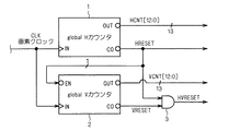
Hereinafter, the configuration and operation of the color
先ず、カラータイミングアレンジメント部10の基本的な構成及び動作を理解し易くすると言う観点から、画像読み出しチャンネル数を2とし、且つ、Bayer配列の下で水平方向に2画素分で垂直方向にも2画素分から構成される2×2の繰り返し範囲乃至は周期で以って画像データを読み出していく場合を想定することとする。その様なケースに於けるカラータイミングアレンジメント部の構成及び繰り返し範囲を図示した図面が、図3である。
First, from the viewpoint of facilitating understanding of the basic configuration and operation of the color
図3に於いて、グローバルHカウンタ1及びグローバルVカウンタ2は、それぞれ、図25で既述したグローバルHカウンタ1及びグローバルVカウンタ2に該当する。図3の場合では、画像読み出しの繰り返し範囲は2×2の領域となるので、ある時点に於ける繰り返し範囲内の画素位置を特定するカラーベースタイミング信号CLBASETは2ビットの信号で良い。従って、図3の基本例では、カラーベースタイミング信号CLBASETは、グローバルHカウンタ1のカウント値HCNTの最下位ビット信号HCNT(0)と、グローバルVカウンタ2のカウント値VCNTの最下位ビット信号VCNT(0)との合成で以って生成される。又、Bayer配列下に於ける4色の各色の黒レベル補正データはそれぞれレジスタBL0〜BL3内に予め格納されており、4個のレジスタBL0〜BL3から成る黒レベル補正データ用レジスタ部BLRは、各入力チャンネルCH0,CH1に共通に使用される。そして、図3の装置で特筆すべき点は、各入力チャンネルCH0,CH1毎に別個に、タイミングレジスタTRCH0,TRCH1及びタイミングレジスタ用セレクタTSELCH0,TSELCH1を配設している点にある。ここで、第1画像データ読み出しチャンネルに対応した第1チャンネルCH0用のタイミングレジスタTRCH0は、カラーベースタイミング信号CLBASETの上記繰り返し範囲内の各場所に於ける色(Bayer配列下に於ける4色中の何れかの色)を与える4個のレジスタT01〜T04(その値はCPU(図示せず)によって格納される。)を有している。即ち、タイミングレジスタTRCH0は、各カウンタの最下位1ビットで以ってそれぞれのレジスタT01〜T04の位置を選定しておいた上で、それぞれの位置に対応した色の値を選定したレジスタ内にCPUによって格納して成る、いわゆる「インデックスレジスタ」である。又、第2画像データ読み出しチャンネルに対応した第2チャンネルCH1用のタイミングレジスタTRCH1も、タイミングレジスタTRCH0と同様な構成を、タイミングレジスタTRCH0とは独立して有する。そして、第1チャンネルCH0用セレクタTSELCH0は、タイミングレジスタTRCH0内のレジスタT01〜T04の内から、画素クロックCLKの両カウンタ1,2への入力に応じて出力されるカラーベースタイミング信号CLBASETの指令値に対応するレジスタの値を選択して、その被選択信号(2ビット)を第1チャンネルCH0用の色選択タイミング信号C0CSとして第1チャンネルCH0用の補正処理部SPU−C0内のセレクタBLSELCH0に出力する。この色選択タイミング信号C0CSは、ある時点に於いて第1画像データ読み出しチャンネルからその画像データが読み出された画素の色を指定する。同様に、第2チャンネルCH1に関しても、第1チャンネルCH0とは独立して、第2チャンネルCH1用セレクタTSELCH1は、タイミングレジスタTRCH1内のレジスタT11〜T14の内から、カラーベースタイミング信号CLBASETの指令値に対応するレジスタの値を選択して、その被選択信号(2ビット)を第2チャンネルCH1用の色選択タイミング信号C1CSとして第2チャンネルCH1用の補正処理部SPU−C1内のセレクタBLSELCH1に出力する。この色選択タイミング信号C1CSもまた、第1チャンネルCH0とは独立して、上記ある時点に於いて並列的に第2画像データ読み出しチャンネルからその画像データが読み出された画素の色を指定する。
In FIG. 3, a
図3の回路の特徴点は、上記の通り、一旦、カラーベースタイミング信号CLBASETで以ってタイミングレジスタ内の複数個のレジスタの中から該当するレジスタを選択した上で、当該選択により生成された色選択タイミング信号によって、ある時点に於ける画素の色に対応する黒レベル補正データを適切に選択する点にある。換言すれば、図3の回路は、先ず画像データの読み出しのタイミングを選択しておき、次にこの選択したタイミングに於ける黒レベル補正データを選択すると言う構成を採用している。この構成により、繰り返し範囲を任意に設定可能とすることで、SPU100は様々な画像読み出しパターンにも対応可能となる。これに対して、既述した図25の従来構成では、両カウンタ1,2から生成した色選択信号COLSELによって各チャンネル用の黒レベル補正データをレジスタBLRからダイレクトに読み出すため、SPU100Pは様々な画像読み出しパターンに対応することが出来なくなっている。
The feature of the circuit of FIG. 3 is that, as described above, once the corresponding register is selected from a plurality of registers in the timing register by the color base timing signal CLBASET, the color generated by the selection is selected. The black level correction data corresponding to the color of the pixel at a certain point in time is appropriately selected by the selection timing signal. In other words, the circuit of FIG. 3 employs a configuration in which the timing for reading image data is first selected, and then black level correction data at the selected timing is selected. With this configuration, the
以上の記載の理解を前提として、次に、図2のカラータイミングアレンジメント部10の実装例を検討する。
Based on the understanding of the above description, an implementation example of the color
図4及び図5は、カラータイミングアレンジメント部10の実装例を示すブロック図である。図4の回路に於ける追加的特徴点は、図5のグローバルHカウンタ1及びグローバルVカウンタ2に加えて、ローカルHカウンタ5及びローカルVカウンタ6を設けて、これらのカウンタ5,6からカラーベースタイミング信号CLBASETを生成している点にある。ここで、図5のグローバルHカウンタ1及びグローバルVカウンタ2は、それぞれ、図25及び図3で既述したグローバルHカウンタ1及びグローバルVカウンタ2に該当しており、画像センサーIPの有効画素領域全体中での読み出し対象画素の位置を決定している。
4 and 5 are block diagrams illustrating an example of mounting the color
これらの構成要素の内で、ローカルHカウンタ5は、図5のグローバルHカウンタ1のキャリーアウト端子COから出力される水平方向リセット信号HRESET、及び、画像センサーISの有効画素領域全体のリセット信号HVRESETによってリセットされ、且つ、カラーベースタイミング信号CLBASETの繰り返し範囲の水平方向に於ける周期を最大nビット(n≧1)の範囲内で以って決定するローカル水平方向カウンタである。ここで、リセット信号HVRESETは、図5に示す通り、水平方向リセット信号HRESET及びグローバル垂直方向カウンタ2のキャリーアウト端子COから出力される垂直方向リセット信号VRESETをその入力信号とするAND回路3の出力信号である。上記の通り、ローカルHカウンタ5は、最大nビットの範囲内で、繰り返し範囲の水平方向に於ける周期を任意値に設定することが出来る。即ち、図4に示す通り、ローカルHカウンタ5は、その内部に、最大値nビットまで指定することが可能な、繰り返し範囲の水平方向に於ける周期のデータ(予めCPUによって格納される。)が格納されているレジスタ5Rを有しており、本実装例では、レジスタ5Rに格納されているデータはn=3ビット、即ち8(=07)であるため、ローカルHカウンタ5は、繰り返し範囲の水平方向の周期に関しては、3ビットのカウント値を出力する(HC(0),HC(1),HC(2))。他方、ローカルVカウンタ6は、AND回路3の出力信号HVRESETによってリセットされ、且つ、カラーベースタイミング信号CLBASETの上記繰り返し範囲の垂直方向に於ける周期を最大mビット(m≧1)の範囲内で以って決定するローカル垂直方向カウンタであり、最大mビットの範囲内で、繰り返し範囲の垂直方向に於ける周期を任意値に設定することが出来る。即ち、図4に示す通り、ローカルVカウンタ6は、その内部に、最大値mビットまで指定することが可能な、繰り返し範囲の垂直方向に於ける周期のデータ(予めCPUによって格納される。)が格納されているレジスタ6Rを有しており、本実装例では、レジスタ5Rに格納されているデータはm=n=3ビット、即ち8(=07)であるため、ローカルVカウンタ6は、繰り返し範囲の垂直方向の周期に関しては、3ビットのカウント値を出力する(VC(0),VC(1),VC(2))。
Among these components, the
例えば、レジスタ5R,6R内の値をそれぞれ2,2にCPUで以って設定すると、ローカルHカウンタ5及びローカルVカウンタ6の両カウント値で生成されるカラーベースタイミング信号CLBASETの繰り返し範囲は、図6の(a)に示される3×3の領域となる。又、レジスタ5R,6R内の値をそれぞれ2,3にCPUで以って設定すれば、繰り返し範囲は、図6の(b)に示される3×4の領域となる。この様に、各レジスタ5R,6R内に設定する値を適宜に定めることによって、本SPU100のユーザーは、最大8×8の範囲内で以って、任意の大きさ乃至は任意のパターンの繰り返し範囲を容易に実現することが出来、その様な任意のパターンの繰り返し範囲の利用によって様々な画像データの読み出しパターンに対応出来ることとなる。
For example, if the values in the
以上の通り、図4の回路では、ローカルな任意の周期の繰り返し範囲を生成するために、ローカルHカウンタ5及びローカルVカウンタ6を組み込んでいる。即ち、AND回路3は、水平方向リセット信号HRESET及びグローバルVカウンタ2のキャリーアウト端子COから出力される垂直方向リセット信号VRESETを、その入力信号とする。そして、ローカルHカウンタ5は、グローバルHカウンタ1のリセットに同期してリセットされ、即ち、水平方向リセット信号HRESET及びAND回路3の出力信号HVRESETによってリセットされ、且つ、カラーベースタイミング信号の繰り返し範囲の水平方向に於ける周期を最大nビット(n≧1)の範囲内で以って決定する。更に、ローカルVカウンタ6は、グローバルVカウンタ2のリセットに同期してリセットされ、即ち、AND回路3の出力信号HVRESETによってリセットされ、且つ、カラーベースタイミング信号の繰り返し範囲の垂直方向に於ける周期を最大mビット(m≧1)の範囲内で以って決定する。
As described above, the
上記の通り、ローカルHカウンタ5及びローカルVカウンタ6の両カウント値で以って実現可能な最大の大きさ8×8の繰り返し範囲では(各ローカルカウンタの下位3ビットずつを使用する場合)、色の値を定める64個の場所が与えられるが、この様な64個もの大きな場所は実際の読み出しパターンを考えると、不要である。実際には、水平方向に長く延びて繰り返す読み出しパターンでは、逆に垂直方向に関しては繰り返しの長さ乃至は周期は相対的に短くなる。同様に、垂直方向に長く延びて繰り返す読み出しパターンでは、水平方向に関しては繰り返しの長さ乃至は周期は相対的に短くなる。この様な読み出しパターンの構造上の特徴を考慮するならば、本願発明者は、カラーベースタイミング信号CLBASETの繰り返し範囲に含まれる場所の数は16個で十分ではないかと、考えた。繰り返し範囲に含まれる場所の数が16個の場合には、4×4、8×2及び2×8の3種類の繰り返し範囲のみが設定可能である。そこで、図4の回路では、両カウント値HC(1)及びVC(2)をそれぞれ入力信号とし、CPUで設定される信号VLENをそのセレクト信号とする第1セレクタ7、及び、両カウント値HC(2)及びVC(1)をそれぞれ入力信号とし、CPUで設定される信号HLENをそのセレクト信号とする第2セレクタ8を、ローカルHカウンタ5及びローカルVカウンタ6の出力側に配備して、4個のカウント信号CLBASET(0)=HC(0)、第1セレクタ7の出力信号CLBASET(1)、第2セレクタ8の出力信号CLBASET(3)及びカウント信号CLBASET(2)=VC(0)を合わせることで、8ビットのカラーベースタイミング信号CLBASETを生成している。従って、カラーベースタイミング信号CLBASETは、16個の場所から成る繰り返し範囲内の、ある時点に於ける場所を示すタイミング信号である。
As described above, in the repetition range of the
ユーザーが使用する画像センサーISの実際の画像データ読み出しパターンを踏まえて、CPU(図示せず。)によって設定するセレクト信号VLEN、HLENの組合せは、図4の回路に於いては、図7に示す通りである。即ち、図7(a)に示す様に、VLEN=0、HLEN=0、従って、ローカルHカウンタ5及びローカルVカウンタ6の各々の下位2ビットの組合せによって、4×4のサイズの繰り返し範囲を実現することが出来る。あるいは、図7(b)に示す様に、VLEN=0、HLEN=1に設定することで、水平方向に8画素ずつ繰り返しし、垂直方向に2画素乃至は2ライン分繰り返す、8×2のサイズの繰り返し範囲を実現することが出来る。あるいは、図7(c)に示す様に、VLEN=1、HLEN=0に設定することで、水平方向に2画素ずつ繰り返しし、垂直方向に8画素ずつ繰り返す、2×8のサイズの繰り返し範囲を実現することが出来る。この様に、ローカルHカウンタ5及びローカルVカウンタ6の各々の下位2ビットを選択的に割り当てることにより、カラーベースタイミング信号CLBASETの繰り返し範囲を適宜に変更することが出来る。もちろん非常に複雑な読み出しパターンが必要である場合には、本発明の水平及び垂直のカウンタのビット長を拡張し、8×8、16×16等の繰り返し範囲を実現しても構わない。
The combination of select signals VLEN and HLEN set by a CPU (not shown) based on the actual image data read pattern of the image sensor IS used by the user is shown in FIG. 7 in the circuit of FIG. Street. That is, as shown in FIG. 7A, VLEN = 0 and HLEN = 0, and therefore, a repetition range of 4 × 4 size is obtained by combining the lower 2 bits of each of the
以上の様な3種類のカラーベースタイミング信号CLBASETの繰り返し範囲を適宜に選択・設定することで、図4の回路を有するSPU100は、画像センサーISの様々な画像データ読み出しパターンに対応することが可能となる。
By appropriately selecting and setting the repetition range of the three types of color base timing signals CLBASET as described above, the
図4に示す通り、各入力チャンネルCH0,CH1,CH2,CH3毎に独立に、タイミングレジスタTR0〜TR3及びタイミングレジスタ用セレクタTRS0〜TRS3が配備されている。図3に関して既述した通り、各タイミングレジスタTR0〜TR3はインデックスレジスタであり、カラーベースタイミング信号CLBASETの繰り返し範囲内の場所数が16個であるため、16個のレジスタを有している。従って、ユーザーは、両カウンタ1,2の下位2ビットの合成で得た信号で以って16個の各レジスタの位置をそれぞれ選択した上で、CPUによって、選択した各位置のレジスタに対応する繰り返し範囲内の各場所の色のデータを格納する。その結果、各タイミングレジスタTR0〜TR3は、ある読み出し時点に於ける繰り返し範囲内の該当場所に於ける色の種類を決定する16個のレジスタの出力(当該各出力は色の種類が8種類であるため8ビット信号である。)を備える。そして、各セレクタTRSX(X:0〜3)は、対応するタイミングレジスタTRX(X:0〜3)の16個の出力の中から、入力するカラーベースタイミング信号CLBASETのレベルに応じて、それぞれの読み出し時点に於ける繰り返し範囲内の該当場所に於ける色の種類を与えるレジスタの出力を選択して、選択したレジスタの出力を各入力チャンネルCHX(X:0〜3)に於ける色選択タイミング信号CXCS(X:0〜3)として出力する。各セレクタTRSXから出力された色選択タイミング信号CXCSが、図2に於ける色選択タイミング信号C0CS,C1CS,C2CS,C3CS(3ビット信号)である。
As shown in FIG. 4, timing registers TR0 to TR3 and timing register selectors TRS0 to TRS3 are provided independently for each of the input channels CH0, CH1, CH2, and CH3. As described above with reference to FIG. 3, each of the timing registers TR0 to TR3 is an index register and has 16 registers because the number of locations within the repetition range of the color base timing signal CLBASET is 16. Therefore, the user selects the position of each of the 16 registers by the signal obtained by combining the lower 2 bits of both
以上の記載から明らかな通り、各構成要素1,2,3,4,5,6,7,8から成る回路部分は、水平カウンタの出力信号の内で少なくとも最下位ビットを含む下位ビット(1ビット以上)と垂直カウンタの出力信号の内で少なくとも最下位ビットを含む下位ビット(1ビット以上)とを合わせることにより、その繰り返し範囲が規定されるカラーベースタイミング信号CLBASETを生成する「カラーベースタイミング信号生成部」を成す。尚、図7の(a)、(b)及び(c)の繰り返し範囲のパターンを採用する限りにおいては、ローカルHカウンタ5及びローカルVカウンタ6を適用する必然性は無く、その代わりに、図5のグローバルHカウンタ1及びグローバルVカウンタ2のカウント値を用いて図7の(a)、(b)及び(c)の繰り返し範囲のパターンを実現するカラーベースタイミング信号CLBASETを生成することが出来る。その意味で、上記に言う「水平カウンタ」にはグローバルHカウンタ1のみを使用する場合及びローカルHカウンタ5をも使用する場合の両者を包摂する技術用語である。同様に、上記に言う「垂直カウンタ」も、グローバルVカウンタ2のみを使用する場合及びローカルVカウンタ6をも使用する場合の両者を包摂する技術用語である。又、図4の両セレクタ7,8を「セレクタ部」と総称する。
As is clear from the above description, the circuit portion composed of the
図2のSPU100が実現出来る機能乃至は利点は、以上の記載から明白な通り、8個の色に対応可能であり、且つ、色を与えるタイミング信号は各入力チャンネル毎に独立であるので、繰り返し範囲内の色の種類をチャンネル毎に別々に独立して設定できる点である。従って、各入力チャンネル用補正処理部SPU―CX(X:0〜3)の外側に設けられたSPUレジスタ9に格納されている8個の黒レベル補正データ(あるいは8個のホワイトバランス補正データ)を繰り返し範囲内の場所毎にセレクトしていくこととなる。重複して言えば、本SPU100は、任意のタイミングに於いて、4入力チャンネルの補正処理部のそれぞれに独立に、読み出しパターンに対応した色を割り当てる処理を実行することが出来る。
The functions or advantages that can be realized by the
<黒レベルの2次元変調補正>
既述した通り、画像センサーISの画素数の増大化に伴う微細化の影響により、あるいは、半導体ウエハから画像センサーISのチップを切り出す場所による影響により、RGB Bayer信号の正規化処理の第1段階である黒レベル補正に於ける各色の黒レベル補正データを画面全体に於いて常に一定値と看做すことが出来なくなって来ている。即ち、画像センサーISの画面全体に渡って、各色の黒レベル補正データには微妙な歪みが生じている(一様ではない。)。換言すれば、画面全体に渡って、各色の黒レベル補正データには、オフセットドリフトが発生しているのである。例えば、図8に例示する様に、有効画素領域EPR内に於いて、4色(R,Gr,Gb,B)の内の各色iのx方向及びy方向に於ける黒レベル補正データDLix,DLiyには、オフセット値ΔMx,ΔMyが生じており、しかも、オフセット値ΔMx,ΔMyは、有効画素領域EPRの全体に渡って、微妙に変化している。この様な各色の黒レベル補正データのオフセットドリフトを除去するには、全ての画素毎に、当該画素の位置に於ける黒レベル補正データDLix,DLiyのオフセット値ΔMx,ΔMyを変調データとして一定値の黒レベル補正データDLix,DLiyから逐一差し引いてやれば良い。しかし、その様な画素毎の且つ色毎の逐次補正は、画像センサーISの画素数を考えれば、非現実的な方法であると言わざるを得ない。そのため、図8に例示した様な画面全体に渡って発生する黒レベル補正データのオフセットドリフトを有効に軽減出来る実用的な対策が要求されている。
<Black level two-dimensional modulation correction>
As described above, the first stage of normalization processing of the RGB Bayer signal due to the influence of miniaturization accompanying the increase in the number of pixels of the image sensor IS or the influence of the location where the chip of the image sensor IS is cut out from the semiconductor wafer. The black level correction data of each color in the black level correction cannot be regarded as a constant value throughout the entire screen. In other words, the black level correction data of each color is slightly distorted (not uniform) over the entire screen of the image sensor IS. In other words, offset drift occurs in the black level correction data of each color over the entire screen. For example, as illustrated in FIG. 8, in the effective pixel area EPR, black level correction data DLix in the x direction and the y direction of each color i in four colors (R, Gr, Gb, B), In DLiy, offset values ΔMx and ΔMy are generated, and the offset values ΔMx and ΔMy slightly change over the entire effective pixel region EPR. In order to remove such an offset drift of the black level correction data of each color, the offset value ΔMx, ΔMy of the black level correction data DLix, DLy at the position of the pixel is set to a constant value for every pixel. The black level correction data DLix and DLiy may be subtracted one by one. However, such sequential correction for each pixel and for each color must be said to be an unrealistic method in view of the number of pixels of the image sensor IS. Therefore, there is a demand for a practical measure that can effectively reduce the offset drift of black level correction data that occurs over the entire screen as illustrated in FIG.
そこで、本実施の形態では、図2に示す、各入力チャンネルのSPU回路SPU−CX(X:0〜3)に於ける黒レベル補正処理部13CX(X:0〜3)は、グローバル水平カウンタ1及びグローバル垂直カウンタ2で規定される位置座標内に離散的に配置された複数個の黒レベル変調データを保有しておき、入力画像信号に対応する画素の位置に於ける黒レベル補正データの変調データを、上記複数個の黒レベル変調データを用いた内挿補間によって求めることとしている。この近似方法によれば、各SPU回路SPU−CXは上記複数個の黒レベル変調データを保有しておけば足りる。
Therefore, in the present embodiment, the black level correction processing unit 13CX (X: 0 to 3) in the SPU circuit SPU-CX (X: 0 to 3) of each input channel shown in FIG. 1 and a plurality of black level modulation data discretely arranged in the position coordinates defined by the global
各入力チャンネルCHXの黒レベル補正処理部13CX(X:0〜3)の回路構成としては、2種類のタイプを考えることが出来る。その第1のタイプとして、例えば、図9に例示する様に、入力画像データCXInput(X:0〜3)から、色選択タイミング信号CXCS(X:0〜3)の指令値に応じてセレクタ11CX(X:0〜3)が選択した、入力画像データCXInputに対応する画素の色に関する一定値の黒レベル補正データDLi(i:0〜3)を減算器28で差し引いた上で、更に変調回路2DCORが内挿補間によって算出した当該画素の変調データMDLi(i:0〜3)を減算器28の出力から減算器29で差し引くこととしても良い。この場合、減算器28,29の前後が逆転しても黒レベル信号の変調結果は同様である。尚、図9では、便宜上、SPUレジスタ9は、4色(R,Gr,Gb,B)の黒レベル補正データDL0,DL1,DL2,DL3をそれぞれ格納する4個のレジスタ91〜94を有するものとしている。
As the circuit configuration of the black level correction processing unit 13CX (X: 0 to 3) of each input channel CHX, two types can be considered. As the first type, for example, as illustrated in FIG. 9, the selector 11CX is selected from the input image data CXInput (X: 0 to 3) according to the command value of the color selection timing signal CXCS (X: 0 to 3). A
あるいは、その第2のタイプとして、例えば、図10に例示する様に、各入力チャンネルCHXの黒レベル補正処理部13CX(X:0〜3)を構成しても良い。この例では、乗算器30は、変調回路2DCORが内挿補間によって算出した当該画素の変調データMDLiP(i:0〜3)とセレクタ11CX(X:0〜3)が選択した当該画素の色の黒レベル補正データ(一定値)DLiとを乗算して変調データMDLi(i:0〜3)を求めた上で、その値を減算器31に於いて入力画像データCXInputから差し引いている。
Alternatively, as the second type, for example, as illustrated in FIG. 10, the black level correction processing unit 13CX (X: 0 to 3) of each input channel CHX may be configured. In this example, the
何れのタイプに於いても、各入力チャンネルCHXの黒レベル補正処理部13CX(X:0〜3)は、入力画像信号に対応する画素の位置に応じて、当該入力画像信号に対応する色の一定の黒レベル補正データを変調して、当該変調データを入力画像信号から減算していると、言える。以下の記載では、便宜上、図9のタイプの構成を考えることとする。 In any type, the black level correction processing unit 13CX (X: 0 to 3) of each input channel CHX has a color corresponding to the input image signal according to the position of the pixel corresponding to the input image signal. It can be said that constant black level correction data is modulated and the modulation data is subtracted from the input image signal. In the following description, for the sake of convenience, the configuration of the type shown in FIG. 9 is considered.
図11は、変調回路2DCORに於ける変調データの算出方法を模式的に示す図であり、横軸はグローバルHカウンタ(以下、単にH(水平)カウンタと言う。)1のカウント値HCNT(X)を示し、縦軸はグローバルVカウンタ(以下、単にV(垂直)カウンタと言う。)2のカウント値VCNT(Y)を示している。しかも、図11では、便宜上、ベストなケースとして、画像センサーISの有効画素領域EPRの4隅の各々の画素位置に、黒レベル変調データP(00),P(01),P(10),P(11)が配置されている。ここで、4個の黒レベル変調データP(00),P(01),P(10),P(11)は、変調回路2DCORが有するレジスタ(図示せず。)内に予めCPU(図示せず。)によって格納されている。そして、各黒レベル変調データP(00),P(01),P(10),P(11)は、それぞれ、デジタルカメラメーカーが予め2次元的に一様でないオフセット値を持つ画像センサーISの画面に対して各画素位置の黒レベル信号を測定し、それらの測定結果に基づいて、各画素位置(10,10)、(2058,10)、(10,1510)、(2058,1510)に於けるオフセット値(図8のオフセット値ΔMx,ΔMy参照。)に該当するデータを算出した後に、算出値を対応する上記のレジスタ内に設定したものである。 FIG. 11 is a diagram schematically showing a method of calculating modulation data in the modulation circuit 2DCOR, where the horizontal axis is the count value HCNT (X of the global H counter (hereinafter simply referred to as H (horizontal) counter) 1). The vertical axis represents the count value VCNT (Y) of the global V counter (hereinafter simply referred to as V (vertical) counter) 2. Moreover, in FIG. 11, for convenience, as a best case, black level modulation data P (00), P (01), P (10), P (10), P at each pixel position at the four corners of the effective pixel region EPR of the image sensor IS. P (11) is arranged. Here, the four black level modulation data P (00), P (01), P (10), and P (11) are stored in advance in a register (not shown) of the modulation circuit 2DCOR by a CPU (not shown). Z.) is stored. The black level modulation data P (00), P (01), P (10), and P (11) are respectively stored in the image sensor IS having a non-uniform two-dimensional offset value by the digital camera manufacturer. A black level signal at each pixel position is measured with respect to the screen, and each pixel position (10, 10), (2058, 10), (10, 1510), (2058, 1510) is measured based on the measurement result. After calculating data corresponding to the offset value (see offset values ΔMx, ΔMy in FIG. 8), the calculated value is set in the corresponding register.
図11に於いて、変調回路2DCORは、ある画素位置(X,Y)に於ける黒レベルの変調データP(X,Y)を、予め設定された4点での黒レベル変調データP(00),P(01),P(10),P(11)を用いて内挿補間、即ち、線形補間によって算出する内挿補間演算部を有する。例えば、各黒レベル変調データP(00),P(01),P(10),P(11)が100,20,20,10となる様に、黒レベル信号にオフセットドリフトが生じている場合には、有効画素領域EPRの中心位置に於ける変調データP(X,Y)の値は、線形補間で近似した場合には、37.5となる。この様に、本実施の形態に係る変調回路2DCORは、図11の場合においては、予め設定された4個の黒レベル変調データP(00),P(01),P(10),P(11)を用いた内挿補間演算により、各画素位置の変調データP(X,Y)の値を決定する。この場合、変調回路2DCORは、4個の黒レベル変調データP(00),P(01),P(10),P(11)のみをデータとして保有しておけば良いので、現実的且つ簡単に各画素位置に於ける変調データP(X,Y)を求めることが出来る。 In FIG. 11, the modulation circuit 2DCOR converts black level modulation data P (X, Y) at a certain pixel position (X, Y) into black point modulation data P (00 at four preset points). ), P (01), P (10), and P (11), and has an interpolation unit that calculates by interpolation, that is, linear interpolation. For example, when the black level signal has an offset drift such that the black level modulation data P (00), P (01), P (10), and P (11) are 100, 20, 20, and 10, respectively. The value of the modulation data P (X, Y) at the center position of the effective pixel region EPR is 37.5 when approximated by linear interpolation. In this way, the modulation circuit 2DCOR according to the present embodiment, in the case of FIG. 11, has four pieces of preset black level modulation data P (00), P (01), P (10), P ( The value of the modulation data P (X, Y) at each pixel position is determined by interpolation using 11). In this case, the modulation circuit 2DCOR needs to hold only four pieces of black level modulation data P (00), P (01), P (10), and P (11) as data. Then, the modulation data P (X, Y) at each pixel position can be obtained.
図12は、各画素位置に於ける変調データP(X,Y)を内挿補間演算により求める他の一例を示す図である。図12に於いては、予めデジタルカメラメーカーによって設定されている黒レベル変調データの数は9個であり、しかも、図11と同様に有効画素領域EPRの各隅に4個の黒レベル変調データP(00),P(02),P(20),P(22)が配置され、更に有効画素領域EPRの各辺の真ん中にも4個の黒レベル変調データP(01),P(10),P(21),P(12)が配置されると共に、有効画素領域EPRの中心位置にも黒レベル変調データP(11)が配置されている。その結果、有効画素領域EPRは、9個の上記黒レベル変調データによって、4個のブロック<R0>,<R1>,<R2>,<R3>に分割される。図12の場合には、変調回路2DCORは、各ブロック<Ri>(i:0〜3)に属する画素位置(X,Y)に於ける変調データP(X,Y)を、当該ブロック<Ri>の4隅に配置された4個の黒レベル変調データを用いた内挿補間演算により求める。例えば、ブロック<R0>に属する画素位置(X,Y)に於ける変調データP(X,Y)は、4個の黒レベル変調データP(00),P(01),P(10),P(11)を用いた内挿補間演算により求められる。又、ブロック<R1>に属する画素位置(X,Y)に於ける変調データP(X,Y)は、4個の黒レベル変調データP(01),P(02),P(11),P(12)を用いた内挿補間演算により求められる。その他のブロック<R2>及び<R3>についても、同様である。この様に、本実施の形態に係る変調回路2DCORは、図12の一例の場合においては、予め設定された9個の黒レベル変調データP(00),P(01),P(10),P(11),P(02),P(12),P(20),P(21),P(22)を用いた内挿補間演算により、各画素位置の変調データP(X,Y)の値を決定する。この場合、変調回路2DCORは、上記9個の黒レベル変調データのみをデータとして保有しておけば良いので、同じく、現実的且つ比較的簡単に、各画素位置に於ける変調データP(X,Y)を求めることが出来る。 FIG. 12 is a diagram illustrating another example of obtaining the modulation data P (X, Y) at each pixel position by interpolation interpolation. In FIG. 12, the number of black level modulation data set in advance by the digital camera manufacturer is nine, and four black level modulation data are provided at each corner of the effective pixel area EPR as in FIG. P (00), P (02), P (20), P (22) are arranged, and four black level modulation data P (01), P (10) are also arranged in the middle of each side of the effective pixel region EPR. ), P (21), P (12), and black level modulation data P (11) is also arranged at the center position of the effective pixel region EPR. As a result, the effective pixel region EPR is divided into four blocks <R0>, <R1>, <R2>, and <R3> by the nine black level modulation data. In the case of FIG. 12, the modulation circuit 2DCOR outputs the modulation data P (X, Y) at the pixel position (X, Y) belonging to each block <Ri> (i: 0 to 3) to the block <Ri. > Is obtained by interpolation using four black level modulation data arranged at the four corners. For example, the modulation data P (X, Y) at the pixel position (X, Y) belonging to the block <R0> is four black level modulation data P (00), P (01), P (10), It is obtained by interpolation calculation using P (11). Also, the modulation data P (X, Y) at the pixel position (X, Y) belonging to the block <R1> is four black level modulation data P (01), P (02), P (11), It is obtained by an interpolation calculation using P (12). The same applies to the other blocks <R2> and <R3>. As described above, the modulation circuit 2DCOR according to the present embodiment, in the example of FIG. 12, has nine black level modulation data P (00), P (01), P (10), Modulation data P (X, Y) at each pixel position is obtained by interpolation using P (11), P (02), P (12), P (20), P (21), and P (22). Determine the value of. In this case, since the modulation circuit 2DCOR only needs to hold the nine black level modulation data as data, similarly, the modulation data P (X, Y) can be obtained.
本実施の形態に係る変調回路2DCORに於ける各画素位置の変調データ(オフセット値)を算出する方法の原理は以上の通りであるが、そこには次の様な問題点がある。 The principle of the method of calculating the modulation data (offset value) at each pixel position in the modulation circuit 2DCOR according to the present embodiment is as described above, but there are the following problems.
即ち、複数個の黒レベル変調データから各画素位置の変調データを内挿補間する際には、常に内挿補間の演算式中に割り算処理が入って来る。例えば、図13に示す1次元での内挿補間に於いても見受けられる通り、2点(0、A),(L,B)間に位置する任意の点P(X,Y)を与える演算式は、Y=A+(B−A)/L×Xとなり、この式にも1/Lと言う除算処理が入って来る。この様な割り算処理(除算)では、LSIで以ってSPU100を設計・製作するに当たっては、ゲート数の増大に伴う回路規模の大型化が発生し、除算は一般的にLSI回路にとって厄介な処理であると、言える。
That is, when interpolation data of each pixel position is interpolated from a plurality of black level modulation data, division processing is always included in the interpolation interpolation equation. For example, as can be seen in the one-dimensional interpolation shown in FIG. 13, an operation that gives an arbitrary point P (X, Y) located between two points (0, A), (L, B). The formula is Y = A + (B−A) / L × X, and this formula also includes a division process of 1 / L. In such division processing (division), when designing and manufacturing the
しかし、内挿補間の演算式から除算を除く事は出来ないので、その代わりに、内挿補間の演算式に現れる除算式を1/2nと言う形式の除算式で与えることが出来るならば、LSI回路ではシフトレジスタを用いたシフト処理で以って容易に対処可能となる(例えば、2進数の100は10進数では4であり、2進数の100を右側に1ビットだけシフトさせた2進数の010は10進数では2であるので、2進数のデータを右側に1ビットシフトさせる処理は10進数では1/2の処理に該当するのである。)。
However, since division cannot be excluded from the interpolation equation, if the division equation that appears in the interpolation equation can be given in the form of 1/2 n instead. The LSI circuit can easily cope with the shift processing using a shift register (for example,
そこで、本実施の形態の変調回路2DCORに於いては、図14に示す様に、予め設定される複数個の黒レベル変調データで規定される変調範囲を、対角線上に隣り合う場合を除いて、互いに隣り合う黒レベル変調データ同士の配置位置の間隔が常に2n(nは正の整数)に成る様に配置された範囲に設定する。この様な黒レベル変調データの配置により、変調範囲は、図14の通り、黒レベル変調データM2DR11が配置された位置に該当する変調範囲の中心位置から、水平方向及び垂直方向にそれぞれ位置間隔2nだけ離隔した各位置に対称的に各黒レベル変調データが配置されて成る、且つ、その各々が4個の黒レベル変調データで規定される4個のゾーン乃至は小領域に分割された、領域となる。図14の一例では、9個の黒レベル変調データがそこに配置された変調範囲は4096×4096のサイズの正方形であるので、画像センサーISの有効画素領域EPR中の画素数は約10Mピクセルとなる。
Therefore, in the modulation circuit 2DCOR of the present embodiment, as shown in FIG. 14, the modulation range defined by a plurality of preset black level modulation data is excluded except when adjacent on a diagonal line. The interval between the black level modulation data adjacent to each other is set to a range in which the interval is always 2 n (n is a positive integer). Due to the arrangement of the black level modulation data, the modulation range has a
ここで留意すべき点は、9個の黒レベル変調データが図14に示す通りに配置された変調範囲の中心位置座標と、画像センサーISの有効画素領域EPRの中心位置座標とは、一般的に一致しないことである。この様な両中心位置座標の齟齬が存在する場合には補正精度が低下するため、Hカウンタ1のカウント値HCNT(X)及びVカウンタ2のカウント値VCNT(Y)で規定される位置座標軸の物理的な原点Poriginalを、変調範囲の中心位置座標と使用する画像センサーISの有効画素領域EPRの中心位置座標とが互いに一致する様に、シフトさせる。図14では、その様なシフト処理後の位置座標軸の仮想的な原点は点P(0,0)として表現されている。斯かる位置座標軸の原点のシフト処理は、後述する通り、図14に示す9個の黒レベル変調データで規定される(換言すれば、Hカウンタ1のカウント値HCNT(X)及びVカウンタ2のカウント値VCNT(Y)の上位ビットで規定される)変調範囲の中心の位置座標と、使用する画像センサーの有効画素領域の中心の位置座標とを求めた上で、両中心の位置座標が互いに一致する様な、正及び負の値を取り得るオフセット値を算出し、その後、算出したオフセット値をHカウンタ1及びVカウンタ2の各々の出力値に独立に加算することで、達成される。その結果、図14に示す通り、シフト後(オフセット値加算後)の仮想的な原点P(0,0)から水平方向にxだけ、且つ、垂直方向にyだけ離れた画素位置に於ける、黒レベルのオフセット値である変調データM2DRESは、左上のゾーンの4隅に配置された黒レベル補正データM2DROO,M2DR01,M2DR10,M2DR11から内挿補間されて求められる。その他のゾーンに属する画素位置に於ける変調データの算出も、同様に、当該ゾーンの4隅にある黒レベル補正データから内挿補間されて求められる。
It should be noted that the center position coordinates of the modulation range in which nine black level modulation data are arranged as shown in FIG. 14 and the center position coordinates of the effective pixel region EPR of the image sensor IS are generally Does not match. In the case where there is such a wrinkle between the center position coordinates, the correction accuracy is lowered. Therefore, the position coordinate axes defined by the count value HCNT (X) of the
図15は、図14で示した変調データの内挿補間方法を実行する変調回路2DCORの具体的構成例を示すブロック図である。図15に於いて、レジスタ1ORは、既述した、Hカウンタ1のカウント値HCNT(X)及びVカウンタ2のカウント値VCNT(Y)で規定される位置座標軸の物理的な原点Poriginalを、変調範囲の中心位置座標と使用する画像センサーISの有効画素領域EPRの中心位置座標とが互いに一致する様にシフトさせる際の水平方向に於けるシフト量、即ちオフセット値Hoff(+/−)(図14のオフセット値M2DHCOFに相当)を保有する。加算器32は、Hカウンタ1のカウント値HCNT(13ビット信号)にオフセット値Hoff(+/−)を加算する。同様に、レジスタ2ORは、位置座標軸の物理的な原点Poriginalを、変調範囲の中心位置座標と使用する画像センサーISの有効画素領域EPRの中心位置座標とが互いに一致する様にシフトさせる際の垂直方向に於けるシフト量、即ちオフセット値Voff(+/−)(図14のオフセット値M2DVCOFに相当)を保有する。そして、加算器33は、Vカウンタ2のカウント値VCNT(13ビット信号)にオフセット値Voff(+/−)を加算する。
FIG. 15 is a block diagram showing a specific configuration example of the modulation circuit 2DCOR that executes the method of interpolating modulation data shown in FIG. In FIG. 15, the register 1OR modulates the physical origin “Poriginal” of the position coordinate axis defined by the count value HCNT (X) of the
図15の回路例では、オフセット値Hoff(+/−)を加算された13ビット信号のカウント値HCNTは、3個のカウンタ出力信号HCNT[12:4],HCNT[11:3],HCNT[10:2]に分別される。ここでは、説明の便宜上、3個のカウンタ出力信号HCNT[12:4],HCNT[11:3],HCNT[10:2]は、共に8ビットの信号とされている。そして、セレクタ34は、CPU(図示せず。)が発するセレクト信号SELHの指令値に応じて、3個のカウンタ出力信号HCNT[12:4],HCNT[11:3],HCNT[10:2]を選択する。この選択により、後述する通り、変調範囲の水平方向に於ける物理的な広さが規定される。同様に、オフセット値Voff(+/−)を加算された13ビット信号のカウント値VCNTは、共に8ビットの信号である、3個のカウンタ出力信号VCNT[12:4],VCNT[11:3],VCNT[10:2]に分別される。そして、セレクタ35は、CPU(図示せず。)が発するセレクト信号SELVの指令値に応じて、3個のカウンタ出力信号VCNT[12:4],VCNT[11:3],VCNT[10:2] を選択する。同様に、この選択により、後述する通り、変調範囲の垂直方向に於ける物理的な広さが規定される。
In the circuit example of FIG. 15, the count value HCNT of the 13-bit signal added with the offset value Hoff (+/−) is the three counter output signals HCNT [12: 4], HCNT [11: 3], and HCNT [ 10: 2]. Here, for convenience of explanation, the three counter output signals HCNT [12: 4], HCNT [11: 3], and HCNT [10: 2] are all 8-bit signals. Then, the
ここでは、便宜上、セレクタ34の出力信号AHC(8ビット信号)としてカウンタ出力信号HCNT[12:4]が選択され、且つ、セレクタ35の出力信号AVC(8ビット信号)としてカウンタ出力信号VCNT[12:4]が選択されるものとする。この様な選択の場合には、両カウンタ出力信号HCNT[12:4] ,VCNT[12:4]で規定される変調範囲は、図16に例示される通り、256×256の正方形となる。そして、この例では、当該256×256の変調範囲は、総数9個の黒レベル変調データ、即ち、当該変調範囲の中心位置に於ける黒レベル変調データP11,各4隅の位置に於ける4個の黒レベル変調データP00,P02,P20,P22,各辺の中央位置に於ける4個の黒レベル変調データP01,P10,P12,P21によって規定される。その結果、当該変調範囲は、それぞれが128(27)×128(27)の広さの正方形である、4個のゾーン乃至は領域<R0>〜<R3>に分割される。
Here, for convenience, the counter output signal HCNT [12: 4] is selected as the output signal AHC (8-bit signal) of the
上記の9個の黒レベル変調データP11,P00,P02,P20,P22,P01,P10,P12,P21は、図15の回路では、それぞれに対応するレジスタMR1〜MR9に予めCPU(図示せず。)によって格納されている。そして、セレクタ34の出力信号AHC(カウンタ出力信号HCNT[12:4]に相当)の最上位ビットAHC(7)とセレクタ35の出力信号AVC(カウンタ出力信号VCNT[12:4]に相当)の最上位ビットAVC(7)とが合成され、合成後の2ビット信号は、各セレクタ36,37,38,39のセレクト信号となる。従って、出力信号AHCの最上位ビットAHC(7)と出力信号AVCの最上位ビットAVC(7)との合成信号は、Hカウンタ1及びVカウンタ2で以ってその位置が定義される、各着目画素が、図16に示される4個の領域<R0>〜<R3>の何れに属するかを規定する。即ち、各セレクタ36,37,38,39の0の値が選択された場合には、図16の領域<R0>に着目画素が位置していることが決定される。又、各セレクタ36,37,38,39の1の値が選択された場合には、図16の領域<R1>に着目画素が位置していることが決定される。又、各セレクタ36,37,38,39の2の値が選択された場合には、図16の領域<R2>に着目画素が位置していることが決定される。又、各セレクタ36,37,38,39の3の値が選択された場合には、図16の領域<R3>に着目画素が位置していることが決定される。
In the circuit of FIG. 15, the nine black level modulation data P11, P00, P02, P20, P22, P01, P10, P12, and P21 are previously stored in CPUs (not shown) in the corresponding registers MR1 to MR9. ) Is stored. Then, the most significant bit AHC (7) of the output signal AHC of the selector 34 (corresponding to the counter output signal HCNT [12: 4]) and the output signal AVC of the selector 35 (corresponding to the counter output signal VCNT [12: 4]). The most significant bit AVC (7) is combined, and the combined 2-bit signal becomes a select signal for each
そして、出力信号AHCの残りの下位ビット信号AHC[6:0]は、当該着目画素が属する領域<Rj>(j:0〜3)のローカルな原点、即ち、当該領域の左上の隅の位置から水平方向にxだけ離れた位置を規定する。同様に、出力信号AVCの残りの下位ビット信号AVC[6:0]は、当該着目画素が属する領域<Rj>(j:0〜3)のローカルな原点、即ち、当該領域の左上の隅の位置から垂直方向にyだけ離れた位置を規定する。 The remaining lower bit signal AHC [6: 0] of the output signal AHC is the local origin of the region <Rj> (j: 0 to 3) to which the pixel of interest belongs, that is, the position of the upper left corner of the region. A position separated by x in the horizontal direction is defined. Similarly, the remaining lower bit signal AVC [6: 0] of the output signal AVC is the local origin of the region <Rj> (j: 0 to 3) to which the pixel of interest belongs, that is, the upper left corner of the region. A position separated by y in the vertical direction is defined.
図16に示す変調範囲では、対角線上に隣り合う場合を除いて、互いに隣り合う黒レベル変調データ同士の配置位置の間隔が常に27に成る様に、9個の黒レベル変調データが配置されているので、4個の領域<R0>〜<R3>の内のある領域<Rj>(j:0〜3)に着目画素が属している場合には、図15の内挿補間演算部40は、
The modulation range shown in FIG. 16, except when adjacent diagonally, as composed to the black level modulation data always 2 7 interval position is adjacent to each other, it is arranged nine black level modulation data Therefore, when the pixel of interest belongs to a region <Rj> (j: 0 to 3) among the four regions <R0> to <R3>, the interpolation /

で与えられる式に基づいて、当該着目画素のローカルな画素位置(x、y)に於ける変調データPoutを算出し、算出結果PoutをデータMDLi(図9参照)として減算器29に出力する。その際、内挿補間演算部40は、シフト処理によって、数1で与えられる式中の除算を実行する。そのため、LSIで除算を行う際に問題となる回路規模の増大化は回避される。内挿補間演算部40による演算・出力の結果、ローカルな画素位置(x、y)に於ける黒レベル信号のオフセット値が除去乃至は軽減される。
The modulation data Pout at the local pixel position (x, y) of the pixel of interest is calculated on the basis of the expression given in (5), and the calculation result Pout is output to the
尚、図16の変調範囲を16分割に設定する場合には、出力信号AHCの最上位ビットAHC(7)とその次の上位ビットAHC(6)から成る2ビット信号と、出力信号AVCの最上位ビットAVC(7)とその次の上位ビットAVC(6)から成る2ビット信号との合成信号を各セレクタのセレクト信号として用いれば良い。 When the modulation range in FIG. 16 is set to 16 divisions, the 2-bit signal consisting of the most significant bit AHC (7) of the output signal AHC and the next higher bit AHC (6) and the most significant of the output signal AVC. A combined signal of a 2-bit signal composed of the upper bit AVC (7) and the next higher bit AVC (6) may be used as a select signal for each selector.
図15の回路に於いて、セレクタ34が信号HCNT[11:3]を選択し、且つ、セレクタ35が信号VCNT[11:3]を選択する様にCPU(図示せず。)がセレクト信号SELH,SELVを制御する場合には、変調範囲は、図17に示す様に、第1変調範囲<R>の1/4の領域に該当する第2変調範囲<R0A>に縮小される。更に、セレクタ34が信号HCNT[10:2]を選択し、且つ、セレクタ35が信号VCNT[10:2]を選択する場合には、変調範囲は、第2変調範囲<R0A>の1/4の領域に該当する第3変調範囲<R0AA>に更に縮小される。更にカウント値HCNT[12:0],VCNT[12:0]を細かく分別すれば、更にその物理的範囲が狭くなる変調範囲を実現出来る。あるいは、カウント値HCNT[12:0],VCNT[12:0]から分別される信号のビット数を増やせば、図17の第1変調範囲<R>よりも更にその物理的範囲が広くなる変調範囲を実現出来る。この様に、使用する画像センサーISの有効画素領域EPRの寸法乃至は大きさに応じて、カウント値HCNT[12:0],VCNT[12:0]の上位ビットを適宜に選択することによって、変調範囲の物理的な広さを変更することが出来る。
In the circuit of FIG. 15, the CPU (not shown) selects the select signal SELH so that the
<ホワイトバランスゲインの2次元変調補正>
既述の通り、画素数増大化のための画像センサーISの微細化は、ホワイトバランス補正に於いても、その補正データが画面全体に渡ってドリフトを生じさせると言う影響をもたらす。そこで、ホワイトバランス補正データに関しても、<黒レベルの2次元変調補正>の欄で記載した解決手段を全面的に採用する。即ち、各入力チャンネルのホワイトバランス補正処理部14Ci(i:0〜3)(図2参照)は、入力する画像信号に対応する画素の位置に応じて、当該入力画像信号に対応する色の一定のホワイトバランス補正データを変調して、当該変調データを当該入力画像信号に乗算する。
<White balance gain two-dimensional modulation correction>
As described above, the miniaturization of the image sensor IS for increasing the number of pixels has an effect that the correction data causes drift over the entire screen even in the white balance correction. Therefore, the solution described in the column of <Black level two-dimensional modulation correction> is also adopted for white balance correction data. That is, the white balance correction processing unit 14Ci (i: 0 to 3) (see FIG. 2) of each input channel has a constant color corresponding to the input image signal according to the position of the pixel corresponding to the input image signal. The white balance correction data is modulated and the input image signal is multiplied by the modulation data.
より詳細には、ホワイトバランス補正処理部は、水平カウンタ1及び垂直カウンタ2で規定される位置座標内に離散的に配置された複数のホワイトバランス変調データを保有しており、入力画像信号に対応する画素の位置に於ける変調データを、複数のホワイトバランス変調データを用いた内挿補間によって求める。その際、ホワイトバランス補正処理部は、対角線上に隣り合う場合を除いて、互いに隣り合うホワイトバランス変調データ同士の配置位置の間隔が常に2n(nは正の整数)に成る様に配置された複数のホワイトバランス変調データを用いて上記内挿補間を行う。そして、内挿補間に際して、ホワイトバランス補正処理部は、水平カウンタ1及び垂直カウンタ2の上位ビットを選択して、変調範囲の物理的な広さを規定すると共に、正及び負の値を取り得るオフセット値を水平カウンタ1及び垂直カウンタ2の各々の出力値に独立に加算して、複数のホワイトバランス変調データで規定される変調範囲の中心を画像センサーISの有効画素領域EPRの中心に一致させた後に、上記内挿補間の演算を行う。
More specifically, the white balance correction processing unit has a plurality of white balance modulation data discretely arranged within the position coordinates defined by the
尚、ホワイトバランス補正処理部の構成及び変調方法は黒レベル補正データの変調回路の構成及び動作と基本的に同一であるため、その図示化を割愛する。 Since the configuration and modulation method of the white balance correction processing unit are basically the same as the configuration and operation of the modulation circuit for black level correction data, illustration thereof is omitted.
<尾引き補正ゲインの2次元変調補正>
画像センサーISの画素数増大化に伴う特性の劣化によって、図18に示す様に、SPU回路100(図2)の各入力チャンネル用SPU回路SPU−Ci(i:0〜3)に入力する画像データの波形に尾引きが生じる。この様な波形の立ち上がり及び立下りのなまりを補正するべく、各入力チャンネル用SPU回路SPU−Ci(i:0〜3)は、尾引き補正処理部(後記の実装例の図22を参照。)を有する。即ち、尾引き補正処理部は、画素クロックCLK毎に、ある着目画素の画像信号Pnと着目画素の近傍の同色の画素の画像信号Pn-1との差分信号(Pn-1−Pn)に一定の尾引き補正ゲインαを乗算して得られる尾引き補正値αΔを、受信した画像データPnに加算する(図18を参照。)、尾引き補正処理を実行する。ところが、この様な尾引き補正処理で用いられる上記尾引き補正ゲインα自体にもまた、黒レベル補正データと同様に、微細化の影響により、画面全体に渡ってドリフトが発生する。
<Tailing correction gain two-dimensional modulation correction>
As shown in FIG. 18, due to the deterioration of the characteristics accompanying the increase in the number of pixels of the image sensor IS, the image input to each input channel SPU circuit SPU-Ci (i: 0 to 3) of the SPU circuit 100 (FIG. 2). The data waveform is tailed. Each input channel SPU circuit SPU-Ci (i: 0 to 3) corrects the rising and falling rounds of such a waveform with reference to a tail correction processing unit (see FIG. 22 of an implementation example described later). ). That is, for each pixel clock CLK, the tail correction processing unit outputs a difference signal (P n−1 −P) between the image signal P n of a certain target pixel and the image signal P n−1 of the same color pixel near the target pixel. The tail correction value αΔ obtained by multiplying n ) by a constant tail correction gain α is added to the received image data P n (see FIG. 18), and the tail correction processing is executed. However, like the black level correction data, the tail correction gain α itself used in such a tail correction process also drifts over the entire screen due to the effect of miniaturization.
そこで、本実施の形態では、尾引き補正ゲインαに対しても、<黒レベルの2次元変調補正>の欄で記載した解決手段を全面的に採用する。即ち、尾引き補正処理部は、入力する画像信号に対応する着目画素の位置に応じて、当該入力画像信号に対応する色の尾引き補正ゲインを変調して、当該被変調補正ゲインを上記差分信号に乗算することで尾引き補正値を得る。 Therefore, in the present embodiment, the solving means described in the column of <Black level two-dimensional modulation correction> is fully adopted for the tail correction gain α. That is, the tail correction processing unit modulates the tail correction gain of the color corresponding to the input image signal according to the position of the target pixel corresponding to the input image signal, and converts the modulated correction gain into the difference. A tail correction value is obtained by multiplying the signal.
より詳細には、尾引き補正処理部は、水平カウンタ1及び垂直カウンタ2で規定される位置座標内に離散的に配置された複数の尾引き補正ゲイン変調データを保有しており、入力画像信号に対応する着目画素の位置に於ける被変調補正ゲインを、複数の尾引き補正ゲイン変調データを用いた内挿補間によって求める。特に、内挿補間式中の除算をLSIのシフト処理で実行可能とするために、尾引き補正処理部は、対角線上に隣り合う場合を除いて、互いに隣り合う尾引き補正ゲイン変調データ同士の配置位置の間隔が常に2n(nは正の整数)に成る様に配置された複数の尾引き補正ゲイン変調データを用いて上記内挿補間を行う。その際、尾引き補正処理部は、水平カウンタ1及び垂直カウンタ2の上位ビットを選択することで、変調範囲の物理的な広さを規定する。そして、尾引き補正処理部は、正及び負の値を取り得るオフセット値を水平カウンタ1及び垂直カウンタ2の各々の出力値に独立に加算して、複数の尾引き補正ゲイン変調データで規定される変調範囲の中心を画像センサーISの有効画素領域EPRの中心に一致させた後に、上記内挿補間の演算を行う。
More specifically, the tail correction processing unit has a plurality of tail correction gain modulation data discretely arranged in the position coordinates defined by the
<リニアライゼーション処理>
以下に記載の処理の要点は、入力チャンネル毎に於いて、色毎に異なるリニアライゼーション特性を定義しておき、既述した色選択タイミング信号によってリニアライゼーション特性を切替えてリニアライゼーション処理を実行可能とする点にある。この点につき、図面を用いてリニアライゼーション処理の説明を展開する。
<Linearization processing>
The main points of the processing described below are that linearization characteristics that differ for each color are defined for each input channel, and linearization processing can be executed by switching the linearization characteristics according to the color selection timing signal described above. There is in point to do. In this regard, the explanation of the linearization process will be developed with reference to the drawings.
既述した通り、画像センサーの画素数の増大化を実現するための画像センサーの微細化に伴い、画像センサーの各画素を構成する半導体エレメントに於ける特性の内で相対的にレベルの小さい部分を用いざるを得ない状況となっている。このため、従来では各色の明るさと出力値との特性は線形性を有していたのが、昨今では各色の明るさと出力値との特性は非線形となっている。 As described above, with the miniaturization of the image sensor for realizing an increase in the number of pixels of the image sensor, a portion having a relatively low level in the characteristics of the semiconductor element constituting each pixel of the image sensor. It is a situation that must be used. For this reason, the brightness and output value characteristics of each color have been linear in the past, but recently the brightness and output value characteristics of each color are nonlinear.
例えば、図19の(a)に模式的に例示する様に、R色の明るさと出力値との特性R0は実際には非線形になっている。その他の色(Gr,Gb,B色)についても、同様に、明るさと出力値との特性は非線形になっている。 For example, as schematically illustrated in FIG. 19A, the characteristic R0 between the brightness of the R color and the output value is actually nonlinear. For other colors (Gr, Gb, B colors), the characteristics of brightness and output value are also non-linear.
そこで、図19の(b)に模式的に例示する様に、R色に関して、特性R0とは逆特性の関係となる曲線RCをリニアライゼーション特性として定義することにする。その様な定義のリニアライゼーション特性RCを補正用特性として用いれば、両特性R0,Rcは互いに相殺し合って、結果的に得られる特性は、図19の(c)の様な線形性を有する直線Rとなる。この様な原理をここでは基本的に用いてリニアライゼーション処理を行う。具体的な回路構成は、次の通りである。 Therefore, as schematically illustrated in FIG. 19B, a curve RC having a reverse characteristic relationship to the characteristic R0 for the R color is defined as the linearization characteristic. If the linearization characteristic RC having such a definition is used as a correction characteristic, the two characteristics R0 and Rc cancel each other, and the resulting characteristic has linearity as shown in FIG. It becomes a straight line R. Such a principle is basically used here to perform the linearization process. The specific circuit configuration is as follows.
図20は、各入力チャンネルX(X:0〜3)用補正処理部SPU−CXが有するリニアライゼーション処理を実行する回路部分の構成を示すブロック図である(この様な回路構成が入力チャンネルX(X:0〜3)毎に設けられている。)。本リニアライゼーション処理部の中核部を成すのが、リニアライゼーション用テーブルレジスタLTRである。図20に示す様に、リニアライゼーション用テーブルレジスタLTRは、4種類(R,Gr,Gb、B)の色毎に、各色用リニアライゼーション用テーブルレジスタ17,18,19,20を有している。例えば、R用リニアライゼーション用テーブルレジスタ17は、図19の(b)に示した様なリニアライゼーション特性RCのデータを保有している(予めCPU(図示せず)によって書き込まれている。)。実際には、R用リニアライゼーション用テーブルレジスタ17は、図21に例示する様に、画像センサーISに於けるR色の明るさと出力値との非線形性を逆特性で以って補正するリニアライゼーション特性RCの曲線を、例えば32本の折れ線グラフで以って分割された33個の折れ線データRCAとして保有している。この点は、その他の色のリニアライゼーション用テーブルレジスタ18〜20に関しても同様である。そして、各色のリニアライゼーション用テーブルレジスタ17〜20の出力データ(16ビット信号)が、第1セレクタ21に入力されている。
FIG. 20 is a block diagram illustrating a configuration of a circuit portion that executes linearization processing included in the correction processing unit SPU-CX for each input channel X (X: 0 to 3) (such a circuit configuration is the input channel X). (X is provided every 0 to 3).) The linearization table register LTR forms the core of the linearization processing unit. As shown in FIG. 20, the linearization table register LTR has linearization table registers 17, 18, 19, and 20 for each color for each of four types (R, Gr, Gb, and B). . For example, the R linearization table register 17 holds data of linearization characteristics RC as shown in FIG. 19B (written in advance by a CPU (not shown)). Actually, as illustrated in FIG. 21, the R linearization table register 17 corrects the non-linearity between the brightness of the R color and the output value in the image sensor IS with an inverse characteristic. The curve of the characteristic RC is held as 33 line data RCA divided by, for example, 32 line graphs. The same applies to the linearization table registers 18 to 20 for other colors. The output data (16-bit signal) of the linearization table registers 17 to 20 for each color is input to the
第1セレクタ21は、基本的な動作として、既述した当該入力チャンネルX(CH0〜CH3)に対応する色選択タイミング信号CXCS(X:0〜3)を選択信号SEL1として受信して、リニアライゼーション用テーブルレジスタ17〜20の出力の内で、色選択タイミング信号CXCSが指令するある時点に於ける画素の色に応じたリニアライゼーション用テーブルレジスタ17〜20を選択・出力する。その結果、リニアライゼーション処理部26は、第1セレクタ21が選択・出力する33個のリニアライゼーション特性データを用いて、図19に於いて既述した補正原理に従って、入力画像データCXInput(X:0〜3)の非線形性を補正し、その後、線形化された入力画像データCXInputをホワイトバランス補正部(図示せず。)に出力する。
As a basic operation, the
これにより、画像センサーISからの画像データの読み出しパターンが如何なるパターンであろうとも、入力チャンネル毎に且つ色毎に、画像センサーISの微細化に起因した、色の明るさと出力値との非線形特性を確実に補正することが出来る。 As a result, regardless of the read pattern of the image data from the image sensor IS, nonlinear characteristics between color brightness and output value due to the miniaturization of the image sensor IS for each input channel and for each color. Can be reliably corrected.
追加的な構成要素として、図20に示す様に、固定リニアライゼーションパラメータ用レジスタ15及び第2セレクタ16を設けても良い。ここでの視点は、各入力チャンネルに入力する画像データの非線形性は、画像センサーISの微細化に起因したものの他に、画像センサーISの各読み出しチャンネル側に設けられている増幅器等の特性に起因したものもあるという点である。特に、後者の、画像センサーISの出力側の回路系統等その他の原因に起因した非線形特性は、読み出しチャンネル毎に異なる。そこで、固定リニアライゼーションパラメータ用レジスタ15には、4チャンネルCH0〜CH3の各チャンネルに固有な値として、既述した4個のリニアライゼーション用テーブルレジスタ17〜20の内の何れか一つのテーブルレジスタの特性を、後者の原因に起因した非線形特性を補正するための当該チャンネル用のリニアライゼーション特性として指定する値が、予めCPU(図示せず。)によって格納されている。そして、第2セレクタ16は、(1)上記の前者(画像センサーISの微細化)の原因に起因した非線形特性を補正するときには、CPU(図示せず。)が発するセレクト信号SEL2のレベル(指令値)に応じて、当該チャンネルの色選択タイミング信号CXCSを選択する一方(既述したリニアライゼーション補正が実行される。)、(2)上記の後者(読み出し経路上の構成要素の特性)の原因に起因した非線形特性を補正するときには、CPU(図示せず。)が発するセレクト信号SEL2は固定リニアライゼーションパラメータ用レジスタ15の出力値を選択する様に指令し、その結果、固定リニアライゼーションパラメータ用レジスタ15の出力値(パラメータ)が第1セレクタ21のセレクト信号SEL1となるので、リニアライゼーション用テーブルレジスタ17〜20の出力の内で、セレクト信号SEL1によって選択された当該チャンネルに特定のリニアライゼーション用テーブルレジスタの出力がリニアライゼーション処理部26に入力され、同部26は後者に起因した非線形特性を補正する処理を実行する。
As additional components, a fixed
この様に、(1)複数のリニアライゼーションテーブル用レジスタ17〜20の出力の内で当該ユニットに対応する特定の出力を指定する固定リニアライゼーションパラメータを保有する「レジスタ15」と、(2)レジスタ15の出力及び当該ユニットに対応する色選択タイミング信号CXCSの何れか一方を選択・出力する「第2セレクタ16」を、本補正処理部SPU−CX内に更に具備させることで、画像センサーの微細化に起因した非線形特性の補正のみならず、入力チャンネル毎に、画像センサーの出力側の回路系統等その他の原因に起因した非線形特性をも選択的に補正することが可能となる。
As described above, (1) “
更なる追加的構成要素として、図20に示す様に、各色用のリミッタ用レジスタ22〜25と第3セレクタ27とから成るリミット部LMIPを設けても良い。ここでの視点は、図21に例示する様に(各折れ線の水平ピッチは均等である。)、32本の折れ線グラフで分割されたリニアライゼーション特性に対してリミット値を設けて、その値を越えるとリニアライゼーション処理を終了させることにある。即ち、図20に示す通り、(1)4個のリミッタ用レジスタ22〜25は、色毎に設けられており、その各々は、色毎に、当該色のリニアライゼーション特性を分割する32本の折れ線の内のある折れ線のあるレベルをリミット値として保有している。そして、(2)第3セレクタ27は、第2セレクタ16の出力値に応じて、4個のリミッタ用レジスタ22〜25の出力を選択して、選択したリミット値(16ビット信号)LMIをリニアライゼーション処理部26に出力する。その結果、リニアライゼーション処理部26は、入力画像データCXIputが第3セレクタ27の出力LMIが与えるリミット値以上となるときには、その補正処理をクリップする。
As a further additional component, as shown in FIG. 20, a limit unit LMIP including limiter registers 22 to 25 for each color and a
<実装例>
図22は、各入力チャンネルのSPU回路SPU−CX(X:0〜3)の主要な一部の実装例を示すブロック図である。図22に於いて、前段の回路C1は尾引き補正処理部であり、次段の回路C2は黒レベル補正処理部であり、その次の回路C3はリニアライゼーション処理実行回路であり、図示していないが、回路C3の後に、ホワイトバランス補正処理部が配設されている。
<Example of implementation>
FIG. 22 is a block diagram illustrating an implementation example of a main part of the SPU circuit SPU-CX (X: 0 to 3) of each input channel. In FIG. 22, the preceding circuit C1 is a tailing correction processing unit, the next circuit C2 is a black level correction processing unit, and the next circuit C3 is a linearization processing execution circuit. Although not provided, a white balance correction processing unit is disposed after the circuit C3.
(付記)
以上、本発明の実施の形態を詳細に開示し記述したが、以上の記述は本発明の適用可能な局面を例示したものであって、本発明はこれに限定されるものではない。即ち、記述した局面に対する様々な修正や変形例を、この発明の範囲から逸脱することの無い範囲内で考えることが可能である。
(Appendix)
While the embodiments of the present invention have been disclosed and described in detail above, the above description exemplifies aspects to which the present invention can be applied, and the present invention is not limited thereto. In other words, various modifications and variations to the described aspects can be considered without departing from the scope of the present invention.
この発明は、例えばデジタル(スチル、ビデオ)カメラが有する画像センサーの各読み出しチャンネルから読み出された画像データに対して読み出したデータを大容量メモリ上にバッファリングせずに画像処理を画素クロック毎に並列に実行する完全リアルタイムパイプライン型の画像処理装置用LSIに適用して好適である。 The present invention, for example, performs image processing for each pixel clock without buffering data read out on a large-capacity memory with respect to image data read from each read channel of an image sensor included in a digital (still, video) camera. It is suitable for application to an LSI for an image processing apparatus of a complete real-time pipeline type that is executed in parallel.
100 SPU
IS 画像センサー
9 SPUレジスタ
10 カラータイミングアレンジメント部
C0Input 画像データ
SPU−C0 第1入力チャンネル用SPU回路部
13C0 黒レベル補正処理部
14C0 ホワイトバランス補正処理部
1 グローバルHカウンタ
2 グローバルVカウンタ
CLBASET カラーベースタイミング信号
TR0 第1入力チャンネル用タイミングレジスタ
TRS0 タイミングレジスタ用セレクタ
C0CS 第1入力チャンネル用色選択タイミング信号
5 ローカルHカウンタ
6 ローカルVカウンタ
100 SPU
IS
Claims (24)
前記複数の画像センサー前処理ユニットの各々の入力チャンネル毎に独立に、ある時点に於ける画素の色を指定する色選択タイミング信号を生成して、各画像センサー前処理ユニットに対して対応する色選択タイミング信号を出力する色タイミングアレンジメント部とを備え、
前記色タイミングアレンジメント部は、前記画素クロックに基づき水平方向に於ける画素の読み出しタイミングを定義する水平カウンタと、前記画素クロックに基づき垂直方向に於ける前記画素の読み出しタイミングを定義する垂直カウンタとを備え、前記水平カウンタのカウント値と前記垂直カウンタのカウント値とに基づいて前記色選択タイミング信号を生成し、
前記各画像センサー前処理ユニットは当該ユニットに対応する前記色選択タイミング信号に応じて前記所定の画像処理を実行することを特徴とする、
画像処理装置。 Each image signal read synchronously from each of a plurality of image data read channels of the image sensor is received for each pixel clock at an input channel corresponding to the image data read channel, and the received image data A plurality of pipeline-type image sensor pre-processing units that execute predetermined image processing due to problems peculiar to the image sensor in parallel for each pixel clock;
A color selection timing signal for designating a color of a pixel at a certain time point is independently generated for each input channel of the plurality of image sensor preprocessing units, and a color corresponding to each image sensor preprocessing unit is generated. A color timing arrangement unit that outputs a selection timing signal;
The color timing arrangement unit includes: a horizontal counter that defines pixel readout timing in the horizontal direction based on the pixel clock; and a vertical counter that defines readout timing of the pixel in the vertical direction based on the pixel clock. And generating the color selection timing signal based on the count value of the horizontal counter and the count value of the vertical counter,
Each of the image sensor pre-processing units performs the predetermined image processing in response to the color selection timing signal corresponding to the unit.
Image processing device.
前記色タイミングアレンジメント部は、
前記水平カウンタと、前記垂直カウンタとを備え、前記水平カウンタの出力信号の内で少なくとも最下位ビットを含む下位ビット(1ビット以上)と前記垂直カウンタの出力信号の内で少なくとも最下位ビットを含む下位ビット(1ビット以上)とを合わせることにより、その繰り返し範囲が規定されるカラーベースタイミング信号を生成するカラーベースタイミング信号生成部と、
前記入力チャンネル毎に設けられ、且つ、その各々は、前記カラーベースタイミング信号の前記繰り返し範囲内に於ける各場所の当該入力チャンネルに対応した色の種類を与えるデータが格納された複数のレジスタを備える、複数のタイミングレジスタと、
前記入力チャンネル毎に設けられ、且つ、その各々は、対応する前記複数のタイミングレジスタの各々の出力を入力とし、前記カラーベースタイミング信号によって、各入力チャンネルに属するタイミングレジスタ内の該当するレジスタの出力を前記色選択タイミング信号として選択する、複数のタイミングレジスタ用セレクタとを備えることを特徴とする、
画像処理装置。 The image processing apparatus according to claim 1,
The color timing arrangement unit is
Comprising a front Kisui flat counter and a front Kishide straight counter, at least the outermost among the lower bits (1 bit or more) containing at least the least significant bit among the horizontal counter output signal and the output signal of the vertical counter A color base timing signal generation unit that generates a color base timing signal in which a repetition range is defined by combining lower bits (1 bit or more) including lower bits;
Provided for each of the input channels, and each of the input channels includes a plurality of registers in which data giving color types corresponding to the input channels at the respective locations in the repetition range of the color base timing signal is stored. Multiple timing registers,
Provided for each of the input channels, each of which receives the output of each of the corresponding plurality of timing registers, and outputs the corresponding register in the timing register belonging to each input channel by the color base timing signal. A plurality of timing register selectors that select the color selection timing signals;
Image processing device.
前記カラーベースタイミング信号生成部は、
前記画素クロックに基づき前記画像センサーからの前記水平方向に於ける画素の読み出しタイミングを管理するグローバル水平方向カウンタと、
前記画素クロック及び前記グローバル水平方向カウンタのキャリーアウト端子から出力される水平方向リセット信号に基づき前記画像センサーからの前記垂直方向に於ける前記画素の読み出しタイミングを管理するグローバル垂直方向カウンタと、
前記グローバル水平方向カウンタのリセットに同期してリセットされ、且つ、前記カラーベースタイミング信号の前記繰り返し範囲の前記水平方向に於ける周期を最大nビット(n≧1)の範囲内で以って決定するローカル水平方向カウンタと、
前記グローバル垂直方向カウンタのリセットに同期してリセットされ、且つ、前記カラーベースタイミング信号の前記繰り返し範囲の前記垂直方向に於ける周期を最大mビット(m≧1)の範囲内で以って決定するローカル垂直方向カウンタと、
前記ローカル水平方向カウンタのカウンタ値と前記ローカル垂直方向カウンタのカウンタ値とを選択的に合成して前記カラーベースタイミング信号を生成するセレクタ部とを備えることを特徴とする、
画像処理装置。 The image processing apparatus according to claim 2,
The color base timing signal generator is
A global horizontal direction counter for managing pixel readout timing in the horizontal direction from the image sensor based on the pixel clock;
A global vertical counter that manages the readout timing of the pixels in the vertical direction from the image sensor based on a horizontal reset signal output from the carry-out terminal of the pixel clock and the global horizontal counter;
It is reset in synchronization with the reset of the global horizontal direction counter, and the period in the horizontal direction of the repetition range of the color base timing signal is determined within a range of maximum n bits (n ≧ 1). A local horizontal counter,
It is reset in synchronization with the reset of the global vertical direction counter, and the period in the vertical direction of the repetition range of the color base timing signal is determined within a range of maximum m bits (m ≧ 1). A local vertical counter,
A selector unit that selectively synthesizes a counter value of the local horizontal direction counter and a counter value of the local vertical direction counter to generate the color base timing signal;
Image processing device.
前記カラーベースタイミング信号生成部は、
前記水平カウンタの前記下位ビットと前記垂直カウンタの前記下位ビットとを選択的に割り当てて前記繰り返し範囲を規定することで前記カラーベースタイミング信号を生成することを特徴とする、
画像処理装置。 The image processing apparatus according to claim 2,
The color base timing signal generator is
The color base timing signal is generated by selectively assigning the lower bit of the horizontal counter and the lower bit of the vertical counter to define the repetition range,
Image processing device.
前記カラーベースタイミング信号生成部は、
前記水平カウンタの下位2ビットと前記垂直カウンタの下位2ビットとの組合せ、
前記水平カウンタの下位3ビットと前記垂直カウンタの最下位1ビットとの組合せ、
前記水平カウンタの最下位1ビットと前記垂直カウンタの下位3ビットとの組合せ、
の何れかを選択的に割り当てることにより前記カラーベースタイミング信号を生成することを特徴とする、
画像処理装置。 The image processing apparatus according to claim 4,
The color base timing signal generator is
A combination of the lower 2 bits of the horizontal counter and the lower 2 bits of the vertical counter;
A combination of the lower 3 bits of the horizontal counter and the least significant 1 bit of the vertical counter;
A combination of the least significant 1 bit of the horizontal counter and the least significant 3 bits of the vertical counter;
The color base timing signal is generated by selectively assigning any one of
Image processing device.
各入力チャンネルに共通な、前記所定の画像処理の実行に必要な各色用の補正データを格納しており、その出力の全ては前記各画像センサー前処理ユニットに入力される補正データ用レジスタを更に備えており、
前記複数の画像センサー前処理ユニットの各々は、
前記補正データ用レジスタの出力を当該ユニットに対応する前記色選択タイミング信号によって選択出力するセレクタと、
前記セレクタが選択出力する補正データを用いて前記画像データに対して前記所定の画像処理を実行する画像処理回路とを備えることを特徴とする、
画像処理装置。 An image processing apparatus according to any one of claims 1 to 5 ,
The correction data for each color necessary for execution of the predetermined image processing common to each input channel is stored, and all of the outputs are stored in correction data registers input to the respective image sensor preprocessing units. Has
Each of the plurality of image sensor pre-processing units includes:
A selector for selectively outputting the output of the correction data register by the color selection timing signal corresponding to the unit;
An image processing circuit that executes the predetermined image processing on the image data using correction data selected and output by the selector;
Image processing device.
前記各画像センサー前処理ユニットは、
色毎に設けられており、色毎に当該色の明るさと出力値との非線形特性を補正するリニアライゼーション特性を保有する複数のリニアライゼーションテーブル用レジスタと、
当該ユニットに対応する前記色選択タイミング信号に応じて前記複数のリニアライゼーションテーブル用レジスタの出力を選択する第1セレクタと、
前記第1セレクタが選択・出力するリニアライゼーション特性を用いて入力画像データの非線形性を補正処理するリニアライゼーション処理部とを備えることを特徴とする、
画像処理装置。 The image processing apparatus according to any one of claims 1 to 6 ,
Each of the image sensor pre-processing units is
A plurality of linearization table registers having a linearization characteristic that is provided for each color and corrects a nonlinear characteristic between the brightness and output value of the color for each color;
A first selector that selects outputs of the plurality of linearization table registers in accordance with the color selection timing signal corresponding to the unit;
A linearization processing unit for correcting nonlinearity of the input image data using the linearization characteristics selected and output by the first selector.
Image processing device.
前記各画像センサー前処理ユニットは、
前記複数のリニアライゼーションテーブル用レジスタの出力の内で当該ユニットに対応する特定の出力を指定する固定リニアライゼーションパラメータを保有するレジスタと、
前記レジスタの出力及び当該ユニットに対応する前記色選択タイミング信号の何れかを選択・出力する第2セレクタを更に備えており、
前記第1セレクタは、前記第2セレクタの出力値に応じて前記複数のリニアライゼーションテーブル用レジスタの出力を選択することを特徴とする、
画像処理装置。 The image processing apparatus according to claim 7,
Each of the image sensor pre-processing units is
A register having a fixed linearization parameter for designating a specific output corresponding to the unit among the outputs of the plurality of linearization table registers;
A second selector for selecting and outputting either the output of the register or the color selection timing signal corresponding to the unit;
The first selector selects outputs of the plurality of linearization table registers according to an output value of the second selector.
Image processing device.
前記各画像センサー前処理ユニットが有する前記複数のリニアライゼーションテーブル用レジスタの各々に保有されている前記リニアライゼーション特性は、複数個の折れ線から成る特性であり、
前記各画像センサー前処理ユニットは、
色毎に設けられ、その各々は色毎に当該色に対応する前記複数個の折れ線の内のある折れ線のあるレベルをリミット値として保有する複数のリミッタ用レジスタと、
前記第2セレクタの出力値に応じて前記複数のリミッタ用レジスタの出力を選択する第3セレクタとを更に備えており、
前記リニアライゼーション処理部は、前記入力画像データが前記第3セレクタの出力が与える前記リミット値以上となるときには、その補正処理をクリップすることを特徴とする、
画像処理装置。 The image processing apparatus according to claim 8, wherein
The linearization characteristic held in each of the plurality of linearization table registers included in each image sensor preprocessing unit is a characteristic composed of a plurality of broken lines,
Each of the image sensor pre-processing units is
Provided for each color, each of which has a plurality of limiter registers each having a level of a broken line of the plurality of broken lines corresponding to the color as a limit value;
A third selector for selecting outputs of the plurality of limiter registers according to an output value of the second selector;
The linearization processing unit clips the correction processing when the input image data is equal to or greater than the limit value given by the output of the third selector,
Image processing device.
前記複数の画像センサー前処理ユニットの各々は、受信した画像データに対して前記画像信号の正規化を行うための黒レベル補正処理を前記画素クロック毎に実行する黒レベル補正処理部を有し、
前記水平カウンタ及び前記垂直カウンタによって、前記画像センサーの各画素の位置が規定され、
前記黒レベル補正処理部は、
入力する画像信号に対応する画素の前記位置に応じて、当該入力画像信号に対応する色の一定の黒レベル補正データを変調して、当該変調データを前記入力画像信号から減算することを特徴とする、
画像処理装置。 An image processing apparatus according to any one of claims 1 to 9,
Wherein each of the plurality of image sensors preprocessing unit, have a black level correction processing unit that executes black level correction processing for normalization of the image signal to the received image data for each of the pixel clock,
The position of each pixel of the image sensor is defined by the horizontal counter and the vertical counter ,
The black level correction processing unit
In accordance with the position of the pixel corresponding to the input image signal, the constant black level correction data of the color corresponding to the input image signal is modulated, and the modulation data is subtracted from the input image signal. To
Image processing device.
前記黒レベル補正処理部は、
前記水平カウンタ及び前記垂直カウンタで規定される位置座標内に離散的に配置された複数の黒レベル変調データを保有しており、前記入力画像信号に対応する画素の前記位置に於ける変調データを、前記複数の黒レベル変調データを用いた内挿補間によって求めることを特徴とする、
画像処理装置。 The image processing apparatus according to claim 10,
The black level correction processing unit
It has a plurality of black level modulation data discretely arranged in position coordinates defined by the horizontal counter and the vertical counter, and the modulation data at the position of the pixel corresponding to the input image signal is stored. , Obtained by interpolation using the plurality of black level modulation data,
Image processing device.
前記黒レベル補正処理部は、
対角線上に隣り合う場合を除いて、互いに隣り合う黒レベル変調データ同士の配置位置の間隔が常に2n(nは自然数)に成る様に配置された前記複数の黒レベル変調データを用いて前記内挿補間を行うことを特徴とする、
画像処理装置。 The image processing apparatus according to claim 11,
The black level correction processing unit
Except for the case where they are adjacent to each other on a diagonal line, the above-described plurality of black level modulation data are used such that the arrangement positions of adjacent black level modulation data are always 2 n (n is a natural number). It is characterized by performing interpolation.
Image processing device.
前記黒レベル補正処理部は、
変調範囲の物理的な広さを規定する前記水平カウンタ及び前記垂直カウンタの上位ビットを選択することを特徴とする、
画像処理装置。 The image processing apparatus according to claim 12,
The black level correction processing unit
Selecting the high order bits of the horizontal counter and the vertical counter that define the physical width of the modulation range,
Image processing device.
正及び負の値を取り得るオフセット値を前記水平カウンタ及び前記垂直カウンタの各々の出力値に独立に加算して、前記複数の黒レベル変調データで規定される変調範囲の中心を前記画像センサーの有効画素領域の中心に一致させた後に、前記内挿補間の演算を行うことを特徴とする、
画像処理装置。 The image processing apparatus according to claim 12 or 13,
An offset value that can take a positive value and a negative value is independently added to the output value of each of the horizontal counter and the vertical counter, and the center of the modulation range defined by the plurality of black level modulation data is set in the image sensor. After matching with the center of the effective pixel region, the interpolation interpolation is performed,
Image processing device.
前記複数の画像センサー前処理ユニットの各々は、受信した画像データに対して前記画像信号の正規化を行うためのホワイトバランス補正処理を前記画素クロック毎に実行するホワイトバランス補正処理部を有し、
前記水平カウンタ及び前記垂直カウンタによって、前記画像センサーの各画素の位置が規定され、
前記ホワイトバランス補正処理部は、
入力する画像信号に対応する画素の前記位置に応じて、当該入力画像信号に対応する色の一定のホワイトバランス補正データを変調して、当該変調データを前記入力画像信号に乗算することを特徴とする、
画像処理装置。 The image processing apparatus according to any one of claims 1 to 14,
Wherein each of the plurality of image sensors preprocessing unit, have a white balance correction processing unit that performs white balance correction processing for normalization of the image signal to the received image data for each of the pixel clock,
The position of each pixel of the image sensor is defined by the horizontal counter and the vertical counter ,
The white balance correction processing unit
In accordance with the position of the pixel corresponding to the input image signal, the constant white balance correction data of the color corresponding to the input image signal is modulated, and the modulation data is multiplied by the modulation data. To
Image processing device.
前記ホワイトバランス補正処理部は、
前記水平カウンタ及び前記垂直カウンタで規定される位置座標内に離散的に配置された複数のホワイトバランス変調データを保有しており、前記入力画像信号に対応する画素の前記位置に於ける変調データを、前記複数のホワイトバランス変調データを用いた内挿補間によって求めることを特徴とする、
画像処理装置。 The image processing apparatus according to claim 15, wherein
The white balance correction processing unit
A plurality of white balance modulation data discretely arranged in position coordinates defined by the horizontal counter and the vertical counter are held, and the modulation data at the position of the pixel corresponding to the input image signal is stored. , Obtained by interpolation using the plurality of white balance modulation data,
Image processing device.
前記ホワイトバランス補正処理部は、
対角線上に隣り合う場合を除いて、互いに隣り合うホワイトバランス変調データ同士の配置位置の間隔が常に2n(nは自然数)に成る様に配置された前記複数のホワイトバランス変調データを用いて前記内挿補間を行うことを特徴とする、
画像処理装置。 The image processing apparatus according to claim 16, wherein
The white balance correction processing unit
Except for the case where they are adjacent on a diagonal line, the white balance modulation data arranged so that the interval between the arrangement positions of the adjacent white balance modulation data is always 2 n (n is a natural number) is used. It is characterized by performing interpolation.
Image processing device.
前記ホワイトバランス補正処理部は、
変調範囲の物理的な広さを規定する前記水平カウンタ及び前記垂直カウンタの上位ビットを選択することを特徴とする、
画像処理装置。 The image processing device according to claim 17,
The white balance correction processing unit
Selecting the high order bits of the horizontal counter and the vertical counter that define the physical width of the modulation range,
Image processing device.
正及び負の値を取り得るオフセット値を前記水平カウンタ及び前記垂直カウンタの各々の出力値に独立に加算して、前記複数のホワイトバランス変調データで規定される変調範囲の中心を前記画像センサーの有効画素領域の中心に一致させた後に、前記内挿補間の演算を行うことを特徴とする、
画像処理装置。 The image processing apparatus according to claim 17 or 18,
An offset value that can take a positive value and a negative value is independently added to the output value of each of the horizontal counter and the vertical counter, and the center of the modulation range defined by the plurality of white balance modulation data is set to the center of the image sensor. After matching with the center of the effective pixel region, the interpolation interpolation is performed,
Image processing device.
前記複数の画像センサー前処理ユニットの各々は、受信した画像データに対して、当該画像信号と当該画像信号に対応する着目画素の近傍の同色の画素の画像信号との差分信号に一定の尾引き補正ゲインを乗算して得られる尾引き補正値を加算する尾引き補正処理を前記画素クロック毎に実行する尾引き補正処理部を有し、
前記水平カウンタ及び前記垂直カウンタによって、前記画像センサーの各画素の位置が規定され、
前記尾引き補正処理部は、
入力する画像信号に対応する前記着目画素の前記位置に応じて、当該入力画像信号に対応する色の前記尾引き補正ゲインを変調して、当該被変調補正ゲインを前記差分信号に乗算することで前記尾引き補正値を得ることを特徴とする、
画像処理装置。 An image processing apparatus according to any one of claims 1 to 19,
Each of the plurality of image sensor pre-processing units has a constant tail for a difference signal between the received image data and the image signal of the same color pixel near the target pixel corresponding to the image signal. have a tailing correction processing unit that performs tailing correction process for each of the pixel clock for adding a tailing correction value obtained by multiplying the correction gain,
The position of each pixel of the image sensor is defined by the horizontal counter and the vertical counter ,
The tail correction processing unit
By modulating the tail correction gain of the color corresponding to the input image signal according to the position of the target pixel corresponding to the input image signal, and multiplying the difference signal by the modulated correction gain. Obtaining the tail correction value,
Image processing device.
前記尾引き補正処理部は、
前記水平カウンタ及び前記垂直カウンタで規定される位置座標内に離散的に配置された複数の尾引き補正ゲイン変調データを保有しており、前記入力画像信号に対応する前記着目画素の前記位置に於ける前記被変調補正ゲインを、前記複数の尾引き補正ゲイン変調データを用いた内挿補間によって求めることを特徴とする、
画像処理装置。 The image processing apparatus according to claim 20, wherein
The tail correction processing unit
It has a plurality of tailing correction gain modulation data discretely arranged within the position coordinates defined by the horizontal counter and the vertical counter, and at the position of the pixel of interest corresponding to the input image signal. Wherein the modulated correction gain is determined by interpolation using the plurality of tail correction gain modulation data,
Image processing device.
前記尾引き補正処理部は、
対角線上に隣り合う場合を除いて、互いに隣り合う尾引き補正ゲイン変調データ同士の配置位置の間隔が常に2n(nは自然数)に成る様に配置された前記複数の尾引き補正ゲイン変調データを用いて前記内挿補間を行うことを特徴とする、
画像処理装置。 The image processing apparatus according to claim 21, wherein
The tail correction processing unit
Except for the case where they are adjacent to each other on a diagonal line, the plurality of tailing correction gain modulation data arranged so that the interval between the positions of the tailing correction gain modulation data adjacent to each other is always 2 n (n is a natural number). The interpolation is performed using
Image processing device.
前記尾引き補正処理部は、
変調範囲の物理的な広さを規定する前記水平カウンタ及び前記垂直カウンタの上位ビットを選択することを特徴とする、
画像処理装置。 The image processing apparatus according to claim 22, wherein
The tail correction processing unit
Selecting the high order bits of the horizontal counter and the vertical counter that define the physical width of the modulation range,
Image processing device.
正及び負の値を取り得るオフセット値を前記水平カウンタ及び前記垂直カウンタの各々の出力値に独立に加算して、前記複数の尾引き補正ゲイン変調データで規定される変調範囲の中心を前記画像センサーの有効画素領域の中心に一致させた後に、前記内挿補間の演算を行うことを特徴とする、
画像処理装置。 The image processing apparatus according to claim 22 or 23, wherein:
An offset value that can take a positive value and a negative value is independently added to the output value of each of the horizontal counter and the vertical counter, and the center of the modulation range defined by the plurality of tail correction gain modulation data is the image. After matching the center of the effective pixel area of the sensor, the interpolation interpolation is performed,
Image processing device.
Priority Applications (2)
| Application Number | Priority Date | Filing Date | Title |
|---|---|---|---|
| JP2006018764A JP4868576B2 (en) | 2006-01-27 | 2006-01-27 | Image processing device |
| US11/627,663 US8208050B2 (en) | 2006-01-27 | 2007-01-26 | Image processor for performing predetermined image processing in accordance with color selection timing signal |
Applications Claiming Priority (1)
| Application Number | Priority Date | Filing Date | Title |
|---|---|---|---|
| JP2006018764A JP4868576B2 (en) | 2006-01-27 | 2006-01-27 | Image processing device |
Related Child Applications (3)
| Application Number | Title | Priority Date | Filing Date |
|---|---|---|---|
| JP2011052772A Division JP5256477B2 (en) | 2011-03-10 | 2011-03-10 | Image processing device |
| JP2011052773A Division JP5325246B2 (en) | 2011-03-10 | 2011-03-10 | Image processing device |
| JP2011052771A Division JP5256476B2 (en) | 2011-03-10 | 2011-03-10 | Image processing device |
Publications (2)
| Publication Number | Publication Date |
|---|---|
| JP2007201869A JP2007201869A (en) | 2007-08-09 |
| JP4868576B2 true JP4868576B2 (en) | 2012-02-01 |
Family
ID=38321686
Family Applications (1)
| Application Number | Title | Priority Date | Filing Date |
|---|---|---|---|
| JP2006018764A Expired - Fee Related JP4868576B2 (en) | 2006-01-27 | 2006-01-27 | Image processing device |
Country Status (2)
| Country | Link |
|---|---|
| US (1) | US8208050B2 (en) |
| JP (1) | JP4868576B2 (en) |
Families Citing this family (6)
| Publication number | Priority date | Publication date | Assignee | Title |
|---|---|---|---|---|
| JP4449936B2 (en) * | 2006-03-31 | 2010-04-14 | ソニー株式会社 | Imaging apparatus, camera system, and driving method thereof |
| JP4901891B2 (en) * | 2008-11-05 | 2012-03-21 | 株式会社東芝 | Image processor |
| JP5744450B2 (en) * | 2009-11-17 | 2015-07-08 | キヤノン株式会社 | Imaging apparatus and control method thereof |
| US8737727B2 (en) * | 2010-12-30 | 2014-05-27 | Pelco, Inc. | Color similarity sorting for video forensics search |
| JP6808967B2 (en) | 2016-04-28 | 2021-01-06 | ブラザー工業株式会社 | Image reader |
| TWI694721B (en) * | 2018-10-08 | 2020-05-21 | 瑞昱半導體股份有限公司 | Infrared crosstalk compensation method and apparatus thereof |
Family Cites Families (9)
| Publication number | Priority date | Publication date | Assignee | Title |
|---|---|---|---|---|
| JP2919110B2 (en) * | 1990-08-28 | 1999-07-12 | 池上通信機株式会社 | Output signal processing circuit of solid-state imaging device |
| JP3162908B2 (en) * | 1994-06-24 | 2001-05-08 | 三洋電機株式会社 | Video signal processing device |
| US6388241B1 (en) * | 1998-02-19 | 2002-05-14 | Photobit Corporation | Active pixel color linear sensor with line—packed pixel readout |
| US7499468B2 (en) * | 2001-04-06 | 2009-03-03 | Montgomery Jr Charles Donald | Method of adapting an optical network to provide lightpaths to dynamically assigned higher priority traffic |
| JP2004274273A (en) * | 2003-03-06 | 2004-09-30 | Toshiba Tec Corp | Image reading device and image forming device |
| JP4446674B2 (en) * | 2003-03-31 | 2010-04-07 | 株式会社メガチップス | Image processing apparatus and imaging apparatus |
| KR100601460B1 (en) * | 2003-06-23 | 2006-07-14 | 삼성전기주식회사 | Apparatus and method for interfacing between image sensor and image processor |
| JP4692115B2 (en) * | 2005-07-11 | 2011-06-01 | ソニー株式会社 | Image processing apparatus and imaging apparatus |
| JP4645344B2 (en) * | 2005-07-28 | 2011-03-09 | ソニー株式会社 | Image processing apparatus and imaging apparatus |
-
2006
- 2006-01-27 JP JP2006018764A patent/JP4868576B2/en not_active Expired - Fee Related
-
2007
- 2007-01-26 US US11/627,663 patent/US8208050B2/en active Active
Also Published As
| Publication number | Publication date |
|---|---|
| US8208050B2 (en) | 2012-06-26 |
| US20070177026A1 (en) | 2007-08-02 |
| JP2007201869A (en) | 2007-08-09 |
Similar Documents
| Publication | Publication Date | Title |
|---|---|---|
| US7397944B2 (en) | Processing pipeline of pixel data of a color image acquired by a digital sensor | |
| JP4868576B2 (en) | Image processing device | |
| US7609305B2 (en) | Methods and systems for anti shading correction in image sensors | |
| CN102265600B (en) | Image processing apparatus and on-vehicle camera apparatus | |
| CN100407775C (en) | Image capturing apparatus, image sensor, and image processing method | |
| US7098945B1 (en) | Electronic camera apparatus | |
| KR20060016648A (en) | Method and apparatus for compensating image sensor lens shading | |
| JP2011254321A (en) | Image processing system, image processing method, and program | |
| US6636629B1 (en) | Image processing apparatus | |
| US7652698B2 (en) | Shading correction circuit of electronic camera | |
| JP4317624B2 (en) | Image processing device | |
| US6967660B2 (en) | Image processing apparatus and image processing system | |
| US6900838B1 (en) | Method of processing image signal from solid-state imaging device, image signal processing apparatus, image signal generating apparatus and computer program product for image signal processing method | |
| US20060177148A1 (en) | Image processing device, image processing program, and program-recording medium | |
| JP5698796B2 (en) | Image processing device | |
| JP5325246B2 (en) | Image processing device | |
| KR20020095082A (en) | Display device and control circuit thereof | |
| JP5256477B2 (en) | Image processing device | |
| JP5256476B2 (en) | Image processing device | |
| CN1328911C (en) | Image signal processing device | |
| JP2008219230A (en) | Imaging apparatus, and image processing method | |
| JP2008172644A (en) | Gray level correction device and image reader | |
| KR100566571B1 (en) | Method and apparatus for auto compensating image sensor lens shading | |
| Stam et al. | Image de-mosaicing | |
| JP4391294B2 (en) | Defective pixel correction device |
Legal Events
| Date | Code | Title | Description |
|---|---|---|---|
| A621 | Written request for application examination |
Free format text: JAPANESE INTERMEDIATE CODE: A621 Effective date: 20090120 |
|
| A711 | Notification of change in applicant |
Free format text: JAPANESE INTERMEDIATE CODE: A712 Effective date: 20090120 |
|
| RD04 | Notification of resignation of power of attorney |
Free format text: JAPANESE INTERMEDIATE CODE: A7424 Effective date: 20090120 |
|
| A977 | Report on retrieval |
Free format text: JAPANESE INTERMEDIATE CODE: A971007 Effective date: 20101202 |
|
| A131 | Notification of reasons for refusal |
Free format text: JAPANESE INTERMEDIATE CODE: A131 Effective date: 20110111 |
|
| TRDD | Decision of grant or rejection written | ||
| A01 | Written decision to grant a patent or to grant a registration (utility model) |
Free format text: JAPANESE INTERMEDIATE CODE: A01 Effective date: 20111101 |
|
| A01 | Written decision to grant a patent or to grant a registration (utility model) |
Free format text: JAPANESE INTERMEDIATE CODE: A01 |
|
| A61 | First payment of annual fees (during grant procedure) |
Free format text: JAPANESE INTERMEDIATE CODE: A61 Effective date: 20111114 |
|
| R150 | Certificate of patent or registration of utility model |
Free format text: JAPANESE INTERMEDIATE CODE: R150 Ref document number: 4868576 Country of ref document: JP Free format text: JAPANESE INTERMEDIATE CODE: R150 |
|
| FPAY | Renewal fee payment (event date is renewal date of database) |
Free format text: PAYMENT UNTIL: 20141125 Year of fee payment: 3 |
|
| R250 | Receipt of annual fees |
Free format text: JAPANESE INTERMEDIATE CODE: R250 |
|
| S531 | Written request for registration of change of domicile |
Free format text: JAPANESE INTERMEDIATE CODE: R313531 |
|
| R350 | Written notification of registration of transfer |
Free format text: JAPANESE INTERMEDIATE CODE: R350 |
|
| R250 | Receipt of annual fees |
Free format text: JAPANESE INTERMEDIATE CODE: R250 |
|
| R250 | Receipt of annual fees |
Free format text: JAPANESE INTERMEDIATE CODE: R250 |
|
| R250 | Receipt of annual fees |
Free format text: JAPANESE INTERMEDIATE CODE: R250 |
|
| LAPS | Cancellation because of no payment of annual fees |