JP4853549B2 - Discharge lamp driving method and driving device, light source device, and image display device - Google Patents
Discharge lamp driving method and driving device, light source device, and image display device Download PDFInfo
- Publication number
- JP4853549B2 JP4853549B2 JP2009134872A JP2009134872A JP4853549B2 JP 4853549 B2 JP4853549 B2 JP 4853549B2 JP 2009134872 A JP2009134872 A JP 2009134872A JP 2009134872 A JP2009134872 A JP 2009134872A JP 4853549 B2 JP4853549 B2 JP 4853549B2
- Authority
- JP
- Japan
- Prior art keywords
- frequency
- discharge lamp
- period
- shortening
- alternating current
- Prior art date
- Legal status (The legal status is an assumption and is not a legal conclusion. Google has not performed a legal analysis and makes no representation as to the accuracy of the status listed.)
- Expired - Fee Related
Links
Images


Classifications
-
- H—ELECTRICITY
- H05—ELECTRIC TECHNIQUES NOT OTHERWISE PROVIDED FOR
- H05B—ELECTRIC HEATING; ELECTRIC LIGHT SOURCES NOT OTHERWISE PROVIDED FOR; CIRCUIT ARRANGEMENTS FOR ELECTRIC LIGHT SOURCES, IN GENERAL
- H05B41/00—Circuit arrangements or apparatus for igniting or operating discharge lamps
- H05B41/14—Circuit arrangements
- H05B41/16—Circuit arrangements in which the lamp is fed by dc or by low-frequency ac, e.g. by 50 cycles/sec ac, or with network frequencies
-
- H—ELECTRICITY
- H05—ELECTRIC TECHNIQUES NOT OTHERWISE PROVIDED FOR
- H05B—ELECTRIC HEATING; ELECTRIC LIGHT SOURCES NOT OTHERWISE PROVIDED FOR; CIRCUIT ARRANGEMENTS FOR ELECTRIC LIGHT SOURCES, IN GENERAL
- H05B41/00—Circuit arrangements or apparatus for igniting or operating discharge lamps
- H05B41/14—Circuit arrangements
- H05B41/26—Circuit arrangements in which the lamp is fed by power derived from dc by means of a converter, e.g. by high-voltage dc
- H05B41/28—Circuit arrangements in which the lamp is fed by power derived from dc by means of a converter, e.g. by high-voltage dc using static converters
- H05B41/288—Circuit arrangements in which the lamp is fed by power derived from dc by means of a converter, e.g. by high-voltage dc using static converters with semiconductor devices and specially adapted for lamps without preheating electrodes, e.g. for high-intensity discharge lamps, high-pressure mercury or sodium lamps or low-pressure sodium lamps
- H05B41/292—Arrangements for protecting lamps or circuits against abnormal operating conditions
- H05B41/2928—Arrangements for protecting lamps or circuits against abnormal operating conditions for protecting the lamp against abnormal operating conditions
-
- Y—GENERAL TAGGING OF NEW TECHNOLOGICAL DEVELOPMENTS; GENERAL TAGGING OF CROSS-SECTIONAL TECHNOLOGIES SPANNING OVER SEVERAL SECTIONS OF THE IPC; TECHNICAL SUBJECTS COVERED BY FORMER USPC CROSS-REFERENCE ART COLLECTIONS [XRACs] AND DIGESTS
- Y02—TECHNOLOGIES OR APPLICATIONS FOR MITIGATION OR ADAPTATION AGAINST CLIMATE CHANGE
- Y02B—CLIMATE CHANGE MITIGATION TECHNOLOGIES RELATED TO BUILDINGS, e.g. HOUSING, HOUSE APPLIANCES OR RELATED END-USER APPLICATIONS
- Y02B20/00—Energy efficient lighting technologies, e.g. halogen lamps or gas discharge lamps
Abstract
Description
この発明は、電極間の放電により点灯する放電灯の駆動技術に関する。 The present invention relates to a driving technique for a discharge lamp that is lit by discharge between electrodes.
プロジェクタ等の画像表示装置に使用される光源として、超高圧放電ランプ等の放電ランプが使用される。このような超高圧放電ランプでは、輝点となるアークは、電極に形成された突起間で形成される。そのため、電極先端に突起を形成させて、その突起を基点とするアークを形成させるため、定常周波数に定常周波数よりも低い周波数を挿入した交流電流を超高圧放電ランプに供給することが提案されている(例えば、特許文献1参照)。 As a light source used for an image display device such as a projector, a discharge lamp such as an ultra high pressure discharge lamp is used. In such an ultra-high pressure discharge lamp, an arc serving as a bright spot is formed between protrusions formed on the electrode. Therefore, in order to form a projection at the tip of the electrode and form an arc with the projection as a base point, it has been proposed to supply an alternating current with a frequency lower than the steady frequency inserted into the steady frequency to the ultrahigh pressure discharge lamp. (For example, refer to Patent Document 1).
しかしながら、より低い周波数を挿入した交流電流を放電ランプに供給しても、電極の状態によっては好ましい形状の突起が形成されず、アークの輝点が移動するフリッカが発生するおそれがある。 However, even if an alternating current with a lower frequency inserted is supplied to the discharge lamp, a projection having a preferable shape is not formed depending on the state of the electrode, and flickering in which the bright spot of the arc moves may occur.
本発明は、上述の課題の少なくとも一部を解決するためになされたものであり、フリッカの発生をより確実に抑制することを目的とする。 The present invention has been made to solve at least a part of the above-described problems, and an object thereof is to more reliably suppress the occurrence of flicker.
本発明は、以下の形態又は適用例として実現することが可能である。 The present invention can be realized as the following forms or application examples.
[適用例1]
放電灯の駆動装置であって、
前記放電灯の2つの電極間に交流電流を供給する交流電流供給部と、
変調の一周期内において、前記交流電流の周波数が互いに異なる複数の期間を設けることにより前記周波数を変調する周波数変調部と
を備え、
前記周波数変調部は、所定の条件が満たされた場合に、前記複数の期間のうちの、前記周波数が所定の基準周波数以下である少なくとも一期間を、前記所定の条件が満たされる前と比べて短縮する
放電灯の駆動装置。
[Application Example 1]
A discharge lamp driving device comprising:
An alternating current supply unit for supplying an alternating current between two electrodes of the discharge lamp;
A frequency modulation unit that modulates the frequency by providing a plurality of periods in which the frequency of the alternating current is different from each other within one period of modulation, and
When the predetermined condition is satisfied, the frequency modulation unit compares at least one period in which the frequency is equal to or lower than a predetermined reference frequency among the plurality of periods compared to before the predetermined condition is satisfied. Shorten discharge lamp drive.
交流電流の周波数を低くした状態を維持すると、フリッカが発生するおそれが高くなる。本適用例では、基準周波数以下の少なくとも一期間を短縮することにより、低周波で駆動される時間を短くすることができるので、フリッカの発生を抑制することが可能となる。 If the state where the frequency of the alternating current is lowered is maintained, the risk of occurrence of flicker increases. In this application example, by shortening at least one period below the reference frequency, the time for driving at a low frequency can be shortened, so that occurrence of flicker can be suppressed.
[適用例2]
適用例1記載の放電灯の駆動装置であって、前記周波数変調部は、前記短縮を行う際に、前記複数の期間のうち、前記周波数が第1の周波数である第1の期間の長さを、前記周波数が前記第1の周波数よりも高い第2の周波数である第2の期間よりも短くする放電灯の駆動装置。
[Application Example 2]
In the discharge lamp driving device according to application example 1, when the frequency modulation unit performs the shortening, a length of a first period in which the frequency is a first frequency among the plurality of periods. Is shorter than a second period in which the frequency is a second frequency higher than the first frequency.
一般に、交流電流の周波数を高くすると、電極の先端が対向する電極に向かって伸長して、電極がフリッカを抑制するのに適した形状に変形する。本適用例では、周波数が高い第2の期間を、周波数が低い第1の期間よりも長くすることができるので、電極をフリッカを抑制するのに適した形状に変形させることが可能となる。 In general, when the frequency of the alternating current is increased, the tip of the electrode extends toward the opposite electrode, and the electrode is deformed into a shape suitable for suppressing flicker. In this application example, since the second period with a high frequency can be made longer than the first period with a low frequency, the electrode can be deformed into a shape suitable for suppressing flicker.
[適用例3]
適用例2記載の放電灯の駆動装置であって、前記周波数変調部は、前記短縮を行う際に、前記周波数が低くなるに従って当該周波数の期間を短くする放電灯の駆動装置。
[Application Example 3]
The discharge lamp driving apparatus according to Application Example 2, wherein the frequency modulation unit shortens the period of the frequency as the frequency decreases when the shortening is performed.
この適用例によれば、周波数が高い期間をより長くすることができるので、電極をフリッカを抑制するのに適した形状に変形させることがより容易となる。 According to this application example, the period during which the frequency is high can be made longer, so that it becomes easier to deform the electrode into a shape suitable for suppressing flicker.
[適用例4]
適用例1ないし3のいずれか記載の放電灯の駆動装置であって、前記周波数変調部は、前記所定の条件が満たされた場合に、前記複数の期間のそれぞれを短縮する放電灯の駆動装置。
[Application Example 4]
4. The discharge lamp driving device according to any one of application examples 1 to 3, wherein the frequency modulation unit shortens each of the plurality of periods when the predetermined condition is satisfied. .
この適用例によっても、周波数が基準周波数以下である期間を短縮できるので、フリッカの発生を抑制することが可能となる。 Also in this application example, the period during which the frequency is equal to or lower than the reference frequency can be shortened, so that the occurrence of flicker can be suppressed.
[適用例5]
適用例1ないし4のいずれか記載の放電灯の駆動装置であって、さらに、前記所定の条件の判断基準として前記放電灯におけるフリッカの発生を検出するフリッカ検出部を備え、前記周波数変調部は、前記周波数が前記基準周波数以下である期間においてフリッカが検出された場合に前記短縮を行う放電灯の駆動装置。
[Application Example 5]
The discharge lamp driving device according to any one of Application Examples 1 to 4, further including a flicker detection unit that detects occurrence of flicker in the discharge lamp as a determination criterion for the predetermined condition, wherein the frequency modulation unit includes: A discharge lamp driving device that performs the shortening when flicker is detected in a period in which the frequency is equal to or lower than the reference frequency.
この適用例によれば、フリッカが実際に発生した周波数の期間を短縮することができるので、より確実にフリッカを抑制することが可能となる。 According to this application example, the frequency period in which flicker actually occurs can be shortened, so that flicker can be more reliably suppressed.
[適用例6]
適用例5記載の放電灯の駆動装置であって、前記周波数変調部は、前記短縮から所定の時間が経過した後、前記フリッカが検出された周波数においてフリッカが発生しているか否かを判断し、フリッカが発生していない場合には、前記短縮された期間を短縮前の長さに復元する放電灯の駆動装置。
[Application Example 6]
The discharge lamp driving device according to Application Example 5, wherein the frequency modulation unit determines whether flicker occurs at a frequency at which the flicker is detected after a predetermined time has elapsed since the shortening. When the flicker is not generated, the discharge lamp driving device restores the shortened period to the length before the shortening.
短縮から十分な時間が経過する前に短縮された期間の長さを復元すると、電極の形状の変化が十分でなく、フリッカが再発生するおそれが高い。そこで、所定の時間が経過した後に復元するか否かを判断することにより、電極の形状を十分に変化させることができるので、フリッカの再発生を抑制することが可能となる。 If the length of the shortened period is restored before a sufficient time has elapsed since the shortening, the shape of the electrode is not sufficiently changed, and flicker is likely to occur again. Therefore, by determining whether or not to restore after a predetermined time has elapsed, the shape of the electrode can be changed sufficiently, and flicker reoccurrence can be suppressed.
[適用例7]
適用例1ないし4のいずれか記載の放電灯の駆動装置であって、前記所定の条件は、前記放電灯の劣化状態に基づいて判断され、前記周波数変調部は、前記放電灯の劣化が進行していると判断された場合に前記短縮を行う放電灯の駆動装置。
[Application Example 7]
5. The discharge lamp driving device according to any one of application examples 1 to 4, wherein the predetermined condition is determined based on a deterioration state of the discharge lamp, and the frequency modulation unit causes the deterioration of the discharge lamp to proceed. A discharge lamp driving apparatus that performs the shortening when it is determined that the lamp is being operated.
一般に、放電灯は劣化が進行すると電極が消耗してフリッカが発生しやすくなる。本適用例では、このようにフリッカが発生しやすい放電灯の劣化が進行している場合に基準周波数以下の少なくとも一期間を短縮することにより、フリッカの発生をより確実に抑制することができる。 In general, when the discharge lamp deteriorates, the electrodes are consumed and flicker is likely to occur. In this application example, when the deterioration of the discharge lamp in which flicker is likely to occur is progressing, the occurrence of flicker can be more reliably suppressed by shortening at least one period below the reference frequency.
[適用例8]
適用例7記載の放電灯の駆動装置であって、さらに、前記劣化状態を表すパラメータとして前記放電灯の使用開始からの累積点灯時間を算出する点灯時間累算部を備え、前記周波数変調部は、前記累積点灯時間が所定の上限時間を超えた場合に、前記短縮を行う放電灯の駆動装置。
[Application Example 8]
The discharge lamp driving device according to Application Example 7, further including a lighting time accumulation unit that calculates a cumulative lighting time from the start of use of the discharge lamp as a parameter representing the deterioration state, and the frequency modulation unit includes: A discharge lamp driving apparatus that performs the shortening when the accumulated lighting time exceeds a predetermined upper limit time.
この適用例によれば、放電灯の劣化状態をより容易に判断することが可能となる。 According to this application example, it is possible to more easily determine the deterioration state of the discharge lamp.
[適用例9]
適用例1ないし8のいずれか記載の放電灯の駆動装置であって、前記交流電流供給部は、前記放電灯に供給する前記交流電流の電力を変更可能に構成されており、前記周波数変調部は、前記放電灯に供給される前記交流電流の電力が所定の基準電力より低い場合には、前記短縮を行う放電灯の駆動装置。
[Application Example 9]
The discharge lamp driving device according to any one of Application Examples 1 to 8, wherein the alternating current supply unit is configured to be able to change power of the alternating current supplied to the discharge lamp, and the frequency modulation unit Is a discharge lamp driving device that performs the shortening when the power of the alternating current supplied to the discharge lamp is lower than a predetermined reference power.
一般に、低い電力で放電灯を駆動すると電極の温度が低下するため、低周波駆動の継続によりフリッカが発生するおそれが高くなる。本適用例では、放電灯に供給される交流電流の電力が所定の基準電力より低い場合に、低周波で駆動される時間を短くすることができるので、低い電力で放電灯を駆動した場合においてもフリッカの発生を抑制することができる。 In general, when the discharge lamp is driven with low power, the temperature of the electrode is lowered, and therefore, there is a high possibility that flicker is generated by continuing low frequency driving. In this application example, when the power of the alternating current supplied to the discharge lamp is lower than the predetermined reference power, the time for driving at a low frequency can be shortened, so when the discharge lamp is driven with low power Also, the occurrence of flicker can be suppressed.
[適用例10] 放電灯の駆動装置であって、前記放電灯の2つの電極間に交流電流を供給する交流電流供給部と、変調の一周期内において、前記交流電流の周波数が互いに異なる複数の期間を設けることにより前記周波数を変調する周波数変調部とを備え、前記周波数変調部は、所定の条件が満たされた場合に、前記複数の期間のうちの、前記周波数が所定の基準周波数を上回る値である少なくとも一期間を、前記所定の条件が満たされる前と比べて伸張する放電灯の駆動装置。 Application Example 10 A discharge lamp driving apparatus, and an alternating current supply unit that supplies an alternating current between two electrodes of the discharge lamp, and a plurality of alternating current frequencies that are different from each other in one modulation period. A frequency modulation unit that modulates the frequency by providing the period, and when the predetermined condition is satisfied, the frequency modulation unit has a predetermined reference frequency in the plurality of periods. A discharge lamp driving device that extends at least one period that is greater than that before the predetermined condition is satisfied.
交流電流の周波数が高い場合、電極先端部に細い熱容量の少ない突起が形成される傾向がある。また、電極の溶融性が低下してきた場合には低い周波数の交流電流を供給すると電極先端部にその先端が平坦化した突起が形成され、そのような突起は熱容量が大きいため十分に溶融されず突起表面に凹凸が形成されフリッカが発生するおそれが高くなる。本適用例では、所定の条件が満たされた場合に、基準周波数を上回る値である少なくとも一期間を伸張することにより、電極先端部に細い突起を形成して突起の熱容量を減少させ、突起の溶融性を向上させることができる。それにより、フリッカの発生を抑制することができる。 When the frequency of the alternating current is high, a thin protrusion having a small heat capacity tends to be formed at the tip of the electrode. In addition, when the meltability of the electrode has decreased, supplying a low-frequency alternating current forms a protrusion with a flattened tip at the tip of the electrode, and such a protrusion is not sufficiently melted because of its large heat capacity. Asperities are formed on the surface of the protrusion, and the risk of flickering increases. In this application example, when a predetermined condition is satisfied, by extending at least one period that is a value that exceeds the reference frequency, a thin protrusion is formed at the tip of the electrode to reduce the heat capacity of the protrusion. The meltability can be improved. Thereby, occurrence of flicker can be suppressed.
なお、本発明は、種々の態様で実現することが可能である。例えば、放電灯の駆動装置と駆動方法、放電灯を使用した光源装置とその制御方法、その光源装置を利用した画像表示装置、等の態様で実現することができる。 Note that the present invention can be realized in various modes. For example, the present invention can be realized in aspects such as a discharge lamp driving device and driving method, a light source device using a discharge lamp and its control method, an image display device using the light source device, and the like.
A1.プロジェクタの構成:
図1は、本発明の第1実施例を適用するプロジェクタ1000の概略構成図である。プロジェクタ1000は、光源装置100と、照明光学系310と、色分離光学系320と、3つの液晶ライトバルブ330R,330G,330Bと、クロスダイクロイックプリズム340と、投写光学系350とを備えている。
A1. Projector configuration:
FIG. 1 is a schematic configuration diagram of a
光源装置100は、放電灯500が取り付けられた光源ユニット110と、放電灯500を駆動する放電灯駆動装置200とを有している。放電灯500は、放電灯駆動装置200から電力の供給を受けて光を放射する。光源ユニット110は、放電灯500の放射光を照明光学系310に向けて射出する。なお、光源ユニット110および放電灯駆動装置200の具体的な構成や機能については、後述する。
The
光源ユニット110から射出された光は、照明光学系310により、照度が均一化されるとともに、偏光方向が一方向に揃えられる。照明光学系310を経て照度が均一化され偏光方向が揃えられた光は、色分離光学系320により、赤色(R)、緑色(G)および青色(B)の3色の色光に分離される。色分離光学系320により分離された3色の色光は、それぞれ対応する液晶ライトバルブ330R,330G,330Bにより変調される。液晶ライトバルブ330R,330G,330Bにより変調された3色の色光は、クロスダイクロイックプリズム340により合成され、投写光学系350に入射する。投写光学系350が、入射した光を図示しないスクリーン上に投影することにより、スクリーン上には液晶ライトバルブ330R,330G,330Bにより変調された画像が合成されたフルカラーの映像として画像が表示される。なお、第1実施例では、3つの液晶ライトバルブ330R,330G,330Bにより3色の色光を別個に変調しているが、カラーフィルタを備える1つ液晶ライトバルブで光の変調を行うものとしてもよい。この場合、色分離光学系320とクロスダイクロイックプリズム340を省略することができる。
The light emitted from the
A2.光源装置の構成:
図2は、光源装置100の構成を示す説明図である。光源装置100は、上述のように、光源ユニット110と放電灯駆動装置200とを有している。光源ユニット110は、放電灯500と、回転楕円形の反射面を有する主反射鏡112と、出射光をほぼ並行光にする平行化レンズ114とを備えている。ただし、主反射鏡112の反射面は、必ずしも回転楕円形である必要はない。例えば、主反射鏡の112の反射面は、回転放物形であってもよい。この場合、放電灯500の発光部を放物面鏡のいわゆる焦点に置けば、平行化レンズ114を省略することができる。主反射鏡112と放電灯500とは、無機接着剤116により接着されている。
A2. Configuration of light source device:
FIG. 2 is an explanatory diagram showing the configuration of the
放電灯500は、放電灯本体510と、球面状の反射面を有する副反射鏡520とを無機接着剤522で接着することにより形成されている。放電灯本体510は、例えば、石英ガラスなどのガラス材料で形成されている。放電灯本体510には、タングステン等の高融点金属の電極材で形成された2つの電極532,542と、2つの接続部材534,544と、2つの電極端子536,546とが設けられている。電極532,542は、その先端部が放電灯本体510の中央部に形成された放電空間512において対向するように配置されている。放電空間512には、放電媒体として、希ガス、水銀や金属ハロゲン化合物等を含むガスが封入されている。接続部材534,544は、電極532,542と、電極端子536,546とをそれぞれ電気的に接続する部材である。
The
放電灯500の電極端子536,546は、それぞれ放電灯駆動装置200に接続されている。放電灯駆動装置200は、電極端子536,546にパルス状の交流電流(交流パルス電流)を供給する。電極端子536,546に交流パルス電流が供給されると、放電空間512内の2つの電極532,542の先端部の間で、アークARが生じる。アークARは、アークARの発生位置から全方位に向かって光を放射する。副反射鏡520は、一方の電極542の方向に放射される光を、主反射鏡112に向かって反射する。このように、電極542方向に放射される光を主反射鏡112に向かって反射することにより、光源ユニット110から射出される光の平行度をより高くすることができる。なお、以下では、副反射鏡520が設けられている側の電極542を「副鏡側電極542」とも呼び、他方の電極532を「主鏡側電極532」とも呼ぶ。
The
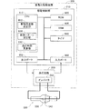
図3は、放電灯駆動装置200の構成を示すブロック図である。放電灯駆動装置200は、駆動制御部210と、点灯回路220とを有している。駆動制御部210は、CPU610と、ROM620と、RAM630と、タイマ640と、点灯回路220に制御信号を出力する出力ポート650と、点灯回路220からの信号を取得する入力ポート660とを備えるコンピュータとして構成されている。駆動制御部210のCPU610は、タイマ640と入力ポート660からの出力信号に基づいて、ROM620に格納されたプログラムを実行する。これにより、CPU610は、駆動周波数設定部612、変調パターン設定部614、および、点灯時間累算部616としての機能を実現する。
FIG. 3 is a block diagram illustrating a configuration of the discharge
点灯回路220は、交流パルス電流を発生するインバータ222を有している。点灯回路220は、駆動制御部210から出力ポート650を介して供給される制御信号に基づいて、インバータ222を制御する。具体的には、点灯回路220は、制御信号により指定された給電条件(例えば、交流パルス電流の周波数やパルス波形)に応じた交流パルス電流をインバータ222に発生させる。インバータ222は、点灯回路220により指定された給電条件に従って、放電灯500に供給する定電力(例えば、200W)の交流パルス電流を発生し、発生した交流パルス電流を放電灯500に供給する。
The
点灯時間累算部616は、放電灯500の使用開始時からの放電灯500の点灯時間(累積点灯時間)を累算する。具体的には、放電灯駆動装置200の電源が投入されると、ROM620の書換可能な領域、あるいは、RAM630の不揮発性の領域から、先に電源が遮断された際の累積点灯時間を取得する。そして、放電灯500を点灯している期間中、タイマ640から供給されるインターバル信号に基づいて累積点灯時間を算出し、放電灯駆動装置200の電源が遮断される際に算出された累積点灯時間をROM620あるいはRAM630に格納する。
The lighting
駆動制御部210の駆動周波数設定部612は、変調パターン設定部614により設定される変調パターンに従って、点灯回路220が出力する交流パルス電流の周波数(駆動周波数)を設定する。このように、駆動周波数は、駆動周波数設定部612と変調パターン設定部614との機能により実現される。そのため、駆動周波数設定部612と変調パターン設定部614は、併せて、「駆動周波数変調部」あるいは単に「周波数変調部」とも呼ぶことができる。変調パターン設定部614は、点灯時間累算部616が算出した放電灯500の累積点灯時間に基づいて、設定する変調パターンを変更する。なお、累積点灯時間に基づく変調パターンの変更の具体的な内容については、後述する。
The drive
A3.放電灯の駆動周波数変調:
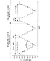
図4は、変調パターン設定部614により設定される駆動周波数fdの変調パターンの一例を示す説明図である。図4(a)は、駆動周波数fdの時間変化を示すグラフである。図4(a)に示す変調パターンでは、駆動周波数fdが4秒毎に50Hzずつ変更されことにより、駆動周波数fdが変調される。駆動周波数fdが一定値に維持される期間(維持期間)を12個設けることにより、駆動周波数fdの変調の周期(変調周期)Tm1は48秒となっており、最も駆動周波数fdが高い期間(最高周波数期間)Th1の駆動周波数fdは350Hzに、最も駆動周波数fdが低い期間(最低周波数期間)Tl1の駆動周波数fdは50Hzに設定されている。
A3. Discharge lamp drive frequency modulation:
FIG. 4 is an explanatory diagram showing an example of a modulation pattern of the drive frequency fd set by the modulation
図4(b)は、図4(a)に示す変調パターンの最低周波数期間Tl1と最高周波数期間Th1とにおいて、放電灯500に供給される電流(ランプ電流)Ipの時間変化を示している。図4(b)において、ランプ電流Ipの正方向は、主鏡側電極532から副鏡側電極542に向かって電流が流れる方向を表している。すなわち、ランプ電流Ipが正の値である期間Tal,Tahでは、主鏡側電極532が陽極として動作し、ランプ電流Ipが負の値である期間Tcl,Tchでは、主鏡側電極532が陰極として動作する。なお、以下では、一方の電極が陽極として動作する期間を当該電極の「陽極期間」とも呼び、一方の電極が陰極として動作する期間を当該電極の「陰極期間」とも呼ぶ。
FIG. 4B shows temporal changes in the current (lamp current) Ip supplied to the
図4(a)に示すように、最高周波数期間Th1における駆動周波数fd(350Hz)は、最低周波数期間Tl1における駆動周波数fd(50Hz)の7倍となっている。そのため、図4(b)に示すように、最低周波数期間Tl1においてランプ電流Ipの極性が切り替えられる切替周期Tplは、最高周波数期間Th1における切替周期Tphの7倍の長さとなっている。また、最低周波数期間Tl1における主鏡側電極532の陽極期間Talと陰極期間Tclとは、それぞれ、最高周波数期間Th1における陽極期間Tahと陰極期間Tchの7倍の長さとなっている。
As shown in FIG. 4A, the drive frequency fd (350 Hz) in the highest frequency period Th1 is seven times the drive frequency fd (50 Hz) in the lowest frequency period Tl1. Therefore, as shown in FIG. 4B, the switching cycle Tpl in which the polarity of the lamp current Ip is switched in the lowest frequency period Tl1 is seven times as long as the switching cycle Tph in the highest frequency period Th1. Further, the anode period Tal and the cathode period Tcl of the primary
第1実施例では、ランプ電流Ipの波形として、矩形波を用いている。このように、ランプ電流Ipを矩形波とすることにより、ランプ電流Ipの絶対値が一定に保たれる。そのため、ランプ電流Ipが変動することによる放電等500の射出光量が時間的に変動することが抑制される。射出光量の時間的な変動を抑制することにより、表示画像上に縞状の明暗が現れる現象(スクロールノイズ)の発生を抑制することができる。
In the first embodiment, a rectangular wave is used as the waveform of the lamp current Ip. Thus, by making the lamp current Ip a rectangular wave, the absolute value of the lamp current Ip is kept constant. For this reason, the amount of light emitted from the
また、第1実施例では、図4(b)に示すように、主鏡側電極532および副鏡側電極542の陽極デューティ比をいずれも50%としている。ここで、主鏡側電極532の陽極デューティ比とは、切り替え周期Tpl(Tph)に対する、主鏡側電極532の陽極期間Tal(Tah)の長さの比率である。また、副鏡側電極542の陽極デューティ比とは、切り替え周期Tpl(Tph)に対する、副鏡側電極542の陽極期間、すなわち主鏡側電極532の陰極期間Tcl(Tch)の長さの比率である。これらの2つの電極532,542の陽極デューティ比を必ずしも同じものとする必要はない。例えば、図2に示すように副反射鏡520を有する放電灯500を用いる場合に、副鏡側電極542から熱が放出されにくくなることを考慮して、副鏡側電極542の陽極デューティ比を50%よりも低くする、すなわち、主鏡側電極532の陽極デューティ比を50%よりも高くすることも可能である。後述するように、電極における熱の発生は当該電極の陽極期間において起きるので、一方の電極の陽極デューティ比が高くなるに従って、当該電極での発熱量が多くなる。そのため、副鏡側電極542の過度な温度上昇を抑制できる点で、熱が放出されにくい副鏡側電極542の陽極デューティ比を50%よりも低くするのがより好ましい。
Further, in the first embodiment, as shown in FIG. 4B, the anode duty ratios of the primary
図5は、図4(a)に示すように異なる駆動周波数fdで放電灯500を駆動することにより、主鏡側電極532の形状が変化する様子を示す説明図である。図5(a)に示すように、電極532,542には、それぞれ、対向する電極に向かって突起538,548が形成されている。図5(b)は、駆動周波数fdが低い場合における主鏡側電極532の状態を示している。図5(c)は、駆動周波数fdが高い場合における主鏡側電極532の状態を示している。
FIG. 5 is an explanatory diagram showing how the shape of the primary
図5(a)は、主鏡側電極532の陽極期間における2つの電極532,542の状態を示している。図5(a)に示すように、主鏡側電極532の陽極期間では、電子が副鏡側電極542から放出され、主鏡側電極532に衝突する。陽極となっている主鏡側電極532では、衝突した電子の運動エネルギが熱エネルギに変換されるため温度が上昇する。一方、陰極となっている副鏡側電極542では、電子の衝突が起こらないため、熱伝導や放射等により温度が低下する。同様に、副鏡側電極542の陽極期間(すなわち、主鏡側電極532の陰極期間)においては、副鏡側電極542の温度が上昇し、主鏡側電極532の温度が低下する。
FIG. 5A shows the state of the two
主鏡側電極532の陽極期間において、主鏡側電極532の温度が上昇することにより、主鏡側電極532の突起538には、電極材が溶融した溶融部が発生する。そして、主鏡側電極532の陰極期間になると、主鏡側電極532の温度が低下し、突起538の先端部に生じた溶融部の固化が始まる。このように、突起538,548に溶融部が発生し、発生した溶融部が固化することにより、突起538,548は、対向電極に向かって凸の形状に維持される。
During the anode period of the primary
図5(b)および図5(c)は、突起の形状に対して駆動周波数fdが及ぼす影響を示している。駆動周波数fdが低い場合、陽極状態の主鏡側電極532の突起538aは、広い範囲にわたって温度が上昇する。また、駆動周波数fdが低い場合には、対向する副鏡側電極542との電位差により溶融部MRaに加わる力も、溶融部MRaの広い範囲に対して加わる。そのため、図5(b)に示すように、陽極状態の主鏡側電極532の突起538には、扁平な溶融部MRaが形成される。そして、主鏡側電極532が陰極状態になると、溶融部MRaが固化して、扁平な形状の突起538aが形成される。
FIG. 5B and FIG. 5C show the influence of the driving frequency fd on the shape of the protrusion. When the drive frequency fd is low, the temperature of the
一方、駆動周波数fdが高い場合、陽極状態の主鏡側電極532の突起538bにおいて温度が上昇する範囲は小さくなり、突起538bには駆動周波数fdが低い場合よりも小さい溶融部MRbが形成される。また、突起538bの溶融部MRbに加わる力は、溶融部MRbの中心部に集中する。そのため、図5(c)に示すように、突起538に形成された溶融部MRbは、対向する副鏡側電極542に向かって細長くなり、陰極期間において溶融部MRbが固化した突起538bの形状は細長くなる。
On the other hand, when the drive frequency fd is high, the temperature rise range is small in the
このように、駆動周波数fdが低い場合、突起538aが十分に溶融されることにより、突起538aは大きくなる。一方、駆動周波数fdが高い場合、対向する電極に向かうように突起538bの伸長が促進される。そのため、駆動周波数fdを変調することにより、駆動周波数fdが低い低周波駆動時に突起538aが大きくなり、駆動周波数fdが高い高周波駆動時に突起538bが伸長する。これにより、電極532,542の間の距離が増大することが抑制され、放電灯500に定電力の交流パルス電流を供給する際の電極532,542間の電圧(ランプ電圧)の上昇が抑制される。
Thus, when the driving frequency fd is low, the
また、図4(a)に示すように、駆動周波数fdは、最低周波数期間Tl1の50Hzから最高周波数期間Th1の350Hzまで段階的に変化している。そのため、突起538aが大きくなった後、大きくなった突起538aが細長い形状へ順次変化することにより、円錐状等、アークの発生位置を安定化させるのに好ましい形状の突起が形成される。なお、図4に示すような変調パターンにより逐次周波数を変動させた場合、上述したような駆動周波数fdが高い場合の現象と低い場合の現象が連続的に繰り返されるため、見た目には電極532,542の先端の突起538,548が、円錐状等、アークの発生位置を安定化させるのに好ましい形状が維持されているようにみえ、低周波駆動時に突起538aが大きくなり、高周波駆動時に突起538bが伸長する現状を観察するのは難しい。
Further, as shown in FIG. 4A, the drive frequency fd changes stepwise from 50 Hz in the lowest frequency period Tl1 to 350 Hz in the highest frequency period Th1. Therefore, after the
なお、高周波駆動時には、突起538bの形状が細長くなっていくため、突起538bの微小化が進み、微小突起が形成される可能性がある。微小突起が形成されると、微小突起の変形や微小突起の複数化等によりアークの発生位置が移動するフリッカ(アークジャンプ)が発生するおそれがある。しかしながら、第1実施例では、駆動周波数fdを変調することにより、低周波駆動時に微小突起が消滅する。そのため、微小突起の形成が原因となるフリッカは、速やかに解消される。一方、低周波駆動時には、突起538aの形状が扁平化していくため、時間の経過とともにフリッカが発生する可能性が高くなる。図6は、このように、低周波駆動時において、時間の経過がアークの発生状態に与える影響を示す説明図である。
Note that during high frequency driving, since the shape of the
図6(a)は、駆動周波数fdが高い状態から低い状態に切り替えられたとき(低周波駆動開始時)におけるアークARの発生状態を示している。図6(b)は、低周波駆動を開始してから時間が経過したとき(低周波駆動継続時)におけるアークARの発生状態を示している。 FIG. 6A shows a state in which the arc AR is generated when the drive frequency fd is switched from a high state to a low state (at the start of low-frequency drive). FIG. 6B shows the state of occurrence of the arc AR when time has elapsed since the start of the low frequency drive (when the low frequency drive is continued).
上述のように、駆動周波数fdが高い場合には、陽極状態の突起538bにおいて温度が上昇する範囲が小さくなり、細長い突起538bが形成される。そのため、図6(a)に示すように、低周波駆動開始時においては、温度の高い領域HRa(ホットスポット)は突起の先端に形成され、突起538aは対向する副鏡側電極542(図4)側に伸びている。アークARは、電極532の陰極期間において電子e-が放出される位置から発生する。陰極からの電子e-は、温度が高いほど、また、電界が強いほど放出されやすい。そのため、図6(a)に示すように、電子e-は突起538aの先端から放出され、アークARは突起538aの先端から発生する。
As described above, when the drive frequency fd is high, the temperature rising range of the
一方、低周波駆動時には、上述のように、温度が上昇する範囲が広がる。そのため、図6(b)に示すように、低周波駆動継続時においては、ホットスポットHRcが広がる。また、低周波駆動により突起538cが扁平化することにより、突起538cの先端は平坦化する。このように、ホットスポットHRcが広がり、突起538cの先端が平坦化することにより、電子e-が放出されやすい位置が広い範囲に分散する。このため、低周波駆動継続時には、平坦化した突起538cのランダムな位置からアークARが生成され、フリッカが発生する可能性が高くなる。 On the other hand, at the time of low frequency driving, as described above, the range in which the temperature rises widens. Therefore, as shown in FIG. 6B, the hot spot HRc is widened when the low frequency driving is continued. Further, the protrusion 538c is flattened by low frequency driving, so that the tip of the protrusion 538c is flattened. As described above, the hot spot HRc spreads and the tip of the protrusion 538c is flattened, so that the positions where electrons e − are likely to be emitted are dispersed in a wide range. For this reason, when the low frequency driving is continued, the arc AR is generated from a random position of the flattened protrusion 538c, and the possibility of occurrence of flicker increases.
また、放電灯500は、累積点灯時間が長くなるに伴い、電極532,542が消耗し、その先端が平坦化する。そのため、累積点灯時間が長い状態で、低周波駆動の時間を長くすると、フリッカが発生する可能性が高くなる。そこで、第1実施例では、フリッカの発生を抑制するため、累積点灯時間に基づいて、駆動周波数fdの変調パターンを変更している。
Further, as the cumulative lighting time becomes longer, the
A4.変調パターンの変更:
図7は、第1実施例において変調パターンが変更される様子を示す説明図である。なお、変調パターンの変更は、変調パターン設定部614の機能として実現されている。変調パターン設定部614(図3)は、予めROM620に格納された複数の変調パターンから設定する変調パターンを選択するものとしてもよく、また、ROM620に格納された変調パターンの複製をRAM630上に生成し、生成した変調パターンを変更するものとしてもよい。
A4. Modulation pattern change:
FIG. 7 is an explanatory diagram showing how the modulation pattern is changed in the first embodiment. The change of the modulation pattern is realized as a function of the modulation
図7のグラフは、累積点灯時間が所定の時間(図7の例では、500時間)を超える前後における駆動周波数fdの時間変化を示している。図7に示すように、駆動周波数fdの変調パターンは、累積点灯時間が500時間を超える前後で変更されている。なお、図7の例では、変調パターンの変更は、駆動周波数fdが200Hzから250Hzに切り替えられる際に行われているが、変調パターンの変更は任意の時点において行うことが可能である。但し、駆動周波数fdが切り替えられる際に変調パターンを変更するのが好ましい。このように、第1実施例では、累積点灯時間が所定の時間となったときに変調パターンが変更されるので、累積点灯時間が所定の時間以下の時点を「変更前」ともよび、累積点灯時間が所定の時間を超えている時点を「変更後」とも呼ぶ。 The graph of FIG. 7 shows the time change of the drive frequency fd before and after the cumulative lighting time exceeds a predetermined time (500 hours in the example of FIG. 7). As shown in FIG. 7, the modulation pattern of the drive frequency fd is changed before and after the cumulative lighting time exceeds 500 hours. In the example of FIG. 7, the modulation pattern is changed when the drive frequency fd is switched from 200 Hz to 250 Hz. However, the modulation pattern can be changed at an arbitrary time. However, it is preferable to change the modulation pattern when the drive frequency fd is switched. As described above, in the first embodiment, the modulation pattern is changed when the cumulative lighting time reaches a predetermined time. Therefore, the time point when the cumulative lighting time is equal to or shorter than the predetermined time is also referred to as “before change”. The time point when the time exceeds the predetermined time is also referred to as “after change”.
図7において、変更前の変調パターンは、図4(a)と同じである。そして、累積点灯時間が500時間を超えると、駆動周波数fdが一定に保たれる維持期間の長さ(ステップ時間)が、駆動周波数fdによらず、一律に変更前の1/2の2秒に変更される。この変更後の変調パターンでは、最低周波数期間Tl2および最高周波数期間Th2における駆動周波数fd(50Hzと350Hz)と、駆動周波数fdの変更幅(50Hz)とは、いずれも変調パターンの変更前と同じになっている。そのため、変更後の変調パターンにおける変調周期Tm2(24秒)は、変更前の変調パターンにおける変調周期Tm1(48秒)の1/2となっている。なお、以下では、変更後の変調パターンのように、維持期間が短縮されている変調パターンを「短縮パターン」とも呼び、維持期間が短縮されていない変更前の変調パターンを「定常パターン」とも呼ぶ。 In FIG. 7, the modulation pattern before the change is the same as that in FIG. When the cumulative lighting time exceeds 500 hours, the length of the sustain period (step time) during which the drive frequency fd is kept constant is uniformly 1/2 seconds before the change regardless of the drive frequency fd. Changed to In the modulation pattern after this change, the drive frequency fd (50 Hz and 350 Hz) in the lowest frequency period Tl2 and the highest frequency period Th2 and the change width (50 Hz) of the drive frequency fd are both the same as before the change of the modulation pattern. It has become. Therefore, the modulation period Tm2 (24 seconds) in the modulation pattern after the change is ½ of the modulation period Tm1 (48 seconds) in the modulation pattern before the change. In the following, a modulation pattern in which the sustain period is shortened, such as the modified modulation pattern, is also referred to as a “shortened pattern”, and a modulation pattern before the change in which the sustain period is not shortened is also referred to as a “steady pattern”. .
上述のように、第1実施例では、累積点灯時間が所定の時間を超えた場合、各維持期間の長さが、変更前の維持期間よりも短くなっている。そのため、低周波駆動が行われる時間が短縮され、フリッカの発生を抑制することができる。なお、第1実施例では、変更後の維持期間の長さを変更前の維持期間の1/2としているが、一般的には、変更前よりも短くなっていればよい。変更後の維持期間の長さをどの程度変更前よりも短縮するかについては、実験等により適宜決定される。 As described above, in the first embodiment, when the cumulative lighting time exceeds a predetermined time, the length of each sustain period is shorter than the sustain period before the change. Therefore, the time during which low frequency driving is performed is shortened, and flicker generation can be suppressed. In the first embodiment, the length of the maintenance period after the change is set to ½ of the maintenance period before the change, but in general, it may be shorter than that before the change. About how much the length of the maintenance period after the change is shorter than before the change is appropriately determined by experiments or the like.
第1実施例では、駆動周波数fdの変調パターンの変更を累積点灯時間に基づいて行っているが、一般的には、電極532,542が消耗した状態等、放電灯500の劣化状態に基づいて変調パターンを変更するものとしてもよい。放電灯500の劣化状態は、累積点灯時間のほか、ランプ電圧や、放電空間512(図2)の内壁に電極材が蒸着することによる光量の低下等に基づいて検出することも可能である。ランプ電圧は、点灯回路220を適宜構成することにより検出することができる。また、光量の低下は、放電灯500からの射出光の光路中に受光素子を設けることにより検出することができる。
In the first embodiment, the modulation pattern of the drive frequency fd is changed based on the cumulative lighting time. In general, however, based on the deterioration state of the
B.第2実施例:
図8は、第2実施例において変調パターンが変更される様子を示す説明図である。第2実施例は、変更前後の変調パターン、すなわち、定常パターンと短縮パターンとが第1実施例と異なっている。他の点は、第1実施例と同じである。
B. Second embodiment:
FIG. 8 is an explanatory diagram showing how the modulation pattern is changed in the second embodiment. The second embodiment is different from the first embodiment in the modulation pattern before and after the change, that is, the steady pattern and the shortening pattern. The other points are the same as in the first embodiment.
図8に示すように、第2実施例の定常パターンでは、駆動周波数fdが一定に保たれる維持期間は、駆動周波数fdによらず6秒となっている。また、第2実施例の定常パターンでは、最低周波数期間Tl3における駆動周波数fdは100Hzに設定され、最高周波数期間Th3における駆動周波数fdは300Hzに設定されている。駆動周波数fdの変更幅は、第1実施例と同様に50Hzとなっている。そのため、第2実施例の定常パターンにおける変調周期Tm3は48秒となっている。 As shown in FIG. 8, in the steady pattern of the second embodiment, the sustain period during which the drive frequency fd is kept constant is 6 seconds regardless of the drive frequency fd. In the steady pattern of the second embodiment, the drive frequency fd in the lowest frequency period Tl3 is set to 100 Hz, and the drive frequency fd in the highest frequency period Th3 is set to 300 Hz. The change width of the drive frequency fd is 50 Hz as in the first embodiment. Therefore, the modulation period Tm3 in the steady pattern of the second embodiment is 48 seconds.
一方、第2実施例の短縮パターンでは、維持期間は、最高周波数期間Th4の6秒から、最低周波数期間Tl4の2秒まで、駆動周波数fdが低くなるにつれて1秒ずつ短縮されている。最低周波数期間Tl4および最高周波数期間Th4における駆動周波数fd(100Hzと300Hz)と、駆動周波数fdの変更幅(50Hz)とは、いずれも定常パターンと同じである。そのため、第2実施例の短縮パターンにおいては、変調周期Tm4が32秒となっている。なお、第2実施例の短縮パターンでは、駆動周波数fdが50Hz下がるごとに維持期間が1秒ずつ短縮されているが、維持期間の短縮量は必ずしも同一でなくても良く、駆動周波数fd毎に適宜設定される。 On the other hand, in the shortened pattern of the second embodiment, the sustain period is shortened by 1 second as the drive frequency fd decreases from 6 seconds in the highest frequency period Th4 to 2 seconds in the lowest frequency period Tl4. The driving frequency fd (100 Hz and 300 Hz) in the lowest frequency period Tl4 and the highest frequency period Th4 and the change width (50 Hz) of the driving frequency fd are both the same as the steady pattern. Therefore, in the shortened pattern of the second embodiment, the modulation period Tm4 is 32 seconds. In the shortened pattern of the second embodiment, the sustain period is shortened by 1 second every time the drive frequency fd decreases by 50 Hz. However, the amount of shortening of the sustain period does not necessarily have to be the same, and for each drive frequency fd Set as appropriate.
このように、第2実施例では、累積点灯時間が所定の時間を超えた場合、駆動周波数の変調パターンは、駆動周波数fdが下がるに伴い維持期間の長さが短くなる短縮パターンに設定される。これにより、低周波駆動が行われる時間が短縮され、フリッカの発生を抑制することが可能となる。また、第2実施例によれば、高周波駆動が行われる時間を十分長くすることができる。そのため、図5(c)に示すように高周波駆動時における突起538bの伸長が十分行われるので、電極532,542間の距離が増大してランプ電圧が上昇することを抑制することができる。
Thus, in the second embodiment, when the cumulative lighting time exceeds a predetermined time, the modulation pattern of the drive frequency is set to a shortened pattern in which the length of the sustain period is shortened as the drive frequency fd is decreased. . As a result, the time during which low-frequency driving is performed is shortened, and the occurrence of flicker can be suppressed. Further, according to the second embodiment, the time during which high frequency driving is performed can be made sufficiently long. Therefore, as shown in FIG. 5C, the
なお、第2実施例では、駆動周波数fdが低くなるほど維持期間が短くなっているが、一般的には、ある駆動周波数の維持期間の長さが、当該駆動周波数よりも高い駆動周波数の維持期間よりも短ければよい。このようにしても、低周波駆動が行われる時間を短縮するとともに、高周波駆動が行われる時間を十分長くすることができる。また、第2実施例では、定常パターンの最高周波数期間Th3と短縮パターンの最高周波数期間Th4との長さを同じにしているが、必ずしも、これらの期間Th3,Th4の長さが同じでなくても良い。短縮パターンにおける所定の周波数以下の維持期間が、定常パターンにおける当該所定の周波数の以下の維持期間よりも短ければ、短縮パターンの最高周波数期間Th4が定常パターンの最高周波数期間Th3より長くても良く、定常パターンの最高周波数期間Th3が短縮パターンの最高周波数期間Th4より長くても良い。 In the second embodiment, the sustain period is shorter as the drive frequency fd is lower. In general, the sustain period of a certain drive frequency is higher than the drive frequency. Shorter than that. Even in this case, it is possible to shorten the time during which low-frequency driving is performed and sufficiently increase the time during which high-frequency driving is performed. In the second embodiment, the maximum frequency period Th3 of the steady pattern and the maximum frequency period Th4 of the shortening pattern are the same. However, the lengths of the periods Th3 and Th4 are not necessarily the same. Also good. If the sustain period below the predetermined frequency in the shortened pattern is shorter than the sustain period below the predetermined frequency in the stationary pattern, the maximum frequency period Th4 of the shortened pattern may be longer than the maximum frequency period Th3 of the stationary pattern, The maximum frequency period Th3 of the steady pattern may be longer than the maximum frequency period Th4 of the shortened pattern.
C.第3実施例:
図9は、第3実施例における放電灯駆動装置200aの構成を示すブロック図である。第3実施例の放電灯駆動装置200aは、放電灯500に近接して設けられたフリッカセンサ700を有している点と、駆動制御部210aにフリッカセンサ700からの出力信号が供給されるセンサインタフェース670が設けられている点と、CPU610aが点灯時間累算部616に換えてフリッカ検出処理部618としての機能を実現している点とで、第1実施例の放電灯駆動装置200(図3)と異なっている。また、変調パターン設定部614aは、フリッカ検出処理部618が検出したフリッカの発生状態に基づいて変調パターンを変更する点で、第1実施例の変調パターン設定部614と異なっている。他の点は、第1実施例と同様である。
C. Third embodiment:
FIG. 9 is a block diagram showing a configuration of a discharge
フリッカセンサ700は、放電灯500において発生するアークAR(図2)の位置の変化を検出する。第3実施例のフリッカセンサ700は、フォトダイオードやフォトトランジスタなどの受光素子と、アークの発生位置が変化した場合に受光素子に入射する光量を変化させるためのスリットやピンホールにより構成することができる。但し、フリッカセンサ700の構成は、アークの発生位置の変動が検出可能であれば、適宜変更することができる。例えば、アークの位置の変化を検出するフリッカセンサ700として、電荷結合素子(CCD)等で構成されたラインセンサやエリアセンサ等を用いることもできる。
フリッカ検出処理部618は、センサインタフェース670を介して取得したフリッカセンサ700の出力信号を解析して、放電灯500におけるフリッカの発生状態を検出する。フリッカの発生状態は、例えば、フリッカセンサ700が有する受光素子への入射光量の変動量に基づいて検出することができる。この場合、変動量が所定の基準値を超えた場合にフリッカが発生したと判断される。なお、フリッカ検出処理部618におけるフリッカの検出は、フリッカセンサ700の構成に応じて適宜変更される。
The flicker
図10は、第3実施例の変調パターン設定部614aが、変調パターンを変更する処理の流れを示すフローチャートである。変調パターンの変更処理は、放電灯500が点灯状態である間、繰り返し実行される。
FIG. 10 is a flowchart showing a flow of processing in which the modulation pattern setting unit 614a of the third embodiment changes the modulation pattern. The modulation pattern changing process is repeatedly executed while the
ステップS110において、変調パターン設定部614aは、フリッカの発生状態を取得する。具体的には、フリッカ検出処理部618からフリッカの発生状態を取得する。
In step S110, the modulation pattern setting unit 614a acquires a flicker occurrence state. Specifically, the flicker occurrence state is acquired from the flicker
ステップS120において、変調パターン設定部614aは、駆動周波数が所定の基準周波数(例えば、200Hz)以下の維持期間でフリッカが発生しているか否かを判断する。基準周波数以下の維持期間でフリッカが発生していると判断された場合、処理はステップS130に進む。一方、基準周波数以下の維持期間でフリッカが発生していないと判断された場合、処理はステップS110に戻され、2つのステップS110,S120が繰り返し実行される。 In step S120, the modulation pattern setting unit 614a determines whether or not flicker occurs in a sustain period in which the drive frequency is equal to or lower than a predetermined reference frequency (for example, 200 Hz). If it is determined that flicker has occurred in the sustain period below the reference frequency, the process proceeds to step S130. On the other hand, if it is determined that no flicker occurs in the sustain period below the reference frequency, the process returns to step S110, and the two steps S110 and S120 are repeatedly executed.
ステップS130において、変調パターン設定部614aは、変調パターンを変更することにより、フリッカが発生した周波数以下の維持期間を短縮する。変調パターンの変更は、第1実施例と同様に、駆動周波数fdが200Hzから250Hzに切り替えられる際に行われる。但し、変調パターンの変更は任意の時点において行うことが可能である。 In step S130, the modulation pattern setting unit 614a shortens the sustain period below the frequency at which flicker occurs by changing the modulation pattern. The modulation pattern is changed when the drive frequency fd is switched from 200 Hz to 250 Hz, as in the first embodiment. However, the modulation pattern can be changed at any time.
ステップS140において、変調パターン設定部614aは、変調パターンを変更した後、所定の時間が経過したか否かを判断する。所定の時間が経過したと判断された場合、処理は、ステップS150に進む。一方、所定の時間が経過していないと判断された場合、所定の時間が経過するまでステップS140が繰り返し実行される。なお、所定の時間は、低周波駆動時のフリッカの発生が抑制される程度まで突起の形状が変化するのに要する時間(例えば、10〜20分)に設定される。 In step S140, the modulation pattern setting unit 614a determines whether or not a predetermined time has elapsed after changing the modulation pattern. If it is determined that the predetermined time has elapsed, the process proceeds to step S150. On the other hand, if it is determined that the predetermined time has not elapsed, step S140 is repeatedly executed until the predetermined time has elapsed. The predetermined time is set to a time (for example, 10 to 20 minutes) required for the shape of the protrusion to change to such an extent that the occurrence of flicker during low frequency driving is suppressed.
ステップS150において、変調パターン設定部614aは、ステップS110と同様に、フリッカの発生状態を取得する。そして、ステップS160において、変調パターン設定部614aは、ステップS120で発生していると判断されたフリッカが解消したか否かを判断する。フリッカが解消したと判断された場合、処理はステップS170に進む。一方、フリッカが解消していないと判断された場合、処理はステップS140に戻され、フリッカが解消するまでステップS140〜S160が繰り返し実行される。なお、フリッカが解消したか否かの判断を行う際には、フリッカの解消をより確実に判断するため、短縮された維持期間の長さを一時的に短縮前の長さに戻すのがより好ましい。 In step S150, the modulation pattern setting unit 614a acquires the flicker occurrence state in the same manner as in step S110. In step S160, the modulation pattern setting unit 614a determines whether the flicker determined to have occurred in step S120 has been eliminated. If it is determined that the flicker has been resolved, the process proceeds to step S170. On the other hand, if it is determined that the flicker has not been eliminated, the process returns to step S140, and steps S140 to S160 are repeatedly executed until the flicker is eliminated. When determining whether or not flicker has been resolved, it is better to temporarily return the length of the shortened maintenance period to the length before shortening in order to more reliably determine whether or not flicker has been resolved. preferable.
ステップS170において、変調パターン設定部614aは、ステップS130において短縮した維持期間の長さを元に戻す(以下、「復元」とも呼ぶ)。維持期間の復元は、例えば、駆動周波数設定部612に設定する変調パターンを、ROM620あるいはRAM630に格納されている短縮前の変調パターンに変更することにより行うことができる。ステップS170における維持期間の復元の後、処理はステップS110に戻され、基準周波数以下の維持期間でフリッカが発生するまで、ステップS110,S120が繰り返し実行される。
In step S170, the modulation pattern setting unit 614a restores the length of the sustain period shortened in step S130 (hereinafter also referred to as “restoration”). The sustain period can be restored, for example, by changing the modulation pattern set in the drive
図11は、図10に示す変調パターンの変更処理により変調パターンが変更される様子を示す説明図である。図11における維持期間の短縮前における変調パターン、すなわち定常パターンは、第2実施例と同じである。 FIG. 11 is an explanatory diagram showing how the modulation pattern is changed by the modulation pattern change processing shown in FIG. The modulation pattern before shortening the sustain period in FIG. 11, that is, the steady pattern, is the same as in the second embodiment.
図11の例では、時刻t1より以前においては、フリッカが発生していない。そして、時刻t1〜t2の期間において、フリッカが発生している。そのため、時刻t1から始まる駆動周波数fdが150Hzの維持期間において、フリッカが基準周波数(200Hz)以下で発生したと判断される(ステップS120)。そして、駆動周波数fdが200Hzから250Hzに切り替えられる時刻t3において変調パターンが短縮パターンに変更される(ステップS130)。 In the example of FIG. 11, no flicker occurs before time t1. In the period from time t1 to time t2, flicker occurs. Therefore, it is determined that the flicker has occurred at the reference frequency (200 Hz) or less in the sustain period in which the drive frequency fd starting from time t1 is 150 Hz (step S120). Then, at time t3 when the drive frequency fd is switched from 200 Hz to 250 Hz, the modulation pattern is changed to a shortened pattern (step S130).
図11の例では、駆動周波数fdが150Hzの際にフリッカが発生しているため、短縮パターンでは、駆動周波数fdが150Hzおよび100Hzの維持期間が、定常パターンの1/3の2秒に短縮されている。そのため、短縮パターンにおける変調周期Tm5は、36秒となっている。なお、維持期間の短縮の程度は、適宜変更することが可能である。 In the example of FIG. 11, flicker occurs when the drive frequency fd is 150 Hz. Therefore, in the shortened pattern, the sustain period of the drive frequency fd of 150 Hz and 100 Hz is shortened to 2/3, which is 1/3 of the steady pattern. ing. Therefore, the modulation period Tm5 in the shortened pattern is 36 seconds. Note that the degree of shortening the maintenance period can be changed as appropriate.
このように、第3実施例では、フリッカが発生した周波数以下の維持期間を短縮することにより、低周波駆動が行われる時間が短縮され、フリッカの発生を抑制することが可能となる。また、第3実施例によっても、高周波駆動が行われる時間を十分長くすることができるので、ランプ電圧の上昇を抑制することができる。 Thus, in the third embodiment, by shortening the sustain period below the frequency at which flicker occurs, the time during which low-frequency driving is performed is shortened, and flicker generation can be suppressed. Also, according to the third embodiment, the time during which high-frequency driving is performed can be made sufficiently long, so that an increase in lamp voltage can be suppressed.
第3実施例では、駆動周波数fdがフリッカが発生した周波数以下の全ての維持期間を短縮しているが、フリッカが発生した周波数の維持期間のみを短縮するものとしてもよい。また、基準周波数以下でフリッカが発生した場合、基準周波数以下の維持期間全体を短縮するものとしてもよい。一般的には、フリッカが発生した場合に、基準周波数以下の少なくとも1つの維持期間が短縮されればよく、第1実施例の短縮パターンと同様に、全ての維持期間を短縮しても良く、また、第2実施例の短縮パターンと同様に、駆動周波数が低くなるに従って維持期間を短くするものとしてもよい。 In the third embodiment, all the sustain periods in which the drive frequency fd is equal to or lower than the frequency at which the flicker occurs are shortened, but only the sustain period of the frequency at which the flicker occurs may be shortened. Further, when flicker occurs below the reference frequency, the entire sustain period below the reference frequency may be shortened. In general, when flicker occurs, it is only necessary to shorten at least one sustain period below the reference frequency. Like the shortened pattern of the first embodiment, all sustain periods may be shortened, Further, similarly to the shortened pattern of the second embodiment, the sustain period may be shortened as the drive frequency is lowered.
また、第3実施例では、変調パターンが短縮パターンに変更された後、所定の時間が経過した際にフリッカが解消しているか否かを判断しているが(ステップS140〜S160)、所定の時間の経過を待たず、フリッカが解消しているか否かを判断するものとしてもよい。ただし、所定の時間が経過する間に、細長い突起538b(図5(c))の形成が行われ、維持期間を復元した際のフリッカの再発生が抑制できる点で、所定時間経過後にフリッカの解消を判断するのが好ましい。
In the third embodiment, it is determined whether or not the flicker has been eliminated when a predetermined time has elapsed after the modulation pattern is changed to the shortened pattern (steps S140 to S160). It may be determined whether the flicker has been eliminated without waiting for the passage of time. However, the
第3実施例では、フリッカが解消した場合に短縮された維持期間の長さを復元しているが、維持期間の長さの復元を行わないものとしてもよい。この場合、例えば、放電灯500を消灯されるまで、あるいは、放電灯駆動装置200a電源が遮断されるまで、維持期間を短縮したままとし、放電灯500の点灯開始時、あるいは、放電灯駆動装置200aの電源投入時に維持期間の長さを復元するものとしてもよい。また、維持期間の長さの復元を全く行わないものとしてもよい。但し、維持期間の長さを復元することにより、高周波駆動時に形成されうる微小突起を消滅させ、微小突起の形成によるフリッカの発生を抑制できる点で、フリッカが解消した場合に短縮された維持期間の長さを復元するのがより好ましい。
In the third embodiment, when the flicker is eliminated, the shortened maintenance period length is restored. However, the maintenance period length may not be restored. In this case, for example, the sustain period is kept shortened until the
D.第4実施例:
図12は、第4実施例において変調パターンが変更される様子を示す説明図である。第4実施例は、変更前後の変調パターンが第1実施例と異なっている。他の点は、第1実施例と同じである。
D. Fourth embodiment:
FIG. 12 is an explanatory diagram showing how the modulation pattern is changed in the fourth embodiment. The fourth embodiment differs from the first embodiment in the modulation pattern before and after the change. The other points are the same as in the first embodiment.
図12に示すように、第4実施例の定常パターンでは、駆動周波数fdが一定に保たれる維持期間は、駆動周波数fdによらず4秒となっている。また、この定常パターンでは、最低周波数期間Tl1における駆動周波数fdは50Hzに設定され、最高周波数期間Th1における駆動周波数fdは350Hzに設定されている。駆動周波数fdの変更幅は、第1実施例と同様に50Hzとなっている。そのため、第4実施例の定常パターンにおける変調周期Tm1は48秒となっている。 As shown in FIG. 12, in the steady pattern of the fourth embodiment, the sustain period during which the drive frequency fd is kept constant is 4 seconds regardless of the drive frequency fd. In this steady pattern, the drive frequency fd in the lowest frequency period Tl1 is set to 50 Hz, and the drive frequency fd in the highest frequency period Th1 is set to 350 Hz. The change width of the drive frequency fd is 50 Hz as in the first embodiment. Therefore, the modulation period Tm1 in the steady pattern of the fourth embodiment is 48 seconds.
第4実施例では、累積点灯時間が所定の時間(図12の例では、500時間)を超えた場合には、駆動周波数の変調パターンは、最高周波数期間Th1の長さが、定常パターンの場合と比べて長くなる伸長パターンに設定される。すなわち、最高周波数期間Th3が、定常パターン時の4秒から、伸長パターン時の10秒に変更されている。その上で、駆動周波数fdの変調周期が、駆動周波定常パターンの場合と伸長パターンの場合とで同一となるように、駆動周波数fdが300Hzのときと250Hzのときの各維持期間を2.5秒に変更されている。 In the fourth embodiment, when the cumulative lighting time exceeds a predetermined time (500 hours in the example of FIG. 12), the modulation pattern of the drive frequency is a case where the length of the maximum frequency period Th1 is a steady pattern. The extension pattern is set to be longer than the extension pattern. That is, the maximum frequency period Th3 is changed from 4 seconds in the stationary pattern to 10 seconds in the extended pattern. In addition, each sustain period when the drive frequency fd is 300 Hz and 250 Hz is set to 2.5 so that the modulation period of the drive frequency fd is the same between the case of the drive frequency steady pattern and the case of the extension pattern. Has been changed to seconds.
一般に、電極が劣化して電極の溶融性が低下すると、駆動周波数fdが低い場合に、突起は先端が平坦な熱容量の大きな形状になり、その突起表面に凹凸が形成され、フリッカが発生するおそれが高くなる。これに対して、上記構成の第4実施例では、所定の条件が満たされた場合(第4実施例では、累積点灯時間が所定の時間を超えた場合)に、最高周波数期間Th1を所定の条件が満たされる前と比べて長くなる構成としていることから、最高周波数期間Th1において細い突起が形成し熱容量を減少させることができ、突起表面の溶融性を確保することができる。このため、フリッカの発生を抑制することが可能となる。 In general, when the electrode deteriorates and the meltability of the electrode decreases, when the driving frequency fd is low, the protrusion has a flat tip and a large heat capacity, and the protrusion surface may be uneven and flicker may occur. Becomes higher. On the other hand, in the fourth embodiment having the above configuration, when a predetermined condition is satisfied (in the fourth embodiment, when the cumulative lighting time exceeds a predetermined time), the maximum frequency period Th1 is set to a predetermined value. Since the length is longer than that before the condition is satisfied, a thin protrusion is formed in the maximum frequency period Th1, the heat capacity can be reduced, and the meltability of the protrusion surface can be ensured. For this reason, it is possible to suppress the occurrence of flicker.
E.第5実施例:
図13は、第5実施例において変調パターンが変更される様子を示す説明図である。第5実施例は、変更前後の変調パターンが第2実施例と異なっている。他の点は、第2実施例と同じである。第4実施例では、変更後の変調パターン(伸長パターン)は、最高周波数期間Th3の長さが定常パターンの場合と比べて長くなるように構成されていた。これに対して、この第5実施例では、伸長パターンは、所定の基準周波数を上回る全ての維持期間の長さが、定常パターンの場合と比べて長くなるように構成されている。
E. Example 5:
FIG. 13 is an explanatory diagram showing how the modulation pattern is changed in the fifth embodiment. The fifth embodiment is different from the second embodiment in the modulation pattern before and after the change. The other points are the same as in the second embodiment. In the fourth embodiment, the changed modulation pattern (expansion pattern) is configured such that the length of the maximum frequency period Th3 is longer than that of the steady pattern. On the other hand, in the fifth embodiment, the extension pattern is configured such that the length of all sustain periods exceeding a predetermined reference frequency is longer than that in the case of the steady pattern.
第5実施例では、すなわち、図13に示すように、駆動周波数が所定の基準周波数(例えば、200Hz)を上回る250Hzおよび300Hzのときの各維持期間が、定常パターン時の6秒から、伸長パターン時の10秒に変更されている。駆動周波数が所定の基準周波数以下である場合には、定常パターン時、伸長パターン時ともに6秒で変更がない。 In the fifth embodiment, that is, as shown in FIG. 13, each sustain period when the drive frequency is higher than a predetermined reference frequency (for example, 200 Hz) at 250 Hz and 300 Hz is an extension pattern from 6 seconds in the steady pattern. The time has been changed to 10 seconds. When the drive frequency is equal to or lower than a predetermined reference frequency, there is no change in 6 seconds for both the steady pattern and the extended pattern.
上記構成の第5実施例では、第4実施例と同様に、駆動周波数fdが低い場合に発生する突起表面の凹凸を少なくすることができる。このため、フリッカの発生を抑制することが可能となる。 In the fifth embodiment having the above configuration, as in the fourth embodiment, it is possible to reduce the unevenness of the projection surface that occurs when the drive frequency fd is low. For this reason, it is possible to suppress the occurrence of flicker.
F.変形例:
なお、この発明は上記実施例や実施形態に限られるものではなく、その要旨を逸脱しない範囲において種々の態様において実施することが可能であり、例えば次のような変形も可能である。
F. Variations:
In addition, this invention is not restricted to the said Example and embodiment, It can implement in a various aspect in the range which does not deviate from the summary, For example, the following deformation | transformation is also possible.
F1.変形例1:
上記各実施例に示した変調パターンは、あくまで一例であって、駆動周波数の変調範囲(すなわち、最高周波数期間Th1〜Th5と最低周波数期間Tl1〜Tl5における駆動周波数)、駆動周波数が一定に保たれる維持期間の数、維持期間の長さ、駆動周波数の変化量等は、放電灯500の特性などによって適宜変更される。一般に、駆動周波数の変調は、変調周期内に駆動周波数が互いに異なる複数の期間を設けることにより行われればよい。例えば、維持期間の長さが駆動周波数ごとに異なっていても良く、また、駆動周波数が段階的に切り替えられないものとしてもよい。このようにしても、所定の周波数以下の維持期間を短縮することにより、低周波駆動時におけるフリッカの発生を抑制することができる。また、所定の条件が満たされた場合に、最低周波数期間だけを、所定の条件が満たされる前と比べて短縮する構成としてもよい。
F1. Modification 1:
The modulation patterns shown in the above embodiments are merely examples, and the modulation range of the drive frequency (that is, the drive frequency in the highest frequency period Th1 to Th5 and the lowest frequency period Tl1 to Tl5) and the drive frequency are kept constant. The number of sustain periods, the length of the sustain period, the amount of change in drive frequency, and the like are appropriately changed according to the characteristics of the
F2.変形例2:
前記第1ないし第3実施例では、所定の基準周波数以下である少なくとも一期間を短縮する構成とし、第4実施例では、所定の基準周波数を上回る少なくとも一期間を伸長する構成としたが、上記「所定の基準周波数」は、200Hzに限る必要はなく、フリッカが発生し易い周波数であれば、放電灯500の特性などによって適宜変更され得る。さらに、期間を短縮する第1ないし第3実施例における「所定の基準周波数」と、期間を伸長する第4実施例における「所定の基準周波数」とは、同一である必要はなく個別の値でもよい。
F2. Modification 2:
In the first to third embodiments, at least one period that is equal to or lower than a predetermined reference frequency is shortened. In the fourth embodiment, at least one period that exceeds a predetermined reference frequency is extended. The “predetermined reference frequency” does not have to be limited to 200 Hz, and can be appropriately changed depending on the characteristics of the
F3.変形例3:
上記各実施例では、放電灯500の劣化状態や実際のフリッカの発生に基づいて、変調パターンを定常パターンから短縮パターンに切り替えているが、他の条件に基づいて変調パターンを切り替えることも可能である。例えば、放電灯駆動装置200が、放電灯500の定格電力よりも低い電力で放電灯500を駆動することが可能に構成されている場合、定格電力で駆動している際には定常パターンを用い、定格電力よりも低い電力(低電力)で駆動している際には短縮パターンを用いるものとしてもよい。なお、変調パターンの切替の基準となる電力は、必ずしも定格電力に限らない。一般に、放電灯の駆動電力が所定の基準電力以上の場合に定常パターンを用い、所定の基準電力よりも小さい場合に短縮パターンを用いるものとしてもよい。
F3. Modification 3:
In each of the above embodiments, the modulation pattern is switched from the steady pattern to the shortened pattern based on the deterioration state of the
図14は、低電力駆動時において、低周波駆動を継続した場合のアークARの発生状態を示す説明図である。図14(a)は、低周波駆動開始時におけるアークARの発生状態を示し、図14(b)は、低周波駆動継続時におけるアークARの発生状態を示している。 FIG. 14 is an explanatory diagram showing a state in which an arc AR is generated when low frequency driving is continued during low power driving. FIG. 14A shows the state of occurrence of the arc AR at the start of the low frequency drive, and FIG. 14B shows the state of occurrence of the arc AR when the low frequency drive is continued.
上述のように、駆動周波数fdが高い場合には、陽極状態の突起538dにおいて温度が上昇する範囲が小さくなる。そのため、低電力駆動中においても、図14(a)に示すように、低周波駆動開始時には、温度が十分高いホットスポットHRdが突起の先端に形成されている。このように、低周波駆動開始時には、ホットスポットHRdが突起538dに形成されているので、アークARは、ホットスポットHRdの位置、すなわち、突起538dの先端から発生する。
As described above, when the drive frequency fd is high, the range in which the temperature rises in the anode-shaped
一方、電極532全体の温度が低下する低電力駆動中において低周波駆動を継続すると、温度が上昇する範囲が低周波駆動により広がるため、突起538dの先端の温度が十分に上昇しない。そのため、低周波駆動継続時には、図14(b)に示すように、突起538dの先端の温度が十分に上昇しなくなり、低周波駆動開始時に形成されていたホットスポットHRdが消滅する。このように、温度が十分に高いホットスポットHRdが消滅すると、電子e-が放出されやすい位置が定まらなくなり、突起538dのランダムな位置からアークARが生成されるため、フリッカが発生する可能性が高くなる。
On the other hand, if the low frequency driving is continued during the low power driving in which the temperature of the
このように、変調パターンとして、定格電力駆動時には定常パターンを用い、低電力駆動時には短縮パターンを用いることにより、低電力駆動中におけるフリッカの発生を抑制することが可能となる。 Thus, by using a steady pattern as the modulation pattern at the rated power drive and using a shortened pattern at the low power drive, it is possible to suppress the occurrence of flicker during the low power drive.
なお、変調パターンの切替を、単一の条件でなく、複数の条件に基づいて行うことも可能である。例えば、定格電力駆動時においては、放電灯500の劣化状態やフリッカの発生に基づいて変調パターンの切替を行い、低電力駆動時には、放電灯500の劣化状態やフリッカの発生の有無にかかわらず短縮パターンを用いるものとしてもよい。また、放電灯500の劣化状態に基づいて変調パターンを切り替える際の基準を、定格電力駆動時と、低電力駆動時とにおいて変更するものとしてもよい。
Note that modulation pattern switching can be performed based on a plurality of conditions instead of a single condition. For example, when driving at rated power, the modulation pattern is switched based on the deterioration state of the
F4.変形例4:
図15は、放電灯に備えられる電極についての変形例を上記実施例と比較して示す説明図である。図15(a)は上記各実施例における電極532(542)の形状を示すものであり、図15(b)は変形例4における電極の形状を示すものである。図15(a)に示すように、上記各実施例における電極532(542)の先端は球面となっている。球面形状となっていることは、先に説明した図5および図6にも示した。このように、上記各実施例では、電極の先端を球面形状とすることで、劣化時の変化を修復する効果をより大きくすることが可能となっている。
F4. Modification 4:
FIG. 15 is an explanatory view showing a modification of the electrode provided in the discharge lamp in comparison with the above-described embodiment. FIG. 15A shows the shape of the electrode 532 (542) in each of the above embodiments, and FIG. 15B shows the shape of the electrode in Modification 4. As shown in FIG. 15A, the tip of the electrode 532 (542) in each of the above embodiments is a spherical surface. The spherical shape is also shown in FIGS. 5 and 6 described above. As described above, in each of the above embodiments, it is possible to increase the effect of repairing the change at the time of deterioration by making the tip of the electrode spherical.
これに対して、図15(b)は、電極1532の先端は円錐形状となっている。これによっても、上記各実施例と同様にフリッカの発生を抑制することができる。すなわち、電極1532の先端は、必ずしも球面形状である必要もなく、円錐形状等の種々の形状とすることができる。
On the other hand, in FIG. 15B, the tip of the
F5.変形例5:
上記各実施例では、プロジェクタ1000(図1)における光変調手段として、液晶ライトバルブ330R,330G,330Bを用いているが、光変調手段としては、DMD(デジタルマイクロミラーデバイス:Texas Instruments社の商標)など、他の任意の変調手段を用いることも可能である。また、本発明は、放電灯を光源とする装置であれば、液晶表示装置をはじめとする種々の画像表示装置や、露光装置や照明装置等に適用することもできる。
F5. Modification 5:
In each of the above embodiments, the liquid crystal
100…光源装置
110…光源ユニット
112…主反射鏡
114…平行化レンズ
116…無機接着剤
200,200a…放電灯駆動装置
210,210a…駆動制御部
220…点灯回路
310…照明光学系
320…色分離光学系
330R,330G,330B…液晶ライトバルブ
340…クロスダイクロイックプリズム
350…投写光学系
500…放電灯
510…放電灯本体
512…放電空間
520…副反射鏡
522…無機接着剤
532,542…電極
534,544…接続部材
536,546…電極端子
538,538a,538b,538c,538d…突起
548…突起
610…CPU
612…駆動周波数設定部
614,614a…変調パターン設定部
616…点灯時間累算部
618…フリッカ検出処理部
620…ROM
630…RAM
640…タイマ
650…出力ポート
660…入力ポート
670…センサインタフェース
700…フリッカセンサ
1000…プロジェクタ
MRa,MRb…溶融部
HRa,HRc,HRd…ホットスポット
DESCRIPTION OF
612: Driving
630 ... RAM
640 ...
Claims (10)
前記放電灯の2つの電極間に交流電流を供給する交流電流供給部と、
変調の一周期内において、前記交流電流の周波数が互いに異なる複数の期間を設けることにより前記周波数を変調する周波数変調部と
を備え、
前記周波数変調部は、所定の条件が満たされた場合に、前記複数の期間のうちの、前記周波数が所定の基準周波数以下である少なくとも一期間を、前記所定の条件が満たされる前と比べて短縮し、
前記周波数変調部は、前記短縮を行う際に、前記複数の期間のうち、前記周波数が第1の周波数である第1の期間の長さを、前記周波数が前記第1の周波数よりも高い第2の周波数である第2の期間よりも短くし、
前記周波数変調部は、前記短縮を行う際に、前記周波数が低くなるに従って当該周波数の期間を短くする
放電灯の駆動装置。 A discharge lamp driving device comprising:
An alternating current supply unit for supplying an alternating current between two electrodes of the discharge lamp;
A frequency modulation unit that modulates the frequency by providing a plurality of periods in which the frequency of the alternating current is different from each other within one period of modulation, and
When the predetermined condition is satisfied, the frequency modulation unit compares at least one period in which the frequency is equal to or lower than a predetermined reference frequency among the plurality of periods compared to before the predetermined condition is satisfied. Shortened ,
The frequency modulation unit, when performing the shortening, sets the length of the first period in which the frequency is the first frequency among the plurality of periods, and the frequency is higher than the first frequency. Shorter than the second period, which is a frequency of 2 ,
The frequency modulation unit shortens the period of the frequency as the frequency becomes lower when performing the shortening.
前記周波数変調部は、前記所定の条件が満たされた場合に、前記複数の期間のそれぞれを短縮する
放電灯の駆動装置。 A driving device for a discharge lamp of claim 1 Symbol placement,
The frequency modulation unit shortens each of the plurality of periods when the predetermined condition is satisfied.
前記所定の条件の判断基準として前記放電灯におけるフリッカの発生を検出するフリッカ検出部を備え、
前記周波数変調部は、前記周波数が前記基準周波数以下である期間においてフリッカが検出された場合に前記短縮を行う
放電灯の駆動装置。 The driving device for a discharge lamp according to claim 1 or 2, further comprising:
A flicker detection unit for detecting occurrence of flicker in the discharge lamp as a determination criterion for the predetermined condition;
The frequency modulation unit performs the shortening when flicker is detected in a period in which the frequency is equal to or lower than the reference frequency.
前記周波数変調部は、前記短縮から所定の時間が経過した後、前記フリッカが検出された周波数においてフリッカが発生しているか否かを判断し、フリッカが発生していない場合には、前記短縮された期間を短縮前の長さに復元する
放電灯の駆動装置。 A discharge lamp driving device according to claim 3 ,
The frequency modulation unit determines whether or not flicker has occurred at a frequency at which the flicker has been detected after a predetermined time has elapsed since the shortening. A discharge lamp drive device that restores the previous period to the length before shortening.
前記所定の条件は、前記放電灯の劣化状態に基づいて判断され、
前記周波数変調部は、前記放電灯の劣化が進行していると判断された場合に前記短縮を行う
放電灯の駆動装置。 A discharge lamp driving device according to claim 1 or 2 ,
The predetermined condition is determined based on a deterioration state of the discharge lamp,
The frequency modulation unit performs the shortening when it is determined that the deterioration of the discharge lamp is progressing.
前記劣化状態を表すパラメータとして前記放電灯の使用開始からの累積点灯時間を算出する点灯時間累算部を備え、
前記周波数変調部は、前記累積点灯時間が所定の上限時間を超えた場合に、前記短縮を行う
放電灯の駆動装置。 The discharge lamp driving device according to claim 5 , further comprising:
A lighting time accumulation unit that calculates a cumulative lighting time from the start of use of the discharge lamp as a parameter representing the deterioration state,
The frequency modulation unit performs the shortening when the accumulated lighting time exceeds a predetermined upper limit time.
前記交流電流供給部は、前記放電灯に供給する前記交流電流の電力を変更可能に構成されており、
前記周波数変調部は、前記放電灯に供給される前記交流電流の電力が所定の基準電力より低い場合には、前記短縮を行う
放電灯の駆動装置。 The discharge lamp driving device according to any one of claims 1 to 6 ,
The alternating current supply unit is configured to be able to change the power of the alternating current supplied to the discharge lamp,
The frequency modulation unit performs the shortening when the power of the alternating current supplied to the discharge lamp is lower than a predetermined reference power.
放電灯と、
前記放電灯を点灯するために、前記放電灯の2つの電極間に交流電流を供給する交流電流供給部と、
変調の一周期内において、前記交流電流の周波数が互いに異なる複数の期間を設けることにより前記周波数を変調する周波数変調部と
を備え、
前記周波数変調部は、所定の条件が満たされた場合に、前記複数の期間のうちの、前記周波数が所定の基準周波数以下である少なくとも一期間を、前記所定の条件が満たされる前と比べて短縮し、
前記周波数変調部は、前記短縮を行う際に、前記複数の期間のうち、前記周波数が第1の周波数である第1の期間の長さを、前記周波数が前記第1の周波数よりも高い第2の周波数である第2の期間よりも短くし、
前記周波数変調部は、前記短縮を行う際に、前記周波数が低くなるに従って当該周波数の期間を短くする
光源装置。 A light source device,
A discharge lamp,
An alternating current supply unit for supplying an alternating current between two electrodes of the discharge lamp to turn on the discharge lamp;
A frequency modulation unit that modulates the frequency by providing a plurality of periods in which the frequency of the alternating current is different from each other within one period of modulation, and
When the predetermined condition is satisfied, the frequency modulation unit compares at least one period in which the frequency is equal to or lower than a predetermined reference frequency among the plurality of periods compared to before the predetermined condition is satisfied. Shortened ,
The frequency modulation unit, when performing the shortening, sets the length of the first period in which the frequency is the first frequency among the plurality of periods, and the frequency is higher than the first frequency. Shorter than the second period, which is a frequency of 2,
The frequency modulation unit, when performing the shortening, is a light source device that shortens the period of the frequency as the frequency becomes lower .
画像表示用の光源である放電灯と、
前記放電灯を点灯するために、前記放電灯の2つの電極間に交流電流を供給する交流電流供給部と、
変調の一周期内において、前記交流電流の周波数が互いに異なる複数の期間を設けることにより前記周波数を変調する周波数変調部と
を備え、
前記周波数変調部は、所定の条件が満たされた場合に、前記複数の期間のうちの、前記周波数が所定の基準周波数以下である少なくとも一期間を、前記所定の条件が満たされる前と比べて短縮し、
前記周波数変調部は、前記短縮を行う際に、前記複数の期間のうち、前記周波数が第1の周波数である第1の期間の長さを、前記周波数が前記第1の周波数よりも高い第2の周波数である第2の期間よりも短くし、
前記周波数変調部は、前記短縮を行う際に、前記周波数が低くなるに従って当該周波数の期間を短くする
画像表示装置。 An image display device,
A discharge lamp as a light source for image display;
An alternating current supply unit for supplying an alternating current between two electrodes of the discharge lamp to turn on the discharge lamp;
A frequency modulation unit that modulates the frequency by providing a plurality of periods in which the frequency of the alternating current is different from each other within one period of modulation, and
When the predetermined condition is satisfied, the frequency modulation unit compares at least one period in which the frequency is equal to or lower than a predetermined reference frequency among the plurality of periods compared to before the predetermined condition is satisfied. Shortened ,
The frequency modulation unit, when performing the shortening, sets the length of the first period in which the frequency is the first frequency among the plurality of periods, and the frequency is higher than the first frequency. Shorter than the second period, which is a frequency of 2,
The frequency modulation unit, when performing the shortening, shortens the period of the frequency as the frequency decreases .
前記放電灯の2つの電極間に供給する交流電流の周波数を、変調の一周期内において前記交流電流の周波数が互いに異なる複数の期間を設けることにより変調し、
所定の条件が満たされた場合に、前記複数の期間のうちの、前記周波数が所定の基準周波数以下である少なくとも一期間を、前記所定の条件が満たされる前と比べて短縮し、
前記短縮を行う際に、前記複数の期間のうち、前記周波数が第1の周波数である第1の期間の長さを、前記周波数が前記第1の周波数よりも高い第2の周波数である第2の期間よりも短くし、
前記短縮を行う際に、前記周波数が低くなるに従って当該周波数の期間を短くする
放電灯の駆動方法。 A discharge lamp driving method,
Modulating the frequency of the alternating current supplied between the two electrodes of the discharge lamp by providing a plurality of periods in which the frequency of the alternating current is different from each other within one modulation period;
When a predetermined condition is satisfied, at least one period in which the frequency is equal to or lower than a predetermined reference frequency among the plurality of periods is shortened compared to before the predetermined condition is satisfied ,
When performing the shortening, among the plurality of periods, the length of the first period in which the frequency is the first frequency is the second frequency that is higher than the first frequency. Shorter than the period of 2,
A method for driving a discharge lamp in which the period of the frequency is shortened as the frequency is lowered when the shortening is performed .
Priority Applications (6)
| Application Number | Priority Date | Filing Date | Title |
|---|---|---|---|
| JP2009134872A JP4853549B2 (en) | 2008-12-05 | 2009-06-04 | Discharge lamp driving method and driving device, light source device, and image display device |
| AT09177342T ATE533337T1 (en) | 2008-12-05 | 2009-11-27 | DISCHARGE LAMP DRIVING METHOD, DISCHARGE LAMP DRIVING DEVICE, LIGHT SOURCE DEVICE AND IMAGE DISPLAY DEVICE |
| EP09177342A EP2194763B1 (en) | 2008-12-05 | 2009-11-27 | Driving method for discharge lamp, driving device for discharge lamp, light source device, and image display apparatus |
| US12/629,464 US8797313B2 (en) | 2008-12-05 | 2009-12-02 | Driving method for discharge lamp, driving device for discharge lamp, light source device, and image display apparatus |
| CN2009102513720A CN101754555B (en) | 2008-12-05 | 2009-12-03 | Driving method for discharge lamp, driving device for discharge lamp, light source device, and image display apparatus |
| US13/740,940 US9049772B2 (en) | 2008-12-05 | 2013-01-14 | Driving method for discharge lamp, driving device for discharge lamp, light source device, and image display apparatus |
Applications Claiming Priority (3)
| Application Number | Priority Date | Filing Date | Title |
|---|---|---|---|
| JP2008310805 | 2008-12-05 | ||
| JP2008310805 | 2008-12-05 | ||
| JP2009134872A JP4853549B2 (en) | 2008-12-05 | 2009-06-04 | Discharge lamp driving method and driving device, light source device, and image display device |
Related Child Applications (2)
| Application Number | Title | Priority Date | Filing Date |
|---|---|---|---|
| JP2010291412A Division JP5375817B2 (en) | 2008-12-05 | 2010-12-28 | Discharge lamp driving method and driving device, light source device, and image display device |
| JP2011157352A Division JP5223951B2 (en) | 2008-12-05 | 2011-07-19 | Discharge lamp driving method and driving device, light source device, and image display device |
Publications (2)
| Publication Number | Publication Date |
|---|---|
| JP2010157482A JP2010157482A (en) | 2010-07-15 |
| JP4853549B2 true JP4853549B2 (en) | 2012-01-11 |
Family
ID=41682610
Family Applications (1)
| Application Number | Title | Priority Date | Filing Date |
|---|---|---|---|
| JP2009134872A Expired - Fee Related JP4853549B2 (en) | 2008-12-05 | 2009-06-04 | Discharge lamp driving method and driving device, light source device, and image display device |
Country Status (5)
| Country | Link |
|---|---|
| US (2) | US8797313B2 (en) |
| EP (1) | EP2194763B1 (en) |
| JP (1) | JP4853549B2 (en) |
| CN (1) | CN101754555B (en) |
| AT (1) | ATE533337T1 (en) |
Families Citing this family (7)
| Publication number | Priority date | Publication date | Assignee | Title |
|---|---|---|---|---|
| JP4730428B2 (en) * | 2008-12-01 | 2011-07-20 | セイコーエプソン株式会社 | Discharge lamp driving method and driving device, light source device, and image display device |
| JP4853549B2 (en) * | 2008-12-05 | 2012-01-11 | セイコーエプソン株式会社 | Discharge lamp driving method and driving device, light source device, and image display device |
| JP5541147B2 (en) * | 2010-12-24 | 2014-07-09 | セイコーエプソン株式会社 | projector |
| JP5776891B2 (en) * | 2011-07-01 | 2015-09-09 | 東芝ライテック株式会社 | Lighting device |
| CN102933010B (en) * | 2011-08-10 | 2015-04-29 | 台达电子企业管理(上海)有限公司 | Method and device for controlling electric-discharge lamp and electric-discharge lamp system |
| JP6221212B2 (en) * | 2012-09-21 | 2017-11-01 | セイコーエプソン株式会社 | Projector and projector control method |
| US10295893B2 (en) | 2016-03-23 | 2019-05-21 | Seiko Epson Corporation | Discharge lamp driving device, light source device, projector, and discharge lamp driving method |
Family Cites Families (18)
| Publication number | Priority date | Publication date | Assignee | Title |
|---|---|---|---|---|
| DE4123187A1 (en) * | 1991-07-12 | 1993-01-14 | Tridonic Bauelemente | CONTROL UNIT FOR THE PULSE OPERATION OF GAS DISCHARGE LAMPS |
| JP2003338394A (en) * | 2002-05-21 | 2003-11-28 | Matsushita Electric Ind Co Ltd | Method for lighting high-pressure discharge lamp, lighting device and high-pressure discharge lamp device |
| JP4244747B2 (en) * | 2002-11-08 | 2009-03-25 | ウシオ電機株式会社 | High pressure discharge lamp lighting device |
| EP1594156B1 (en) * | 2004-03-18 | 2013-06-19 | Ushiodenki Kabushiki Kaisha | Device for operation of a high pressure discharge lamp |
| JP4416125B2 (en) | 2004-03-18 | 2010-02-17 | ウシオ電機株式会社 | High pressure discharge lamp lighting device |
| JP4604579B2 (en) * | 2004-06-28 | 2011-01-05 | ウシオ電機株式会社 | High pressure discharge lamp lighting device |
| CN100576418C (en) * | 2004-08-02 | 2009-12-30 | 优志旺电机株式会社 | Illuminative device for high pressure discharge lamp |
| JP4857683B2 (en) | 2005-09-20 | 2012-01-18 | ウシオ電機株式会社 | Discharge lamp lighting device |
| JP3851343B2 (en) * | 2006-02-15 | 2006-11-29 | 松下電器産業株式会社 | High pressure discharge lamp lighting device |
| JP2007250236A (en) | 2006-03-14 | 2007-09-27 | Seiko Epson Corp | Discharge lamp lighting device, and projector |
| US8064118B2 (en) * | 2006-07-27 | 2011-11-22 | Silicon Quest Kabushiki-Kaisha | Control system for micromirror device |
| JP2008034187A (en) | 2006-07-27 | 2008-02-14 | Seiko Epson Corp | Light source device and projector |
| JP5087931B2 (en) * | 2007-01-18 | 2012-12-05 | 岩崎電気株式会社 | High pressure discharge lamp lighting device, projector and lighting method of high pressure discharge lamp |
| JP5194467B2 (en) | 2007-02-02 | 2013-05-08 | 岩崎電気株式会社 | High pressure discharge lamp lighting device, projector and lighting method of high pressure discharge lamp |
| JP4438826B2 (en) | 2007-06-04 | 2010-03-24 | セイコーエプソン株式会社 | Projector and light source device driving method for projector |
| EP2197250A4 (en) * | 2007-09-27 | 2014-04-16 | Iwasaki Electric Co Ltd | High-voltage discharge lamp lighting apparatus, high-voltage discharge lamp lighting method, and projector |
| JP4605406B2 (en) * | 2008-04-08 | 2011-01-05 | 岩崎電気株式会社 | High pressure discharge lamp lighting device and light source device |
| JP4853549B2 (en) * | 2008-12-05 | 2012-01-11 | セイコーエプソン株式会社 | Discharge lamp driving method and driving device, light source device, and image display device |
-
2009
- 2009-06-04 JP JP2009134872A patent/JP4853549B2/en not_active Expired - Fee Related
- 2009-11-27 EP EP09177342A patent/EP2194763B1/en active Active
- 2009-11-27 AT AT09177342T patent/ATE533337T1/en active
- 2009-12-02 US US12/629,464 patent/US8797313B2/en active Active
- 2009-12-03 CN CN2009102513720A patent/CN101754555B/en active Active
-
2013
- 2013-01-14 US US13/740,940 patent/US9049772B2/en active Active
Also Published As
| Publication number | Publication date |
|---|---|
| US20100141634A1 (en) | 2010-06-10 |
| CN101754555B (en) | 2013-07-10 |
| CN101754555A (en) | 2010-06-23 |
| JP2010157482A (en) | 2010-07-15 |
| EP2194763A1 (en) | 2010-06-09 |
| US20130127368A1 (en) | 2013-05-23 |
| US8797313B2 (en) | 2014-08-05 |
| ATE533337T1 (en) | 2011-11-15 |
| US9049772B2 (en) | 2015-06-02 |
| EP2194763B1 (en) | 2011-11-09 |
Similar Documents
| Publication | Publication Date | Title |
|---|---|---|
| EP2192823B1 (en) | Driving method for discharge lamp, driving device for discharge lamp, light source device, and image display apparatus | |
| JP4853549B2 (en) | Discharge lamp driving method and driving device, light source device, and image display device | |
| US8129927B2 (en) | Driving device and driving method of electric discharge lamp, light source device, and image display apparatus | |
| JP5532587B2 (en) | Discharge lamp driving device and driving method, light source device, and image display device | |
| JP5463765B2 (en) | Discharge lamp driving device and driving method, light source device, and image display device | |
| JP4462358B2 (en) | Discharge lamp driving method and driving device, light source device, and image display device | |
| JP4462364B2 (en) | Discharge lamp driving method and driving device, light source device, and image display device | |
| JP5099236B2 (en) | Discharge lamp driving method and driving device, light source device, and image display device | |
| JP5874846B2 (en) | Discharge lamp driving device and driving method, light source device, and image display device | |
| JP4530062B2 (en) | Discharge lamp driving method and driving device, light source device, and image display device | |
| JP2009211897A (en) | Driving method and driving device of discharge lamp, light source device, and image display device | |
| JP5223951B2 (en) | Discharge lamp driving method and driving device, light source device, and image display device | |
| JP4743331B2 (en) | Discharge lamp driving method and driving device, light source device, and image display device |
Legal Events
| Date | Code | Title | Description |
|---|---|---|---|
| A977 | Report on retrieval |
Free format text: JAPANESE INTERMEDIATE CODE: A971007 Effective date: 20101020 |
|
| A131 | Notification of reasons for refusal |
Free format text: JAPANESE INTERMEDIATE CODE: A131 Effective date: 20101102 |
|
| A521 | Request for written amendment filed |
Free format text: JAPANESE INTERMEDIATE CODE: A523 Effective date: 20101227 |
|
| A02 | Decision of refusal |
Free format text: JAPANESE INTERMEDIATE CODE: A02 Effective date: 20110419 |
|
| A521 | Request for written amendment filed |
Free format text: JAPANESE INTERMEDIATE CODE: A523 Effective date: 20110719 |
|
| A911 | Transfer to examiner for re-examination before appeal (zenchi) |
Free format text: JAPANESE INTERMEDIATE CODE: A911 Effective date: 20110726 |
|
| TRDD | Decision of grant or rejection written | ||
| A01 | Written decision to grant a patent or to grant a registration (utility model) |
Free format text: JAPANESE INTERMEDIATE CODE: A01 Effective date: 20110927 |
|
| A01 | Written decision to grant a patent or to grant a registration (utility model) |
Free format text: JAPANESE INTERMEDIATE CODE: A01 |
|
| A61 | First payment of annual fees (during grant procedure) |
Free format text: JAPANESE INTERMEDIATE CODE: A61 Effective date: 20111010 |
|
| FPAY | Renewal fee payment (event date is renewal date of database) |
Free format text: PAYMENT UNTIL: 20141104 Year of fee payment: 3 |
|
| R150 | Certificate of patent or registration of utility model |
Ref document number: 4853549 Country of ref document: JP Free format text: JAPANESE INTERMEDIATE CODE: R150 Free format text: JAPANESE INTERMEDIATE CODE: R150 |
|
| S531 | Written request for registration of change of domicile |
Free format text: JAPANESE INTERMEDIATE CODE: R313531 |
|
| R350 | Written notification of registration of transfer |
Free format text: JAPANESE INTERMEDIATE CODE: R350 |
|
| LAPS | Cancellation because of no payment of annual fees |