JP4846909B2 - Optical encoder and diffraction grating displacement measuring method - Google Patents
Optical encoder and diffraction grating displacement measuring method Download PDFInfo
- Publication number
- JP4846909B2 JP4846909B2 JP2001025124A JP2001025124A JP4846909B2 JP 4846909 B2 JP4846909 B2 JP 4846909B2 JP 2001025124 A JP2001025124 A JP 2001025124A JP 2001025124 A JP2001025124 A JP 2001025124A JP 4846909 B2 JP4846909 B2 JP 4846909B2
- Authority
- JP
- Japan
- Prior art keywords
- diffraction grating
- light
- grating
- diffracted
- diffraction
- Prior art date
- Legal status (The legal status is an assumption and is not a legal conclusion. Google has not performed a legal analysis and makes no representation as to the accuracy of the status listed.)
- Expired - Fee Related
Links
- 230000003287 optical effect Effects 0.000 title claims description 115
- 238000000034 method Methods 0.000 title claims description 14
- 238000006073 displacement reaction Methods 0.000 title claims description 8
- 238000005286 illumination Methods 0.000 claims description 7
- 238000010586 diagram Methods 0.000 description 84
- 230000010287 polarization Effects 0.000 description 65
- 238000001514 detection method Methods 0.000 description 54
- 230000008859 change Effects 0.000 description 41
- 239000004065 semiconductor Substances 0.000 description 35
- 239000011295 pitch Substances 0.000 description 28
- 230000005540 biological transmission Effects 0.000 description 25
- 230000004907 flux Effects 0.000 description 12
- 238000009434 installation Methods 0.000 description 10
- 230000009471 action Effects 0.000 description 7
- 230000000644 propagated effect Effects 0.000 description 7
- 241000282326 Felis catus Species 0.000 description 5
- 230000004075 alteration Effects 0.000 description 5
- 230000001427 coherent effect Effects 0.000 description 5
- 239000013078 crystal Substances 0.000 description 4
- 230000000694 effects Effects 0.000 description 4
- 230000001678 irradiating effect Effects 0.000 description 4
- 230000010355 oscillation Effects 0.000 description 4
- 230000002093 peripheral effect Effects 0.000 description 3
- 230000005855 radiation Effects 0.000 description 3
- 238000006243 chemical reaction Methods 0.000 description 2
- 239000011521 glass Substances 0.000 description 2
- 230000001902 propagating effect Effects 0.000 description 2
- 230000015572 biosynthetic process Effects 0.000 description 1
- 238000005530 etching Methods 0.000 description 1
- 230000002452 interceptive effect Effects 0.000 description 1
- 239000000463 material Substances 0.000 description 1
- 238000005259 measurement Methods 0.000 description 1
- 230000007246 mechanism Effects 0.000 description 1
- 230000036544 posture Effects 0.000 description 1
- 239000010453 quartz Substances 0.000 description 1
- VYPSYNLAJGMNEJ-UHFFFAOYSA-N silicon dioxide Inorganic materials O=[Si]=O VYPSYNLAJGMNEJ-UHFFFAOYSA-N 0.000 description 1
- 230000007480 spreading Effects 0.000 description 1
- 238000003786 synthesis reaction Methods 0.000 description 1
- 230000002194 synthesizing effect Effects 0.000 description 1
Images


Classifications
-
- G—PHYSICS
- G01—MEASURING; TESTING
- G01D—MEASURING NOT SPECIALLY ADAPTED FOR A SPECIFIC VARIABLE; ARRANGEMENTS FOR MEASURING TWO OR MORE VARIABLES NOT COVERED IN A SINGLE OTHER SUBCLASS; TARIFF METERING APPARATUS; MEASURING OR TESTING NOT OTHERWISE PROVIDED FOR
- G01D5/00—Mechanical means for transferring the output of a sensing member; Means for converting the output of a sensing member to another variable where the form or nature of the sensing member does not constrain the means for converting; Transducers not specially adapted for a specific variable
- G01D5/26—Mechanical means for transferring the output of a sensing member; Means for converting the output of a sensing member to another variable where the form or nature of the sensing member does not constrain the means for converting; Transducers not specially adapted for a specific variable characterised by optical transfer means, i.e. using infrared, visible, or ultraviolet light
- G01D5/32—Mechanical means for transferring the output of a sensing member; Means for converting the output of a sensing member to another variable where the form or nature of the sensing member does not constrain the means for converting; Transducers not specially adapted for a specific variable characterised by optical transfer means, i.e. using infrared, visible, or ultraviolet light with attenuation or whole or partial obturation of beams of light
- G01D5/34—Mechanical means for transferring the output of a sensing member; Means for converting the output of a sensing member to another variable where the form or nature of the sensing member does not constrain the means for converting; Transducers not specially adapted for a specific variable characterised by optical transfer means, i.e. using infrared, visible, or ultraviolet light with attenuation or whole or partial obturation of beams of light the beams of light being detected by photocells
- G01D5/36—Forming the light into pulses
- G01D5/38—Forming the light into pulses by diffraction gratings
Description
【0001】
【発明の属する技術分野】
本発明は、例えば産業用計測機械等において、位置や角度情報を検出するための円環状回折格子による反射機構を有する光学式エンコーダ及び回折格子の変位測定方法に関するものである。
【0002】
【従来の技術】
図55は従来例のリニアエンコーダの構成図を示し、可干渉光源である半導体レーザー光源1からの光束をコリメータレンズ2を介して偏光ビームスプリッタ3により偏光成分毎に分割している。偏光ビームスプリッタ3を透過したP偏光光束は光学反射面に伝播された後に、角度θで回折格子スケール4上の回折格子部に入射し、反射して+1次回折光として射出し、1/4波長板5を介して反射光学素子6により元の光路に戻され、更に+1次回折して偏光ビームスプリッタ3まで戻される。
【0003】
一方の偏光ビームスプリッタ3で反射したS偏光光束は光学反射面に伝播された後に、角度θでスケール4上の回折格子部に入射し、反射して−1次回折光として射出し、1/4波長板5を介して反射光学素子6により元の光路に戻され、更に1次回折して偏光ビームスプリッタ3まで戻される。
【0004】
ここで、何れの回折光の光路中にも1/4波長板5が挿入されているために、偏光方位は往復によって90度変換され、前者はS偏光光束となり後者はP偏光光束となって、偏光ビームスプリッタ3に戻されている。従って、偏光ビームスプリッタ3では+1次回折光は反射し、−1次回折光は透過してそれぞれ波面が重ね合わされて射出される。その後に1/4波長板7を透過して、2光束間の位相差に基づいて偏光方位が変化する直線光光束に変換され、後段の非偏光ビームスプリッタ8により2分割され、それぞれ偏光板9a、9bにより特定の偏光方位のみが抽出されて、受光素子10a、10bにおいて明暗信号が得られる。
【0005】
このそれぞれの明暗信号の位相(タイミング)は、偏光板9a、9bの偏光方位のずれで与えられるので、偏光板9aと偏光板9bは互いに偏光方位を45度ずらすことによって、明暗信号の位相差を90度に設定している。
【0006】
本従来例に採用されている反射光学素子6には、屈折率分布タイプのレンズ光学素子を使用し、平行光束が入射したときに端面で集光するように長さが選択され、更に端面には反射膜がコートされている。このような光学素子はキャッツアイと呼ばれ、入射した光束と全く反対の方位に光束を進行させる性質がある。このエンコーダにおいては、一般的に半導体レーザー光源1の波長が変動すると回折角が変化して光路がずれると共に、干渉させる2光束間の角度が変化して干渉状態が変化してしまう。また、スケール4と検出ヘッド部のアライメントが相対的にずれても同様に光路がずれてしまう。
【0007】
このため、上述の反射光学素子6を使用することによって、回折角がずれても元の角度で進行するために、再回折光の進路には変化が生ぜず、安定した計測ができるようにされている。
【0008】
【発明が解決しようとする課題】
しかしながら上述の従来例においては、反射光学素子6は5mm程度の寸法が必要であり、光束を略垂直に入射しないと所定の性能が得られないために、一般的には回折角に合わせて配置場所を決定する必要があり、更にエンコーダ自体を小型化するには空間的に斜めに配置することになって寸法的に限界が生ずる。
【0009】
また、ロータリエンコーダの場合には回折格子スケール4として放射状回折格子を使用するので、キャッツアイの中心部に入射しないと、戻された光束が回折格子スケール4に再照射される際に照射場所が若干ずれてしまうことになる。
【0010】
この結果、再回折光の方位がずれるという現象が発生し、格子ピッチがミクロンオーダに細かく、かつ放射格子スケールの直径(ディスク径)が小さい程この影響は大きくなる。そしてこの影響は、スケール4と検出部とが分離したタイプでは、両者のギャップ寸法や設置角度誤差等によるアライメント誤差の影響として大きく現れる。従って、キャッツアイを使用した方式では、更なる微細な放射格子スケールを使用する上で限界がある。
【0011】
また、この種の格子干渉方式エンコーダはミクロンオーダの微細スケールを採用し、このスケールで回折した2つの光束を取り出して干渉させることによって、幾何光学式エンコーダよりもはるかに高分解能のエンコーダが得られている。
【0012】
このエンコーダは2つの回折光の波面を合成して干渉パターンを生成する構成を採用しているが、干渉光学系であることから各光学素子の加工や配置精度が非常に厳しいのが現状である。特に、スケール部と検出ヘッド部が分離した組込式のエンコーダの場合には、ユーザがスケールと検出ヘッドをモータやステージ等に装着しなければならないために、その作業の困難さが問題となっている。
【0013】
本発明の目的は、上述の問題点を解消し、キャッツアイに代る光路ずれ補正光学系を用いて、良好なSN比が得られ、安定した光束検出を行う光学式エンコーダ及び回折格子の変位測定方法を提供することにある。
【0014】
【課題を解決するための手段】
上記目的を達成するための本発明に係る光学式エンコーダは、光源と、前記光源からの光を回折格子に入射させる照明光学系と、前記回折格子により生じた2つの回折光が入射し、これらの2つの回折光を前記回折格子に再照射する円環状格子と、前記回折格子に再照射された前記2つの回折光が前記回折格子により再回折されると共にこれらが重ね合わされて生ずる干渉光が入射する光束偏向手段と、該光束偏向手段から射出した前記干渉光を受光する受光手段と、を有し、前記回折格子により生じた2つの回折光は、前記円環状格子から再照射される前記回折格子までに点状に集光されることを特徴とする。
【0015】
また、本発明に係る回折格子の変位測定方法は、回折格子の変位を測定する方法であって、光源からの光を前記回折格子に入射させる工程と、前記回折格子により生じた2つの回折光を円環状格子に入射させる工程と、前記円環状格子に入射した2つの回折光を前記回折格子に再照射する工程と、前記回折格子に再照射された前記2つの回折光が前記回折格子により再回折されると共にこれらが重ね合わされて生ずる干渉光を受光する工程と、を有し、前記回折格子により生じた2つの回折光は、前記円環状格子から再照射される前記回折格子までに点状に集光されることを特徴とする。
【0020】
【発明の実施の形態】
本発明を図1〜図54の実施の形態に基づいて詳細に説明する。
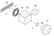
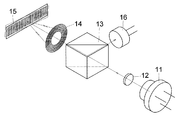
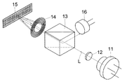
図1は第1の実施の形態のリニアエンコーダの構成図を示している。半導体レーザー光源11から射出する光束の光路上に、コリメータレンズ12、ビームスプリッタ13、円環状反射格子14、リニア回折格子スケール15が配列されており、ビームスプリッタ13の反射方向に受光素子16が配置されている。ここで、回折格子スケール15上の格子ピッチをP1とすると、円環状反射格子14はピッチP2=P1/2の関係に設定されている。
【0021】
このような構成により、半導体レーザー光源11から射出した光束Lは、コリメータレンズ12により略平行光束となり、ビームスプリッタ13、円環状反射格子14の中央部を透過して、回折格子スケール15に照射され、回折格子スケール15からの反射回折光L+、L−は、それぞれ円環状反射格子14上に照射される。円環状反射格子14は局所的に見ると格子ピッチP2のリニア回折格子として作用し、回折格子スケール15の同一位置に向けて照射されて再び回折し、それらの光束がそれぞれ重ね合わされてビームスプリッタ13まで戻される。
【0022】
この光束はそれぞれビームスプリッタ13によって半導体レーザー光源11と異なる方向に取り出され、干渉光束として受光素子16において検出される。なお、±1次回折光を使用した場合には、干渉の明暗周期は回折格子スケール15の1ピッチ分の移動に対して4周期である。
【0023】
図2は半導体レーザー光源11の発振波長が温度環境の変化等の要因により変化して、回折角が変った場合の光路ずれの説明図である。回折格子スケール15による回折光の回折角が変っても、円環状反射格子14により元の回折角で回折されるので、回折格子スケール15による再回折位置及び射出光束の状態は不変であり、干渉状態は安定しており、格子スケール15を放射状格子に変えても問題はない。
【0024】
図3は回折格子スケール15の位置をずらした場合の光路ずれの説明図である。検出ヘッドと回折格子スケール15のギャップが小さくなっても、円環状反射格子14により回折されるので、回折格子スケール15による再回折位置及び射出光束の状態は不変であり、干渉状態は安定している。これは格子を放射状格子に変えても問題がない。
【0025】
図4は回折格子スケール15と検出ヘッド部の設置角度をアジマス方向にずらした場合の光路ずれの説明図である。アジマス誤差が多少加わっても円環状反射格子14の作用により元の光路に回折されるので、回折格子スケール15で再回折位置及び射出光束の状態は不変であり、干渉状態は安定している。
【0026】
図5は回折格子スケール15と検出ヘッド部の設置角度に格子線を軸にしてチルト誤差を与えた場合の光路ずれの説明図である。チルト誤差が多少加わっても、回折格子スケール15に再回折位置及び射出光束の状態において、±1次回折光光束間には差は生じないので干渉状態は安定している。ただし、再回折位置自体はずれることになる。
【0027】
図6は回折格子スケール15と検出ヘッド部の設置角度に格子配列方位を軸にしてチルト誤差を与えた場合の光路ずれの説明図である。チルト誤差が多少加わっても、同様に±1次回折光光束間に差が生じないので干渉状態は安定しており、再回折位置自体はずれる。
【0028】
このように、反射光学素子として円環状反射格子14を採用することにより、小型性かつ高分解能で、取付誤差に寛容な性能を得ることができる。
【0029】
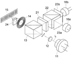
図7は第2の実施の形態の構成図を示し、位相差信号を発生させるように偏光素子を配置して、2相信号検出にしたものである。可干渉光源である半導体レーザー光源11の光路上に、コリメータレンズ12、非偏光ビームスプリッタ13、円環状反射格子14、偏光方位を互いに90度ずらした2個の偏光板20S、20P、回折格子スケール15が配列されている。非偏光ビームスプリッタ13の反射方向には、1/4波長板21、非偏光ビームスプリッタ22が配列されており、非偏光ビームスプリッタ22の反射方向に偏光板23a、受光素子16aが配置され、透過方向に偏光板23b、受光素子16bが配置されている。
【0030】
このような構成により、半導体レーザー光源11からの光束Lはコリメータレンズ12、非偏光ビームスプリッタ13を透過した後に、円環状反射格子14の中央の透過窓部を通って回折格子スケール15に略垂直に照射される。回折格子スケール15から反射された−1次回折光は回折角θで射出し、円環状反射格子14により元の光路に回折反射され、更に回折格子スケール15により−1次回折されて非偏光ビームスプリッタ13まで戻される。
【0031】
一方の反射された−1次回折光は回折角θで反対方向に射出し、円環状反射格子14により元の光路に回折反射され、更に回折格子スケール15により−1次回折されて、非偏光ビームスプリッタ13まで戻される。ここで、半導体レーザー光源11から回折格子スケール15に照射された光束は垂直及び水平方向の偏光成分を含んでおり、非偏光ビームスプリッタ13に伝播される±1次回折光は、明暗光束にはなっていないが、互いに偏光方位が90度ずれて波面が重なり合っている。
【0032】
この結果、非偏光ビームスプリッタ13により反射された両光束は1/4波長板21を透過し、2光束間の位相差に基づいて偏光方位が変化する直線偏光光束に変換され、後段の非偏光ビームスプリッタ22により2分割され、それぞれ偏光板23a、23bによって特定の偏光方位のみが抽出されて、それぞれ受光素子16a、16bによって明暗信号が受光される。これらそれぞれの明暗信号の位相(タイミング)は、偏光板23a、23bの偏光方位のずれで与えられる。即ち、偏光板23aと偏光板23bの偏光方位を互いに45度ずらすことによって、明暗信号の位相差は90度に設定される。
【0033】
図8は第3の実施の形態の構成図を示し、位相差信号を発生するように結晶光学素子を配置して、2相信号検出となっている。本実施の形態では、回折格子スケール15と円環状反射格子14の間の光路中の一方に、1/4波長板24が挿入されている。
【0034】
半導体レーザー光源11からの光束は、非偏光ビームスプリッタ13を透過した後に回折格子スケール15に略垂直に照射されている。回折格子スケール15から反射された+1次回折光は回折角θで射出し、1/4波長板24を通って円環状反射格子14に至り、円環状反射格子14で元の光路に回折反射され、再び回折格子スケール15により+1次回折して非偏光ビームスプリッタ13まで戻される。
【0035】
一方の反射された−1次回折光は回折角θにより反対方向に射出し、1/4波長板24を通って円環状反射格子14に至り、円環状反射格子14により元の光路に回折反射され、再び回折格子スケール15により−1次回折して非偏光ビームスプリッタ13まで戻される。ここで、半導体レーザー光源11から回折格子スケール15に照射された光束の偏光成分は1/4波長板24の光学軸に対して45度の関係になっており、1/4波長板24を往復透過した側のみ偏光方位が90度ずらされるために、非偏光ビームスプリッタ13に伝播される±1次回折光は明暗光束にはなっていないが、互いに偏光方位が90度ずれて波面が重なり合っている。
【0036】
その後は、第2の実施の形態と同様に、これらの両光束は1/4波長板21、非偏光ビームスプリッタ22を通り、それぞれ偏光板23a、23bを介して受光素子16a、16bによって明暗信号が受光される。
【0037】
図9は第4の実施の形態の構成図を示し、位相差信号を発生するように結晶光学素子が配置され、2相信号検出としている。本実施の形態では、回折格子スケール15と円環状反射格子14の間の光路中に1/8波長板25a、25bが互いに光学軸を90度ずらして挿入されている。
【0038】
半導体レーザー光源11からの光束Lは非偏光ビームスプリッタ13を透過した後に、回折格子スケール15に略垂直に照射される。回折格子スケール15から反射された+1次回折光は回折角θで射出し、1/8波長板25aを通って円環状反射格子14に至り、円環状反射格子14により元の光路に回折反射され、再び回折格子スケール15により+1次回折して非偏光ビームスプリッタ13まで戻される。
【0039】
一方の反射された−1次回折光は回折角θにより反対方向に射出し、1/8波長板25bを通って円環状反射格子14に至り、この円環状反射格子14により元の光路に回折反射され、再び回折格子スケール15により−1次回折されて、非偏光ビームスプリッタ13まで戻されている。ここで、半導体レーザー光源11から回折格子スケール15に照射された光束の偏光成分は、1/8波長板25a、25bの光学軸に対して45度の関係に設定されている。
【0040】
非偏光ビームスプリッタ13に伝播される±1次回折光は、互いに逆周りの円偏光光束となっているために、両者をベクトル合成すると、2光束間の位相差に基づいて偏光方位が変化する直線偏光光束に変換される。この光束は後段の非偏光ビームスプリッタ22により2分割され、それぞれを偏光板23a、23bにより特定の偏光方位のみが抽出され、それぞれの受光素子16a、16bにおいて明暗信号が受光される。
【0041】
図10は第5の実施の形態の構成図を示し、第4の実施の形態で円環状反射格子14の代りに円環状透過格子26が採用され、円環状透過格子26の直後にある反射面27により往復回折して、回折格子スケール15上に再照射するように構成されている。ここで、円環状透過格子26のピッチは回折格子スケール15のピッチと同じに設定されている。
【0042】
第4の実施の形態と同様に、半導体レーザー光源11からの光束は非偏光ビームスプリッタ13を透過して回折格子スケール15に照射され、その+1次反射回折光は回折角θで出射し、1/8波長板25aを通って円環状透過格子26により回折し、回折直後の反射面27により元の光路に戻され、再び円環状透過格子26により回折偏向し、回折格子スケール15により+1次回折されて非偏光ビームスプリッタ13まで戻される。
【0043】
一方の−1次反射回折光は回折角θにより反対方向に射出し、1/8波長板25bを通って円環状透過格子26により回折し、反射面27により元の光路に戻され、再び円環状透過格子26により回折偏向し、回折格子スケール15により−1次回折されて非偏光ビームスプリッタ13まで戻される。
【0044】
そして第4の実施の形態と同様に、±1次回折光は直線偏光光束に変換されて非偏光ビームスプリッタ22により2分割され、それぞれ偏光板23a、23bを介して受光素子16a、16bに明暗信号が受光される。
【0045】
なお、図10において位相差信号を得るためには、図7と同様に偏光板を挿入する方法や、図8に示すように位相差板を挿入する方法も適用可能である。また、これらの偏光状態変換素子は円環状透過格子26と反射面27の間に挿入してもよい。
【0046】
実際には、回折格子スケール15に照射する光束は有限の大きさを有するために、例えば格子ピッチが2.8μmの回折格子スケール15を使用して、この回折格子スケール15と円環状反射格子14との距離を10mmに設定した場合の光束追跡を行うと、図11に示すように円環状反射格子14に特有の波面ひずみが加わって長楕円状の波面となり、受光素子16において受光する際に損失が生ずることも想定される。
【0047】
更に、図12に示すように半径が9.2mm、1周の本数が20250本の放射状格子15’に、直径1mmの光束を照射した場合の光束追跡を行うと、円環状反射格子14特有の波面ひずみに更に放射状格子特有の波面ひずみが加わり、±1次回折光を合波する際に互いの波面が歪むことも想定される。
【0048】
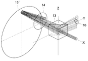
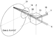
図13は第6の実施の形態のロータリエンコーダの構成図を示す。半導体レーザー光源11からの光束の光路上に、コリメータレンズ12、ビームスプリッタ13、レンズ30、円環状反射格子14、放射状回折格子スケール31が配列されており、ビームスプリッタ13の反射方向に受光素子16が配置されている。ここで、回折格子スケール31上の格子ピッチをP1とすると、円環状反射格子14はピッチP2=P1/2の関係に設定されている。
【0049】
このような構成により、半導体レーザー光源11から射出した光束Lは、コリメータレンズ12により略平行光束となり、ビームスプリッタ13、レンズ30、円環状反射格子14の中央部を透過して、放射状回折格子スケール31に集光照射され、放射状回折格子スケール31からの反射回折光L+、L−はそれぞれ円環状反射格子14上に略点状に照射される。
【0050】
なお、回折格子スケール31としてこのような放射状回折格子スケールを使用した場合には、放射状格子特有の収差によって完全には点状集光とはならない。また、リニア回折格子スケールを使用した場合でもレーザー光のビームウエストサイズ以下にはならないが、これらは微小量なために無視することができる。
【0051】
円環状反射格子14は局所的に見ると格子ピッチP2のリニア回折格子として作用し、回折格子スケール31の集光照明領域から射出する光束に対して、円環状反射格子14に略点状に入射した光束は反転して元の進路ヘ回折され、回折格子スケール31に向けて照射されて再び回折し、それらの光束がそれぞれ重ね合わされてビームスプリッタ13まで戻される。この光束はそれぞれビームスプリッタ13によって半導体レーザー光源11と異なる方向へ取り出され、干渉光束として受光素子16で検出される。なお、±1次回折光を使用した場合には、干渉の明暗周期は回折格子スケール31の2ピッチ分の移動につき4周期であり、図14、図15に示すように受光素子16上において略円形の光束が得られる。
【0052】
図16は半導体レーザー光源11の発振波長が温度環境の変化等の要因によってΔλ=10nmだけ変化して、回折角が変った場合の光路ずれの計算結果の説明図である。この場合には、回折格子スケール31による回折光の回折角が変って円環状反射格子14の照射位置が若干ずれているが、円環状反射格子14の作用により元の回折角で回折されるために、回折格子スケール31による再回折位置及び射出光束の状態は変らず、干渉状態は安定している。
【0053】
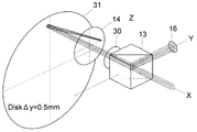
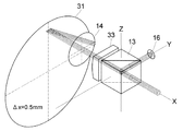
図17は回折格子スケール31の放射格子ディスクの位置をΔx=0.5mmだけずらした場合の光路ずれの説明図である。検出ヘッド部と回折格子スケール31のギャップが小さくなっても、円環状反射格子14で回折されることで、放射状回折格子スケール31による再回折位置及び射出光束の状態は変らず、干渉状態は安定している。
【0054】
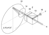
図18、図19は放射状回折格子スケール31に対して検出ヘッド部を接線方向にΔy=0.5mmだけずらした場合の光束の計算結果の説明図である。この場合は、回折格子スケール31の偏心が0.5mmの場合と等価であり、またリニア格子を使用した場合のスケール配置におけるアジマス誤差と等価である。照射位置がずれても円環状反射格子14の作用により元の光路に回折されるために、放射状回折格子スケール31による再回折位置及び射出光束の状態は変ることはない。
【0055】
また、図18、図19はそれぞれ+1次、−1次回折光の光路を示しており、受光素子16上では上下に多少ずれているが、互いに略平行光束であり干渉状態は安定している。なお、この0.5mmのずれはあくまで計算結果を分かり易くするための量であり、実際のエンコーダでのずれ量は更に少ない。
【0056】
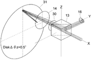
図20、図21は回折格子スケール31と検出ヘッド部の設置角度を、格子配列方位を軸にしてチルト誤差Δθz=0.5度だけ与えた場合の光路ずれの説明図である。±1次回折光の光路をそれぞれ読み取ると、チルト誤差が多少加わっても、回折格子スケール31による再回折位置及び射出光束の状態において、±1次回折光の光束間に差は生じないので干渉状態は安定している。
【0057】
なお、受光素子16上への入射光束が受光素子16の面からずれているが、0.5mmのずれは計算結果を分かり易くするための量であり、実際のエンコーダでのずれ量は更に少ない。
【0058】
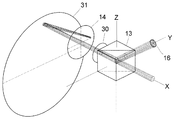
図22、図23は回折格子スケール31と検出ヘッド部の設置角度を、格子配列方位を軸にしてチルト誤差Δθy=0.5度だけ与えた場合の光路ずれの説明図である。この場合も、±1次回折光の光路をそれぞれ読み取ると、チルト誤差が多少加わっても回折格子スケール31による再回折位置及び射出光束の状態において、±1次回折光の光束間に差は生じないので干渉状態は安定しており、受光素子16の入射位置自体もほぼずれることはない。
【0059】
このように、反射型で円環状反射格子14とこの光学素子への点状の照射を組み合わせることによって、小型でかつ高分解能で、取付誤差に寛容な性能及び安定した干渉信号の検出を両立させることができる。
【0060】
図24は第7の実施の形態の斜視図を示し、位相差信号を発生するように偏光素子を配置して2相信号検出にしたものである。偏光素子として偏光板を使用し、またリニア回折レンズを使用したリニアエンコーダであり、偏光素子として1/4波長板を使用し、放射状回折レンズを使用したロータリエンコーダも可能である。
【0061】
可干渉光源である半導体レーザー光源11の光路上に、コリメータレンズ12、非偏光ビームスプリッタ13、レンズ30、円環状反射格子14、偏光方位を互いに90度ずらした2個の偏光板20S、20P、回折格子スケール15が配列されている。
【0062】
このような構成により、半導体レーザー光源11からの光束はコリメータレンズ12、非偏光ビームスプリッタ13を透過した後に、レンズ30、円環状反射格子14の中央部を介して回折格子スケール15に略垂直に照射される。先ず、回折格子スケール15から反射された+1次回折光は回折角θで射出し、円環状反射格子14により元の光路に回折反射され、更に回折格子スケール15により+1次回折されて非偏光ビームスプリッタ13まで戻される。
【0063】
一方の反射された−1次回折光は回折角θで反対方向に射出し、円環状反射格子14により元の光路に回折反射され、更に回折格子スケール15により−1次回折されて非偏光ビームスプリッタ13まで戻される。ここで、半導体レーザー光源11から回折格子スケール15に照射された光束は、垂直及び水平方向の偏光成分を含んでおり、非偏光ビームスプリッタ13に伝播される±1次回折光は、互いに偏光方位が90度ずれて波面が重なり合っているが、明暗光束にはなっていない。
【0064】
この結果、非偏光ビームスプリッタ13により反射された両光束は1/4波長板21を透過して、2光束間の位相差に基づいて偏光方位が変化する直線偏光光束に変換され、後段の非偏光ビームスプリッタ22により2分割され、それぞれが偏光板23a、23bによって特定の偏光方位のみが抽出されて明暗信号が得られる。これらそれぞれの明暗信号の位相(タイミング)は、偏光板23a、23bの偏光方位のずれで与えられる。即ち、偏光板23aと偏光板23bの偏光方位を互いに45度ずらすことによって、明暗信号の位相差は90度に設定される。
【0065】
図25は第8の実施の形態の光路図を示し、放射状回折格子スケール31を使用し、収束光束を照射する光学手段としてコリメータレンズ12を使用して直接収束光にしたものである。なお、図は非常に緩やかな収束光となっている。
【0066】
更に、図26は第9の実施の形態の構成図を示し、円環状反射格子14の中央部の透過窓部に回折レンズ32が一体的に形成されている。この回折レンズ32は中心付近の格子ピッチと周辺部の格子ピッチが連続的に変化してパターンニングされており、凸レンズの作用を有している。
【0067】
図27は第10の実施の形態におけるロータリエンコーダの光学配置図であり、図13の第6の実施の形態とほぼ同等の構成であるが、円環状反射格子14からの反射光が放射状回折格子スケール31に点状集光するようになっている。また、図28、図29はこの光学系に直径1mmの光束を入射させて±1次回折光の光線追跡を行った結果を図示したものである。
【0068】
半導体レーザー光源11から射出された光束は、ビームスプリッタ13を透過し、レンズ30を透過して収束光束になり、放射状回折格子スケール31に収束傾向より照明され、反射回折光L+、L−は、それぞれ円環状反射格子14上に照明される。ここで、回折格子スケール31上の格子ピッチをP1とすると、円環状反射格子14のピッチP2は、P2=P1/2の関係で設定されている。
【0069】
円環状反射格子14は局所的に見ると、格子ピッチP2のリニア回折格子として作用し、回折格子スケール31からの線状集光領域から射出してきた光束に対して円環状反射格子14に入射した光束はほぼ元の方位へ回折され、回折格子スケール31に向けて照明され、この際にレンズ30の作用によって点状に集光され、発散傾向の光束状態で再回折され、それぞれ光束を重ね合わせてビームスプリッタ13まで戻される。
【0070】
なお、復路における回折格子スケール31上での点状集光の程度として円環状反射格子14による線状集光収差があり、更に回折格子スケールとして放射状回折格子スケール31を使用した場合には、放射状回折格子スケール31特有の収差が加わり完全な点状集光にはならないが、それは微量で無視できる。
【0071】
本実施の形態では、放射状回折格子スケール31及び円環状反射格子14を部分としてリニア格子とした場合に、復路の回折格子スケール31上で点状集光するように設計されているが、実際は上述の収差によって点状集光の完全性は失われる。更に、収差を無視した場合の集光位置は、復路の回折格子スケール31上に完全に一致する必要はなく、円環状反射格子14〜回折格子スケール31の間であれば、干渉状態が安定する効果がある。なお、±1次回折光を使用した場合は、干渉の明暗周期は回折格子スケール31の1ピッチ分の移動につき4周期である。
【0072】
図28は放射状格子スケール31及び円環状反射格子14の光束照射部における格子配列方位のみの光束要素のみを計算し、図では円環状反射格子14〜受光素子16までの光束のみを選択して表示したものである。図28に示すように復路の放射状格子スケール31により略集光し、そこから発散光束として受光素子16まで進行している。また、図29は直径1mmの平行光束の各光束要素の光線追跡を光源11〜受光素子16まで行ったものであり、受光素子16上でほぼ楕円形の光束が得られている。
【0073】
図30はこの第10の実施の形態において、半導体レーザー光源11の発振波長が温度環境の変化等の要因により10nm変化し、回折角が変わった場合の光路ずれの計算結果である。回折角が変わって、円環状反射格子14の照明位置が若干ずれているが、円環状反射格子14で元の回折角により回折され、回折格子スケール31で再回折位置及び射出光束の状態は不変であり、干渉状態は勿論安定している。
【0074】
図31は第10の実施の形態において、放射状回折格子スケール31の位置を0.5mmずらした場合の光路ずれの説明図である。ギャップが大きくなっても円環状反射格子14により回折され、放射状格子スケール31で再回折位置及び射出光束の状態はほぼ不変であり、干渉状態は勿論安定している。
【0075】
図32は第10の実施の形態により放射状回折格子スケール31に対して検出ヘッド部を接線方向に0.5mmだけずらした場合の光線の計算結果である。放射状回折格子スケール31の偏芯が0.5mmの場合と等価であり、またリニア回折格子スケール15を使用した場合のスケール配置におけるアジマス誤差と等価である。照明位置がずれても円環状反射格子14の作用により元の光路に回折され、放射状回折格子スケール31で再回折位置及び射出光束の状態は不変である。
【0076】
図32、図33はそれぞれ±1次回折光の光路であるが、受光素子16上では上下に多少のずれが生じている。しかし、互いに略平行光束であり、干渉状態は安定している。なお、0.5mmのずれは、あくまで計算結果を分かり易くするための量であり、実際のエンコーダにおいては、更に少ない量である。
【0077】
図34、図35は第10の実施の形態において、放射状回折格子スケール31と検出ヘッド部の設置角度を格子線を軸によりチルト誤差Δθz=0.5度を与えた場合の光路ずれの説明図である。図34、図35の±1次回折光光路を読み取ると、チルト誤差が多少加わっても放射状回折格子スケール31に再回折位置及び射出光束の状態において、±1次回折光光束間に差が生じないので干渉状態は安定している。
【0078】
なお、第10の実施の形態において、受光素子16上では受光素子面から2つの次数の光束が互いに逆向きにZ軸方向にずれているが、このZ軸向き成分は略平行状態のため干渉状態の変化にはなり難い。更に、この計算における0.5mmのずれは、あくまで計算結果を分かり易くするための量であり、実際のエンコーダにおいては更に少ない量である。
【0079】
図36、図37は第10の実施の形態において、スケール格子と検出ヘッド部の設置角度を格子配列方位を軸によりチルト誤差Δθy=0.5度を与えた場合の光路ずれの説明図である。図36、図37の±1次回折光光路を読み取ると、チルト誤差が多少加わっても回折格子スケール31に再回折位置及び射出光束の状態において、±1次回折光光束間に差が生じないので干渉状態は安定している。受光素子16への入射位置自体もほぼずれることはない。
【0080】
このように、円環状反射格子14と復路放射状回折格子スケール31への点状集光照明を組み合わせることにより、小型性、高分解能、取付誤差に寛容な性能及び安定した干渉信号の検出が両立できることが分かる。
【0081】
図38は第11の実施の形態を示し、第10の実施の形態において位相差信号を発生させるように偏光素子を配置し、2相信号検出にしている。この図38の実施の形態では、回折格子スケール15と円環状反射格子14の間の光路中に偏光方位を互いに90度ずらした偏光板20S、20Pが挿入されており、リニア回折レンズを使用したリニアエンコーダの実施の形態であり、可干渉光源である半導体レーザー光源11からの光束を非偏光ビームスプリッタ13を透過させた後に回折格子スケール15に略垂直に照明している。
【0082】
先ず、反射+1次回折光は回折角θにより射出し、上方に配置した円環状反射格子14により元の光路に回折反射され、更に回折格子スケール15により+1次回折させられて、非偏光ビームスプリッタ13まで戻される。
【0083】
一方の反射された−1次回折光は、回折角θにより反対方向に射出し、上方に配置した円環状反射格子14により元の光路に回折反射させられ、更に回折格子スケール15により−1次回折させられて、非偏光ビームスプリッタ13まで戻されている。
【0084】
従って、非偏光ビームスプリッタ13に伝播される±1次回折光は、互いに偏光方位が90度ずれて波面が重なり合っており、明暗光束にはなっていない。
【0085】
非偏光ビームスプリッタ13で反射された両光束は、その後の1/4波長板21を透過し、2光束間の位相差に基づいて偏光方位が変化する直線偏光光束に変換され、後段の非偏光ビームスプリッタ22によって2分割され、それぞれを偏光板23a、23bを介して特定の偏光方位のみを抽出することで明暗信号が得られる。それぞれの明暗信号の位相(タイミング)は、偏光板23a、23bの偏光方位のずれで与えられ、偏光板23aと偏光板23bは互いに偏光方位を45度ずらすことで、明暗信号の位相差を90度に設定している。
【0086】
図39は第12の実施の形態を示し、収束光束を照明する光学手段として、レンズ30を採用せずに、図示しないコリメータレンズ12により直接収束光にしたものである。
【0087】
更に、図40は第13の実施の形態を示し、円環状反射格子14の中央部の透過窓部に、回折レンズ32が一体的に形成されている。回折レンズ32は中心付近の格子ピッチと周辺部の格子ピッチが連続的に変化してパターンニングしてあり、凸レンズの作用を有している。
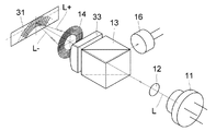
【0088】
図41は第14の実施の形態のロータリエンコーダの斜視図を示す。半導体レーザー光源11からの光束の光路上に、コリメータレンズ12、非偏光ビームスプリッタ13、シリンドリカルレンズ33、円環状反射格子14、放射状回折格子スケール31が配列されており、非偏光ビームスプリッタ13の反射方向に受光素子16が配置されている。ここで、放射状回折格子スケール31上の格子ピッチをP1とすると、円環状反射格子14はピッチP2=P1/2の関係に設定されている。
【0089】
このような構成により、半導体レーザー光源11から出射した光束Lは、コリメータレンズ12により略平行光束となり、非偏光ビームスプリッタ13、シリンドリカルレンズ33、円環状反射格子14の中央部の窓部を透過して、放射状回折格子スケール31に格子線配列方位又は接線方位に対して線状に照射され、放射状回折格子スケール31からの反射回折光L+、L−は、それぞれ円環状反射格子14上に長楕円状に照射される。ここで、回折格子スケール31に線状に照射されるのは、照射光束のシリンドリカルレンズ33による集光特性の結果であり、この照明光束と直交する軸方位にはシリンドリカルレンズ33のパワーは作用しないので、元の略平行特性のみを有する光束となっている。
【0090】
また、図42、図43は同一の光学系に直径1mmの光束を入射して、それぞれ±1次回折光の光束追跡を行った結果の説明図である。円環状反射格子14は局所的に見ると格子ピッチP2のリニア回折格子として作用し、放射状回折格子スケール31の線状集光領域から射出する光束に対して、円環状反射格子14のどの部分に入射した光束もほぼ元の方位へ回折し、回折格子スケール31の同一位置に向けて照射されて再び回折し、それらの光束がそれぞれ重ね合わされて非偏光ビームスプリッタ13まで戻される。これは円環状反射格子14の特有の効果である。
【0091】
この光束はそれぞれビームスプリッタ13によって半導体レーザー光源11と異なる方向へ取り出され、干渉光束として受光素子16において検出される。なお、±1次回折光を使用した場合には、干渉の明暗周期は放射状回折格子スケール31の1ピッチ分の移動に対して4周期であり、図42、図43に示すように受光素子16上において略円形の光束が得られる。
【0092】
図44は半導体レーザー光源11の発振波長が温度環境の変化等の要因によってΔλ=10nmだけ変化して、回折角が変った場合の光路ずれの計算結果の説明図である。放射状回折格子スケール31による回折光の回折角が変って、円環状反射格子14の照射位置が若干ずれているが、円環状反射格子14によって元の回折角で回折されるので、放射状回折格子スケール31による再回折位置及び射出光束の状態は変らず、干渉状態は安定している。
【0093】
図45は放射状回折格子スケール31の位置を、Δx=0.5mmだけずらした場合の光路ずれの説明図である。光束が照射されている位置の回折格子スケール31のギャップが小さくなっても円環状反射格子14で回折されて、回折格子スケール31による再回折位置及び射出光束の状態は変らず、干渉状態は安定している。
【0094】
図46、図47は放射状回折格子スケール31に対して検出ヘッド部を接線方向にΔy=0.5mmだけずらした場合の光束の計算結果の説明図である。放射状回折格子スケール31の偏心が0.5mmの場合と等価であり、またリニア回折格子スケールを使用した場合のスケール配置におけるアジマス誤差と等価である。照射位置がずれても円環状反射格子14の作用により元の光路に回折されるので、放射状回折格子による再回折位置及び射出光束の状態は変らない。
【0095】
これらの図46、図47はそれぞれ±1次回折光の光路を示しており、受光素子16上では上下に多少ずれているが、互いに略平行光束であり干渉状態は安定している。なお、この0.5mmのずれはあくまで計算結果を分かり易くするための量であり、実際のエンコーダではずれ量は更に少ない。
【0096】
図48、図49は放射状回折格子スケール31と検出ヘッド部の設置角度を、格子配列方位を軸にしてチルト誤差Δθz=0.5゜だけ与えた場合の光路ずれの説明図である。これらの図48、図49の±1次回折光の光路をそれぞれ読み取ると、チルト誤差が多少加わっても放射状回折格子スケール31による再回折位置及び射出光束の状態において、±1次回折光の光束間に差が生ずることはないので、干渉状態は安定している。なお、図48、図49では受光素子16上への入射光束が受光素子16の面からずれているが、0.5mmのずれは計算結果を分かり易くするための量であり、図46、図47の場合と同様に実際のエンコーダではずれ量は更に少ない。
【0097】
図50、図51は放射状回折格子スケール31と検出ヘッド部の設置角度を、格子配列方位を軸にしてチルト誤差Δθy=0.5゜だけ与えた場合の光路ずれの説明図である。図50、図51の±1次回折光の光路をそれぞれ読み取ると、チルト誤差が多少加わっても放射状回折格子スケール31による再回折位置及び射出光束の状態において、±1次回折光の光束間に差が生ずることはないので、干渉状態は安定しており、受光素子16の入射位置自体も殆ど変化することはない。
【0098】
このように、反射型で円環状反射格子14と線状照射を組み合わせることによって、小型性かつ高分解能で、取付誤差に寛容な性能及び安定した干渉信号の検出とを両立させることができる。
【0099】
図52は第15の実施の形態のエンコーダの斜視図を示し、偏光素子を有する位相差信号発生光学系を追加して2相の信号を検出している。なお、リニア型での回折格子スケール15を放射状回折格子スケール31に変えることによって、ロータリエンコーダとすることも可能である。
【0100】
可干渉光源である半導体レーザー光源11の光路上に、コリメータレンズ12、非偏光ビームスプリッタ13、シリンドリカルレンズ33、円環状反射格子14、偏光方位を互いに90度ずらした2個の偏光板20S、20P、回折格子スケール15が配列されている。非偏光ビームスプリッタ13の反射方向には1/4波長板21、非偏光ビームスプリッタ22が配列され、非偏光ビームスプリッタ22の反射方向に偏光板23a、受光素子16aが配置され、透過方向に偏光板23b、受光素子16bが配置されている。
【0101】
このような構成により、半導体レーザー光源11からの光束はコリメータレンズ12、非偏光ビームスプリッタ13を透過した後に、シリンドリカルレンズ33、円環状反射格子14の中央の透過窓部を通って回折格子スケール15に略垂直に方向から照射される。先ず、回折格子スケール15から反射された+1次回折光は回折角θで射出し、上方に配置された円環状反射格子14により元の光路に回折反射され、更に回折格子スケール15によって+1次回折されて非偏光ビームスプリッタ13まで戻される。
【0102】
一方の反射された−1次回折光は回折角θで反対方向に射出し、上方に配置された円環状反射格子14により元の光路に回折反射され、更に回折格子スケール15により−1次回折されて非偏光ビームスプリッタ13まで戻される。
【0103】
ここで、半導体レーザー光源11から回折格子スケール15に照射された光束は垂直及び水平方向の偏光成分を含んでおり、従って非偏光ビームスプリッタ13に伝播される±1次回折光は、互いに偏光方位が90度ずれて波面が重なり合っているが、明暗光束にはなっていない。
【0104】
この結果、非偏光ビームスプリッタ13により反射された両光束は1/4波長板21を透過し、2光束間の位相差に基づいて偏光方位が変化する直線偏光光束に変換され、後段の非偏光ビームスプリッタ22により2分割され、それぞれが偏光板23a、23bによって特定の偏光方位のみが抽出されて明暗信号が得られる。これらそれぞれの明暗信号の位相(タイミング)は、偏光板23a、23bの偏光方位のずれで与えられる。即ち、偏光板23aと偏光板23bの偏光方位を互いに45度ずらすことによって、明暗信号の位相差は90度に設定される。
【0105】
図53は第16の実施の形態を示し、線状に集光して光束を照射する光学手段としてリニア回折レンズ(リニア型フレネルゾーンプレート)34が使用されている。即ち、リニア回折レンズ34では円環状反射格子14の中央の透過窓部に回折レンズ35が一体的に形成されている。このリニア回折レンズ34は中心付近の格子ピッチと周辺部の格子ピッチが連続的に変化するようにパターンニングされており、位相差信号を発生するために結晶光学素子を配置して2相の信号を検出し、シリンドリカルレンズ33の作用を有している。
【0106】
図54は第17の実施の形態を示し、円環状反射格子14の代りに円環状透過格子36が採用され、円環状透過格子36の直後に設けられた反射面37により往復回折して、回折格子スケール15上に再照射する構成とされている。なお、円環状透過格子36のピッチは回折格子スケール15のピッチと同じに設定されている。
【0107】
可干渉光源である半導体レーザー光源11の光路上に、コリメータレンズ12、非偏光ビームスプリッタ13、シリンドリカルレンズ33、直後に反射面37を有する環状透過格子36、偏光方位を互いに90度ずらした位置にある2個の偏光板20S、20P、回折格子スケール15が配列されている。
【0108】
このような構成により、半導体レーザー光源11からの光束はコリメータレンズ12、非偏光ビームスプリッタ13、円環状透過格子36の中央窓部を透過した後に、シリンドリカルレンズ33を介して回折格子スケール15に略垂直方向から照射されている。先ず、回折格子スケール15から反射された+1次回折光は回折角θで射出され、上方に配置した円環状透過格子36により回折した直後の反射面37において元の光路に戻され、再び円環状透過格子36により回折偏向し、更に回折格子スケール15において+1次回折して非偏光ビームスプリッタ13まで戻される。
【0109】
一方の反射された−1次回折光は回折角θで反対方向に射出され、上方に配置された円環状透過格子36により回折した直後に反射面37において元の光路に戻され、再び円環状透過格子36により回折偏向し、更に回折格子スケール15により−1次回折して非偏光ビームスプリッタ13まで戻される。
【0110】
半導体レーザー光源11から回折格子スケール15に照射された光束の偏光成分は、偏光板20S、20Pの光学軸に対して45゜の関係に設定されているために、非偏光ビームスプリッタ13に伝播される±1次回折光は、互いに直交した偏光面の直線偏光光束となっているおり、1/4波長板21を透過して両者をベクトル合成すると、2光束間の位相差に基づいて偏光方位が変化する直線偏光光束に変換される。従って、非偏光ビームスプリッタ22において2分割された光束のそれぞれを、偏光板23a、23bにより特定の偏光方位のみを抽出することによって明暗信号が得られる。これらの明暗信号それぞれの位相(タイミング)は、偏光板23a、23bの偏光方位のずれで与えられるので、偏光板23aと偏光板23bを互いに偏光方位を45度ずらすことによって、明暗信号の位相差は90゜に設定される。
【0111】
図52〜図54において、位相差信号を得るために偏光板20S、20P、23a、23bの代りに位相差板を挿入する方法も用いることができる。更に、図50においてこれらの偏光状態変換素子を円環状透過格子36と反射面37の間に挿入してもよい。
【0112】
また、上述の実施の形態においては、次の項目に関して部分変更の置き換えが可能である。
【0113】
(a)回折格子スケール15及び放射状回折格子スケール31又は円環状反射格子14において、±1次回折光以外の回折次数の回折光を使用する。
【0114】
(b)偏光板20S、20P、23a、23bをこれと同等な機能を有する他の素子である偏光膜付きプリズムや微細格子パターンとする。
【0115】
(c)位相差板即ち1/4波長板21や1/8波長板を水晶等の結晶光学素子と同等な機能を有する微細構造パターンや他の異方性材料とする。
【0116】
(d)位相差信号を2相以上として位相差を90度以外に設定し、更に偏光素子や位相差板の配置を一部変更して同等な効果を得る。
【0117】
(e)回折格子スケール15に投光する光束と再回折された光束を、受光素子16に導くために非偏光ビームスプリッタ13、22を使用しているが、回折格子等の他のビーム分割合成手段を使用したり、往路と復路の光路を空間的にずらすことにより分離したり、更に一方の光束のみを選択反射して受光素子16の側に導いてもよい。
【0118】
(f)コリメータレンズ12、非偏光ビームスプリッタ13、レンズ30、円環状反射格子14の配列順序を変えたりして、他の光学配置を採用して回折格子スケール15上に線状に集光する関係を満足させる。
【0119】
(g)シリンドリカルレンズ33を同等な機能を有する光学素子に変更する。
【0120】
(h)シリンドリカルレンズ33と円環状反射格子14又は円環状透過格子36を一体化する。例えば、シリンドリカルレンズ33の平面側に円環状反射格子14を形成する。
【0121】
(i)シリンドリカルレンズ33の機能とコリメータレンズ12の機能をトーリックレンズやホログラムレンズにより代替する。
【0122】
以上の各実施の形態では、円環状反射格子としては例えばガラスエッチング等により加工されたガラス板の裏面に反射膜を蒸着した素子が利用できるので、耐環境性が良好である。
【0123】
【発明の効果】
以上説明したように本発明による光学式エンコーダ及び回折格子の変位測定方法は、回折格子や円環状回折格子への照射状態を最適化することによって、次に列挙する効果が得られる。
【0124】
(1)例えば、平面状の光学素子を使用できるために、キャッツアイのように配置空間が複雑にならずかつ小型化に向いている。
【0125】
(2)光源の波長変動に対して補正が働くので干渉信号が安定する。
【0126】
(3)アライメント誤差に対して補正が働くために、回折格子スケールと検出ヘッドを分離したエンコーダでも取り付けが比較的容易になる。
【0127】
(4)再帰光学素子が小型でかつ部品点数が少ないために、光束照射手段に更に偏向手段を付加することよって、回折格子スケールへの照射方法や向きに自由度が高くなり、広範な適用姿勢が得られる。
【0128】
(5)回折光同士の干渉波面が相互に一致し易くなり、フラットな明暗パターンが得られ、SN比の良好な安定したエンコーダ信号を得ることができる。
【0129】
(6)再帰光学素子が小型でかつ部品点数が少ないために、光束照射手段に更に偏向手段を付加することによって、回折格子スケールへの照射方法や向きに自由度が高くなり、広範な適用姿勢が得られる。
【0130】
(7)再回折した回折光がそれ程広がらずに、受光素子に導かれるようにできるために、損失が少なくSN比の良好な検出を行うことができる。
【図面の簡単な説明】
【図1】第1の実施の形態のエンコーダの構成図である。
【図2】光源波長変化の影響の説明図である。
【図3】スケールと検出ヘッドのギャップ変化の説明図である。
【図4】スケールと検出ヘッドのアジマス角度変化の影響の説明図である。
【図5】スケールと検出ヘッドのチルト角度変化の影響の説明図である。
【図6】スケールと検出ヘッドのチルト角度変化の影響の説明図である。
【図7】第2の実施の形態のエンコーダの構成図である。
【図8】第3の実施の形態のエンコーダの構成図である。
【図9】第4の実施の形態のエンコーダの構成図である。
【図10】第5の実施の形態のエンコーダの構成図である。
【図11】光束追跡結果の説明図である。
【図12】光束追跡結果の説明図である。
【図13】第6の実施の形態のエンコーダの構成図である。
【図14】光束追跡結果の説明図である。
【図15】光束追跡結果の説明図である。
【図16】光束波長変化の影響の説明図である。
【図17】スケールと検出ヘッドのギャップ変化の影響の説明図である。
【図18】スケールと検出ヘッドのギャップ変化の影響の説明図である。
【図19】スケールと検出ヘッドのギャップ変化の影響の説明図である。
【図20】スケールと検出ヘッドのチルト角度変化の影響の説明図である。
【図21】スケールと検出ヘッドのチルト角度変化の影響の説明図である。
【図22】スケールと検出ヘッドのチルト角度変化の影響の説明図である。
【図23】スケールと検出ヘッドのチルト角度変化の影響の説明図である。
【図24】第7の実施の形態のエンコーダの構成図である。
【図25】第8の実施の形態のエンコーダの構成図である。
【図26】第9の実施の形態のエンコーダの構成図である。
【図27】本発明の第10の実施の形態の光学構成図である。
【図28】光束追跡結果の説明図である。
【図29】光束追跡結果の説明図である。
【図30】光源波長変化の影響の説明図である。
【図31】スケールと検出ヘッドのギャップの変化の影響の説明図である。
【図32】スケールと検出ヘッドのギャップの変化の影響の説明図である。
【図33】スケールと検出ヘッドのギャップの変化の影響の説明図である。
【図34】スケールと検出ヘッドのチルト角度変化の影響の説明図である。
【図35】スケールと検出ヘッドのチルト角度変化の影響の説明図である。
【図36】スケールと検出ヘッドのチルト角度変化の影響の説明図である。
【図37】スケールと検出ヘッドのチルト角度変化の影響の説明図である。
【図38】第11の実施の形態の構成図である。
【図39】第12の実施の形態の光路追跡結果の説明図である。
【図40】第13の実施の形態の光路追跡結果の説明図である。
【図41】第14の実施の形態の説明図である。
【図42】光束追跡結果の説明図である。
【図43】光束追跡結果の説明図である。
【図44】光束波長変化の影響の説明図である。
【図45】スケールと検出ヘッドのギャップ変化の影響の説明図である。
【図46】スケールと検出ヘッドのギャップ変化の影響の説明図である。
【図47】スケールと検出ヘッドのギャップ変化の影響の説明図である。
【図48】スケールと検出ヘッドのチルト角度変化の影響の説明図である。
【図49】スケールと検出ヘッドのチルト角度変化の影響の説明図である。
【図50】スケールと検出ヘッドのチルト角度変化の影響の説明図である。
【図51】スケールと検出ヘッドのチルト角度変化の影響の説明図である。
【図52】第15の実施の形態の構成図である。
【図53】第16の実施の形態の構成図である。
【図54】第17の実施の形態の構成図である。
【図55】従来例のエンコーダの構成図である。
【符号の説明】
11 半導体レーザー光源
12 コリメータレンズ
13、22 ビームスプリッタ
14 円環状反射格子
15 リニア回折格子スケール
16 受光素子
20、23 偏光板
21、24 1/4波長板
25 1/8波長板
26、36 円環状透過格子
27、37 反射面
31 放射状回折格子スケール
32 回折レンズ
33 シリンドリカルレンズ
34 リニア回折レンズ[0001]
BACKGROUND OF THE INVENTION
The present invention has a reflection mechanism using an annular diffraction grating for detecting position and angle information in, for example, industrial measuring machines. Optical encoder and diffraction grating displacement measuring method It is about.
[0002]
[Prior art]
FIG. 55 shows a configuration diagram of a conventional linear encoder, in which a light beam from a semiconductor
[0003]
The S-polarized light beam reflected by one
[0004]
Here, since the quarter-
[0005]
Since the phase (timing) of each of the light and dark signals is given by the deviation of the polarization direction of the polarizing
[0006]
The reflective
[0007]
For this reason, by using the reflection
[0008]
[Problems to be solved by the invention]
However, in the above-described conventional example, the reflective
[0009]
Further, in the case of a rotary encoder, a radial diffraction grating is used as the
[0010]
As a result, the phenomenon that the orientation of the re-diffracted light is deviated occurs, and this influence becomes larger as the grating pitch is finer on the micron order and the diameter (disk diameter) of the radiation grating scale is smaller. In the case where the
[0011]
In addition, this type of grating interferometric encoder employs a micron-order fine scale, and by extracting and interfering with two light beams diffracted by this scale, an encoder with much higher resolution than a geometric optical encoder can be obtained. ing.
[0012]
This encoder employs a configuration that generates an interference pattern by synthesizing the wavefronts of two diffracted lights. However, since it is an interference optical system, the processing and placement accuracy of each optical element is very strict at present. . In particular, in the case of a built-in encoder in which the scale unit and the detection head unit are separated, the user must mount the scale and the detection head on a motor, a stage, etc., so the difficulty of the work becomes a problem. ing.
[0013]
An object of the present invention is to solve the above-described problems and to obtain a good S / N ratio and perform stable light beam detection using an optical path deviation correcting optical system instead of a cat's eye. Optical encoder and diffraction grating displacement measuring method Is to provide.
[0014]
[Means for Solving the Problems]
In order to achieve the above object, an optical encoder according to the present invention includes a light source, an illumination optical system for causing light from the light source to enter the diffraction grating, and two diffracted lights generated by the diffraction grating. An annular grating that re-illuminates the diffraction grating with the two diffracted lights of (2) and an interference light that is generated when the two diffracted lights re-irradiated on the diffraction grating are re-diffracted by the diffraction grating and are superimposed on each other. An incident light beam deflecting unit; and a light receiving unit that receives the interference light emitted from the beam deflecting unit. Until the diffraction grating is re-irradiated In shape Focused It is characterized by that.
[0015]
The method for measuring the displacement of a diffraction grating according to the present invention is a method for measuring the displacement of a diffraction grating, the step of causing light from a light source to enter the diffraction grating, and two diffracted lights generated by the diffraction grating. Are incident on the annular grating, the step of re-irradiating the diffraction grating with the two diffracted lights incident on the annular grating, and the two diffracted lights re-irradiated on the diffraction grating by the diffraction grating Receiving the interference light that is re-diffracted and superposed on them, and the two diffracted lights generated by the diffraction grating are Until the diffraction grating is re-irradiated In shape Focused It is characterized by that.
[0020]
DETAILED DESCRIPTION OF THE INVENTION
The present invention will be described in detail based on the embodiment shown in FIGS.
FIG. 1 shows a configuration diagram of a linear encoder according to the first embodiment. A
[0021]
With such a configuration, the light beam L emitted from the semiconductor
[0022]
Each of the light beams is extracted in a direction different from that of the semiconductor
[0023]
FIG. 2 is an explanatory diagram of the optical path deviation when the oscillation angle of the semiconductor
[0024]
FIG. 3 is an explanatory diagram of the optical path deviation when the position of the
[0025]
FIG. 4 is an explanatory diagram of the optical path deviation when the installation angle of the
[0026]
FIG. 5 is an explanatory diagram of an optical path deviation when a tilt error is given to the installation angle of the
[0027]
FIG. 6 is an explanatory diagram of an optical path deviation when a tilt error is given to the installation angle of the
[0028]
As described above, by adopting the annular reflecting grating 14 as the reflecting optical element, it is possible to obtain a performance that is small in size and high in resolution and that is tolerant of mounting errors.
[0029]
FIG. 7 shows a configuration diagram of the second embodiment, in which a polarizing element is arranged to generate a phase difference signal and two-phase signal detection is performed. On the optical path of the semiconductor
[0030]
With such a configuration, the light beam L from the semiconductor
[0031]
One reflected -1st order diffracted light exits in the opposite direction at a diffraction angle θ, is diffracted and reflected back to the original optical path by the annular reflecting grating 14, and further -1st order diffracted by the
[0032]
As a result, both light beams reflected by the
[0033]
FIG. 8 shows a configuration diagram of the third embodiment, in which a crystal optical element is arranged so as to generate a phase difference signal, and two-phase signal detection is performed. In the present embodiment, a ¼
[0034]
The light beam from the semiconductor
[0035]
One reflected first-order diffracted light is emitted in the opposite direction at the diffraction angle θ, passes through the quarter-
[0036]
After that, as in the second embodiment, these two light beams pass through the quarter-
[0037]
FIG. 9 shows a configuration diagram of the fourth embodiment, in which crystal optical elements are arranged so as to generate a phase difference signal, and two-phase signal detection is performed. In the present embodiment, 1/8
[0038]
The light beam L from the semiconductor
[0039]
One reflected first-order diffracted light is emitted in the opposite direction by the diffraction angle θ, passes through the 8
[0040]
Since the ± first-order diffracted light propagated to the
[0041]
FIG. 10 shows a configuration diagram of the fifth embodiment. In the fourth embodiment, an annular transmission grating 26 is employed instead of the annular reflection grating 14, and a reflection surface immediately after the annular transmission grating 26 is shown. The
[0042]
Similar to the fourth embodiment, the light beam from the semiconductor
[0043]
On the other hand, the minus first-order reflected diffracted light is emitted in the opposite direction by the diffraction angle θ, is diffracted by the annular transmission grating 26 through the 8
[0044]
Similarly to the fourth embodiment, the ± first-order diffracted light is converted into a linearly polarized light beam and divided into two by a
[0045]
In addition, in order to obtain a phase difference signal in FIG. 10, the method of inserting a polarizing plate similarly to FIG. 7 and the method of inserting a phase difference plate as shown in FIG. 8 are applicable. These polarization state conversion elements may be inserted between the annular transmission grating 26 and the
[0046]
Actually, since the light beam applied to the
[0047]
Furthermore, as shown in FIG. 12, when the light beam tracking is performed when the radial grating 15 ′ having a radius of 9.2 mm and the number of rounds of 20250 is irradiated with a light beam having a diameter of 1 mm, a characteristic peculiar to the annular reflection grating 14 is obtained. It is also assumed that wavefront distortion peculiar to the radial grating is added to the wavefront distortion, and the wavefronts of each other are distorted when the first-order diffracted light is combined.
[0048]
FIG. 13 is a configuration diagram of a rotary encoder according to the sixth embodiment. A
[0049]
With such a configuration, the light beam L emitted from the semiconductor
[0050]
Note that when such a radial diffraction grating scale is used as the
[0051]
The annular reflection grating 14 acts as a linear diffraction grating having a grating pitch P2 when viewed locally, and enters the annular reflection grating 14 in a substantially dotted manner with respect to the light beam emitted from the focused illumination region of the
[0052]
FIG. 16 is an explanatory diagram of the calculation result of the optical path deviation when the oscillation wavelength of the semiconductor
[0053]
FIG. 17 is an explanatory diagram of the optical path deviation when the position of the radiation grating disk of the
[0054]
18 and 19 are explanatory diagrams of calculation results of the light flux when the detection head portion is shifted in the tangential direction by Δy = 0.5 mm with respect to the radial
[0055]
FIGS. 18 and 19 show the optical paths of the + 1st order and −1st order diffracted lights, respectively, which are slightly shifted up and down on the
[0056]
FIG. 20 and FIG. 21 are explanatory diagrams of the optical path deviation when the installation angle of the
[0057]
Although the incident light beam on the
[0058]
22 and 23 are explanatory diagrams of the optical path deviation when the installation angle of the
[0059]
In this way, by combining the reflection type annular reflection grating 14 and the point-like irradiation to the optical element, it is possible to achieve both small size, high resolution, tolerance for mounting errors, and stable detection of interference signals. be able to.
[0060]
FIG. 24 is a perspective view of the seventh embodiment, in which a polarizing element is arranged so as to generate a phase difference signal and two-phase signal detection is performed. A linear encoder using a polarizing plate as a polarizing element and a linear diffractive lens, and a rotary encoder using a quarter-wave plate as a polarizing element and a radial diffractive lens are also possible.
[0061]
On the optical path of the semiconductor
[0062]
With such a configuration, the light beam from the semiconductor
[0063]
One reflected -1st order diffracted light is emitted in the opposite direction at a diffraction angle θ, is diffracted and reflected back to the original optical path by the annular reflecting grating 14, and further -1st order diffracted by the
[0064]
As a result, both light beams reflected by the
[0065]
FIG. 25 shows an optical path diagram of the eighth embodiment, in which a radial
[0066]
Further, FIG. 26 shows a configuration diagram of the ninth embodiment, in which a
[0067]
FIG. 27 is an optical layout diagram of the rotary encoder in the tenth embodiment, and the configuration is almost the same as that of the sixth embodiment in FIG. 13, but the reflected light from the annular reflecting grating 14 is a radial diffraction grating. The
[0068]
Semiconductor
[0069]
When viewed locally, the annular reflection grating 14 acts as a linear diffraction grating with a
[0070]
In addition, there is a linear condensing aberration due to the annular reflecting grating 14 as the degree of point condensing on the
[0071]
In the present embodiment, when the radial
[0072]
In FIG. 28, only the light beam elements having only the lattice arrangement direction in the light beam irradiation part of the radial grating
[0073]
FIG. 30 shows a calculation result of the optical path deviation when the oscillation wavelength of the semiconductor
[0074]
FIG. 31 is an explanatory diagram of an optical path shift when the position of the radial
[0075]
FIG. 32 shows the calculation result of the light beam when the detection head unit is shifted by 0.5 mm in the tangential direction with respect to the radial
[0076]
FIGS. 32 and 33 are optical paths of ± first-order diffracted light, respectively, but a slight shift occurs vertically on the
[0077]
FIGS. 34 and 35 are diagrams for explaining the optical path deviation when the tilt angle Δθz = 0.5 degrees is given with respect to the installation angle of the radial
[0078]
In the tenth embodiment, on the
[0079]
FIG. 36 and FIG. 37 are explanatory diagrams of the optical path deviation when the tilt angle Δθy = 0.5 degrees is given with respect to the installation angle of the scale grating and the detection head unit as the axis of the grating arrangement direction in the tenth embodiment. . When the ± 1st order diffracted light paths in FIGS. 36 and 37 are read, even if a tilt error is slightly added, there is no difference between the ± 1st order diffracted light beams in the
[0080]
In this way, by combining the annular reflecting grating 14 and the point-shaped condensed illumination on the return radial
[0081]
FIG. 38 shows an eleventh embodiment. In the tenth embodiment, a polarizing element is arranged so as to generate a phase difference signal, and two-phase signal detection is performed. In the embodiment of FIG. lattice In the optical path between the
[0082]
First, the reflected + 1st order diffracted light is emitted at a diffraction angle θ, diffracted and reflected to the original optical path by the annular reflecting grating 14 disposed above, and further + 1st order diffracted by the
[0083]
One of the reflected -1st order diffracted lights is emitted in the opposite direction by the diffraction angle θ, is diffracted and reflected to the original optical path by the annular reflecting grating 14 disposed above, and is further -1st order diffracted by the
[0084]
Accordingly, the ± first-order diffracted lights propagated to the
[0085]
The two light beams reflected by the
[0086]
FIG. 39 shows a twelfth embodiment and does not illustrate the
[0087]
FIG. 40 shows a thirteenth embodiment, in which a
[0088]
FIG. 41 is a perspective view of a rotary encoder according to the fourteenth embodiment. A
[0089]
With such a configuration, the light beam L emitted from the semiconductor
[0090]
FIG. 42 and FIG. 43 are explanatory diagrams of the results of tracking a ± 1st order diffracted light beam by entering a 1 mm diameter light beam into the same optical system. When viewed locally, the annular reflection grating 14 acts as a linear diffraction grating with a
[0091]
Each of these light beams is extracted in a direction different from that of the semiconductor
[0092]
FIG. 44 is an explanatory diagram of the calculation result of the optical path deviation when the oscillation wavelength of the semiconductor
[0093]
FIG. 45 is an explanatory diagram of the optical path deviation when the position of the radial
[0094]
46 and 47 are explanatory diagrams of calculation results of the light flux when the detection head unit is shifted in the tangential direction by Δy = 0.5 mm with respect to the radial
[0095]
46 and 47 show the optical paths of the ± first-order diffracted lights, which are slightly shifted up and down on the
[0096]
FIG. 48 and FIG. 49 are explanatory diagrams of the optical path deviation when the installation angle of the radial
[0097]
FIG. 50 and FIG. 51 are explanatory diagrams of the optical path deviation when the installation angle of the radial
[0098]
In this manner, by combining the reflection type annular reflection grating 14 and linear irradiation, it is possible to achieve both compactness and high resolution, tolerance for mounting errors, and stable detection of interference signals.
[0099]
FIG. 52 is a perspective view of an encoder according to the fifteenth embodiment, in which a phase difference signal generating optical system having a polarizing element is added to detect a two-phase signal. Note that a rotary encoder can be obtained by changing the linear
[0100]
On the optical path of the semiconductor
[0101]
With such a configuration, the light flux from the semiconductor
[0102]
One of the reflected -1st order diffracted lights is emitted in the opposite direction at the diffraction angle θ, is diffracted and reflected to the original optical path by the annular reflecting grating 14 disposed above, and further -1st order diffracted by the
[0103]
Here, the light beam emitted from the semiconductor
[0104]
As a result, both light beams reflected by the
[0105]
FIG. 53 shows a sixteenth embodiment, in which a linear diffractive lens (linear Fresnel zone plate) 34 is used as optical means for condensing linearly and irradiating a light beam. That is, in the
[0106]
FIG. 54 shows a seventeenth embodiment, in which an annular transmission grating 36 is employed instead of the annular reflection grating 14, and diffraction is performed by reciprocal diffraction by a
[0107]
On the optical path of the semiconductor
[0108]
With such a configuration, the light flux from the semiconductor
[0109]
One reflected first-order diffracted light is emitted in the opposite direction at a diffraction angle θ, and immediately after being diffracted by the annular transmission grating 36 disposed above, is returned to the original optical path at the
[0110]
The polarization component of the light beam applied to the
[0111]
52 to 54, a method of inserting a phase difference plate in place of the
[0112]
Further, in the above-described embodiment, partial changes can be replaced with respect to the following items.
[0113]
(A) In the
[0114]
(B) The
[0115]
(C) A phase difference plate, that is, a
[0116]
(D) The phase difference signal is set to two or more phases, the phase difference is set to other than 90 degrees, and the arrangement of the polarizing element and the phase difference plate is partially changed to obtain an equivalent effect.
[0117]
(E) The
[0118]
(F) The
[0119]
(G) The
[0120]
(H) The
[0121]
(I) The function of the
[0122]
In each of the above embodiments, as the annular reflection grating, for example, an element in which a reflective film is deposited on the back surface of a glass plate processed by glass etching or the like can be used.
[0123]
【The invention's effect】
As explained above, according to the present invention. Optical encoder and diffraction grating displacement measuring method The following effects can be obtained by optimizing the irradiation state of the diffraction grating and the annular diffraction grating.
[0124]
(1) For example, since a planar optical element can be used, the arrangement space is not complicated as in the case of a cat's eye and is suitable for miniaturization.
[0125]
(2) Since the correction works for the wavelength variation of the light source, the interference signal is stabilized.
[0126]
(3) Since the correction works for the alignment error, it is relatively easy to mount the encoder even if the diffraction grating scale and the detection head are separated.
[0127]
(4) Since the retroreflective optical element is small and has a small number of parts, adding a deflecting unit to the light beam irradiating unit increases the degree of freedom in the irradiation method and direction of the diffraction grating scale, and can be used in a wide range of applications. Is obtained.
[0128]
(5) The interference wavefronts of the diffracted light easily match each other, a flat light / dark pattern is obtained, and a stable encoder signal with a good SN ratio can be obtained.
[0129]
(6) Since the recursive optical element is small and has a small number of parts, a deflecting means is added to the light beam irradiating means. In Therefore, the degree of freedom in the irradiation method and direction of the diffraction grating scale is increased, and a wide range of application postures can be obtained.
[0130]
(7) Since the re-diffracted diffracted light can be guided to the light receiving element without spreading so much, detection with a low loss and good SN ratio can be performed.
[Brief description of the drawings]
FIG. 1 is a configuration diagram of an encoder according to a first embodiment.
FIG. 2 is an explanatory diagram of an influence of a light source wavelength change.
FIG. 3 is an explanatory diagram of a change in a gap between a scale and a detection head.
FIG. 4 is an explanatory diagram of the influence of a change in azimuth angle between a scale and a detection head.
FIG. 5 is an explanatory diagram of an influence of a tilt angle change of a scale and a detection head.
FIG. 6 is an explanatory diagram of an influence of a change in tilt angle of a scale and a detection head.
FIG. 7 is a configuration diagram of an encoder according to a second embodiment.
FIG. 8 is a configuration diagram of an encoder according to a third embodiment.
FIG. 9 is a configuration diagram of an encoder according to a fourth embodiment.
FIG. 10 is a configuration diagram of an encoder according to a fifth embodiment.
FIG. 11 is an explanatory diagram of a light beam tracking result.
FIG. 12 is an explanatory diagram of a light beam tracking result.
FIG. 13 is a configuration diagram of an encoder according to a sixth embodiment.
FIG. 14 is an explanatory diagram of a light beam tracking result.
FIG. 15 is an explanatory diagram of a light beam tracking result;
FIG. 16 is an explanatory diagram of the influence of a change in light beam wavelength.
FIG. 17 is an explanatory diagram of the influence of a change in the gap between the scale and the detection head.
FIG. 18 is an explanatory diagram of the influence of a change in the gap between the scale and the detection head.
FIG. 19 is an explanatory diagram of the influence of a change in the gap between the scale and the detection head.
FIG. 20 is an explanatory diagram of an influence of a tilt angle change of a scale and a detection head.
FIG. 21 is an explanatory diagram of an influence of a tilt angle change of a scale and a detection head.
FIG. 22 is an explanatory diagram of an influence of a tilt angle change of a scale and a detection head.
FIG. 23 is an explanatory diagram of the influence of a change in the tilt angle of the scale and the detection head.
FIG. 24 is a configuration diagram of an encoder according to a seventh embodiment.
FIG. 25 is a configuration diagram of an encoder according to an eighth embodiment.
FIG. 26 is a configuration diagram of an encoder according to a ninth embodiment.
FIG. 27 is an optical configuration diagram of a tenth embodiment of the present invention.
FIG. 28 is an explanatory diagram of a light beam tracking result.
FIG. 29 is an explanatory diagram of a light beam tracking result.
FIG. 30 is an explanatory diagram of the influence of a light source wavelength change.
FIG. 31 is an explanatory diagram of the influence of a change in the gap between the scale and the detection head.
FIG. 32 is an explanatory diagram of the influence of a change in the gap between the scale and the detection head.
FIG. 33 is an explanatory diagram of the influence of a change in the gap between the scale and the detection head.
FIG. 34 is an explanatory diagram of an influence of a tilt angle change of a scale and a detection head.
FIG. 35 is an explanatory diagram of the influence of changes in the tilt angle of the scale and the detection head.
FIG. 36 is an explanatory diagram of an influence of a tilt angle change of a scale and a detection head.
FIG. 37 is an explanatory diagram of an influence of a tilt angle change of a scale and a detection head.
FIG. 38 is a configuration diagram of an eleventh embodiment.
FIG. 39 is an explanatory diagram of an optical path tracking result according to the twelfth embodiment.
FIG. 40 is an explanatory diagram of an optical path tracking result according to the thirteenth embodiment.
41 is an explanatory diagram of a fourteenth embodiment. FIG.
FIG. 42 is an explanatory diagram of a light beam tracking result.
FIG. 43 is an explanatory diagram of a result of tracking a light beam.
FIG. 44 is an explanatory diagram of the influence of a change in light beam wavelength.
FIG. 45 is an explanatory diagram of the influence of a change in the gap between the scale and the detection head.
FIG. 46 is an explanatory diagram of the influence of a change in the gap between the scale and the detection head.
FIG. 47 is an explanatory diagram of the influence of a change in the gap between the scale and the detection head.
FIG. 48 is an explanatory diagram of the influence of changes in the tilt angle of the scale and the detection head.
FIG. 49 is an explanatory diagram of the influence of the tilt angle change of the scale and the detection head.
FIG. 50 is an explanatory diagram of an influence of a tilt angle change of a scale and a detection head.
FIG. 51 is an explanatory diagram of the influence of a change in the tilt angle of the scale and the detection head.
FIG. 52 is a configuration diagram of the fifteenth embodiment.
FIG. 53 is a block diagram of the sixteenth embodiment.
FIG. 54 is a configuration diagram of the seventeenth embodiment.
FIG. 55 is a configuration diagram of a conventional encoder.
[Explanation of symbols]
11 Semiconductor laser light source
12 Collimator lens
13, 22 Beam splitter
14 Toroidal reflection grating
15 Linear diffraction grating scale
16 Light receiving element
20, 23 Polarizing plate
21, 24 1/4 wave plate
25 1/8 wave plate
26, 36 Annular transmission grating
27, 37 Reflective surface
31 Radial grating scale
32 Diffraction lens
33 Cylindrical lens
34 Linear diffraction lens
Claims (8)
前記光源からの光を回折格子に入射させる照明光学系と、
前記回折格子により生じた2つの回折光が入射し、これらの2つの回折光を前記回折格子に再照射する円環状格子と、
前記回折格子に再照射された前記2つの回折光が前記回折格子により再回折されると共にこれらが重ね合わされて生ずる干渉光が入射する光束偏向手段と、
該光束偏向手段から射出した前記干渉光を受光する受光手段と、を有し、
前記回折格子により生じた2つの回折光は、前記円環状格子から再照射される前記回折格子までに点状に集光されることを特徴とする光学式エンコーダ。A light source;
An illumination optical system for allowing light from the light source to enter the diffraction grating;
Two diffracted lights generated by the diffraction grating are incident, and an annular grating that re-irradiates the two diffracted lights to the diffraction grating;
A beam deflecting unit on which the two diffracted lights re-irradiated on the diffraction grating are re-diffracted by the diffraction grating and the interference light generated by superimposing them is incident;
Light receiving means for receiving the interference light emitted from the light beam deflecting means,
The two diffracted light generated by the diffraction grating, an optical encoder, characterized in Rukoto is focused on the diffraction grating to a point-like to be re-emitted from the annular lattice.
光源からの光を前記回折格子に入射させる工程と、
前記回折格子により生じた2つの回折光を円環状格子に入射させる工程と、
前記円環状格子に入射した2つの回折光を前記回折格子に再照射する工程と、
前記回折格子に再照射された前記2つの回折光が前記回折格子により再回折されると共にこれらが重ね合わされて生ずる干渉光を受光する工程とを有し、
前記回折格子により生じた2つの回折光は、前記円環状格子から再照射される前記回折格子までに点状に集光されることを特徴とする回折格子の変位測定方法。A method for measuring the displacement of a diffraction grating, comprising:
Allowing light from a light source to enter the diffraction grating;
Allowing two diffracted lights generated by the diffraction grating to enter the annular grating;
Re-irradiating the diffraction grating with two diffracted lights incident on the annular grating;
Receiving the interference light generated when the two diffracted lights re-irradiated on the diffraction grating are re-diffracted by the diffraction grating and superimposed on each other, and
The two diffracted light generated by the diffraction grating, the displacement measuring method of a diffraction grating, characterized in Rukoto is condensed in dots by the diffraction grating which is irradiated again from the annular lattice.
Priority Applications (3)
| Application Number | Priority Date | Filing Date | Title |
|---|---|---|---|
| JP2001025124A JP4846909B2 (en) | 2000-02-15 | 2001-02-01 | Optical encoder and diffraction grating displacement measuring method |
| US09/780,433 US6831267B2 (en) | 2000-02-15 | 2001-02-12 | Optical encoder |
| US10/915,348 US6999179B2 (en) | 2000-02-15 | 2004-08-11 | Optical encoder |
Applications Claiming Priority (10)
| Application Number | Priority Date | Filing Date | Title |
|---|---|---|---|
| JP2000037043 | 2000-02-15 | ||
| JP2000037045 | 2000-02-15 | ||
| JP2000-37043 | 2000-02-15 | ||
| JP2000037044 | 2000-02-15 | ||
| JP2000-37044 | 2000-02-15 | ||
| JP2000037043 | 2000-02-15 | ||
| JP2000-37045 | 2000-02-15 | ||
| JP2000037044 | 2000-02-15 | ||
| JP2000037045 | 2000-02-15 | ||
| JP2001025124A JP4846909B2 (en) | 2000-02-15 | 2001-02-01 | Optical encoder and diffraction grating displacement measuring method |
Publications (3)
| Publication Number | Publication Date |
|---|---|
| JP2001304918A JP2001304918A (en) | 2001-10-31 |
| JP2001304918A5 JP2001304918A5 (en) | 2008-04-10 |
| JP4846909B2 true JP4846909B2 (en) | 2011-12-28 |
Family
ID=27481037
Family Applications (1)
| Application Number | Title | Priority Date | Filing Date |
|---|---|---|---|
| JP2001025124A Expired - Fee Related JP4846909B2 (en) | 2000-02-15 | 2001-02-01 | Optical encoder and diffraction grating displacement measuring method |
Country Status (2)
| Country | Link |
|---|---|
| US (2) | US6831267B2 (en) |
| JP (1) | JP4846909B2 (en) |
Families Citing this family (22)
| Publication number | Priority date | Publication date | Assignee | Title |
|---|---|---|---|---|
| JP4846909B2 (en) * | 2000-02-15 | 2011-12-28 | キヤノン株式会社 | Optical encoder and diffraction grating displacement measuring method |
| JP3890233B2 (en) * | 2002-01-07 | 2007-03-07 | キヤノン株式会社 | Positioning stage apparatus, exposure apparatus, and semiconductor device manufacturing method |
| JP2003255113A (en) * | 2002-02-28 | 2003-09-10 | Canon Inc | Light separation element and optical appliance using the same |
| JP3977126B2 (en) * | 2002-04-12 | 2007-09-19 | キヤノン株式会社 | Displacement information detector |
| JP2004212243A (en) * | 2003-01-06 | 2004-07-29 | Canon Inc | Grating interference type optical encoder |
| US7466416B2 (en) * | 2004-04-30 | 2008-12-16 | X-Rite, Inc. | Color measurement system |
| JP4914040B2 (en) * | 2005-07-28 | 2012-04-11 | キヤノン株式会社 | Interference measurement device |
| DE102005058808B4 (en) | 2005-12-09 | 2019-02-21 | Dr. Johannes Heidenhain Gmbh | Position measuring device with holographic scale |
| US7636165B2 (en) * | 2006-03-21 | 2009-12-22 | Asml Netherlands B.V. | Displacement measurement systems lithographic apparatus and device manufacturing method |
| US8280666B2 (en) * | 2007-11-20 | 2012-10-02 | The Modal Shop, Inc. | Reference sensor method for calibration of dynamic motion sensors |
| US10346845B2 (en) * | 2009-05-15 | 2019-07-09 | Idm Global, Inc. | Enhanced automated acceptance of payment transactions that have been flagged for human review by an anti-fraud system |
| JP5602420B2 (en) * | 2009-12-10 | 2014-10-08 | キヤノン株式会社 | Displacement measuring device, exposure device, and precision processing equipment |
| DE102010029211A1 (en) | 2010-05-21 | 2011-11-24 | Dr. Johannes Heidenhain Gmbh | Optical position measuring device |
| DE102011081879A1 (en) * | 2010-11-03 | 2012-05-03 | Dr. Johannes Heidenhain Gmbh | Optical angle measuring device |
| DE102011082156A1 (en) | 2010-12-16 | 2012-06-21 | Dr. Johannes Heidenhain Gmbh | Optical position measuring device |
| CN104423173B (en) * | 2013-08-27 | 2016-09-28 | 上海微电子装备有限公司 | Alignment measurement apparatus and method |
| JP6285270B2 (en) * | 2014-04-24 | 2018-02-28 | 株式会社ミツトヨ | Photoelectric encoder |
| CN104154884A (en) * | 2014-08-25 | 2014-11-19 | 长春华特光电技术有限公司 | Direct-reading type photoelectric collimation angular instrument with yardstick |
| JP6400035B2 (en) * | 2016-03-14 | 2018-10-03 | キヤノン株式会社 | Position detecting device, force sensor, and device |
| CN107515103B (en) * | 2016-06-17 | 2019-06-21 | 南京理工大学 | A kind of focal length detection device and method using circular grating |
| CN106226855B (en) * | 2016-09-21 | 2018-12-28 | 清华大学深圳研究生院 | A kind of producing device of holographic grating |
| CN106226854B (en) * | 2016-09-21 | 2018-08-17 | 清华大学深圳研究生院 | A kind of producing device of holographic grating array |
Family Cites Families (30)
| Publication number | Priority date | Publication date | Assignee | Title |
|---|---|---|---|---|
| JPH07119626B2 (en) * | 1986-02-27 | 1995-12-20 | キヤノン株式会社 | Rotary encoder |
| SG46603A1 (en) * | 1991-08-30 | 1998-02-20 | Canon Kk | Head positioning device |
| JP3185373B2 (en) * | 1991-10-03 | 2001-07-09 | キヤノン株式会社 | Encoder |
| US5283434A (en) | 1991-12-20 | 1994-02-01 | Canon Kabushiki Kaisha | Displacement detecting device with integral optics |
| US5390022A (en) | 1992-04-07 | 1995-02-14 | Canon Kabushiki Kaisha | Displacement information detection apparatus for receiving a divergent light beam |
| JP3254737B2 (en) | 1992-06-17 | 2002-02-12 | キヤノン株式会社 | encoder |
| JP3478567B2 (en) | 1992-09-25 | 2003-12-15 | キヤノン株式会社 | Rotation information detection device |
| JP3210111B2 (en) | 1992-12-24 | 2001-09-17 | キヤノン株式会社 | Displacement detector |
| JPH06194123A (en) | 1992-12-24 | 1994-07-15 | Canon Inc | Displacement detecting device |
| JP3173208B2 (en) | 1993-01-29 | 2001-06-04 | キヤノン株式会社 | Displacement measuring device |
| JP3083019B2 (en) | 1993-03-05 | 2000-09-04 | キヤノン株式会社 | Optical device and speed information detecting device |
| JP3082516B2 (en) | 1993-05-31 | 2000-08-28 | キヤノン株式会社 | Optical displacement sensor and drive system using the optical displacement sensor |
| US5537210A (en) * | 1993-06-10 | 1996-07-16 | Canon Kabushiki Kaisha | Rotation detecting apparatus and scale having a multi helix diffraction grating for the same |
| JP3028716B2 (en) | 1993-09-29 | 2000-04-04 | キヤノン株式会社 | Optical displacement sensor |
| JP3530573B2 (en) | 1994-04-27 | 2004-05-24 | キヤノン株式会社 | Optical displacement sensor |
| JP3158878B2 (en) * | 1994-07-28 | 2001-04-23 | 松下電器産業株式会社 | Optical encoder |
| JPH08210814A (en) | 1994-10-12 | 1996-08-20 | Canon Inc | Optical displacement measuring instrument |
| JPH08219812A (en) | 1995-02-15 | 1996-08-30 | Canon Inc | Device and scale for detecting displacement information, and drive control device using it |
| EP0729013B1 (en) | 1995-02-21 | 2002-07-17 | Canon Kabushiki Kaisha | Displacement detection apparatus and drive control apparatus using the same |
| US6229140B1 (en) * | 1995-10-27 | 2001-05-08 | Canon Kabushiki Kaisha | Displacement information detection apparatus |
| JPH1038517A (en) * | 1996-07-23 | 1998-02-13 | Canon Inc | Optical displacement measuring instrument |
| US6151185A (en) | 1996-09-05 | 2000-11-21 | Canon Kabushiki Kaisha | Position detecting apparatus, positioning apparatus, and information recording apparatus using the same |
| US6631047B2 (en) * | 1997-09-22 | 2003-10-07 | Canon Kabushiki Kaisha | Interference device, position detecting device, positioning device and information recording apparatus using the same |
| JPH11351813A (en) * | 1998-06-08 | 1999-12-24 | Canon Inc | Interference apparatus and position detector using the same |
| JP4365927B2 (en) * | 1999-03-12 | 2009-11-18 | キヤノン株式会社 | Interference measuring device and grating interference encoder |
| DE60033075T3 (en) * | 1999-04-16 | 2012-08-30 | Canon K.K. | encoder |
| JP2000321021A (en) * | 1999-05-10 | 2000-11-24 | Canon Inc | Interferometer, displacement measuring apparatus, and information recorder/reproducer employing it |
| JP4846909B2 (en) * | 2000-02-15 | 2011-12-28 | キヤノン株式会社 | Optical encoder and diffraction grating displacement measuring method |
| JP2001336952A (en) * | 2000-05-26 | 2001-12-07 | Canon Inc | Measuring apparatus |
| JP4360762B2 (en) * | 2001-03-23 | 2009-11-11 | 株式会社リコー | Optical encoder device |
-
2001
- 2001-02-01 JP JP2001025124A patent/JP4846909B2/en not_active Expired - Fee Related
- 2001-02-12 US US09/780,433 patent/US6831267B2/en not_active Expired - Lifetime
-
2004
- 2004-08-11 US US10/915,348 patent/US6999179B2/en not_active Expired - Lifetime
Also Published As
| Publication number | Publication date |
|---|---|
| US6831267B2 (en) | 2004-12-14 |
| US6999179B2 (en) | 2006-02-14 |
| JP2001304918A (en) | 2001-10-31 |
| US20010017350A1 (en) | 2001-08-30 |
| US20050007598A1 (en) | 2005-01-13 |
Similar Documents
| Publication | Publication Date | Title |
|---|---|---|
| JP4846909B2 (en) | Optical encoder and diffraction grating displacement measuring method | |
| US8687202B2 (en) | Displacement detecting device | |
| JP6732543B2 (en) | Displacement detection device | |
| JP6076589B2 (en) | Displacement detector | |
| JP2586120B2 (en) | encoder | |
| EP1435510A1 (en) | Grating interference type optical encoder | |
| JP4852318B2 (en) | Displacement detector, polarizing beam splitter, and diffraction grating | |
| US6407815B2 (en) | Optical displacement measurement system | |
| JP3977126B2 (en) | Displacement information detector | |
| US20090257066A1 (en) | Optical displacement measuring device | |
| KR20110137755A (en) | Position detection device | |
| US6166817A (en) | Optical displacement measurement system for detecting the relative movement of a machine part | |
| JP3495783B2 (en) | Encoder | |
| JPH1038517A (en) | Optical displacement measuring instrument | |
| JPS63277926A (en) | Length measuring instrument | |
| JPH05157583A (en) | Rotary encoder | |
| JP2001183178A (en) | Diffraction grating revolving laser optical encoder | |
| KR100531693B1 (en) | Optical displacement measurement system | |
| JPH05180667A (en) | Encorder | |
| JP4798911B2 (en) | Diffraction interference type linear scale | |
| JPH074992A (en) | Encoder apparatus | |
| JP7042183B2 (en) | Displacement detector | |
| JP3221181B2 (en) | Rotary encoder | |
| TW479125B (en) | Two dimensional displacement measurement method with conjugate optical paths | |
| JP2629606B2 (en) | encoder |
Legal Events
| Date | Code | Title | Description |
|---|---|---|---|
| A621 | Written request for application examination |
Free format text: JAPANESE INTERMEDIATE CODE: A621 Effective date: 20080201 |
|
| A521 | Request for written amendment filed |
Free format text: JAPANESE INTERMEDIATE CODE: A523 Effective date: 20080222 |
|
| RD01 | Notification of change of attorney |
Free format text: JAPANESE INTERMEDIATE CODE: A7421 Effective date: 20100218 |
|
| RD01 | Notification of change of attorney |
Free format text: JAPANESE INTERMEDIATE CODE: A7421 Effective date: 20100630 |
|
| A131 | Notification of reasons for refusal |
Free format text: JAPANESE INTERMEDIATE CODE: A131 Effective date: 20101116 |
|
| A521 | Request for written amendment filed |
Free format text: JAPANESE INTERMEDIATE CODE: A523 Effective date: 20110117 |
|
| A131 | Notification of reasons for refusal |
Free format text: JAPANESE INTERMEDIATE CODE: A131 Effective date: 20110215 |
|
| A521 | Request for written amendment filed |
Free format text: JAPANESE INTERMEDIATE CODE: A523 Effective date: 20110418 |
|
| A131 | Notification of reasons for refusal |
Free format text: JAPANESE INTERMEDIATE CODE: A131 Effective date: 20110517 |
|
| A521 | Request for written amendment filed |
Free format text: JAPANESE INTERMEDIATE CODE: A523 Effective date: 20110719 |
|
| A131 | Notification of reasons for refusal |
Free format text: JAPANESE INTERMEDIATE CODE: A131 Effective date: 20110830 |
|
| A521 | Request for written amendment filed |
Free format text: JAPANESE INTERMEDIATE CODE: A523 Effective date: 20110914 |
|
| TRDD | Decision of grant or rejection written | ||
| A01 | Written decision to grant a patent or to grant a registration (utility model) |
Free format text: JAPANESE INTERMEDIATE CODE: A01 Effective date: 20111011 |
|
| A01 | Written decision to grant a patent or to grant a registration (utility model) |
Free format text: JAPANESE INTERMEDIATE CODE: A01 |
|
| A61 | First payment of annual fees (during grant procedure) |
Free format text: JAPANESE INTERMEDIATE CODE: A61 Effective date: 20111013 |
|
| FPAY | Renewal fee payment (event date is renewal date of database) |
Free format text: PAYMENT UNTIL: 20141021 Year of fee payment: 3 |
|
| FPAY | Renewal fee payment (event date is renewal date of database) |
Free format text: PAYMENT UNTIL: 20141021 Year of fee payment: 3 |
|
| LAPS | Cancellation because of no payment of annual fees |