JP4843796B2 - High power efficiency memory and card - Google Patents
High power efficiency memory and card Download PDFInfo
- Publication number
- JP4843796B2 JP4843796B2 JP2007530066A JP2007530066A JP4843796B2 JP 4843796 B2 JP4843796 B2 JP 4843796B2 JP 2007530066 A JP2007530066 A JP 2007530066A JP 2007530066 A JP2007530066 A JP 2007530066A JP 4843796 B2 JP4843796 B2 JP 4843796B2
- Authority
- JP
- Japan
- Prior art keywords
- voltage
- memory
- memory device
- internal
- pin
- Prior art date
- Legal status (The legal status is an assumption and is not a legal conclusion. Google has not performed a legal analysis and makes no representation as to the accuracy of the status listed.)
- Expired - Fee Related
Links
Images

Classifications
-
- G—PHYSICS
- G11—INFORMATION STORAGE
- G11C—STATIC STORES
- G11C16/00—Erasable programmable read-only memories
- G11C16/02—Erasable programmable read-only memories electrically programmable
- G11C16/06—Auxiliary circuits, e.g. for writing into memory
- G11C16/30—Power supply circuits
-
- G—PHYSICS
- G11—INFORMATION STORAGE
- G11C—STATIC STORES
- G11C5/00—Details of stores covered by group G11C11/00
- G11C5/14—Power supply arrangements, e.g. power down, chip selection or deselection, layout of wirings or power grids, or multiple supply levels
- G11C5/145—Applications of charge pumps; Boosted voltage circuits; Clamp circuits therefor
-
- G—PHYSICS
- G11—INFORMATION STORAGE
- G11C—STATIC STORES
- G11C16/00—Erasable programmable read-only memories
- G11C16/02—Erasable programmable read-only memories electrically programmable
-
- G—PHYSICS
- G11—INFORMATION STORAGE
- G11C—STATIC STORES
- G11C5/00—Details of stores covered by group G11C11/00
- G11C5/14—Power supply arrangements, e.g. power down, chip selection or deselection, layout of wirings or power grids, or multiple supply levels
- G11C5/143—Detection of memory cassette insertion or removal; Continuity checks of supply or ground lines; Detection of supply variations, interruptions or levels ; Switching between alternative supplies
Abstract
Description
本発明はメモリ全般に関し、より詳細には、低電力消費メモリに関する。 The present invention relates generally to memory, and more particularly to low power consumption memory.
カメラのフラッシュカードなどのカードにおいて、携帯可能な記憶手段として使用されるメモリデバイスは、利用可能な電源電圧(Vcc)よりも高い電圧を必要とする。今日用いられているそのようなメモリデバイスの1つとして、NAND型フラッシュメモリがある。この種のメモリデバイスは、20ボルト程度の電圧を要する。これらデバイスの動作に用いられるVccの範囲は、デバイスの日々の進歩と共に狭くなっている。このことの理由の1つとして、最終的なシステムの電力低下の要求があり、Vccの範囲を狭くすることが、そのような目標を達成する1つの方法であることが挙げられる。デバイスを動作させるのに十分な電圧を供給するため、内部ポンプを用いて電源電圧を適切な動作電圧まで昇圧する。しかし、NAND型メモリデバイスに用いられる内部ポンプは、近年、非効率となっている。例えば、1.6ボルトの電源電圧(最近のデバイスでは一般的な値である。)から5〜6ボルトの電圧を生成する場合、チャージポンプの効率は約15パーセント(%)である。ポンプが1mAの電流を生成するためには、電源電圧の供給源から約7mAの電流を引き出さなければならない。 In cards such as camera flash cards, memory devices used as portable storage means require a voltage higher than the available power supply voltage (Vcc). One such memory device used today is NAND flash memory. This type of memory device requires a voltage on the order of 20 volts. The range of Vcc used for the operation of these devices has narrowed with the day-to-day progress of devices. One reason for this is that there is a demand for final system power reduction, and narrowing the Vcc range is one way to achieve such goals. In order to supply a voltage sufficient to operate the device, an internal pump is used to boost the power supply voltage to an appropriate operating voltage. However, internal pumps used in NAND memory devices have become inefficient in recent years. For example, when generating a 5-6 volt voltage from a 1.6 volt supply voltage (which is typical for modern devices), the charge pump efficiency is about 15 percent (%). In order for the pump to generate 1 mA of current, approximately 7 mA of current must be drawn from the supply voltage source.
NAND型デバイスは、単一の電源により動作されるスタンドアロン型メモリデバイスとして設計されており、このため、製造メーカや組立業者は、その業界において要求される基準を維持するために低効率を受け容れている。メモリデバイスで用いられている一般的なポンプは、ディクソン・ポンプ(Dixon pumps)である。この種のポンプは、長年用いられているものであり、コンデンサとダイオードを用いて、利用可能な内部電源電圧よりも高い電圧まで供給電圧を昇圧する。より効率の良いインダクタを用いる別種類のポンプも存在する。この種のポンプの効率は80%近い。従って、このようなポンプを使用することで、デバイスに用いるカードの電力効率を向上させることができる。しかし、これにより、スタンドアロン型のNAND型メモリの一部を構成しない外部インダクタが必要となる。 NAND devices are designed as stand-alone memory devices that can be operated from a single power supply, allowing manufacturers and assemblers to accept low efficiencies to maintain the standards required by the industry. ing. A common pump used in memory devices is Dixon pumps. This type of pump has been used for many years and uses a capacitor and a diode to boost the supply voltage to a voltage higher than the available internal power supply voltage. There are other types of pumps that use more efficient inductors. The efficiency of this type of pump is close to 80%. Therefore, the power efficiency of the card used for the device can be improved by using such a pump. However, this requires an external inductor that does not form part of a stand-alone NAND memory.
NAND型デバイスは、業界基準に従うため、及び複数のプラットホームに対応し、複数の製造メーカにより用いることができるようにするため、スタンドアロン型である必要がある。このため、デバイスに共通のピン配置と標準的な効率のポンプを維持することが好ましい。しかし、デバイスに用いられるカードにおいては、カード、カードの別のシステム又はメモリのサブシステムが利用可能な別の電圧が存在することがある。 NAND devices need to be stand-alone to comply with industry standards and to be compatible with multiple platforms and be used by multiple manufacturers. For this reason, it is preferable to maintain a common pin arrangement and standard efficiency pump for the device. However, in a card used in a device, there may be another voltage available to the card, another system of the card, or a memory subsystem.
上記の理由により、及び、本明細書を読み、その内容を理解することで当業者に明らかになる後述する他の理由により、当該分野では、低電力消費のフラッシュメモリ及びフラッシュメモリカードの要望が存在する。 For the reasons described above, and for other reasons that will become apparent to those skilled in the art upon reading and understanding the present specification, there is a need in the art for low power consumption flash memory and flash memory cards. Exists.
電力の消費及び非効率に関する上述の課題及び他の課題は、本発明により解決可能であり、以下の説明を読み、その内容を検討することにより理解されよう。 The above and other problems relating to power consumption and inefficiency can be solved by the present invention and will be understood by reading and studying the following description.
一実施形態に係るメモリデバイスは、メモリセルのアレイと、前記メモリセルに対する読出し処理、書込み処理及び消去処理を行う制御回路と、アドレス入力端子に供給されたアドレス信号をラッチするアドレス回路と、前記メモリデバイスにおける内部電源電圧よりも高い電圧を供給する内部電圧ポンプと、前記内部電圧ポンプに電圧を印加する外部機器の有無を検出する検出機構と、を備える。 A memory device according to an embodiment includes an array of memory cells, a control circuit that performs read processing, write processing, and erase processing on the memory cells, an address circuit that latches an address signal supplied to an address input terminal, An internal voltage pump that supplies a voltage higher than the internal power supply voltage in the memory device, and a detection mechanism that detects the presence or absence of an external device that applies a voltage to the internal voltage pump.
別の実施形態に係るメモリカードは、前記メモリカードを用いる機器に前記メモリカードを接続させる複数のピンと、前記メモリカードに設けられたメモリデバイスと、を備える。前記メモリデバイスは、メモリセルのアレイと、前記メモリセルに対する読出し処理、書込み処理及び消去処理を行う制御回路と、アドレス入力端子に供給されたアドレス信号をラッチするアドレス回路と、前記メモリデバイスにおける内部電源電圧よりも高い電圧を供給する内部電圧ポンプと、前記内部電圧ポンプに電圧を印加する外部機器の有無を検出する検出機構と、を備える。 A memory card according to another embodiment includes a plurality of pins for connecting the memory card to a device using the memory card, and a memory device provided in the memory card. The memory device includes an array of memory cells, a control circuit that performs read processing, write processing, and erase processing on the memory cells, an address circuit that latches an address signal supplied to an address input terminal, and an internal circuit in the memory device An internal voltage pump that supplies a voltage higher than a power supply voltage; and a detection mechanism that detects the presence or absence of an external device that applies a voltage to the internal voltage pump.
さらに別の実施形態に係るメモリデバイスは、メモリセルのアレイと、前記メモリセルに対する読出し処理、書込み処理及び消去処理を行う制御回路と、アドレス入力端子に供給されたアドレス信号をラッチするアドレス回路と、前記メモリデバイスにおける内部電源電圧よりも高い電圧を供給する内部電圧ポンプと、前記メモリデバイスの接続ピンに接続され、前記内部電圧ポンプに前記内部電源電圧を印加すべきか否か、又は外部機器を使用して前記内部電圧ポンプに外部電源電圧を印加すべきか否かを検出する検出回路と、を備える。 A memory device according to yet another embodiment includes an array of memory cells, a control circuit that performs read processing, write processing, and erase processing on the memory cells, and an address circuit that latches an address signal supplied to an address input terminal. An internal voltage pump that supplies a voltage higher than an internal power supply voltage in the memory device, and whether or not the internal power supply voltage should be applied to the internal voltage pump, connected to a connection pin of the memory device, or an external device And a detection circuit that detects whether an external power supply voltage should be applied to the internal voltage pump.
さらに別の実施形態に係る処理システムは、プロセッサと、前記プロセッサに接続され、前記プロセッサから供給されるデータを記憶し、前記プロセッサにデータを供給するメモリと、を有する。前記メモリは、メモリセルのアレイと、前記メモリセルに対する読出し処理、書込み処理及び消去処理を行う制御回路と、アドレス入力端子に供給されたアドレス信号をラッチするアドレス回路と、前記メモリデバイスにおける内部電源電圧よりも高い電圧を供給する内部電圧ポンプと、前記内部電圧ポンプに電圧を印加する外部機器の有無を検出する検出機構と、を備える。 A processing system according to yet another embodiment includes a processor and a memory connected to the processor, storing data supplied from the processor, and supplying data to the processor. The memory includes an array of memory cells, a control circuit that performs read processing, write processing, and erase processing on the memory cells, an address circuit that latches an address signal supplied to an address input terminal, and an internal power supply in the memory device An internal voltage pump that supplies a voltage higher than the voltage; and a detection mechanism that detects the presence or absence of an external device that applies a voltage to the internal voltage pump.
さらに別の実施形態に係るメモリカード動作方法は、2つのモードを設定可能な(すなわち、デュアルモード型の)メモリカードを動作させるものであって、前記メモリカードの内部ポンプを作動させる外部電力が供給されていないとき、通常モードで動作させるステップと、外部電圧が供給され、前記内部ポンプを作動させているとき、高電力効率モードで動作させるステップと、を有する。 A memory card operating method according to another embodiment is to operate a memory card capable of setting two modes (that is, a dual mode type), and external power for operating an internal pump of the memory card is provided. When not supplied, operating in a normal mode; and when external voltage is supplied and operating the internal pump, operating in a high power efficiency mode.
さらに別の実施形態に係るメモリデバイス動作方法は、メモリデバイスを動作させるものであって、複数の電圧供給手段のうちいずれを用いて前記メモリデバイスの内部ポンプを作動させるかを示すコマンドをメモリコントローラから受信するステップと、前記コマンドに示された電圧供給手段により前記内部ポンプを作動させるステップと、を有する。 A memory device operating method according to still another embodiment operates a memory device, and a command indicating which of a plurality of voltage supply means is used to operate an internal pump of the memory device is a memory controller. And the step of operating the internal pump by the voltage supply means indicated by the command.
他の実施形態は、別途説明され、特許請求の範囲に記載される。 Other embodiments are described separately and set forth in the claims.
以下、本発明を適用可能な特定の実施形態について、添付の図面を参照しつつ詳述する。各図面において、実質的に同等の構成要素には、同様の参照符号を付すものとする。各実施形態は、当業者が本発明の実施をするのに十分な程度に開示されている。本発明の範囲から逸脱しない限り、他の実施形態も可能であり、また、構造的、論理的及び電気的変更も可能である。 Hereinafter, specific embodiments to which the present invention is applicable will be described in detail with reference to the accompanying drawings. In the drawings, substantially the same components are denoted by the same reference numerals. Each embodiment is disclosed to the extent sufficient to enable one of ordinary skill in the art to practice the invention. Other embodiments are possible and structural, logical, and electrical changes are possible without departing from the scope of the present invention.
従って、以下の説明は、限定的に解釈すべきではなく、本発明の範囲は、添付の特許請求の範囲及びその均等の範囲によってのみ特定される。 The following description is, therefore, not to be taken in a limiting sense, and the scope of the present invention is specified only by the appended claims and their equivalents.
以下に詳述するように、2つのモードを設定可能な(デュアルモード型の)メモリデバイス又はメモリカードは、様々な実施形態として提供される。このメモリの外観、動作及び接続は、標準的なスタンドアロン型メモリと同様のものである。しかし、通常「無接続」(no connect)ピンである所定のピンに、所定の信号、電圧、又はこれらの組合せが供給されるようにメモリが接続されると、当該メモリは、より効率的な第2のモードで動作する。通常、メモリデバイス又はメモリカードは、検出機構、検出信号、コマンド信号などが、メモリデバイス又はメモリカードにより供給され又は検出されたときを除き、標準的な内部電源電圧により動作する。上記信号を受信したとき、又は外部電圧若しくは別の内部電圧若しくは外部インダクタと組み合わせた外部電圧が用いられていると判定したとき、本発明に係る実施形態としてのメモリデバイス及びメモリカードは、他の電源、インダクタ若しくはこれらの組合せ、又は標準的な内部電源とこれらを組み合わせて動作する。 As described in detail below, a memory device or memory card capable of setting two modes (dual mode type) is provided as various embodiments. The appearance, operation and connection of this memory is similar to a standard stand-alone memory. However, when a memory is connected to a given pin, usually a “no connect” pin, to which a given signal, voltage, or combination thereof is applied, the memory becomes more efficient. It operates in the second mode. Normally, a memory device or memory card operates with a standard internal power supply voltage except when a detection mechanism, detection signal, command signal, etc. are supplied or detected by the memory device or memory card. When the above signal is received or when it is determined that an external voltage or another internal voltage or an external voltage combined with an external inductor is used, the memory device and the memory card according to the embodiment of the present invention are The power supply, the inductor, or a combination thereof, or a standard internal power supply is used in combination.
本発明に係る実施形態及び添付の特許請求の範囲において、スタンドアロン型メモリデバイスは、業界標準のピン配置と実質的に同等のピン構成を有し、業界標準のシステムに接続されたとき従来の動作方法で動作するメモリとして規定される。このようなデバイスは、業界標準のシステムに存在するものの当該メモリの内部構成要素に接続されていない所定のピンを有する。通常、これらのピンは、「無接続」ピンと称される。上記のようなスタンドアロン型メモリには、例えば、DRAM、SDRAM、フラッシュメモリ、NAND型フラッシュメモリがあり、これらのメモリは、デバイスをシステムなどに接続する標準的な又は実質的に標準的なピン構成を有する。 In an embodiment according to the present invention and the appended claims, a stand-alone memory device has a pin configuration substantially equivalent to an industry standard pinout and operates in a conventional manner when connected to an industry standard system. Defined as a memory operating in the method. Such devices have certain pins that are present in industry standard systems but not connected to the internal components of the memory. These pins are usually referred to as “no connection” pins. Examples of the stand-alone memory as described above include DRAM, SDRAM, flash memory, and NAND flash memory, which have a standard or substantially standard pin configuration for connecting a device to a system or the like. Have
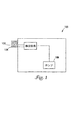
図1は、メモリカード100の一実施形態を示す。メモリカード100は、デジタルカメラ、プリンタ、携帯電話などの機器に対するメモリカード100の接続に用いる複数のピンを備える。メモリカード100は、標準的なピン配置を有するものであり、余分な電力効率(extra power efficiencies)を有さないシステムに使用可能である。標準的なピン配置のうち、参照符号102、104が付された2本のピンは、標準的なメモリカードにおける従来の「無接続」ピンである。しかし、メモリカード100において、これらのピン102、104は、標準的でない電圧をカードに使用して、メモリカード100の内部電圧ポンプ106の効率を増加するか否かを検出する検出回路に内部で接続されている。
FIG. 1 shows an embodiment of a
例えば、1.6ボルトで動作するが、より高い電圧(例えば、3.0ボルト)で動作する液晶表示ディスプレイ(LCD)などを有する携帯電話のメモリに、メモリカード100が使用されている場合、このより高い電圧は、様々な実施形態において内部ポンプに供給され、この内部ポンプは、メモリ又はメモリカードをより効率的にする。或いは、より高い電圧が、2本のピン102、104の一方を介して供給される一方、外部電圧を使用するか否かを示す信号が、ピン102、104の他方に供給される。
For example, when the
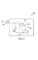
図2は、別の実施形態に係るメモリカード200を示す。メモリカード200は、標準的なメモリカードでも機能するピン配置を有する。追加のピン202は、標準的な構成において「無接続」ピンであるが、本実施形態では、メモリカード200のポンプ構成の電力効率を変更するのに用いられる。この実施形態では、メモリカード200が、ポンプ効率の向上に利用可能な何らかの外部電源、外部インダクタ若しくはこれらの組合せに接続されているか否か、又は、標準的な内部ポンプ構成を用いるべきか否かをハードウェア検出機構206を用いて検出する。
FIG. 2 shows a
一実施形態において、ハードウェア検出システム206は、一対のトランジスタ208、210とプルダウン抵抗212を備える。プルダウン抵抗212を設けることは、任意である。ハードウェア検出システム206は、ピン202に接続され、このピン202には、外部電圧を接続可能である。ピン202は、プルダウン抵抗212を介してノード214に接続される。ノード214は、n型トランジスタ208のゲート及びp型トランジスタ210のゲートに接続される。外部電圧機器がピン202に接続されていない場合、又は、ピン202の電圧が変動(floating)している場合、ノード214の電圧は、プルダウン抵抗212を介して略ゼロになり、外部機器がピン202に接続されていないことを示す。この場合、トランジスタ210がオンとなり、トランジスタ208がオフとなり、電源電圧Vccがポンプ216に印加されるため、メモリカード200は、内部電圧Vccで動作する。ピン202に外部電圧が印加されている場合、ノード214における電圧が、トランジスタ210をオフとし、トランジスタ208をオンとするのに十分な高さになると、ピン202における電圧はポンプ216に供給される。
In one embodiment, the
上述のハードウェア検出機構206を変化させて、いずれの電圧を内部ポンプ216に印加するかを制御することが容易であることが理解されよう。また、メモリやメモリカードによっては、3つ以上の電圧を選択的に内部ポンプに接続可能であり、さらに、別の実施形態として、複数のポテンシャル電圧(potential voltages)を検出し、ポンプの作動のために最も高い電圧又は最も適切な電圧をポンプに印加可能であることも理解されよう。ポンプに印加される電圧の選択は、ハードウェア、ファームウェア、ソフトウェアを介する実施形態、又はメモリコントローラにより供給されるコマンド信号を用いる実施形態など様々な実施形態により行うことができる。本実施形態のハードウェア検出機構206は、別のピン上の外部インダクタの存在も検出可能であり、また、機器の動作を再設定し、外部インダクタのみの使用又は外部電圧と組み合わせての外部インダクタの使用により、より高い効率を実現する。一実施形態において、外部電圧及び外部インダクタの両方が検出された場合、外部電圧は、内部電圧ポンプの効率を向上させるのに用いられ、外部インダクタは、昇圧された電圧を用いてさらに効率を向上させる。
It will be appreciated that it is easy to control which voltage is applied to the
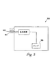
図3に示す別の実施形態300において、外部ピン302は、検出機構としてのみ用いられ、ピン304は、外部電圧又はインダクタに接続される。この実施形態において、内部ポンプ306を用いる場合、メモリカード300は、検出ピン302をLo信号とする。この実施形態では、ピン304に接続するものとして2つの外部機器が選択可能である。選択可能な2つの外部機器の一方が使用される場合、メモリカード300は、ピン302にHi信号を接続する。そして、メモリは、検出ピン302におけるHi信号から何らかの外部補助装置が使用されることを認識する。次いで、電圧検出機構を用いて、ピン304に接続される補助機器の種類を判定する。
In another
Hi信号を検出した場合、電圧検出機構は、ピン304に電源が接続されたと判定し、ピン304を新たな電源として用いてポンプ306をより効率化し、メモリカード300の電力性能を向上させる。ピン304にインダクタが接続されている場合、検出される電圧はなく、メモリは、ピン304にインダクタが接続されていると判定する。本実施形態に係るメモリデバイスは、ポンプ306を再構成して、内部ポンプの代わりにインダクタを用い、システムの電力効率をより高いものにする。別の実施形態として、インダクタを介して内部ポンプを作動させることもできる。さらに別の実施形態として、電源電圧よりも高い内部電圧と共に外部インダクタを用いることもできる。
When the Hi signal is detected, the voltage detection mechanism determines that a power source is connected to the
さらに別の実施形態として、2本の従来の「無接続」ピンに、外部電圧を印加し、外部インダクタを接続することもできる。メモリは、標準的なピン配置を有し、従来のシステムにおいて接続されるとき、スタンドアロン型の従来式メモリとして動作する。外部ピンにおいて何らかの存在を検出したとき、デバイスは、個々の構成要素それぞれに対して上述のように接続された外部素子を用いて動作する。しかし、外部インダクタと外部電源の両方がそれらのピンに接続されたとき、両方が使用される。一実施形態において、外部電圧が内部ポンプに印加され、より高効率の昇圧電圧が供給される。そして、その昇圧電圧は、外部インダクタを介してより高効率の動作を可能にする。 As yet another embodiment, an external voltage can be applied to two conventional “no connection” pins to connect an external inductor. The memory has a standard pinout and operates as a stand-alone conventional memory when connected in a conventional system. When detecting any presence at an external pin, the device operates with external elements connected as described above for each individual component. However, when both an external inductor and an external power supply are connected to their pins, both are used. In one embodiment, an external voltage is applied to the internal pump to provide a more efficient boosted voltage. The boosted voltage enables a more efficient operation via the external inductor.
本発明に係る実施形態では、標準的なピン配置を有するメモリを用いるが、この標準的なピン配置は、メモリをより高効率に動作させる付加的な特徴を有する。但し、外部電圧又は他の電圧供給要素がシステムに接続されているとき、その標準的な特徴は失われない。 Embodiments according to the present invention use a memory with a standard pinout, but this standard pinout has the additional feature of operating the memory more efficiently. However, when an external voltage or other voltage supply element is connected to the system, its standard features are not lost.
上述したメモリカードの各種構成では、メモリカードが従来の2本の余分な「無接続」ピンを備える標準的なピン構成を有する場合、上述のようにプルダウン抵抗を用いることができる。システムにプルアップピンが存在する場合、プルダウン抵抗に接続されているそのプルアップピンは、メモリ内部においてLoとされ、メモリカードが、他のNAND型メモリカードと同様に通常モードで動作する。メモリカードは、通常のピン配置を用いて動作するため、内部ポンプ用の高電圧電源を用いるようには構成されていない標準的なシステムで用いることができる。2本の余分なピンは、システムにおける「無接続」ピンである。しかし、外部電源又は別の内部電源を用いるように構成されたシステムでは、メモリカードをそのように用いることができる。 In the various configurations of the memory card described above, a pull-down resistor can be used as described above when the memory card has a standard pin configuration with two conventional “no connection” pins. When there is a pull-up pin in the system, the pull-up pin connected to the pull-down resistor is set to Lo in the memory, and the memory card operates in the normal mode like other NAND type memory cards. Since the memory card operates using a normal pinout, it can be used in a standard system that is not configured to use a high voltage power supply for the internal pump. The two extra pins are “no connection” pins in the system. However, in a system configured to use an external power supply or another internal power supply, a memory card can be used as such.
或いは、単一の外部電力補助機構又は電圧をピン304に接続し、そして、検出ピン302がHi信号にされると、ピン304に接続された単一の外部電力補助機構を用いてポンプ306の初期電圧を供給する。
Alternatively, when a single external power assist mechanism or voltage is connected to pin 304 and the
動作に影響する構成要素は、メモリやメモリカードの標準的な構成における「無接続」ピンにのみ接続されるため、本発明に係る実施形態は、標準的なシステムに接続することが可能であり、また、標準的なシステムにおいて動作することができる。コマンドや指示がメモリやメモリカードに送信された場合、又は外部電圧が各種実施形態のピンに接続又は検出された場合のみ、当該動作が新たなモードで開始される。 Since the components that affect operation are connected only to the “no connection” pins in the standard configuration of memory and memory cards, embodiments according to the present invention can be connected to a standard system. Can also operate in a standard system. The operation is started in a new mode only when a command or instruction is transmitted to a memory or a memory card, or when an external voltage is connected or detected to a pin of various embodiments.
本発明に係る実施形態のいずれにおいても、本発明の範囲から逸脱することなしに、外部補助装置及び内部電源電圧Vccの組合せを用いることができる。別の実施形態において、電源電圧Vccよりも高い電圧を発生させ、メモリカード100、200、又は300などのメモリカードを使用可能なシステムの他の構成要素を動作させることができる。そのような別の電圧には、例えば、ディスプレイスクリーン用電圧、内部バッテリ供給電力などが含まれる。そのような構成では、本発明に係る実施形態及び回路を変形し、他の内部電圧を内部ポンプに印加すること、又は外部から接続されたインダクタを他の内部電圧と組み合わせて用いることは単純な事柄である。そのような変形は、当業者に理解可能であり、本発明及びその実施形態の範囲に含まれる。
In any of the embodiments according to the present invention, a combination of the external auxiliary device and the internal power supply voltage Vcc can be used without departing from the scope of the present invention. In another embodiment, a voltage higher than the power supply voltage Vcc can be generated to operate other components of the system that can use the memory card, such as the
本発明の各種実施形態に係るメモリデバイスは、初期セットアップ時におけるコントローラからのコマンドを介して構成を変更可能である。別の実施形態において、このコマンドは、書込み処理又は消去処理の直前に供給することもできる。一実施形態において、メモリデバイスは、コマンドに応じて、メモリカード外部からの電源を用い、又は内部ポンプの代わりに、外部から接続されたインダクタを用いることができる。 The configuration of the memory device according to various embodiments of the present invention can be changed through a command from the controller during initial setup. In another embodiment, this command may be supplied immediately before the write or erase process. In one embodiment, the memory device can use an external power supply in response to a command, or can use an externally connected inductor instead of an internal pump.
本発明に係るさらに別の実施形態は、上記コンセプトを用いるメモリデバイスを有する。例えば、図4には、本発明に係る実施形態を用いるのに適したメモリが示されている。図4は、本発明の一実施形態としてのメモリデバイス400(例えば、フラッシュメモリデバイス)の機能ブロック図であり、このメモリデバイス400は、プロセッサ410に接続されている。メモリデバイス400及びプロセッサ410は、電子システム420の一部を構成する。メモリデバイス400は、本発明の理解を容易化するためにメモリの特徴に焦点を当てるように簡略化されている。メモリデバイス400は、メモリセルのアレイ430を有する。メモリアレイ430は、行及び列のバンク単位で構成されている。
Yet another embodiment according to the invention comprises a memory device using the above concept. For example, FIG. 4 shows a memory suitable for using an embodiment according to the present invention. FIG. 4 is a functional block diagram of a memory device 400 (eg, a flash memory device) as an embodiment of the present invention, and the
アドレス入力端子A0−Ax442に供給されたアドレス信号をラッチするため、アドレスバッファ回路440が設けられている。アドレス信号は、メモリアレイ430にアクセスするため、行デコーダ444及び列レコーダ446により受信及びデコードされる。当業者であれば、本願の開示に基づけば、アドレス入力端子の数が、メモリアレイの密度や構造に依存することを理解できるであろう。すなわち、アドレスの数は、メモリセルの数並びにバンク及びブロックの数が増加するにつれて増える。
An
メモリデバイス400は、検出/ラッチ回路450を用いてメモリアレイ430の列における電圧又は電流の変化を検出することにより、メモリアレイ430のデータを読み出す。一実施形態において、検出/ラッチ回路450は、メモリアレイ430からのデータ列を読み出し、これをラッチすることができるように接続されている。複数のデータ(DQ)端子462を介してプロセッサ410と双方向にデータ通信をするために、データ入出力バッファ回路460が設けられている。また、このデータ入出力バッファ回路460は、メモリ400において読出し処理及び書込み処理を行うために、書込み回路455及び読出し/ラッチ回路450に接続されている。プロセッサ410から制御端子472を介して供給された信号は、コマンド制御回路470によりデコードされる。これらの信号は、データ読出し処理、データ書込み処理、及び消去処理を含むメモリアレイ430に対する処理を制御するために用いられる。フラッシュメモリデバイスは、メモリの特徴に関する基本的な理解を促進するために簡略化されている。内部回路及びフラッシュメモリの機能の詳細は、当業者にとって周知であろう。一実施形態において、検出回路490を用いて、内部電圧ポンプ(図示せず)を用いるか否か、又は本発明に係る各種実施形態について上述したような外部電源又はインダクタを用いるか否かを検出する。上述した実施形態は、図4に示す基礎的なメモリアレイ又はシステム構造における各実施形態において用いられる。
The
結び
本発明の各種実施形態は、無接続ピンを介して外部電圧を供給する外部機器、又は標準的な機器として使用可能なものの有無を検出し、この検出結果に基づいて内部電圧ポンプの構成を変更させる内部検出機構を備えるメモリを有する。本実施形態により、システムにおける他の電源の利用可能性に応じて、又は、インダクタなど利用可能な機器に応じてカードの電力消費を減少させ、内部電圧をより効率的に供給する。
Conclusion Various embodiments of the present invention detect the presence of an external device that supplies an external voltage via a non-connecting pin, or a device that can be used as a standard device, and configure the configuration of the internal voltage pump based on the detection result. A memory having an internal detection mechanism to be changed; According to the present embodiment, the power consumption of the card is reduced according to the availability of other power sources in the system or according to available devices such as inductors, thereby supplying the internal voltage more efficiently.
ここでは、具体的な実施形態について説明してきたが、当該分野の当業者にとって、上記の実施形態に代えて、同一の目的を達成することのできるあらゆる構成が利用可能である。本願は、本発明に関するあらゆる応用及び改変を包含することを意図している。従って、本発明が添付の特許請求の範囲及びその均等の範囲によってのみ限定されることを明確に意図している。 Although specific embodiments have been described here, any configuration that can achieve the same object can be used by those skilled in the art instead of the above-described embodiments. This application is intended to cover any applications and variations relating to the present invention. Therefore, it is manifestly intended that this invention be limited only by the claims appended hereto and their equivalents.
Claims (10)
メモリセルのアレイと、
前記メモリセルに対する読出し処理、書込み処理及び消去処理を行う制御回路と、
アドレス信号を受信するアドレス入力端子と、
前記アドレス入力端子に接続され前記アドレス信号をラッチするアドレス回路と、
前記メモリデバイスにおける内部電源電圧の代わりに当該内部電源電圧よりも高い電圧を前記メモリデバイスに供給する内部電圧ポンプと、
前記第1動作モードで用いる第1接続ピンと、
前記第1接続ピンと同一のピン配列に含まれ、前記第2動作モードで用いるが前記第1動作モードで用いない第2接続ピンと、
前記第2接続ピンに接続され、前記第2接続ピンに外部電源が接続されたとき、前記外部電源からの外部電圧を前記内部電圧ポンプに昇圧させる検出機構と
を備える
ことを特徴とするメモリデバイス。 A memory device operable in a first operation mode that operates at a relatively low voltage and a second operation mode that operates at a relatively high voltage ,
An array of memory cells;
A control circuit for performing a read process, a write process, and an erase process on the memory cell;
An address input terminal for receiving an address signal;
An address circuit connected to the address input terminal and latching the address signal;
An internal voltage pump for supplying a voltage higher than the internal power supply voltage to the memory device instead of the internal power supply voltage in the memory device;
A first connection pin used in the first operation mode;
A second connection pin that is included in the same pin arrangement as the first connection pin and is used in the second operation mode but not in the first operation mode;
It is connected to the second connecting pin, when said external power source is connected to the second connecting pin, a memory, characterized in that Ru and a detecting mechanism for boosting the external voltage from the external power source to the internal voltage pump device.
前記検出機構は、
前記第2接続ピンに接続され、前記第2接続ピンに前記外部電源が接続されていないとき、前記内部電圧ポンプに対する前記内部電源電圧を通過させるp型の第1トランジスタゲートと、
前記第2接続ピンに接続され、前記第2接続ピンに前記外部電源が接続されているとき、前記内部電圧ポンプに対する前記外部電源からの外部電圧を通過させるn型の第2トランジスタゲートと、
を有することを特徴とするメモリデバイス。The memory device of claim 1, wherein
The detection mechanism is:
Is connected to the second connecting pin, and wherein when the external power source is not connected to the second connection pin, the first transistor gate of the p-type passing said internal power supply voltage to the internal voltage pump,
Is connected to the second connecting pin, and wherein when the external power source is connected to the second connection pin, the second transistor gate of n-type to pass the external voltage from the external power source to the internal voltage pump,
A memory device comprising:
前記第2トランジスタゲートは、前記内部電圧ポンプに対する前記外部電圧が前記内部電源電圧を越えたとき、前記内部電圧ポンプに対する前記外部電圧のみを通過させる
ことを特徴とするメモリデバイス。The memory device of claim 2, wherein
Said second transistor gate, when said external voltage exceeds the internal power supply voltage, a memory device, characterized in that passing only the external voltage to the internal voltage pump to said internal voltage pump.
前記第2接続ピンと前記第1及び第2トランジスタゲートとの間に接続された抵抗をさらにする
ことを特徴とするメモリデバイス。The memory device according to claim 2 or 3 ,
Memory device characterized by further a resistor connected between the second connecting pin and the first and second transistor gates.
前記第2接続ピンを複数備え、
前記第2接続ピンのうち第1ピンは、イネーブル信号を受信可能であり、
前記第2接続ピンのうち第2ピンは、前記外部電源に接続可能であり、
前記イネーブル信号の電圧レベルは、前記内部電源電圧又は前記第2ピンに接続された前記外部電源からの外部電圧を用いるかどうかをイネーブルする
ことを特徴とするメモリデバイス。The memory device according to any one of claims 1 to 4 ,
A plurality of the second connection pins;
The first pin of the second connection pins can receive an enable signal;
Second pin of the second connecting pin is connectable to the external power supply,
The voltage level of the enable signal, a memory device, wherein the enabling whether using an external voltage from the internal power supply voltage or said external power source connected to the second pin.
前記メモリデバイスは、メモリカード内に設けられている
ことを特徴とするメモリデバイス。In the memory device according to any one of claims 1 to 5,
The memory device includes a memory device, characterized in that provided in the memory card.
前記メモリデバイスは、前記メモリデバイスに接続されたマイクロプロセッサを有するシステムに設けられている
ことを特徴とするメモリデバイス。The memory device according to any one of claims 1 to 6 ,
The memory device is provided in a system having a microprocessor connected to the memory device.
前記メモリカードは、前記第1動作モードで用いる第1接続ピンと、前記第1接続ピンと同一のピン配列に含まれ、前記第2動作モードで用いるが前記第1動作モードで用いない第2接続ピンとを備え、
外部電源が前記第2接続ピンに接続されていないとき、内部電源電圧を内部電圧ポンプで昇圧する前記第1動作モードで前記メモリカードを動作させるステップと、
前記外部電源が前記第2接続ピンに接続されているとき、前記外部電源からの外部電圧を前記内部電圧ポンプで昇圧する前記第2動作モードで前記メモリカードを動作させるステップと、
を有するメモリカード動作方法。A memory card operation method for operating a memory card operable in a first operation mode that operates at a relatively low voltage and a second operation mode that operates at a relatively high voltage ,
The memory card includes a first connection pin used in the first operation mode, and a second connection pin included in the same pin arrangement as the first connection pin and used in the second operation mode but not used in the first operation mode. With
When the external power supply is not connected to the second connecting pin, and the step of operating the memory card in the first operation mode for boosting by the internal voltage pump to the internal power supply voltage,
Operating the memory card in the second operation mode in which the external voltage from the external power supply is boosted by the internal voltage pump when the external power supply is connected to the second connection pin ;
A memory card operating method.
前記外部電圧又は前記内部電源電圧のいずれを用いるかを検出回路を用いて検出するステップをさらに有する
ことを特徴とするメモリカード動作方法。The memory card operating method according to claim 8 ,
Memory card operation method characterized by further comprising the step of detecting using detecting circuit whether to use any of the external voltage or the internal power supply voltage.
前記検出回路を用いて検出するステップは、
前記第2接続ピンの電圧レベルを監視するステップと、
前記第2接続ピンの電圧が、前記内部電源電圧を越えたとき、前記第1動作モードから前記第2動作モードに切り替えるステップと、
を有することを特徴とするメモリカード動作方法。The memory card operating method according to claim 9 , wherein
The step of detecting using the detection circuit comprises:
Monitoring the voltage level of the second connection pin;
When the voltage of the second connecting pin, which exceeds the internal power supply voltage, a step of switching from the first operation mode to the second operation mode,
A memory card operating method characterized by comprising:
Applications Claiming Priority (3)
| Application Number | Priority Date | Filing Date | Title |
|---|---|---|---|
| US10/930,524 | 2004-08-31 | ||
| US10/930,524 US7196958B2 (en) | 2004-08-31 | 2004-08-31 | Power efficient memory and cards |
| PCT/US2005/030036 WO2006026282A1 (en) | 2004-08-31 | 2005-08-24 | Power efficient memory and cards |
Publications (2)
| Publication Number | Publication Date |
|---|---|
| JP2008511921A JP2008511921A (en) | 2008-04-17 |
| JP4843796B2 true JP4843796B2 (en) | 2011-12-21 |
Family
ID=35478684
Family Applications (1)
| Application Number | Title | Priority Date | Filing Date |
|---|---|---|---|
| JP2007530066A Expired - Fee Related JP4843796B2 (en) | 2004-08-31 | 2005-08-24 | High power efficiency memory and card |
Country Status (9)
| Country | Link |
|---|---|
| US (2) | US7196958B2 (en) |
| EP (1) | EP1784832B1 (en) |
| JP (1) | JP4843796B2 (en) |
| KR (1) | KR100904341B1 (en) |
| CN (1) | CN101031976B (en) |
| AT (1) | ATE426896T1 (en) |
| DE (1) | DE602005013534D1 (en) |
| TW (1) | TWI313873B (en) |
| WO (1) | WO2006026282A1 (en) |
Families Citing this family (10)
| Publication number | Priority date | Publication date | Assignee | Title |
|---|---|---|---|---|
| US7196958B2 (en) * | 2004-08-31 | 2007-03-27 | Micron Technology, Inc. | Power efficient memory and cards |
| WO2006057049A1 (en) | 2004-11-26 | 2006-06-01 | Kabushiki Kaisha Toshiba | Card and host device |
| US8060142B2 (en) * | 2006-05-24 | 2011-11-15 | Lg Electronics Inc. | Method for reducing power consumption for detachable card and mobile communication terminal thereof |
| US7512029B2 (en) * | 2006-06-09 | 2009-03-31 | Micron Technology, Inc. | Method and apparatus for managing behavior of memory devices |
| US8615467B2 (en) | 2007-11-07 | 2013-12-24 | International Business Machines Corporation | Electronic system for selecting the best card from a collection of consumer credit, debit, and discount cards |
| JP5386931B2 (en) * | 2007-11-15 | 2014-01-15 | 株式会社リコー | Memory card control device and memory card control method |
| CN102395988B (en) * | 2009-04-27 | 2015-04-29 | 日本电气株式会社 | Card device and method for supplying the card device with power |
| TWI416313B (en) * | 2009-07-31 | 2013-11-21 | Via Tech Inc | Power-saving computer system and the method thereof, and power-saving power management unit |
| KR102133955B1 (en) | 2019-04-23 | 2020-07-15 | 주식회사 에프이씨 | Personal transportation device having steering function |
| KR102133962B1 (en) | 2019-04-23 | 2020-07-15 | 주식회사 에프이씨 | Wireless controlled personal transportation system |
Family Cites Families (36)
| Publication number | Priority date | Publication date | Assignee | Title |
|---|---|---|---|---|
| US5019772A (en) * | 1989-05-23 | 1991-05-28 | International Business Machines Corporation | Test selection techniques |
| JP2923985B2 (en) | 1989-07-26 | 1999-07-26 | 日本電気株式会社 | EEPROM device |
| US5291584A (en) * | 1991-07-23 | 1994-03-01 | Nexcom Technology, Inc. | Methods and apparatus for hard disk emulation |
| US5267218A (en) * | 1992-03-31 | 1993-11-30 | Intel Corporation | Nonvolatile memory card with a single power supply input |
| JP3053301B2 (en) * | 1992-09-11 | 2000-06-19 | 三菱電機株式会社 | Semiconductor integrated circuit and IC card |
| US5530640A (en) * | 1992-10-13 | 1996-06-25 | Mitsubishi Denki Kabushiki Kaisha | IC substrate and boosted voltage generation circuits |
| US5664231A (en) * | 1994-04-29 | 1997-09-02 | Tps Electronics | PCMCIA interface card for coupling input devices such as barcode scanning engines to personal digital assistants and palmtop computers |
| US5594360A (en) * | 1994-10-19 | 1997-01-14 | Intel Corporation | Low current reduced area programming voltage detector for flash memory |
| EP0792505B1 (en) * | 1994-10-19 | 2001-07-04 | Intel Corporation | Voltage supplies for flash memory |
| US5483486A (en) * | 1994-10-19 | 1996-01-09 | Intel Corporation | Charge pump circuit for providing multiple output voltages for flash memory |
| US5495453A (en) * | 1994-10-19 | 1996-02-27 | Intel Corporation | Low power voltage detector circuit including a flash memory cell |
| US5671179A (en) * | 1994-10-19 | 1997-09-23 | Intel Corporation | Low power pulse generator for smart voltage flash eeprom |
| US5651011A (en) * | 1995-06-01 | 1997-07-22 | Micron Technology, Inc. | Method and apparatus for initiating and controlling test modes within an integrated circuit |
| US5657284A (en) * | 1995-09-19 | 1997-08-12 | Micron Technology, Inc. | Apparatus and method for testing for defects between memory cells in packaged semiconductor memory devices |
| US5965902A (en) * | 1995-09-19 | 1999-10-12 | Micron Technology | Method and apparatus for testing of dielectric defects in a packaged semiconductor memory device |
| KR0179852B1 (en) * | 1995-10-25 | 1999-04-15 | 문정환 | Charge pumping circuit |
| US5874849A (en) * | 1996-07-19 | 1999-02-23 | Texas Instruments Incorporated | Low voltage, high current pump for flash memory |
| US6037792A (en) * | 1996-12-21 | 2000-03-14 | Stmicroelectronics, Inc. | Burn-in stress test mode |
| US5991851A (en) * | 1997-05-02 | 1999-11-23 | Enhanced Memory Systems, Inc. | Enhanced signal processing random access memory device utilizing a DRAM memory array integrated with an associated SRAM cache and internal refresh control |
| US6154851A (en) * | 1997-08-05 | 2000-11-28 | Micron Technology, Inc. | Memory repair |
| US6208542B1 (en) * | 1998-06-30 | 2001-03-27 | Sandisk Corporation | Techniques for storing digital data in an analog or multilevel memory |
| KR100272511B1 (en) * | 1998-08-10 | 2000-11-15 | 김영환 | High voltage generation circuit in semiconductor memory devices |
| US6166961A (en) * | 1999-08-19 | 2000-12-26 | Aplus Flash Technology, Inc. | Approach to provide high external voltage for flash memory erase |
| FR2800214B1 (en) * | 1999-10-22 | 2001-12-28 | St Microelectronics Sa | CHARGE PUMP TYPE VOLTAGE LIFTING CIRCUIT |
| US7073014B1 (en) | 2000-07-28 | 2006-07-04 | Micron Technology, Inc. | Synchronous non-volatile memory system |
| US6469474B2 (en) * | 2000-09-08 | 2002-10-22 | Compaq Information Technologies Group, L.P. | Battery gauge using a resettable decrementer in a DIMM |
| US6515901B2 (en) * | 2000-12-29 | 2003-02-04 | Intel Corporation | Method and apparatus for allowing continuous application of high voltage to a flash memory device power pin |
| JP2002296515A (en) * | 2001-03-30 | 2002-10-09 | Ngk Insulators Ltd | Optical system of display |
| JP2003085484A (en) * | 2001-09-11 | 2003-03-20 | Ricoh Co Ltd | Ic card system |
| JP3883126B2 (en) * | 2001-10-26 | 2007-02-21 | 富士通株式会社 | Semiconductor integrated circuit device, electronic device incorporating the same, and power consumption reduction method |
| JP2003187596A (en) * | 2001-12-14 | 2003-07-04 | Mitsubishi Electric Corp | Semiconductor memory |
| JP2003208794A (en) * | 2002-01-10 | 2003-07-25 | Seiko Epson Corp | Nonvolatile semiconductor memory device |
| JP2003316664A (en) * | 2002-04-24 | 2003-11-07 | Mitsubishi Electric Corp | Nonvolatile semiconductor storage device |
| JP4133166B2 (en) * | 2002-09-25 | 2008-08-13 | 株式会社ルネサステクノロジ | Nonvolatile semiconductor memory device |
| US6870774B2 (en) * | 2002-12-10 | 2005-03-22 | Micron, Technology, Inc. | Flash memory architecture for optimizing performance of memory having multi-level memory cells |
| US7196958B2 (en) * | 2004-08-31 | 2007-03-27 | Micron Technology, Inc. | Power efficient memory and cards |
-
2004
- 2004-08-31 US US10/930,524 patent/US7196958B2/en not_active Expired - Fee Related
-
2005
- 2005-08-24 KR KR1020077007576A patent/KR100904341B1/en not_active IP Right Cessation
- 2005-08-24 DE DE602005013534T patent/DE602005013534D1/en active Active
- 2005-08-24 WO PCT/US2005/030036 patent/WO2006026282A1/en active Application Filing
- 2005-08-24 CN CN200580033210XA patent/CN101031976B/en not_active Expired - Fee Related
- 2005-08-24 JP JP2007530066A patent/JP4843796B2/en not_active Expired - Fee Related
- 2005-08-24 AT AT05790390T patent/ATE426896T1/en not_active IP Right Cessation
- 2005-08-24 EP EP05790390A patent/EP1784832B1/en not_active Not-in-force
- 2005-08-26 TW TW094129263A patent/TWI313873B/en not_active IP Right Cessation
-
2007
- 2007-03-27 US US11/691,817 patent/US7483330B2/en not_active Expired - Fee Related
Also Published As
| Publication number | Publication date |
|---|---|
| KR20070054718A (en) | 2007-05-29 |
| US7483330B2 (en) | 2009-01-27 |
| US7196958B2 (en) | 2007-03-27 |
| US20060044887A1 (en) | 2006-03-02 |
| JP2008511921A (en) | 2008-04-17 |
| TWI313873B (en) | 2009-08-21 |
| KR100904341B1 (en) | 2009-06-23 |
| CN101031976A (en) | 2007-09-05 |
| EP1784832B1 (en) | 2009-03-25 |
| TW200623142A (en) | 2006-07-01 |
| WO2006026282A1 (en) | 2006-03-09 |
| CN101031976B (en) | 2010-05-26 |
| DE602005013534D1 (en) | 2009-05-07 |
| US20070189099A1 (en) | 2007-08-16 |
| ATE426896T1 (en) | 2009-04-15 |
| EP1784832A1 (en) | 2007-05-16 |
Similar Documents
| Publication | Publication Date | Title |
|---|---|---|
| JP4843796B2 (en) | High power efficiency memory and card | |
| US7916557B2 (en) | NAND interface | |
| TWI669714B (en) | Voltage control device and memory system | |
| US8923088B2 (en) | Solid state storage device with sleep control circuit | |
| US7304891B2 (en) | Apparatus and method for improving write/read endurance of non-volatile memory | |
| EP1469480A2 (en) | Non-volatile semiconductor memory device, electronic card using the same and electronic apparatus | |
| US20060085583A1 (en) | Multi-functional integrated circuit card module with a mixed interface | |
| KR102142790B1 (en) | Semiconductor storage device | |
| EP1513070B1 (en) | System having insertable and removable storage and a control method thereof | |
| US7626865B2 (en) | Charge pump operation in a non-volatile memory device | |
| CN113924624A (en) | Memory device including voltage generation system | |
| CN107017024B (en) | Semiconductor device and semiconductor integrated circuit | |
| CN111402943B (en) | Method, system, storage medium and terminal for reducing area of read operation pump of non-flash memory | |
| JP2011108349A (en) | Semiconductor memory device | |
| US20060236164A1 (en) | Automatic test entry termination in a memory device | |
| CN115808964A (en) | Memory, memory control method and system | |
| JP2005234935A (en) | Information storage device | |
| US7742346B2 (en) | Voltage booster and memory structure using the same | |
| JP2006185530A (en) | Nonvolatile semiconductor memory device | |
| CN112837719A (en) | Memory device and method for assisting read operation in memory device | |
| US7978002B2 (en) | Voltage boosting circuit and semiconductor device | |
| JP2001075745A (en) | Information processor and adaptor for fitting semiconductor memory | |
| JP2005251278A (en) | Ferroelectric memory device and electronic equipment |
Legal Events
| Date | Code | Title | Description |
|---|---|---|---|
| A977 | Report on retrieval |
Free format text: JAPANESE INTERMEDIATE CODE: A971007 Effective date: 20100106 |
|
| A131 | Notification of reasons for refusal |
Free format text: JAPANESE INTERMEDIATE CODE: A131 Effective date: 20100119 |
|
| A601 | Written request for extension of time |
Free format text: JAPANESE INTERMEDIATE CODE: A601 Effective date: 20100416 |
|
| A602 | Written permission of extension of time |
Free format text: JAPANESE INTERMEDIATE CODE: A602 Effective date: 20100423 |
|
| A601 | Written request for extension of time |
Free format text: JAPANESE INTERMEDIATE CODE: A601 Effective date: 20100518 |
|
| A602 | Written permission of extension of time |
Free format text: JAPANESE INTERMEDIATE CODE: A602 Effective date: 20100525 |
|
| A601 | Written request for extension of time |
Free format text: JAPANESE INTERMEDIATE CODE: A601 Effective date: 20100618 |
|
| A602 | Written permission of extension of time |
Free format text: JAPANESE INTERMEDIATE CODE: A602 Effective date: 20100625 |
|
| A521 | Request for written amendment filed |
Free format text: JAPANESE INTERMEDIATE CODE: A523 Effective date: 20100720 |
|
| A131 | Notification of reasons for refusal |
Free format text: JAPANESE INTERMEDIATE CODE: A131 Effective date: 20101116 |
|
| A601 | Written request for extension of time |
Free format text: JAPANESE INTERMEDIATE CODE: A601 Effective date: 20110216 |
|
| A602 | Written permission of extension of time |
Free format text: JAPANESE INTERMEDIATE CODE: A602 Effective date: 20110223 |
|
| A601 | Written request for extension of time |
Free format text: JAPANESE INTERMEDIATE CODE: A601 Effective date: 20110316 |
|
| A602 | Written permission of extension of time |
Free format text: JAPANESE INTERMEDIATE CODE: A602 Effective date: 20110324 |
|
| A521 | Request for written amendment filed |
Free format text: JAPANESE INTERMEDIATE CODE: A523 Effective date: 20110418 |
|
| A01 | Written decision to grant a patent or to grant a registration (utility model) |
Free format text: JAPANESE INTERMEDIATE CODE: A01 Effective date: 20110719 |
|
| A01 | Written decision to grant a patent or to grant a registration (utility model) |
Free format text: JAPANESE INTERMEDIATE CODE: A01 |
|
| A601 | Written request for extension of time |
Free format text: JAPANESE INTERMEDIATE CODE: A601 Effective date: 20110818 |
|
| A602 | Written permission of extension of time |
Free format text: JAPANESE INTERMEDIATE CODE: A602 Effective date: 20110823 |
|
| A711 | Notification of change in applicant |
Free format text: JAPANESE INTERMEDIATE CODE: A711 Effective date: 20110915 |
|
| A61 | First payment of annual fees (during grant procedure) |
Free format text: JAPANESE INTERMEDIATE CODE: A61 Effective date: 20110915 |
|
| A521 | Request for written amendment filed |
Free format text: JAPANESE INTERMEDIATE CODE: A821 Effective date: 20110915 |
|
| FPAY | Renewal fee payment (event date is renewal date of database) |
Free format text: PAYMENT UNTIL: 20141021 Year of fee payment: 3 |
|
| R150 | Certificate of patent or registration of utility model |
Free format text: JAPANESE INTERMEDIATE CODE: R150 |
|
| R250 | Receipt of annual fees |
Free format text: JAPANESE INTERMEDIATE CODE: R250 |
|
| R250 | Receipt of annual fees |
Free format text: JAPANESE INTERMEDIATE CODE: R250 |
|
| LAPS | Cancellation because of no payment of annual fees |