JP4843248B2 - Improved pattern definition apparatus for particle beam exposure. - Google Patents
Improved pattern definition apparatus for particle beam exposure. Download PDFInfo
- Publication number
- JP4843248B2 JP4843248B2 JP2005134248A JP2005134248A JP4843248B2 JP 4843248 B2 JP4843248 B2 JP 4843248B2 JP 2005134248 A JP2005134248 A JP 2005134248A JP 2005134248 A JP2005134248 A JP 2005134248A JP 4843248 B2 JP4843248 B2 JP 4843248B2
- Authority
- JP
- Japan
- Prior art keywords
- blank
- line
- group
- aperture
- apertures
- Prior art date
- Legal status (The legal status is an assumption and is not a legal conclusion. Google has not performed a legal analysis and makes no representation as to the accuracy of the status listed.)
- Expired - Fee Related
Links
Images


Classifications
-
- B—PERFORMING OPERATIONS; TRANSPORTING
- B82—NANOTECHNOLOGY
- B82Y—SPECIFIC USES OR APPLICATIONS OF NANOSTRUCTURES; MEASUREMENT OR ANALYSIS OF NANOSTRUCTURES; MANUFACTURE OR TREATMENT OF NANOSTRUCTURES
- B82Y10/00—Nanotechnology for information processing, storage or transmission, e.g. quantum computing or single electron logic
-
- G—PHYSICS
- G21—NUCLEAR PHYSICS; NUCLEAR ENGINEERING
- G21K—TECHNIQUES FOR HANDLING PARTICLES OR IONISING RADIATION NOT OTHERWISE PROVIDED FOR; IRRADIATION DEVICES; GAMMA RAY OR X-RAY MICROSCOPES
- G21K1/00—Arrangements for handling particles or ionising radiation, e.g. focusing or moderating
- G21K1/08—Deviation, concentration or focusing of the beam by electric or magnetic means
-
- B—PERFORMING OPERATIONS; TRANSPORTING
- B82—NANOTECHNOLOGY
- B82Y—SPECIFIC USES OR APPLICATIONS OF NANOSTRUCTURES; MEASUREMENT OR ANALYSIS OF NANOSTRUCTURES; MANUFACTURE OR TREATMENT OF NANOSTRUCTURES
- B82Y40/00—Manufacture or treatment of nanostructures
-
- H—ELECTRICITY
- H01—ELECTRIC ELEMENTS
- H01J—ELECTRIC DISCHARGE TUBES OR DISCHARGE LAMPS
- H01J37/00—Discharge tubes with provision for introducing objects or material to be exposed to the discharge, e.g. for the purpose of examination or processing thereof
- H01J37/02—Details
- H01J37/04—Arrangements of electrodes and associated parts for generating or controlling the discharge, e.g. electron-optical arrangement, ion-optical arrangement
- H01J37/045—Beam blanking or chopping, i.e. arrangements for momentarily interrupting exposure to the discharge
-
- H—ELECTRICITY
- H01—ELECTRIC ELEMENTS
- H01J—ELECTRIC DISCHARGE TUBES OR DISCHARGE LAMPS
- H01J37/00—Discharge tubes with provision for introducing objects or material to be exposed to the discharge, e.g. for the purpose of examination or processing thereof
- H01J37/30—Electron-beam or ion-beam tubes for localised treatment of objects
- H01J37/317—Electron-beam or ion-beam tubes for localised treatment of objects for changing properties of the objects or for applying thin layers thereon, e.g. for ion implantation
- H01J37/3174—Particle-beam lithography, e.g. electron beam lithography
-
- H—ELECTRICITY
- H01—ELECTRIC ELEMENTS
- H01J—ELECTRIC DISCHARGE TUBES OR DISCHARGE LAMPS
- H01J2237/00—Discharge tubes exposing object to beam, e.g. for analysis treatment, etching, imaging
- H01J2237/30—Electron or ion beam tubes for processing objects
- H01J2237/317—Processing objects on a microscale
- H01J2237/3175—Lithography
- H01J2237/31774—Multi-beam
Description
本発明は粒子ビーム露光装置で使用する多重ビームパターン規定デバイスの改善に関する。 The present invention relates to an improvement of a multiple beam pattern defining device used in a particle beam exposure apparatus.
より詳しくは、本発明は粒子ビーム露光装置で使用するためのパターン規定デバイスに関し、このデバイスが帯電粒子で照射されるとともに、それを透過するビームレットの形状で同じであり、かつこの形状を規定する複数のアパーチャのみを通過するように適用されており、アパーチャがこのアパーチャの複数の折れ線で構成されたパターン規定フィールド内に配備され、アパーチャがそのアパーチャの幅の第一整数倍だけ前記線内で隔置されるとともに前記整数倍の幅の端数だけ近接線間でオフセットしており、前記アパーチャがブランク開口部の線内に配備された対応ブランク開口部に関連しており、各ブランク開口部が二つの偏向状態、すなわち、開口部を通って照射された粒子が所望のパスに沿って進行することが許容される状態であると見なされたときの第一状態(スイッチオン)と偏向手段が開口部を通って照射された粒子を前記パスから偏向させたときの第二状態(スイッチオフ)との間でブランク信号によって制御可能である偏向手段を備えている。
換言すれば、粒子ビームは照明システムによって発生され、またそれぞれのアパーチャをビーム粒子の通過を許容(「スイッチオン」)または効果的に非作動(「スイッチオフ」)するように制御可能である一連のアパーチャを有するパターン規定(PD)手段を照明する。アパーチャ・アレイを透過する(より正確には、アレイのスイッチオンされたアパーチャを通る)ビームは、アパーチャの空間配置によって表わされたようなパターン化情報を保有するパターン化粒子ビームを形成する。このパターン化ビームが、次に粒子―光学投射システムによって、アパーチャの画像が形成された基板上に投射される。 In other words, the particle beam is generated by an illumination system and a series of apertures that can be controlled to allow ("switch on") or effectively deactivate ("switch off") the passage of beam particles. Illuminate a pattern defining (PD) means having a plurality of apertures. The beam that passes through the aperture array (more precisely, through the switched-on apertures of the array) forms a patterned particle beam that carries the patterned information as represented by the spatial arrangement of the apertures. This patterned beam is then projected by a particle-optical projection system onto a substrate on which an image of the aperture has been formed.
このような露光装置の一つの重要な適用は、ナノ−スケール・パターン処理の分野であり、直接イオン・ビーム材料修正またはイオン・ビーム誘起エッチングおよび(または)蒸着による、ナノ−スケール・デバイス、特に100nm以下の機構サイズを有するデバイスの製造または機能化のために使用される。このような露光装置の他の重要な適用は、リトグラフ装置として半導体技術に使用される粒子ビーム・リトグラフの分野で使用される。シリコン・ウェハ上に規定されるべき回路層のような基板面上に所望のパターンを規定するために、ウェハは放射線感受性フォトレジストの層で覆われる。次に、所望の構造はリトグラフ装置によってフォトレジスト層上に作像される。こうしてパターン化されたフォトレジスト層は、前の露光ステップによって規定されたパターンに基づいて部分的に除去され、ここでエッチングのようなさらなる構造処理のためにマスクとして使用される。この工程を反復することによって、集積回路のような複雑な微細構造を形成することができる。 One important application of such an exposure apparatus is in the field of nano-scale pattern processing, in particular nano-scale devices by direct ion beam material modification or ion beam induced etching and / or deposition, in particular Used for the manufacture or functionalization of devices with a feature size of 100 nm or less. Another important application of such an exposure apparatus is used in the field of particle beam lithography used in semiconductor technology as a lithography apparatus. The wafer is covered with a layer of radiation sensitive photoresist to define the desired pattern on the substrate surface, such as a circuit layer to be defined on the silicon wafer. The desired structure is then imaged on the photoresist layer by a lithographic apparatus. The photoresist layer thus patterned is partially removed based on the pattern defined by the previous exposure step, where it is used as a mask for further structural processing such as etching. By repeating this process, a complicated fine structure such as an integrated circuit can be formed.
帯電粒子ビーム照射による直接パターン転写のためにアドレス可能なアパーチャ・プレートが、十年以上も前から研究されている。一つの初期の検討がミクロ電子工学9,1989,pp199−203でB.Lischke他によってなされている。後で1997年にL.L.Berry他がJ.Vac.Sci.Technol.B,15(6),1997,pp.2382−2386でブランク・アパーチャ・アレイおよびイオン照射システムに基づいた書き取り計画を提示した。 Addressable aperture plates for direct pattern transfer by charged particle beam irradiation have been studied for over a decade. One early study was Microelectronics 9, 1989, pp 199-203, B.C. Made by Lischke et al. Later in 1997, L.L. L. Berry et al. Vac. Sci. Technol. B, 15 (6), 1997, pp. 2382-2386 presented a writing plan based on a blank aperture array and ion irradiation system.
アライ他が、米国特許第5,369,282号でPD手段の役割を発揮するいわゆるブランク・アパーチャ・アレイ(BAA)を使用する電子ビーム露光システムを開示している。このBAAは複数のアパーチャ列を備えていて、アパーチャの画像がアパーチャ列に対して垂直をなす方向に制御された連続運動で基板の表面上を走査される。これらの列は互いに組み合わせる方法で整列され、アパーチャが走査方向に沿って見たときに折れ線を形成する。従って、折れ線が基板に相対して移動されたときに線同士間に空隙を残さずに基板表面上で連続する線を掃引し、これによって基板上に露呈されるべき総面積を覆う。米国特許第5,369,282号において、二列目ごとのアパーチャが整列し、また列内で近接するアパーチャ間のピッチが概してアパーチャの幅の2倍であり、列の整列が任意数nに基づいて可能であり、これによってピッチがアパーチャの幅のn倍となる。ヤスダ他は米国特許第5,359,202号および同第5,260,579号は基板をパターンで露光するために同様のBAAを使用しているが、制御線をブランク・アパーチャの各々に供給する必要性が内部構造を非常に複雑にするとともに、クロストークおよび伝送時間遅延のような望まない妨害作用をもたらす傾向にある。 Allai et al. In U.S. Pat. No. 5,369,282 discloses an electron beam exposure system using a so-called blank aperture array (BAA) which acts as a PD means. The BAA includes a plurality of aperture rows, and an image of the aperture is scanned on the surface of the substrate in a continuous motion controlled in a direction perpendicular to the aperture rows. These columns are aligned in a combined manner, forming a polygonal line when the aperture is viewed along the scanning direction. Thus, when the broken line is moved relative to the substrate, the continuous lines on the substrate surface are swept without leaving any gaps between the lines, thereby covering the total area to be exposed on the substrate. In US Pat. No. 5,369,282, the apertures in every second row are aligned, and the pitch between adjacent apertures in the row is generally twice the width of the aperture, so that the row alignment is any number n. Possible, so that the pitch is n times the aperture width. Yasuda et al., US Pat. Nos. 5,359,202 and 5,260,579, use similar BAA to expose a substrate with a pattern, but provide control lines to each of the blank apertures. The need to do so tends to make the internal structure very complex and lead to unwanted disturbing effects such as crosstalk and transmission time delay.
L.L.Berry他がJ.Vac.Sci.Technol.B,15,1997,pp.2382−2386の記事で、PDデバイスを開示しており、このデバイスが5μmのサイド長さと、列および折れ線のn=4のアライメントを有する3000×3000アパーチャのアレイを伴う「プログラム可能アパーチャ・アレイ」からなる。このアパーチャ・アレイは付加的な論理回路を含んでおり、これによって電子マスク走査システムが形成され、そのパターン情報がシフト・レジスタによって列内で一つのアパーチャから次のアパーチャに送られる。この記事はBAAのアパーチャを基板上に作像するために200×縮小イオン光学系を使用することを提案している。 L. L. Berry et al. Vac. Sci. Technol. B, 15, 1997, pp. 2382-2386 discloses a PD device, which is a “programmable aperture array” with an array of 3000 × 3000 apertures having a side length of 5 μm and an n = 4 alignment of columns and polylines. Consists of. The aperture array includes additional logic circuitry that forms an electronic mask scanning system, and the pattern information is sent from one aperture to the next in the column by a shift register. This article proposes using a 200 × reduced ion optics to image the BAA aperture on the substrate.
Berryの概念から出発して、E.Platzgummer他が米国公開特許第二003−0155534−A1(=GB2389454A)で、PML2(「投射マスクレス・リトグラフ#2」の略語)と呼ばれる多重直接書き取り概念を提示しており、一つが他方の頂部上に積層された複数のプレートからなり、その中でアパーチャ・アレイ手段(アパーチャ・プレート)とブランク手段(ブランキング・プレート)を含むPDデバイスを使用している。これらの分離プレートが、例えばケース内に規定距離で互いに取り付けられている。アパーチャ・アレイ手段は前記アパーチャを透過するビームレットの形状を規定する同一形状の複数のアパーチャを有している。アパーチャはアパーチャの複数の折れ線からなるPDフィールド内に配備され、アパーチャはこのアパーチャの幅の第一整数倍だけ前記線内で隔置されるとともに、前記整数倍の幅の端数だけ近接線同士間でオフセットしている。ブランク手段がアパーチャ・アレイ手段のアパーチャに対応する配列で配列された複数のブランク開口部を有している。特にブランク開口部の対応する折れ線を有している。PDデバイスのアーキテクチャと動作に関して米国公開特許第二003−0155534−A1の教示および特にそのプランク・プレートのアーキテクチャは、ここでは本明細書の一部として含める。
Starting from the concept of Berry, Platzgummer et al. In US Published Patent No. 003-0155554-A1 (= GB2389454A) presents a multiple direct writing concept called PML2 (abbreviation of “projection
PML2の概念に基づいて、基板は各ダイ・フィールド上方の直線経路に沿って連続して移動され、走査方向と直交するビームの付加的走査は必要ではない(ただし、走査段階の横方向走行移動誤差を補正する場合は別である)。さらに、グレイ・スケールが線内に配置されたアパーチャの続く露光によって発生させることができるので、シフト・レジスタ・アプローチが効果的に適用され、基板のみを移動させる間にグレースケール・パターン(規定のビットサイズ、例えば5以上のビット)を生成することができる。PML2の概念はアパーチャ同士間またはその近傍にアパーチャの隣に配置されたアパーチャ・プレート上に複数のメモリを使用することを包含している。従来技術に対するPML2の主たる異なる特徴は、ブランク・プレート上のシフトレジスタ電子回路の配置を意図してアパーチャ・プレート上に一群をなす規則的なアパーチャ間に列オフセットが設けられていることである。 Based on the PML2 concept, the substrate is moved continuously along a linear path above each die field and no additional scanning of the beam orthogonal to the scanning direction is required (however, the lateral travel movement of the scanning stage is not necessary). It is different when correcting the error). In addition, since the gray scale can be generated by subsequent exposure of apertures placed in the line, the shift register approach is effectively applied and the gray scale pattern (specified Bit size, eg, 5 bits or more) can be generated. The concept of PML2 involves the use of multiple memories on an aperture plate located next to the apertures between or adjacent to the apertures. The main different feature of PML2 over the prior art is that there is a column offset between a group of regular apertures on the aperture plate intended for placement of shift register electronics on the blank plate.
アドレス可能マスクを実行する要点は、いわゆるミクロ電子およびミクロ機械(MEMS)技術であり、ビーム・スイッチングおよびデータ管理の制御を必要とする電子技術と一体して100万までの複数のアパーチャの単一製造を可能にすることである。工業用MEMSデバイスの最小構造サイズが、リトグラフにおける一般的限界寸法(例えば、アパーチャおよびマイクローデフレクタのサイズ)よりも約100から200倍の大きさであるから、強力なフィールド高解像度光学投射システムが例えばマスクレス・リトグラフのようなフィールド高速書き取りの適用例における改善されたMEMS製造の開発のために必須である。 The key to implementing an addressable mask is so-called microelectronic and micromechanical (MEMS) technology, a single of multiple apertures up to 1 million integrated with electronics that require control of beam switching and data management. It is possible to manufacture. Powerful field high-resolution optical projection systems are available because the minimum structural size of industrial MEMS devices is about 100 to 200 times larger than typical critical dimensions in lithographs (eg, aperture and micro-deflector sizes). Essential for the development of improved MEMS manufacturing in field high speed writing applications such as maskless lithographs.
PLM2に特有の多重ビーム・アプローチの主たる利点は、単一ビーム書き取りと比較して書き取り速度が大きく高揚されることである。これは帯電粒子ビームが複数のサブビームからなり、スイッチ可能ブランカー・デバイスを含むアパーチャ・プレートによって動的に構成されているという事実による。改善された生産性(アライ他およびヤスダ他のような他の従来技術に対して)主として次の特徴が揚げられる。 The main advantage of the multi-beam approach unique to PLM2 is that the writing speed is greatly increased compared to single beam writing. This is due to the fact that the charged particle beam consists of a plurality of sub-beams and is dynamically constituted by an aperture plate containing a switchable blanker device. Improved productivity (versus other prior art such as Arai et al. And Yasuda et al.) Mainly highlights the following features.
+基板に対して平行に向けられた可能な複数のサブビームとエリア当りのアパーチャ密度が相当増大し、粒子源に対する必要条件が緩和されることになる。 + The possible sub-beams directed parallel to the substrate and the aperture density per area are considerably increased, reducing the requirements for the particle source.
+単一ビーム・ブランクが連続データ流れと簡略化データ・ライン・アーキテクチャによって達成され、ただ一つのアパーチャ列(=ライン数×一つのアパーチャ)がクロック・サイクル当りPDフィールドに供給され、信号がシフト・レジスタによってPDフィールドに送られる。 + Single beam blank is achieved by continuous data flow and simplified data line architecture, only one aperture row (= number of lines × one aperture) is fed to the PD field per clock cycle, and the signal is shifted • Sent to PD field by register.
+ビームの流れが広範ビームを使用する結果として大きい断面に渡って分布されるので、空間電荷の影響が低減される。 + The effect of space charge is reduced because the beam flow is distributed over a large cross section as a result of using a broad beam.
+重複の高い度合いが僅かな露光(ライン内のアパーチャ)を複数使用して所望の露光光量を積み重ねて、単一パス走査中のグレースケール発生を可能にする。 + Stacking the desired amount of exposure using multiple exposures (apertures in the line) with a high degree of overlap, allowing gray scale generation during single pass scanning.
しかし、他の従来技術と同じようにしてPLM2レイアウトによれば、次の主たる問題が挙げられる。 However, according to the PLM2 layout in the same manner as other prior arts, the following main problems are raised.
−従来技術、特にアライ他およびBerry他のBAAによる利用可能な物理的アドレス・グリッドを使用して、リトグラフ必要条件(45nmノードに対して1nmアドレス・グリッド)を満たすためにPDフィールドのサイズが大きいフィールド投射システムで制限されているので、不十分な数のグレイスケールのみが単一パス露光で達成される。結果は物理的アドレス・グリッドに関して処理寛容度が低く、ライン・エッジ粗さに対して許容できない値となり、また不十分なパターン配置精度であり、あるいは多重パス計画の場合においては処理量が低減し、望ましくないアライメント誤差を生じる。 -The PD field size is large to meet lithographic requirements (1 nm address grid for 45 nm nodes), using physical address grids available by BAA of prior art, especially Ally et al. And Berry et al. As limited by field projection systems, only an insufficient number of gray scales can be achieved with a single pass exposure. The result is low processing latitude on the physical address grid, unacceptable values for line edge roughness, insufficient pattern placement accuracy, or reduced throughput in the case of multipath planning. Cause undesirable alignment errors.
−大きいパターン・フィールドの歪のない画像の必要性があり、結果として(高い重複性を利用するために)走査処理中にオーバーレイ内に複数のアパーチャを設けることが必要となる。 There is a need for a large pattern field undistorted image, resulting in multiple apertures in the overlay during the scanning process (to take advantage of high redundancy).
−避けられない電流依存(=パターン依存)画像歪を処理し、使用可能な電流を焦点ずれさせ、制限し、パターンの均一化を要求することが、時間のかかるデータ事前処理を包含している。 -Processing unavoidable current-dependent (= pattern-dependent) image distortion, defocusing and limiting the available current, and requiring pattern homogeneity involves time consuming data preprocessing .
以上の点を鑑みて、本発明の目的は従来技術の欠点を克服する方法を見出すとともに、マスクレス・リトグラフのようなアプリケーションのためのアドレス可能マスクまたはナノスケール・ビーム・パターン・アプリケーションの使用を許容することである。主たる目的はPDデバイスのブランク・プレートに必要とされる回路を簡略化するとともに、複数のアパーチャの存在を許容し、また一群のアパーチャのより融通性のある制御を許容することである。さらに、グレイ・スケールに基づいて、すなわち、最小(「黒」)と最大(「白」)の露光線量間に内挿される露光レベルにおけるターゲットで画素の露光を許容する。さらに、本発明は微細なアドレス・グリッドを実行するとともに、従来技術と比較してアパーチャの数が変わらないかまたは少ないにもかかわらず線エッジ粗さを低減する。 In view of the foregoing, the object of the present invention is to find a way to overcome the disadvantages of the prior art and to use an addressable mask or nanoscale beam pattern application for applications such as maskless lithography. It is to allow. The main objective is to simplify the circuitry required for the blank plate of a PD device, to allow the presence of multiple apertures, and to allow more flexible control of a group of apertures. In addition, pixel exposure is allowed on the target at an exposure level based on the gray scale, ie, interpolated between the minimum (“black”) and maximum (“white”) exposure doses. Furthermore, the present invention implements a fine address grid and reduces line edge roughness despite the fact that the number of apertures is unchanged or low compared to the prior art.
この問題はブランク開口部の線に対して最初の部分で説明したようなPDデバイスによって解決され、ブランク開口部の線はいくつかのグループに仕切られ、各グループのブランク開口部の偏向手段が共通のグループ・ブランク信号に供給され、線の各グループのグループ・ブランク信号がブランク手段に供給されるとともに同じ線にある他のグループのグループ・ブランク信号とは独立したそれぞれのブランク開口部に接続されている。 This problem is solved by the PD device as described in the first part with respect to the blank opening line, the blank opening line is divided into several groups, and the deflection means of the blank opening of each group is common. The group blank signal of each group of lines is fed to the blanking means and connected to the respective blank openings independent of the group blank signals of other groups on the same line. ing.
基本PML2に対する本発明の明瞭な改良点は、グレイ・スケールの改善された書込み計画であり、これらがスイッチオンされるかオフされるかに関して一群のアパーチャの確立に関係し、これがブランク・プレートへ供給される制御信号のビットによって直接制御される。従って、複数のアパーチャをグループ(少なくとも二つ)に分けすることにより、PDデバイス内に設けられるべき供給線の制御信号の総数、結果的にPDデバイス内に提供されるべき供給線を非常に低いレベルに保つことができる。グループ内の開口部は同じ制御信号によって、すなわち、それぞれのグループ・ブランク信号によって制御され、この信号はBerry他、すなわち、米国公開特許第二003−0155534−A1に開示された中間記憶手段の基本レイアウトで提案されたシフトレジスタのような時間遅延手段によってグループの一つの開口部から次の開口部に好便に伝播される。 A clear improvement of the present invention over the basic PML2 is the gray scale improved writing scheme, which relates to the establishment of a group of apertures as to whether they are switched on or off, which goes to the blank plate. It is directly controlled by the bits of the supplied control signal. Thus, by dividing the plurality of apertures into groups (at least two), the total number of supply line control signals to be provided in the PD device, resulting in a very low supply line to be provided in the PD device. Can keep the level. The openings in the group are controlled by the same control signal, i.e. by the respective group blank signal, which is the basis of the intermediate storage means disclosed in Berry et al., I.e. U.S. Pat. It is conveniently transmitted from one opening of the group to the next opening by time delay means such as the shift register proposed in the layout.
従って、本発明は改善されたデータ・パスとデータ作成を組み合わせたグレイ・スケールの明確に改善された書き取り計画を提供し、PDデバイスの物理的な実行、性能およびリスクに関する顕著な利点となる。主たる利点は、メモリのための高集積回路およびグレイ・シェードを実行するためのブランク開口部内部または開口部間のエリア内のデータ管理の必要性を無しで済ます。次に説明するように、このアプローチはメモリおよび発熱問題に対する空間必要条件のような大きい技術的課題少なくし、これと同時に空隙率(すなわち、生産性)および冗長性の増加度が示される。本発明の別の重要な利点は、個々の制御信号を伴う「補間画素」の付加的なグループの使用が可能で、微細な物理的アドレス・グリッド、以下「インターロッキング・グリッド」という、を実現し、ここでPDデバイス上のアパーチャの総数、従ってPDフィールドの必要サイズを縮小することができる。小さいPDフィールドを有する小さい照明ビーム直径を実現する可能性は、帯電粒子光学カラムの外径に関して制限があれば、非常に重要である。概して、リトグラフのためだけではなくナノスケール・ビーム・パターンに対してPML2の概念を適用する可能性はより小さい直径と複雑さが低減された光学系に対して適用可能なPML2走査ストライプ・アプローチを実行することによって範囲を拡大することができる。 Thus, the present invention provides a clearly improved writing plan in gray scale that combines improved data path and data creation, which is a significant advantage with respect to the physical performance, performance and risk of PD devices. The main advantage is that it eliminates the need for data management within the area inside or between the blank openings to implement highly integrated circuits for memory and gray shades. As will be explained below, this approach reduces large technical challenges such as space requirements for memory and heat generation problems, while at the same time increasing porosity (ie productivity) and redundancy. Another important advantage of the present invention is that it allows the use of an additional group of “interpolated pixels” with individual control signals, enabling a fine physical address grid, hereinafter referred to as an “interlocking grid” However, the total number of apertures on the PD device and thus the required size of the PD field can be reduced. The possibility of realizing a small illumination beam diameter with a small PD field is very important if there is a limit on the outer diameter of the charged particle optical column. In general, the possibility of applying the PML2 concept not only for lithographs but also for nanoscale beam patterns is a PML2 scan stripe approach that can be applied to optics with smaller diameters and reduced complexity. By doing so, the range can be expanded.
さらに、本発明はPDデバイスの限界寸法を同時にダウンスケールせずに、例えば45nmから32nm線と空間解像度のリトグラフ・ノードのダウンスケールを可能にする。従って、本発明は最新のMEMS技術の構造寸法制限を迂回する助けをする。総括的に、本発明は例えば歪がなく、またいくつかのカラムを並列に使用することによって生産性を改善するような光学系性能の必要条件を緩和する目的で光学ビームの直径とPML2内の必要とされるPDデバイスを相当縮小することを可能にする。 Furthermore, the present invention allows downscaling of lithographic nodes, for example 45 nm to 32 nm lines and spatial resolution, without simultaneously downscaling the critical dimensions of PD devices. Thus, the present invention helps circumvent the structural dimension limitations of modern MEMS technology. In general, the present invention provides for optical beam diameter and PML2 in order to ease the requirements of optical system performance such as distortion free and improving productivity by using several columns in parallel. It makes it possible to reduce the required PD device considerably.
本発明の好ましい実施例において、グループはそれぞれのグループ内のブランク開口部数に関して少なくとも二つの異なるサイズを有している。より詳しく説明すると、簡単な方法で規則的なグレイ・スケール(等距離グレイ値)を実現するために、グループ内のブランク開口部の数は一様のベース数を掛けた2の乗数に対応する。変形例において、一つのグループを除いて他の全てのグループは一様のベース数を掛けた2の乗数に対応する。従って、別の数の開口部を有する一つのグループは、パターン規定フィールド上の残りの場所またはしばしば使用されるグレイ・スケール値等で規定される。好ましくは、線内の全グループの数は16よりも少なく、またブランク開口部のそれぞれの数に関する最大グループのサイズは最小グループのサイズの少なくとも四倍である。 In a preferred embodiment of the present invention, the groups have at least two different sizes with respect to the number of blank openings in each group. More specifically, in order to achieve a regular gray scale (equal distance gray value) in a simple manner, the number of blank openings in a group corresponds to a multiplier of 2 multiplied by a uniform base number. . In a variation, all but one group corresponds to a multiplier of 2 multiplied by a uniform base number. Thus, one group with another number of openings is defined by the remaining locations on the pattern definition field or the often used gray scale value. Preferably, the total number of groups in the line is less than 16, and the maximum group size for each number of blank openings is at least four times the minimum group size.
グレイ値のデータ処理を一連のブランク・グループ信号に簡略化するために、ブランク開口部をグループに仕切ることが全線に対して同じであれば有利である。概して、同じ仕切りが存在するということは、同じサイズのグループが異なる線内の対応する場所にもあることを意味せず、それぞれの線内のグループの異なるシーケンスが存在することになる。もちろん、全線の対応するグループが互いに近接配置されており、従ってストライプがPDフィールド上方に線の方向と直交して掛かっておれば、より簡単な構成が得られる。 In order to simplify gray value data processing into a series of blank group signals, it is advantageous if partitioning the blank openings into groups is the same for all lines. In general, the presence of the same divider does not mean that groups of the same size are also at corresponding locations in different lines, and there will be different sequences of groups in each line. Of course, a simpler configuration can be obtained if the corresponding groups of all the lines are arranged close to each other, so that the stripes hang perpendicularly to the direction of the lines above the PD field.
本発明のさらなる発展において、グループのアパーチャが常に直線に沿って走行しているが、異なるグループのアパーチャが部分的に重なり合った線に沿って走行していてもよい。この構成は一見したところではパターンの処理を複雑にするように見えるが、実際には露呈されるべきパターン内の機構の細密解像度に匹敵する。従って、PDフィールドはラインの方向に対して垂直に少なくとも二つのドメインに分割することができる。各ドメインはブランク開口部の複数の折れ線からなり、一つのドメインの線が線の幅の端数だけ次の線に対してオフセットしており、各ドメインの各線のアパーチャが少なくとも一つのグループを代表している。二つのドメインの場合において、第二ドメインの線は線の幅の端数だけ第一ドメインの線に対してオフセットしており、第一ドメインの各グループはそれぞれのグループ内のブランク開口部に等しい数で第二ドメインの対応するグループを有しているのが好ましい、これは両ドメインのためのグレイ・スケールの対称処理が可能だからである。 In a further development of the invention, the apertures of the group always run along a straight line, but the apertures of different groups may run along a partially overlapping line. While this arrangement appears to complicate pattern processing at first glance, it is actually comparable to the fine resolution of the mechanisms in the pattern to be exposed. Thus, the PD field can be divided into at least two domains perpendicular to the direction of the line. Each domain consists of multiple broken lines of blank openings, one domain line offset from the next by a fraction of the line width, and each line aperture in each domain represents at least one group. ing. In the case of two domains, the second domain lines are offset from the first domain lines by a fraction of the line width, and each group of first domains is equal to the number of blank openings in each group. It is preferable to have a corresponding group of second domains, since gray scale symmetry processing for both domains is possible.
既述したように、ブランク信号は線に沿ったそれぞれのブランク開口部のオフセットに対応する前記信号の時間遅延を実行する時間遅延手段を介して個々のブランク開口部に適用することができる。 As already mentioned, the blank signal can be applied to individual blank openings via time delay means for performing a time delay of said signal corresponding to the offset of each blank opening along the line.
好ましくは、アパーチャの幅は線の幅に等しく、特に正方形または矩形アパーチャが使用されるときにはそうである。しかし、変形例において、ブランク開口部の選択されたグループに関連するアパーチャの幅は線の幅よりも狭い幅を有しており、残りのアパーチャは線の幅に等しい幅を有している。さらに、この手段は露呈パターンの細密解像度に対抗するのに使用することができる。 Preferably, the aperture width is equal to the line width, particularly when square or rectangular apertures are used. However, in a variation, the aperture width associated with the selected group of blank openings has a width that is narrower than the line width, and the remaining apertures have a width equal to the line width. Furthermore, this measure can be used to counter the fine resolution of the exposed pattern.
本発明の好ましい実施例において、グループ・グランク信号は一部が線の方向と並行に走行するサイドで、一部が線と直交して走行するサイドでPDフィールドに供給される。これがさらに供給サイトにおける線の密度を低減している。 In the preferred embodiment of the present invention, the group-granck signal is supplied to the PD field, partly on the side that runs parallel to the line direction and partly on the side that runs orthogonal to the line. This further reduces the line density at the supply site.
アパーチャ構成の適切な実行において、アパーチャの形状は正方形または矩形六角形のような平面を連続カバーする二次元幾何学的ベース形状と実質的に等価である。この連続カバー構成の利点は、ウェハ上の線量分布における光学画像のぼやけの景況(空間像)、特に特定構造に対して必要とされるグレイ・スケールができる限り小さくなり、これによってPDデバイスの投射画像内部にある光学画像のぼやけに見られる本質的半径方向変化を許容することができる。ぼやけがスポット・サイズの範囲であれば、同様の利点が平面の連続カバーの二次元幾何学ベース形状に実質的に等価なアパーチャのエリアを選択することによって達成することができ、一方形状は連続カバーと異なり、特にエッジに丸みをもたせるか、あるいは傾斜(斜めに切り落とす)させて多角形のベース形状のエッジに修正することによって異なるようにすることもできる。全形状は拡張してもよく、必要ならば修正形状の全面積をそのままにしてアパーチャの形状の面積を元の多角形ベース形状の面積と同じにする。これは例えば完全な正方形アパーチャの代わりに、等面積を有する角に丸みの付いた正方形アパーチャを使用することができることを意味している。後者の場合、製造工程においてより高い許容度を可能にする。概して、六角形構成が達成可能な線配置精度とPD手段内の限定数におけるアパーチャの線エッジ粗さ(PDフィールドの制限サイズ)両方を改善して対称の最高度合いを組み合わせた面積当りの画素の最高可能密度を有する利点がある。 In a proper implementation of the aperture configuration, the aperture shape is substantially equivalent to a two-dimensional geometric base shape that continuously covers a plane such as a square or rectangular hexagon. The advantage of this continuous cover configuration is that the optical image blurring scene (aerial image) in the dose distribution on the wafer, especially the gray scale required for a particular structure, is as small as possible, thereby allowing the projection of the PD device. Inherent radial changes seen in the blur of the optical image inside the image can be tolerated. If blur is in the spot size range, a similar advantage can be achieved by selecting an area of the aperture that is substantially equivalent to the two-dimensional geometric base shape of the planar continuous cover, while the shape is continuous. Unlike the cover, it can also be made different by rounding the edge, or by inclining (cutting off diagonally) and modifying it to a polygonal base-shaped edge. The entire shape may be expanded. If necessary, the area of the aperture shape is made the same as the area of the original polygon base shape, leaving the entire area of the corrected shape as it is. This means, for example, that instead of a full square aperture, a square aperture with equal area and rounded corners can be used. The latter case allows higher tolerance in the manufacturing process. In general, the hexagonal configuration can achieve both the line placement accuracy and the aperture line edge roughness (PD field limit size) in a limited number within the PD means to combine the highest degree of symmetry of pixels per area. There are advantages to having the highest possible density.
必要とするときに、特に一つまたはそれ以上の他のブランク開口部に欠陥が見つかったときに、アクセス可能な「エキストラ」開口部の容器を設けるために、付加的なブランク開口部が備えられ、操作を実行したり停止したりする。例えば、この操作の実行/停止は合焦イオン、電子またはレーザ・ビームによる照射のような構造化ステップによって実行される。従って、グループはグループ・ブランク信号を前記ブランク開口部に供給するための少なくとも一つのブランク操作からなり、開口部は構造的修正によるデバイスの表面にアクセス可能であり、かつ電気的に接続された状態と前記構造修正によって処理されるブロック状態との間でグループブランク信号に対してその透過率を変更するように適用されている要素からなる。より詳しく説明すると、この要素は電気的に良導電状態と非導電状態間で修正され、できる限り変更できないように適用された導電性部材として実行することができる。 An additional blank opening is provided to provide an accessible “extra” opening container when needed, especially when a defect is found in one or more other blank openings. Execute or stop the operation. For example, performing / stopping this operation is performed by a structuring step such as irradiation with focused ions, electrons or laser beams. Thus, the group consists of at least one blank operation for supplying a group blank signal to the blank opening, the opening being accessible to the surface of the device by structural modification and electrically connected And the block state processed by the structure modification, the element is applied to change the transmittance of the group blank signal. More specifically, this element can be implemented as an electrically conductive member that is electrically modified between a well-conducting state and a non-conducting state and applied so that it cannot be changed as much as possible.
好ましくは、ブランクはこれまでターゲットまたはターゲット位置にあるどのデバイスにも到達しなかったビームレットの角度の偏向のみを少し変更することによって実行される。この目的で、偏向手段がスイッチオフ状態において、粒子ビームの方向で見られるようなPDデバイス後方に取り付けられた露光装置の吸収面に粒子を偏向させるように適用することができる。 Preferably, blanking is performed by slightly changing the deflection of the angle of the beamlet that has not previously reached the target or any device at the target location. For this purpose, it can be applied to deflect the particles on the absorption surface of the exposure apparatus mounted behind the PD device as seen in the direction of the particle beam when the deflection means is switched off.
次に、添付図面を参照してより本発明を詳しく説明する。 The present invention will now be described in more detail with reference to the accompanying drawings.
パターン規定システム
次に説明する本発明の好ましい実施例は、米国公開特許第二003−0155534−A1に開示されたパターン規定(PD)システムに基づいている。次の説明において、本発明に適切である限り、PDシステムの技術的背景はまず図1から5(米国公開特許第二003−0155534−A1のシステムに充当する修正例に対応)を参照して説明し、次にPDシステムにおける本発明の実施例を説明する。本発明は次の実施例に限定するのもではなく、本発明の可能な実行例のいくつかを提示するのみであることを理解すべきである。
Pattern Definition System The preferred embodiment of the present invention described below is based on a pattern definition (PD) system disclosed in US Published Patent No. 003-0155534-A1. In the following description, the technical background of the PD system will first refer to FIGS. 1 to 5 (corresponding to the modification applied to the system of US Published Patent No. 003-0155534-A1) as long as it is suitable for the present invention. Next, an embodiment of the present invention in a PD system will be described. It should be understood that the present invention is not limited to the following examples, but only presents some of the possible implementations of the present invention.
本発明の好ましい実施例を使用するリトグラフ装置の概要を図1に示す。次の説明において、本発明を説明するのに必要として与えられた詳細のみを示しており、説明を明瞭にする目的で、要素は図1において寸法は示していない。リトグラフ装置100の主要素は、−図1の垂直方向下方に走行している本実施例においてリトグラフ・ビームlb,pbの方向に対応している−照明システム101、PDシステム102、投射システム103および基板41を伴うターゲット・ステーション104である。全装置100は高真空に保持された真空ハウジング105内に収容されており、装置の光軸cxに沿ったビームlb、pbの妨げのない伝播を保証している。粒子―光学系101,103が静電気または電磁レンズを使用して実現される。
An overview of a lithographic apparatus using the preferred embodiment of the present invention is shown in FIG. In the following description, only the details provided as necessary to describe the present invention are shown, and the elements are not shown in FIG. 1 for purposes of clarity. The main elements of the
照明システムは、例えば電子銃11、抽出システム12を始めとしてコンデンサ・レンズシステム13からなる。しかし、電子の代わりとして、一般的に他の帯電粒子が同様に使用できることに注意しなければならない。電子以外に、所望のビーム−基板の相互作用に依存する投射体の選択により例えば水素イオン、重イオン、帯電分子またはクラスターとすることもできる。
The illumination system includes a
抽出システム12が一般的に数keV、例えば10keVの規定エネルギーに粒子を加速する。コンデンサ・レンズ系13によって、ソース(電子銃)11から放出された粒子が、リトグラフ・ビームlbとして作用する広い実質的にテレセントリック粒子ビームに変形される。次に、リトグラフ・ビームlbがPDシステム102を形成するその位置を維持するのに必要とされるデバイスと一緒にPDデバイス20を照射する。PDデバイス20はリトグラフ・ビームlbのパス内で特定位置に保持され、これによって複数のアパーチャ21(図2参照)を照射する。アパーチャのいくつかが「スイッチオン」、ないし「開」され、アパーチャがビーム(ビームレット)の一部がこれを通過させてターゲットに到達させるという意味では入射ビームを透過させ、他のアパーチャが「スイッチオフ」、ないし「閉」され、すなわち、対応するビームレットがターゲットに到達できず、従ってこれらのアパーチャはビームにとって事実上非透過性(不透明)である。スイッチオン・アパーチャのパターンが基板上に露呈されるべきパターンに基づいて選択され、これらのアパーチャがビームlbに対して透過性であるPDデバイスの部分のみであり、これによってアパーチャから放射されるパターン化ビームpbに変形される(図1、デバイス20の下方)。PDデバイス20上方の温度分布は、適切な加熱または冷却素子によって安定して維持される。熱伝導性冷却に付加して放射性冷却のための任意手段28,29が設けられている。
The
パターン化ビームpbによって表わされたパターンが、電気―磁気―光学投射システムまたは純粋な電気―光学投射システム103によって基板41上に投射され、ここでスイッチオン・マスク・アパーチャ21の画像が形成される。投射システム103は二つのc1,c2により例えば200×の縮小を実行する。基板41は例えばフォトレジスト層で覆われたシリコン・ウェハである。このウェハ41はターゲット・ステーション104のウェハ・ステージ40によって保持され、位置付けられる。
The pattern represented by the patterned beam pb is projected onto the substrate 41 by an electro-magnetic-optical projection system or a pure electro-
装置100はさらにアライメント・システム60からなり、PDフィールドpf(図2)のサイドで基準マスク26によってPDシステム内に形成された基準ビームによる粒子―光学系に関して基板上でマスク・アパーチャの画像(図3、画像フィールドmf)の位置を安定化させることを許容する。アライメント・システムの原理は米国特許第4,967,088号に開示されている。例えば、画像位置および字済みの修正は多極電極315,325によって実行することができ、付加的に磁気コイル62が基板平面内でパターンの回転を発生させるのに使用することができる。
The
図1に示した本発明の実施例において、投射システム103は二つの連続する電磁気―光学投射器ステージ31,32からなる。投射器31,32を実行するのに使用されるレンズをシンボル形状のみで図1に示す。粒子作像システムの技術的実現化は、例えば本出願人による米国特許第4,985,634(=EP0 344 646)のような従来技術において周知である。第一投射器ステージ31はデバイス20のアパーチャの平面を中間平面e1に作像し、次に第二投射器ステージ32によって基板面上に作像される。両ステージ31,32はクロスオーバーc1,c2を介して作像工程を縮小するのに使用される。両ステージのための縮小係数は、全縮小が数百結果、例えば200×となるように選択される。この程度の縮小は、PDデバイスにおける縮小化の問題を軽減するためにリトグラフ・セットアップに特に最適である。ストップ・プレート204が例えば規則的なビーム・パスから反れたビーム要素をブロックアウトするためにクロスオーバーc1の位置を提供する。
In the embodiment of the invention shown in FIG. 1, the
両投射器ステージにおいて、それぞれのレンズ系は色収差および幾何学収差に関してよく補償されており、さらに第一ステージ31の残留色収差は第二ステージ32内の電極電位の適切な微細修正によって補償することができる。 In both projector stages, the respective lens systems are well compensated for chromatic and geometric aberrations, and the residual chromatic aberration of the first stage 31 can be compensated by appropriate fine correction of the electrode potential in the second stage 32. it can.
全体的に横方向に、すなわち、光軸cxと直交する方向に沿って画像をシフトする手段として、偏向手段315,325が投射器ステージの片側または両側に設けられている。偏向手段は例えば多極電極システムとして実行することができ、図1に示すように第一ステージ偏向手段315をクロスオーバー近傍に配置するか、または図1に示す第二ステージ偏向手段の場合のようにそれぞれの投射器の最終レンズ後方に配置する。この装置において、多極電極が偏向手段としてステージ動作に関して画像をシフトするためと、アライメント・システムに関連して作像システムの修正のために使用される。これらの偏向手段315,325はPDデバイス内に存在するどの付加的偏向アレイ手段と混同することはなく、個々のビームレットを修正することを主として意図したものである(本出願人によるオーストラリア特許願A 1711/2003)。 Deflection means 315 and 325 are provided on one side or both sides of the projector stage as means for shifting the image generally in the lateral direction, that is, along the direction orthogonal to the optical axis cx. The deflection means can be implemented, for example, as a multipolar electrode system, with the first stage deflection means 315 being located near the crossover as shown in FIG. 1 or as in the case of the second stage deflection means shown in FIG. To the rear of the final lens of each projector. In this apparatus, multipole electrodes are used as deflection means to shift the image with respect to stage motion and to modify the imaging system in connection with the alignment system. These deflecting means 315, 325 are not to be confused with any additional deflecting array means present in the PD device and are primarily intended to modify individual beamlets (Australian patent application by the applicant). A 1711/2003).
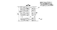
図2はPDデバイス20内の装置の構成を示す平面図である。複数の方形アパーチャ21が設けられ、規則的なアレイ内のPDフィールド内に配備され、フィールド内でアパーチャ21が近接線plに沿って配列され、各線pl内において同数のアパーチャが存在している。線plと直交する方向に沿って見たときに、アパーチャは列r1,r2,r3のシーケンスを形成しており、図示実施例において、列r1−r3は近接しておらず隔置されている。アパーチャは歪対称の規則的な配列に基づいてPDフィールドpf内に配備されており、3列目ごとのアパーチャが(n=3)で整列し、近接する列間のピッチpnがアパーチャの幅wの3倍(すなわち、pn=n×w)である。図2の構成において、近接する列間のオフセットpmはアパーチャの幅の四倍(すなわち、m=4としたときpm=m×w)である。また、線pl内で、アパーチャのオフセットはn・pm=12である。従って、フィールドpfの面積のほんの1/(n×m)=1/12のみを覆っており、同時にn×m=12画像要素のただ一つが図3に示すように露光されることが可能である。他の要素はアパーチャの画像に対して「走査方向」sdに沿って基板を移動させることによって続くステップにおいて露光される。アパーチャを制御する空間配置および回路についての詳細は米国公開特許第二003−0155534−A1を参照するものとする。
FIG. 2 is a plan view showing the configuration of the device in the
図3は基板上に生成される画像フィールドmfを示している。明瞭にする目的で、全アパーチャがこの図ではスイッチオンされていると仮定している。画像フィールドの幅wは投射システムの縮小係数によって縮小されたpfフィールドの幅Lである。画像フィールドは複数の画像素子mx(画素ともいう)からなる。基板上の画像フィールドの任意の位置に対して、アパーチャ・アレイのアパーチャ21は画像素子mxに対応しているが、アパーチャがPDフィールド域の一部を覆っているだけであり、画像素子の数の対応する部分のみが(図3においてハッチングで示す)が同時に露光される。他の画像素子も露光するために、基板がビーム下で移動され、これによって基板上で画像フィールドがシフトされる。別の方法も基板上方で画像を相対的に移動させるのに使用できることは明白である。例えば、安定基板位置でナノースケールのビームパターン処理をする一つの適切な方法において、ビームは基板上方で偏向される。図3aは可能な12(=n×m)位置を介して基板の移動する連続位置にある画素の露光を示す。画素は従ってアルファベットaからlで表わされる(ハッチングを付けて示した画素が位置aである)。全画像フィールドmfが基板41として機能するフォトレジストでカバーされたウェハの表面上方を移動され、これによって基板表面の全域を覆うことになる。走査方向sdは、ダイ・フィールドの一つのシーケンスが終了し、次のシーケンスの画像処理が開始されたときに、反転させることもできる(米国公開特許第二003−0155534−A1の図4に示すよう左から右へ、次に右から左へと交互に移動する)。
FIG. 3 shows the image field mf generated on the substrate. For the sake of clarity, it is assumed that all apertures are switched on in this figure. The width w of the image field is the width L of the pf field reduced by the projection system reduction factor. The image field is composed of a plurality of image elements mx (also referred to as pixels). For any position in the image field on the substrate, the
図4および5はPDシステム102のアーキテクチャを示す。すなわち、図4は平面図であり、図5は長手方向断面図である。図6は図5の詳細を示し、二つのアパーチャに沿った本実施例のPDシステム102を構成する一連のプレートの形態を示す。PDシステム102は積層形態で取り付けられた複数のプレート22からなり、その要素がそれぞれの機能を発揮する合成デバイスで実行される。プレート22の各々は半導体(特に、シリコン)ウェハとして実行され、その構造は当該技術において公知のマイクロ構造技術によって形成される。リトグラフ・ビームがPDフィールドpf(図5)内のアパーチャのアレイを介してプレートを横断する。各アパーチャはプレート22(図6)内で規定された一連の開口部210,220,230に対応している。
4 and 5 show the architecture of the
プレート22の各々の厚みはアパーチャの域内で約500μmから50μmである。それらの相互距離は10μmから1mm程度である。図5および6において注意しなければならないことは、長軸(アパーチャの光軸と平行なz−軸)の寸法は拡大されており、実寸でないことである。
The thickness of each of the
ビームレットのブランキングは、アパーチャに各々対応する開口部220(「ブランク開口部」)のアレイからなるブランク・プレート202として実行されたブランク手段によって制御される。各ブランク開口部220は、一連のビーム・ブランク電極221だけでなく例えばブランク・プレート202の下方表面層上に収容された電極221a,221bを制御するための回路222からなる。次に説明するようなアパーチャ規定プレートとして作用するブランク電極221は、最新技術を使用して垂直方向に生長させることによってブランク開口部の周りに形成される。クロストークおよび他の望まない作用に抗してブランク開口部をよりよいシールドを提供するために、電極221aの一つをブランク・プレート202を越える実質的な高さを有するように形成される。好ましくは、この電極221aは全装置に対して均一電位(例えば、接地電位)に接続され、一方他の電極221bには「オン」と「オフ」状態間を切り換えるための制御電圧が印加される。ブランク・プレート202のレイアウトとその回路222のさらなる詳細は、米国公開特許第二003−0155534−A1に見ることができる。
Beamlet blanking is controlled by blanking means implemented as a
PDシステム102はさらにアパーチャ・アレイ手段からなり、横方向にビームレットの形状を規定する作用をするとともに、ここではカバーとブランク・プレート201,202の後方に配置された幅w3を有する開口部のアレイを伴うアパーチャ・アレイ・プレート203(以後、短く「アパーチャ・アレイ」という)として実行される。アパーチャ・プレート203のレイアウトに関するより詳細は米国公開特許第二003−0155534−A1に見ることができる。
The
好ましくは、一連の機能プレート、カバー・プレート、ブランク・プレートおよびアパーチャ・プレートは、プレート同士間の配列、PDシステムのプレート内部およびプレート間の発熱と帯電効果が容易に制御できる方法で選択される。到来ビームの方向から見たときにカバー・プレートが頂部上に配置され、ブランク・プレートが中央に、またアパーチャ・プレートが低部に配置された図6に示す構成が、ちょうど一つの可能な構成である。他の可能性は図22に示すPDデバイス102’の構成となり、アパーチャ・プレートがカバー・プレートの機能と合成されブランク・プレート203上方に配置された「ビーム形成プレート」204になる。すなわち、ビーム形成プレートはブランク・プレート上に直接接着される。この場合において、ビームレットbmは適切な幅w3を有するアパーチャ230’を通過するように規定される。
Preferably, the series of functional plates, cover plates, blank plates and aperture plates are selected in such a way that the arrangement between the plates, the heat generation and charging effects within and between the plates of the PD system can be easily controlled. . The configuration shown in FIG. 6 with the cover plate on top, the blank plate in the center and the aperture plate at the bottom when viewed from the direction of the incoming beam is just one possible configuration. It is. Another possibility is the configuration of the
リトグラフ・ビームの方向から見てアパーチャとブランク・プレート202,203の前方において、カバー・プレート201として実行されたカバー手段が他のプレートを放射による損傷から保護するために設けられる。カバー・プレート201は照射リトグラフ・ビームlbの大半を取り上げ、粒子はブランク・プレートの通過に対応してアレイ内に形成された開口部210を通過するだけであり、開口部はブランク・フィールドbfの全面積の小さい部分のみに形成される。カバー・プレート201のレイアウトに関するより詳細は米国公開特許第二003−0155534−A1に見ることができる。
In front of the aperture and
幅w3(カバー・プレート201内の初期開口部ではなく)のアパーチャ230は、システム102から放射されるビームレットの横方向形状を規定している(図2のアパーチャの幅wに対応)。従って、厳密に言えば、用語「アパーチャ」はビームレット規定アパーチャ230によって規定されたような規定形状と幅w(図2)の開口部に対して残しておくべきであるが、一般的な用語として使用される「開口部」とは対照的に用語「アパーチャ」は図6に示すように一つのビームレットbmが伝播する一連の対応する開口部210,230,220を示すのにも使用される。
The
ブランク開口部220の幅w2は、カバー・プレート201内の開口部210の幅w1よりも大きく、これによって後者開口部によって規定されたビームレットbmは、ブランク・プレート202上の制御回路222を作動させずに前者開口部を通過させることができる。例えば、幅w2は7μm(w=5μmのアパーチャの規定幅と比較して)となる。
The width w2 of the
ブランク電極221a,221bが付勢されなければビームレットbmはパスplに沿ってプレート22の続く開口部を越えるとともに、作像システム(図1)内に作像される。これはアパーチャの「スイッチオン」状態に対応している(切替状態に関して、ブランク開口部それぞれ関連するアパーチャまたはアパーチャによって規定されたビームレット間において区別はない)。「スイッチオフ」アパーチャは横断電圧を印加して電極221a,221bを付勢することによって実行される。この状態において、ブランク電極221a,221bはビームレットbmをパスplから偏向パスp0に偏向させ、これによってビームレットは、例えばPDデバイスの後方どこかに配置されたストップ・プレート204(図1)で吸収される。
If the
ビームレットbmはかなり小さい角度だけスイッチオフ状態で偏向され、またビームレットは図6に示したようにアパーチャ230をなおも通過するが、この角度による偏向は(「スイッチオフ」)ビームレットを容易にブロックする後者位置の角度で横方向に偏向されるの充分であるにことを理解すべきである。
The beamlet bm is deflected in a switch-off state by a fairly small angle, and the beamlet still passes through the
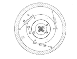
図4および5を参照して、プレート22は公知のタイプの圧電素子またはナノポジショニング素子として実現されたアクチュエータ24,25によって互いに関して位置付けされたチャック23によって保持される。垂直アクチュエータ25はスペースを保持するために設けなくてよく、次にプレート間の配置をチャック23自体の高さによって規定し、互いに単に積層することもできる。チャックの一つ、例えば図5における最後のプレートのチャックは、カップ233として形成され、これによって他のチャックの横方向位置付けが容易になっている。好ましくは、プレート22およびチャック23は同じ材料、例えばシリコンまたは動作温度範囲で同じ伸張特性を有する材料で製造される。チャックもブランク・プレート202の電気供給のために設けられ、明瞭にする目的で電線は図中には示していない。
4 and 5, the
プレート22において、開口部26が基準ビームrbを規定するために設けられている。基準ビームrbの形状は、例えばアパーチャ・プレート203内に形成された開口部内に規定され、一方他のプレート内の対応する開口部は基準ビームrbのための放射を通過させるのに充分な広さである。基準ビームrbおよびパターン化ビームpbは基板平面に向かって作像され、しかしパターン化ビームとは逆に、基準rbは基板41には到達せず、これまでに説明したようにアライメント・システム60内で測定される。チャック23は、このチャック23とこれらを保持するプレート22の相対的位置付けのためのアライメント・マーカーとして機能するアライメント開口部236をさらに有している。
グレイ・スケール
上述したPML2の概念に基づいて、基板は連続して移動され、またターゲット上の同じ画素が走査動作中一連のアパーチャによって複数回覆われる。従って、ターゲット上のある位置における一つの画素を考慮して、その画素が覆われたきに全アパーチャがスイッチオンされ、これで画素の最大露光結果となり、「ホワイト」シェードが100%に対応する。グレイ・シェード(例えば、20%)が線内のアパーチャの対応する数(例えば、線内に90のアパーチャあがるときに90の20%=18アパーチャ)をスイッチオンすることによって実行される。従って、画素の値を制御する信号がグレイ・スケール・コード、例えばnビットの2進数としてコード化された整数によって表わされる。
In the
Gray Scale Based on the PML2 concept described above, the substrate is moved continuously and the same pixel on the target is covered multiple times by a series of apertures during the scanning operation. Thus, considering a single pixel at a position on the target, all apertures are switched on when the pixel is covered, which results in the maximum exposure of the pixel, with a “white” shade corresponding to 100%. A gray shade (eg, 20%) is implemented by switching on the corresponding number of apertures in the line (eg, 20% of 90 = 18 apertures when 90 apertures are in the line). Thus, the signal that controls the value of the pixel is represented by a gray scale code, for example, an integer encoded as an n-bit binary number.
グレイ・レベルを実現するために、米国公開特許第二003−0155534−A1は線内のアパーチャの全数をカラムに、所望のグレイ・レベルの数に対応するカラム数(例えば、30グレイ・レベルに対して30カラム)に副分割することを提案している。電子機器においてに対する大きいスペース必要条件のためにシフト・レジスタをアパーチャの密集したアレイ間に配置しなければならないという厳しい問題がある。この問題に対する解決策として、走査速度に対する係数nを掛けた速度で連続してnビットデータに供給し、グレイ・コンパレータに供給して30グレイ・レベル・カラムの各々内に1ビット丁度にする。1ビットシフト・レジスタが、「ブラック・アンド・ホワイト」データ流れを各カラム内の一つのアパーチャ・サイトから次のアパーチャにトグルしている間、次のグレイ・カラムのために利用可能なnビット・データを維持し、カラム間の相互接続がデータ流れをグレイ・カラムの出発点(すなわち、アパーチャ列のオフセットによって提供されたスペースで)に配置されたメモリ・バッファに転送する。ここでデータが、時間遅延(すなわち、前回のグレイ・カラムを通るデータ流れの全トグル時間)がバランスするまで、バッファされる。 To achieve gray levels, U.S. Patent Publication No. 003-0155534-A1 uses the total number of apertures in a line as columns and the number of columns corresponding to the desired number of gray levels (eg, 30 gray levels). On the other hand, it is proposed to subdivide into 30 columns). Due to the large space requirements for electronics, there is a severe problem that shift registers must be placed between dense arrays of apertures. As a solution to this problem, n-bit data is continuously fed at a rate multiplied by a factor n to the scan rate and fed to a gray comparator to make exactly one bit in each of the 30 gray level columns. N bits available for the next gray column while the 1-bit shift register toggles the “black and white” data stream from one aperture site in each column to the next aperture Maintain data and interconnect between columns transfer the data stream to a memory buffer located at the starting point of the gray column (ie, in the space provided by the aperture column offset). Here the data is buffered until the time delay (ie, the total toggle time of the data flow through the previous gray column) is balanced.
本発明はPDデバイスを使用して走査基板上に画像をエンコードし転送するより効果的な方法でPML2の概念を改善することを目的としている。本発明によれば、ブランク・プレート内のブランク開口部およびブランク開口部(および対応するアパーチャ)のスイッチ状態を制御する偏向手段の制御は、個々のブランク開口部間における遅延時間の処理を考慮せずに、1ビット信号を直接ブランク・プレートに供給することを許容する方法で組織化することは、グレイ・スケール信号に関するさらなる処理を必要とせず、特にこの目的のためにデバイスを増大または低減する必要はない。 The present invention aims to improve the PML2 concept in a more effective way to encode and transfer images onto a scanning substrate using a PD device. According to the present invention, the control of the deflection means for controlling the switch states of the blank openings and the blank openings (and corresponding apertures) in the blank plate allows for the processing of delay times between the individual blank openings. Without organizing in a way that allows a 1-bit signal to be fed directly to the blank plate, no further processing on the gray scale signal is required, especially increasing or decreasing the device for this purpose There is no need.
ブランク・プレートおよびグレイ・グループ
以下、本発明をアパーチャの構成がn=6とm=6(n×m=36)の概念で説明する。ウェハに対して説明されるべき最小構成サイズは45nm(45nmの分解線とスペースを伴う45nmノードとする)であり、最小スポットは25nm(図3において画素幅×、一つのアパーチャの幾何学的画像に等しい)である。画像フィールド幅fwは81μmである。200×縮小投射システム(上記説明参照)に関するこの画像フィールドを製造するために、正方形PDフィールドが幅L=16.2mmを有し、線の数pl=L/W=3240に対応し、また3240ビット・ストリームが到来データ・ストリームによってアドレスされることになる。横断方向において、列r1−r3の各々にfw/(n・x)=L/(n・w)=90アパーチャがある。
Blank Plate and Gray Group Hereinafter, the present invention will be described based on the concept that the aperture configuration is n = 6 and m = 6 (n × m = 36). The minimum feature size to be accounted for for the wafer is 45 nm (assuming a 45 nm node with a 45 nm resolution line and space) and a minimum spot is 25 nm (pixel width in FIG. 3, geometric image of one aperture). Equals). The image field width fw is 81 μm. To produce this image field for a 200 × reduced projection system (see description above), the square PD field has a width L = 16.2 mm, corresponds to the number of lines pl = L / W = 3240, and 3240 The bit stream will be addressed by the incoming data stream. In the transverse direction, each row r1-r3 has fw / (n · x) = L / (n · w) = 90 apertures.
本発明は次の考えに基づいている。グレイ値は例えば0から31の範囲にある値の数によって表わされる。与えられた範囲において、一連の数が範囲の全値(または範囲が完全に示す必要がなければ少なくとも全ての適切な値が、一連の数から選択され複数の和として表わすことができる。例えば、一連の数(1,2,4,8,16)が0から31の全ての値を表わすように選択される。これは2の累乗分解であり、一連の数から数の選択は常に一つである。他の一連の数も同様に適しており、ある数が一回を超えて現われてもよいことに注意しなければならない。例えば、一連の数(2,2,3,6,14)は、値1,12,14,26を除いた0から27の範囲を表わすのに使用することもできる。この一連の数において、値18は2+2+14=1・2+1・2+0・3+0・6+1・14またはショートハンド(11001)で表わすことができる。このショートハンドは一連のビットであり、各々一連の一つの数を表わし、関連する数が和であれば値1で、そうでなければ0をとる。
The present invention is based on the following idea. The gray value is represented by the number of values in the range of 0 to 31, for example. In a given range, a series of numbers is the total value of the range (or at least all suitable values are selected from the series of numbers if the range does not have to be fully shown, and can be expressed as a sum of a plurality. A series of numbers (1, 2, 4, 8, 16) is selected to represent all values from 0 to 31. This is a power of 2 decomposition, and the choice of numbers from a series of numbers is always one. It should be noted that other series of numbers are equally suitable, and some numbers may appear more than once, for example, a series of numbers (2, 2, 3, 6, 14 ) Can also be used to represent a range from 0 to 27, excluding the
総計が任意の強度になるまで加算された露光の明瞭な数を発生するために、グレイ数を表わす数のこのような分解を(直線増大または縮小を使用する代わりに)一連のビットに使用してアパーチャがスイッチオンまたはスイッチオフされるように決定することができる。この一連のビットはグレイ信号として使用され、また各ビットはブランク開口部の一つのグループ(「グレイ・グループ」)に関連している。各グレイ・グループ内の開口部の数は、グレイ・ビットを表わす数によって特定付けられる。 In order to generate a clear number of exposures added until the total is of arbitrary intensity, such a decomposition of the number representing the gray number is used for a series of bits (instead of using linear increase or decrease). The aperture can be determined to be switched on or off. This series of bits is used as a gray signal, and each bit is associated with one group of blank openings (a “gray group”). The number of openings in each gray group is specified by a number representing a gray bit.
N・2Mブランク開口部からなる線を伴う例として、Mグループを使用する実行に対応して2の乗数分解がグレイ・レベルのために使用され、各々N・2nアパーチャからなり、n=0からM−1がグレイ・ビットの指数に対応し、またNが最低(ゼロではない)グレイ・レベルのアパーチャの数である。従って、0から2M−1のMビット範囲によってスパンされたいずれのグレイ・レベルも簡単な2進数によって表わすことができ、各グレイ・レベルxがx・Nブランク開口部の数に対応している。(等価的に、開口部の仕切りは(N,2N,...,2M−1N)である。)例えば、「0」と「31」間の値を生成するために、5ビットに対応する直線独立基準が使用される。この例において、(デシマル)数13が2進数(01101)で表わされるので、グレイ・レベル13は数13=1+4+8の仕切りに基づいて発生され、このような方法において指数0,2および3を伴うグループがアクティブであり、Nをとると、22・N=4・Nおよび23・N=8・Nのブランク開口部がそれぞれ累積露光線量を受け、一方残りのグループはアクティブではなく、また全く寄与しない。複数のレベル(例えば、2Mのグレイ・レベル)を構成数(例えば、1から2M−1のM2進乗数に)仕切ることによるこのアプローチの特定する利点は、データ転送の問題がずっと簡単になることである。非2進乗数分解が使用された場合、同じ考えが適用される。
As an example with a line consisting of N · 2 M blank openings, a multiplier decomposition of 2 is used for gray levels corresponding to the implementation using M groups, each consisting of N · 2 n apertures, n = 0 to M-1 corresponds to the exponent of gray bits, and N is the number of apertures with the lowest (non-zero) gray level. Thus, any gray level spanned by an M bit range from 0 to 2 M −1 can be represented by a simple binary number, with each gray level x corresponding to the number of x · N blank openings. Yes. (Equivalently, the partition of the opening is (N, 2N,..., 2 M−1 N).) For example, to generate a value between “0” and “31”, 5 bits The corresponding straight line independent criterion is used. In this example, since the (decimal)
ブランク開口部の各グレイ・グループのために、シフト・レジスタの第一要素のみが、すなわち、グループ当り一つが到来データ流れ(または逆方向に走査するための最後の要素、走査方向を逆にするために必要な電極の詳細は米国公開特許第二003−0155534−A1に開示されている)によってリフレッシュされる。グレイ・グループに供給され、またその第一ブランク開口部のための制御信号として直接使用される信号は、以下グループ制御信号と呼ぶ。グループ制御信号はターゲットを越えてパターン画像の走査動作と一致することが必要なときに遅延を提供する遅延手段を介して一つのブランク開口部から次の開口部に渡される。単一ビット・グレイ制御信号(一線当り1クロック・サイクル当り1ビット)が、グレイ・グループのために全てそれぞれの露光を発生するのに充分である。この概念に従って、ブランク・フィールドbfへ供給されるべき供給線の数が、ある先行技術、特に全てのアパーチャが外部から個々にアドレスされるヤスダ他の特許と比較して大きく低減される。さらにアパーチャ・プレートの上方または下方サイドからデータ流れに供給されるスペースが充分になる。 For each gray group of blank openings, only the first element of the shift register, ie one per group, is the incoming data stream (or the last element to scan in the reverse direction, reverse the scan direction) The details of the electrodes necessary for this are refreshed by U.S. Pat. No. 2,003-0155534-A1). The signal supplied to the gray group and used directly as a control signal for its first blank opening is hereinafter referred to as a group control signal. The group control signal is passed from one blank opening to the next through delay means that provides a delay when it is necessary to match the pattern image scanning operation across the target. A single bit gray control signal (one bit per clock cycle per line) is sufficient to generate all the respective exposures for the gray group. In accordance with this concept, the number of supply lines to be supplied to the blank field bf is greatly reduced compared to certain prior art, especially Yasuda et al. Patents in which all apertures are individually addressed from the outside. Furthermore, there is enough space to be supplied to the data stream from the upper or lower side of the aperture plate.
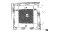
本発明に基づくブランク・プレート702の一つの適切な実施例を図7の平面図に示す(カバーおよびアパーチャ・プレートのようなPDデバイスの他のプレートはこの図を明瞭にするために取り外さなければならない)。ブランク・プレート702の中央において、ブランク開口部は図2で上述したようにPDフィールドを形成する折れ線の正規アレイ内に配備されている。結果として、ブランク・フィールドbf内に各々90のブランク開口部を伴うブランク開口部の3240の線がある。この開口部の構成はスケールで表わすことができないので、フィールドbfを図7においてクロスハッチングのみで表わしている。ブランク・プレート702の周縁において、生成されるべきデータ流れが複数のパッド接続部713を介して供給される。パッド接続部の必要サイズのために、その数は制限され、パターン信号がパッド接続部の数に対応するデータ幅でより高いデータ率でより小さいデータ幅に多重送信される。フィールドbfを取り囲んでより好ましく配置されたコンバータ手段721,722,723,724が、データを制御信号にデコードし、これがフィールドbf内のブランク開口部に印加される。これらの信号は複数の供給線711(供給線のほんの一部を明瞭にする目的で示しており、実際には供給線711の数は次に説明するように数千本である)を使用して供給される。
One suitable embodiment of a blank plate 702 according to the present invention is shown in the plan view of FIG. 7 (other plates of the PD device such as the cover and aperture plate must be removed for clarity of this view). Must not). In the middle of the blank plate 702, the blank openings are arranged in a regular array of polygonal lines forming a PD field as described above in FIG. As a result, there are 3240 lines of blank openings with 90 blank openings each in the blank field bf. Since the configuration of the opening cannot be represented by a scale, the field bf is represented by only cross hatching in FIG. At the periphery of the blank plate 702, the data stream to be generated is supplied via a plurality of
図8を参照して、各線のブランク開口部は次に説明するようにグレイ・グループに組織化される。各グループの開口部は連続して配置され(図9aも参照)、さらにグループ化はブロック・プレート702の全線に対して同じである。結果として、線の対応するグループは線に対して垂直に(または、等価的に走査方向と直交して)走行するストライプを形成する。これらのストライプによって覆われた域は参照の目的で図8で破線で輪郭が描かれて、また基準シンボルa1からa6によって示されている。この実施例において、グループは次のブロック開口部の数、すなわち、図8の左から右へ8,16,32,28,2,4を有している。このようなアパーチャの分布は0から45のレベル(レベル当り2アパーチャ)、すなわち46グレイ・レベルを発生するように許容される。同じグレイ・スケール値がグループ信号をそのように再配列し、グループ制御信号のために適切な位相シフトを適用するだけで実行することができるように、同じ構成が多くの順序で、例えばグループのサイクル的並べ替えで行なわれることに注意しなけれならない。
Referring to FIG. 8, the blank openings for each line are organized into gray groups as described next. The openings in each group are arranged sequentially (see also FIG. 9a), and the grouping is the same for all lines of the block plate 702. As a result, corresponding groups of lines form stripes that run perpendicular to the lines (or equivalently orthogonal to the scanning direction). The areas covered by these stripes are outlined with dashed lines in FIG. 8 for reference purposes and are also indicated by reference symbols a1 to a6. In this embodiment, the group has the next number of block openings,
図9はグループの配列の詳細を示す。より明瞭にするために(また図を簡略にするために)、ブランク開口部の配列は図9から13、15から17および図21においてn×m=4×3=12として示している。次の実施例では実際にn×m=36を使用しているが、次の考えを容易に取り入れることができ、またこれらのケース間で適用できることを覚えておかなければならない。 FIG. 9 shows the details of the group arrangement. For more clarity (and to simplify the figure), the arrangement of blank openings is shown as n × m = 4 × 3 = 12 in FIGS. 9 to 13, 15 to 17 and FIG. Although the following example actually uses n × m = 36, it should be remembered that the following idea can be easily incorporated and applied between these cases.
図9aはブランク・フィールドの第一線の端(図8の最も左のアパーチャ)を示す。最後の四つのブランク開口部910は最後のグループg6を形成し、これらの前二つのブランク開口部910は二番目の最終グループg5である。各グループに対して、第一ブランク開口部が供給線911(図8の線gfの一つに対応)を介してそれぞれのグループのブランク信号が供給される。供給線は普通ウェハの金属層および(または)信号と同期する電子機器上に形成されたスクリーン状導電線からなる。もしよければ、シフト・レジスタを介するトグル操作で信号をグレイ・グループに供給するのに使用することもできる。
FIG. 9a shows the end of the first line of the blank field (the leftmost aperture in FIG. 8). The last four
図9bは一連のグループが線に対して同じであるとき、ストライプa4,a5,a6からの近接線のグループg4,g5,g6の概要がどのようになっているかを示す。(図9bは破線ボックスD9で示した図8の詳細である)。各グループ内で、信号は遅延手段921と相互接続線914からなる相互接続部によって一つの開口部から次の開口部へ伝播される。遅延手段921は、パターンがPDフィールド(米国公開特許第二003−0155534−A1、図17および18と比較して)線内の連続アパーチャ間で適切な時間遅延を提供するように作用する。図9の特定例において、遅延手段921は一連のシフト・レジスタとして実現され、また各遅延手段は接続された二つの開口部間の傾斜域を使用する。
FIG. 9b shows how the group of adjacent lines g4, g5, g6 from stripes a4, a5, a6 is outlined when the series of groups are the same for the lines. (FIG. 9b is a detail of FIG. 8 indicated by the dashed box D9). Within each group, signals are propagated from one opening to the next by an interconnect consisting of delay means 921 and
マルチプレクサから各グループの第一アパーチャへのグループ制御信号の走行時間のために、例えば適切な信号位相を設定することによって事前処理中に可能な遅延が補正されれば、必要とされる信号同期化を達成するための付加的なメモリ・バッファは既に説明した遅延手段の他に何も必要ではない。付加的な高周波電子技術の迂回は従来技術のBAAレイアウトと比較して相当簡略化できる。図7のレイアウトにおいて、グループ・ブランク信号が図8に示したように全サイドから供給される。ブランク・プレート702のロジック、および特にブランク開口フィールドbfにおいて、米国公開特許第二003−0155534−A1において必須であるグレイ・コンパレータもDRAMバッファも必要ではない。コンバータ721−724のようななおも必要とされる高周波論理電子機器は、フィールドbf外部の厚いウェハ域内に形成することができる。説明したチップ・レイアウトは、複数の供給線gfに接続された熱およびタイミングの問題を軽減する。 If the delay possible during pre-processing is corrected for the transit time of the group control signal from the multiplexer to the first aperture of each group, for example by setting the appropriate signal phase, the required signal synchronization No additional memory buffer is required to achieve this in addition to the delay means already described. The bypass of additional high frequency electronic technology can be considerably simplified compared to the prior art BAA layout. In the layout of FIG. 7, group blank signals are supplied from all sides as shown in FIG. In the logic of the blank plate 702, and particularly in the blank aperture field bf, neither the gray comparator nor the DRAM buffer, which is essential in US Published Patent Application No. 003-0155534-A1, is required. Still required high frequency logic electronics such as converters 721-724 can be formed in a thick wafer area outside the field bf. The described chip layout alleviates thermal and timing issues connected to multiple supply lines gf.
従来技術に対する本発明の主たる違いの一つは、グループ・ブランク信号がブランク開口部の対応するグループの第一ブランク開口部に(より正確には、その開口部のそれぞれの制御回路に)直接配信されることである。この状態は代表する数の供給線gfにつき図8に示し、各々コンバータ721−724の一つから始まり、ストライプa1−a6内のグループの一つ第一ブランク開口部のサイトで終わっている。実際に存在する(すなわち、3240×6=19,440本)の非常に複数の供給線のために全てこれらの線gfを図8に示してない。むしろ図8に示した線gfは線のパスの全体のアイデアを表わしている。供給線gfは交差しないことを認識することが重要で、この条件が好ましく、線のパスはフィールドbfの最も近いサイドに直接走行するように選択される。コンバータ721−724が配置された周りのレファレンス・マーク26の位置も図8に示す。
One of the main differences of the present invention over the prior art is that the group blank signal is delivered directly to the first blank opening of the corresponding group of blank openings (more precisely to the respective control circuit of that opening). It is to be done. This state is shown in FIG. 8 for a representative number of supply lines gf, each starting from one of the converters 721-724 and ending at the site of one first blank opening in the group in stripe a1-a6. All these lines gf are not shown in FIG. 8 because of the very large number of supply lines actually present (ie 3240 × 6 = 19,440 lines). Rather, the line gf shown in FIG. 8 represents the overall idea of the line path. It is important to recognize that the supply lines gf do not intersect and this condition is preferred and the path of the line is chosen to run directly to the nearest side of the field bf. The position of the
この構成の結果、アパーチャ間に付加的なスペース(米国公開特許第二003−0155534−A1の「列オフセット」のような)を必要とするメモリ・ブロックもグレイ・コンパレータも必要としない。 As a result of this configuration, there is no need for memory blocks or gray comparators that require additional space between apertures (such as the “column offset” of US Patent Publication No. 003-0155534-A1).
図10から12はブランク・プレート内のグループ制御信号の経路を示す。図10は図8(破線ボックスD10によってマークされた)の詳細を示し、ストライプa4の外側領域のブランク開口部910に供給される供給線gfを示している。これらのグループ制御信号はフィールドbfの底サイド(図8と10に関して底サイド;走査方向に関して横方向サイド)から接続フィールド912で供給される。各ブランク開口部に対して、図10から12においてボックス922(図12および12においてハッチングされた)エリアが確保され、各ブランク開口部910の遅延手段の回路が偏向素子の関連する電気制御素子(コンデンサ)の他に設けられる。従って、ボックス922は図9の部材921に対応するが、ブランク開口部のアレイに対してスペースの異なる割り当てをする。繰り返しカウントn=4のために、供給線gfは4線のグループ内に同様にグループ分けされる。
10 to 12 show the path of the group control signal in the blank plate. FIG. 10 shows details of FIG. 8 (marked by the dashed box D10) and shows the supply line gf supplied to the
図11はそれぞれのグループ内でグループ制御信号の伝播を提供する連続ブランク開口部間の相互接続を示す。各相互接続線914はブランク開口部に属する一つのボックス922にある遅延手段の出力で始まり、次のブランク開口部の入力に走行し、ここで関連する遅延手段の入力と偏向電極の制御部に供給される。相互接続線914は、図10に示した供給線のような異なる電気層内に形成されている。
FIG. 11 shows the interconnections between successive blank openings that provide group control signal propagation within each group. Each
図12はグループの端にある相互接続線を示す。グループの最終ブランク・アパーチャに信号を供給する相互接続線914’は、遅延手段がこのブランク開口部に必要としないので、偏向電極制御部に直接供給されている。グレイ・グループの最終ブランク開口部が、グループを介するデータ伝播のためのデッドエンドを表わしている。線の端で信号の反射を回避することを保証するために、データ線は端末抵抗器(図示せず)のような適切な電気手段によって終端されなければならない。データ線の終端はPDフィールドの外部で実行してブランク・フィールドbf内に発生する熱の低減を許容する。線を閉止するための他の可能性は、各信号のための第二線(帰還線)となるか、または「ツイスト・ペア」のような高周波技術となる。これらの観点とは別にして、図12は11に対応する。 FIG. 12 shows the interconnect lines at the end of the group. The interconnect line 914 'that feeds the signal to the final blank aperture of the group is fed directly to the deflection electrode control, since no delay means are required at this blank opening. The final blank opening of the gray group represents the dead end for data propagation through the group. In order to ensure that signal reflection at the end of the line is avoided, the data line must be terminated by appropriate electrical means such as a terminal resistor (not shown). The termination of the data line is performed outside the PD field to allow the heat generated in the blank field bf to be reduced. Another possibility for closing the line is the second line (feedback line) for each signal, or a high frequency technique such as a "twisted pair". Apart from these points of view, FIG.
上述の実施例において、ブランク開口部のグループは各線において同じ順序に従っている。しかし、シーケンスは線間で変更できる。このような変形例を図13に示す。 In the example described above, the groups of blank openings follow the same order in each line. However, the sequence can be changed between lines. Such a modification is shown in FIG.
図13は図9と類似したフィールドbfのエッジを示す。しかし、この変形例において、一連のグループは各線で異なる。各線において開口部の数はなおも仕切り(2,4,8,16,28,32)に従っているが、実際の順序はこれら数の種々の並べ替えを表わしている。より詳しく説明すると、図13に詳細に示した一つの可能なパターンは、図13に示したような最も上の線から始まる順序であるグレイ・グループの次のシーケンス、すなわち、(16,28,8,32,2,4),(4,16,28,8,32,2),(2,4,16,28,8,32),(32,2,4,16,28,8),(8,32,2,4,16,28),(28,8,32,2,4,16)となり、次に始まりからの繰り返しとなる。このシーケンスはグループのサイクル変換を実現し、他の実施例においてこのシーケンスの反転または自由な並べ替えを使用することができる。 FIG. 13 shows the edges of field bf similar to FIG. However, in this variation, the series of groups is different for each line. Although the number of openings in each line still follows the dividers (2, 4, 8, 16, 28, 32), the actual order represents various permutations of these numbers. More specifically, one possible pattern shown in detail in FIG. 13 is the next sequence of gray groups in order starting from the top line as shown in FIG. 8, 32, 2, 4), (4, 16, 28, 8, 32, 2), (2, 4, 16, 28, 8, 32), (32, 2, 4, 16, 28, 8) , (8, 32, 2, 4, 16, 28), (28, 8, 32, 2, 4, 16), and then repeat from the beginning. This sequence implements a group cycle conversion, and in other embodiments, this sequence inversion or free permutation can be used.
PDデバイス内でグレイ・グループの並べ替えシーケンスを使用する主たる利点は、ビーム直径の断面上で動的構成ビームの電流密度分布を効果的に滑らかにすることである。従って、電流密度分布が特定レイアウトで全く無関係となり、クーロン相互作用によるパターン関連画像歪を回避する。パターン関連画像歪はPML2内の使用可能電流の主たる制限要素の一つであり、生産性と全体の性能を低下させる。 The main advantage of using a gray group permutation sequence in a PD device is to effectively smooth the current density distribution of the dynamically configured beam over the beam diameter cross-section. Therefore, the current density distribution becomes completely irrelevant in the specific layout, and pattern-related image distortion due to Coulomb interaction is avoided. Pattern-related image distortion is one of the main limiting factors of the usable current in PML2 and reduces productivity and overall performance.
データ事前処理
図14はブランク・プレートのためのデータ事前処理およびデータ・ローディングを示す。既に説明したように、ブランク・プレートへ供給される並列データ(3240線掛ける6グレイ・グループ)の安定流れがある。ブランク・プレートに対して利用可能な線の制限数(例えば、200未満のパッド接続部713)だけがあるという事実のために、マルチプレキシング工程がこのボトルネックの周りで操作するのに使用される。換言すれば、任意の定格(例えば、8MHz)で複数の並列データ(6×3240ビット)が高いデータ定格(144×8=1152MHz)の少数データ(例えば、135ビット)に変換される。ブランク・プレート上で、データがコンバータ721−724内で並列データに変換し直され、供給線gfを介してグレイ・グループに印加することができる。ブランク・プレートでデータ定格を下げるために、供給線がPDフィールドの全周縁の周りに配備される。例えば、上述したように25mmチップ上に生成された16.2mm幅の方形PDフィールドで、80μm幅を有する少なくとも1250までの接着パッドが矩形フレームに沿って線に嵌め込むことができ、16ビット・マルチプレキシング工程によって128MHzまでデータ定格の低減が許容される。
Data Preprocessing FIG. 14 shows data preprocessing and data loading for a blank plate. As already explained, there is a stable flow of parallel data (3240 lines by 6 gray groups) fed to the blank plate. Due to the fact that there is only a limited number of lines available for the blank plate (eg less than 200 pad connections 713), a multiplexing process is used to operate around this bottleneck. . In other words, a plurality of parallel data (6 × 3240 bits) at an arbitrary rating (for example, 8 MHz) is converted into a small number of data (for example, 135 bits) having a high data rating (144 × 8 = 11152 MHz). On the blank plate, the data can be converted back to parallel data in converters 721-724 and applied to the gray group via supply line gf. In order to reduce the data rating on the blank plate, supply lines are deployed around the entire periphery of the PD field. For example, in a 16.2 mm wide square PD field generated on a 25 mm chip as described above, up to 1250 bond pads having a width of 80 μm can be fitted into a line along a rectangular frame, The multiplexing process allows a data rating reduction to 128 MHz.
データ準備工程は、大量記憶装置に保持されたターゲット・パターンから始まり、また最新技術方法に基づいて、粒子−光学投射システム(図1)のような全ての必要な修正を考慮してグレイ・スケール・パターンに変換される。このグレイ・スケール・パターンは既に画素化フォームに規定されている。このファイルのグレイ・スケール・データは、ブランク・フィールドbf内のグレイ・グループに基づいてグレイ値の分解によってグレイ・ビット・データに変換される。こうして得られたグレイ・データ・ビットは個々の位相シフトに基づいて互いにシフトされる。グレイ・グループはブランク・フィールドbf上にあるそれぞれ第一ブランク開口部の相対位置のために必要である。このデータ処理ステップはパターン書き取り処理を制御するのに直接使用することができる位相シフト・グレイ・ビット・データ流れを発生する。しかし、好ましくはオフライン・データ準備がなされ、ストリーム・データが中間記憶装置に都合よく記憶される。この中間記憶操作のために、ビット・データを圧縮してデータ・ファイルへのコンパクト記憶を許容する中間データ形態にすることが有利である。設定されるべき位相シフトがクロック・サイクルの整数値でなければ、信号はグレイ画素データの補間によって計算しなければならない。好ましい実施例によれば、ブランク・プレート上のアパーチャの位置およびアパーチャへの信号転送回数は、位相シフトがクロック・サイクルの整数となる方法で選択され、次に位相シフトが付加的なデータ処理なしにグレイ・データ流れの順方向または逆方向へのシフトによって容易に調整される。ターゲットの実際露光の時間に、中間データ・ファイルがデコードされ、位相シフトされたグレイ・ビット・データ流れを回復する。この流れは低いハンド幅と高いデータ定格(上述したようなマルチプレキシング)のデータ・フォーマットにエンコードされる。またこの形態において、ブランク・プレートに伝送される。ブランク・プレート上で、データ流れがコンバータ手段721−724内にデコードされるとともにブランク・フィールドbfに供給される。 The data preparation process begins with a target pattern held in mass storage and, based on state-of-the-art methods, takes into account all necessary modifications such as a particle-optical projection system (FIG. 1) in gray scale. • Converted to a pattern. This gray scale pattern is already defined in the pixelated form. The gray scale data of this file is converted to gray bit data by a gray value decomposition based on the gray groups in the blank field bf. The resulting gray data bits are shifted relative to each other based on the individual phase shifts. Gray groups are necessary for the relative position of each first blank opening on the blank field bf. This data processing step generates a phase shifted gray bit data stream that can be used directly to control the pattern writing process. However, preferably offline data preparation is made and stream data is conveniently stored in the intermediate storage. For this intermediate storage operation, it is advantageous to compress the bit data into an intermediate data form that allows compact storage into a data file. If the phase shift to be set is not an integer number of clock cycles, the signal must be calculated by interpolation of gray pixel data. According to a preferred embodiment, the position of the aperture on the blank plate and the number of signal transfers to the aperture are selected in such a way that the phase shift is an integer number of clock cycles, and then the phase shift is without additional data processing. Easily adjusted by shifting the gray data stream forward or backward. At the time of the actual exposure of the target, the intermediate data file is decoded to recover the phase shifted gray bit data stream. This stream is encoded into a data format with a low hand width and a high data rating (multiplexing as described above). In this form, it is transmitted to the blank plate. On the blank plate, the data stream is decoded into the converter means 721-724 and fed to the blank field bf.
このデータ事前処理経路を使用することにより、データのバッファ処理はブランク・プレートまたはPDデバイス上で必要ではない。データ流れのグレイ・ビット(グループ制御信号)への分解とその同期化は長いCPU時間を必要とし、この処理は、露光前にオフラインで実行されるのが好ましい。 By using this data pre-processing path, data buffering is not required on blank plates or PD devices. The decomposition of the data stream into gray bits (group control signals) and their synchronization require a long CPU time and this process is preferably performed off-line before exposure.
本発明は先行技術に対して幅広い利点を提供する。 The present invention offers a wide range of advantages over the prior art.
−ブランク・プレートの複雑さが大きく低減されている。複雑な配線だけでなく高価なメモリ・ブロックまたはバッファもグレイ・スケール・データの処理のために必要としない。 -The complexity of the blank plate is greatly reduced. Not only complicated wiring but also expensive memory blocks or buffers are not required for processing gray scale data.
−緩和されたリスク。ブランク・プレートのボード上の回路が低減されているので、発熱が大きく低減される。同じ理由で、製造リスクが軽減され、またX線照射に対する抵抗が改善される。ダウンスケーリングが、シフト・レジスタ電子機器とリトグラフ・ノード両方に関して促進される。付加的に、欠陥のリスクが欠陥修正概念によって低減される。 -Mitigated risk. Since the circuitry on the blank plate board is reduced, heat generation is greatly reduced. For the same reason, manufacturing risk is reduced and resistance to X-ray irradiation is improved. Downscaling is facilitated for both shift register electronics and lithographic nodes. In addition, the risk of defects is reduced by the defect correction concept.
−大々的な性能の改善。これらはグレイ・レベルの増大数、アパーチャの増大密度(増大空隙率)、空間電荷をよりよく制御することを許容するユニークでないコーディングおよびパターン依存歪を使用する可能性による。 -Major performance improvements. These depend on the increased number of gray levels, the increased density of apertures (increased porosity), the possibility of using non-unique coding and pattern-dependent distortion that allows better control of space charge.
−有利なデータ事前処理。簡単な「オフライン」ルーチンが全体的低減転送定格で伝送することができる時間遅延信号を生成できる。 -Advantageous data pre-processing. A simple “offline” routine can generate a time delay signal that can be transmitted with an overall reduced transfer rating.
エキストラ・グレイ・グループ;欠陥修正
グレイ・スケーリングに関連する可能な欠陥と他の問題を考慮するために、1線当りの欠陥数に依存して可能にされたり、不可能にされたりできるスペア・ブランク開口部を含めることが可能である。このオプションを提供するために、必要とする以上のアパーチャがあるチャネルまたは全チャネルのために構成するこができ、あるいはより有効であると思われれば、付加的な「エキストラ・アパーチャ」グループが各線に付加でき、これによって必要とするときに、例えば対応する接続線の合焦イオン・ビーム修正によって物理的に必要なとき、または設置ロジックを使用するソフトウェア制御スイッチングによって1線当りのアパーチャの特定数を「稼動」することができる。
Extra Gray Group; Defect Correction Spares that can be enabled or disabled depending on the number of defects per line to account for possible defects and other problems associated with gray scaling A blank opening can be included. To provide this option, an additional “extra aperture” group can be configured for each channel that has more apertures than needed, or can be configured for all channels, or if deemed more effective. A specific number of apertures per line when needed, for example physically required by focused ion beam modification of the corresponding connecting line, or by software controlled switching using installation logic Can be “run”.
欠陥修正のための可能なプロシージャは、1)テスト・パターンおよびビーム分析機器を使用して校正によって1線当りのエキストラ・アパーチャの必要数を決定する。2)個々のグループ制御信号によってアドレスすることのできるエキストラ・アパーチャの必要数を稼動するようにブランク・プレートのソフトウェア制御スイッチングまたは修正。3)各線の最終ビットの最高達成可能修正をデータ事前処理する。 Possible procedures for defect correction are: 1) Determine the required number of extra apertures per line by calibration using test patterns and beam analysis equipment. 2) Software control switching or modification of the blank plate to run the required number of extra apertures that can be addressed by individual group control signals. 3) Preprocess the highest achievable modification of the last bit of each line.
例えば、図8の実施例において、46のグレイ・レベルで、仕切り(8,16,32,28,2,4)の代わりに線内において、最初のグレイ・グループ内に一つの欠陥があり、また三番目のグレイ・グループ(アンダーラインを付した番号によって示す)内に二つの欠陥がるために、(7,16,30,28,2,4)のみが利用可能であり、適切な修正が五つのグレイ・グループと一つのエキストラ・グループのグレイ・レベルに対して事前計算されれば、少なくとも三つのブランク開口部(「アパーチャ」)を有するエキストラ・グループが少ないレベルのためのみに発生する1レベル(1アパーチに対応)1/2の最大エラー線量として0と45(1レベル当り2アパーチャ)の全値を近似するのに充分である。図15は五つのブランク開口部970を有するエキストラ・グループg7を伴う線の端部を示している。これらブランク開口部の最後の二つは不作動にされ、これによって三つの稼動ブランク開口部が残される。グループg7は他のグループのように供給線971によって制御される(図9aと比較)。ブランク開口部を容易に不作動にする方法を提供するために、連続アパーチャ間の接続部974のセグメント973が表面上に実行される。例えばレーザまたはレーザビームによる構造上の修正ステップにおいて、このセグメントは非導電性とし、最終から2番目のセグメント973’に対して図15に示したような接続部で効果的に遮断して、このセグメント後方の全ブランク開口部を不作動にすることができる。
For example, in the embodiment of FIG. 8, at the gray level of 46, there is one defect in the first gray group in the line instead of the divider (8, 16, 32, 28, 2, 4), Also, because there are two defects in the third gray group (indicated by the underlined number), only ( 7 , 16, 30 , 28, 2, 4) is available and appropriate corrections If pre-computed for the gray levels of five gray groups and one extra group, only occurs because there are few extra groups with at least three blank openings ("apertures") It is sufficient to approximate all values of 0 and 45 (2 apertures per level) as a maximum error dose of 1 level (corresponding to 1 aperture) ½. FIG. 15 shows the end of a line with an extra group g7 having five
図13の構成に関する一つのさらなる例において、線は各線(図示せず)内のある適切な位置で付加されたエキストラ・グループ内に5個のブランク開口部によって延長されている。グレイ・グループは(16,28,8,32,2,4;0),(3,16,26,8,32,2;3),(2,4,16,28,8,32;0), (32,1,3,16,27,6;5),(8,32,2,4,16,28;0),(28,8,32,2,4,16;0)となり、第二および第四線3および5のアパーチャがそれぞれ故障すれば(故障ブランク開口部を伴うグループを表わす数にアンダーラインを付す)、そのそれぞれの線内にある実際の位置にかかわらずエキストラ・グループが常に終端で書き取りされる。
In one further example relating to the configuration of FIG. 13, the lines are extended by five blank openings in an extra group added at some appropriate location within each line (not shown). The gray group is (16, 28 , 8, 32, 2, 4; 0), ( 3 , 16, 26 , 8, 32, 2; 3), (2, 4, 16, 28 , 8, 32; 0 ), (32, 1 , 3 , 16, 27 , 6 ; 5), (8, 32, 2 , 4 , 16, 28; 0), (28, 8 , 32, 2 , 4 , 16; 0) If the apertures in the second and
図16は故障修正のためのエキストラ・ブランク開口部を含める別の方法を示す。グループge5,ge6の終端において、エキストラ・ブランク開口部980が設けられている。必要があれば、これらのエキストラ開口部が例えば図16aに詳細に示した関連する線セグメント983を遮断することによって作動される。この線セグメントは、例えば論理「高」電位をANDゲート982の負入力に接続する線に属している。グループ制御信号のために(他の入力は浮動だから)線がゲート982を常開状態から伝達状態への切り換えを遮断し、これによってゲート後方のブランク開口部980を作動させる。別の方法として、セグメント材料が本来非導電性のものが使用され、かつ構造上修正によって導電状態に作動されることができれば、セグメント983はゲート982を設ける必要なしに図15に示したケースのように線内に直接設けることができる。
FIG. 16 illustrates another method of including an extra blank opening for fault correction. An extra
インターロッキング・グリッドを備えたグレイ・グループ
本発明のさらなる発展例として、「インターロッキング・グリッド」による異なるグループの配列アパーチャが実行され、基板上に付加的な露光スポットを生成する。インターロッキング・グリッドにおいて、一つまたはそれ以上のアパーチャが、アパーチャ直径の一部によって、詳しくは正方形または矩形グリッドに対して半径だけ水平および垂直方向に他のグループのベース・アレイにシフトされる。
Gray Group with Interlocking Grid As a further development of the invention, different groups of array apertures with an “interlocking grid” are performed to generate additional exposure spots on the substrate. In an interlocking grid, one or more apertures are shifted into other groups of base arrays by a portion of the aperture diameter, in particular horizontally and vertically by a radius with respect to a square or rectangular grid.
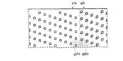
図17はインターロッキング・グリッドの概念を示す。この図は二つのグレイ・グループ・ストライプb14,b24間の境界域の詳細を示し、簡略にする目的で、4×3アレイを描いている。アパーチャのオフセットを二つのストライプb14,b24間に示している。いずれの構成もストライプb14,b24の下方内部エッジ内に示した正方形画素のグリッドgd14,gd24を規定する。この図から明瞭にすると、二つのグリッドが互いに関してインターロックされる。ストライプb14の構成が連続しておれば、ストライプb24の域内にあるアパーチャの配列をハッチングされた正方形として示している。
ストライプa24内のアパーチャ(すなわち、ブランク開口部)は、他のストライプa14内のアパーチャの位置に関して垂直方向と水平方向にアパーチャ幅の半分だけシフトされる。この結果として、効果的なグリッドが両グリッドgd14,gd24の重畳から得られ、効果的グリッドのピッチはベース・グリッドのピッチの半分になる。異なるグリッドに属するブランク開口部が分離したグレイ・グループとしてアドレスされる。
FIG. 17 illustrates the concept of an interlocking grid. This figure shows details of the boundary area between the two gray group stripes b14, b24, and for the sake of simplicity, depicts a 4 × 3 array. The aperture offset is shown between the two stripes b14 and b24. Both configurations define square pixel grids gd14 and gd24 shown in the lower inner edges of the stripes b14 and b24. For clarity from this figure, the two grids are interlocked with respect to each other. If the configuration of the stripe b14 is continuous, the arrangement of the apertures within the area of the stripe b24 is shown as a hatched square.
The aperture (ie, the blank opening) in the stripe a24 is shifted by half the aperture width in the vertical and horizontal directions with respect to the position of the aperture in the other stripe a14. As a result, an effective grid is obtained from the superposition of both grids gd14, gd24, and the pitch of the effective grid is half that of the base grid. Blank openings belonging to different grids are addressed as separate gray groups.
インターロッキング・アレイは空間画素補間、従って画像配置と線エッジの粗さに関して改善された融通性を許容する。このプロシージャにより、事前規定アドレス・グリッドに対するグレイ・レベルの必要数は、相当低減される。この点は統計的線量ふらつき(ショット・ノイズ)による線量変化がパターン配置とCD制御のために必要とされる線量精度の範囲にあるかどうかが特に重要である。ある一定の露光線量とスポット・サイズに対して、限定されたレベル数のみが統計的に区別可能である(例えば、25nm正方形スポットと1電子/nm2露光線量に対して約30レベルのみ)。インターロッキング・グリッドは既存の画素代表を補間して、例えばグレイ・レベルの必要数を低減し、―PDフィールドのダウンスケールが望まれるときに重要になる―または小さいアドDレス・グリッドを使用することで解像度を改善し、―例えばトランジスタ・ゲートのような最も限界的な線に対して使用することができる。任意のグレイ画素データのための直線保管インターロッキング・グリッドの計算のような必要とするデータ事前計算が操作中またはオフラインで実行することができる。 The interlocking array allows improved flexibility with respect to spatial pixel interpolation and thus image placement and line edge roughness. This procedure significantly reduces the required number of gray levels for the predefined address grid. This point is particularly important if the dose variation due to statistical dose fluctuation (shot noise) is within the range of dose accuracy required for pattern placement and CD control. For a given exposure dose and spot size, only a limited number of levels are statistically distinguishable (eg, only about 30 levels for a 25 nm square spot and 1 electron / nm 2 exposure dose). The interlocking grid interpolates existing pixel representatives, for example, to reduce the required number of gray levels-becoming important when downscaling of the PD field is desired-or using a small add-Dless grid This improves resolution and can be used for the most critical lines, such as transistor gates. Necessary data pre-calculations such as linear storage interlocking grid calculations for arbitrary gray pixel data can be performed during operation or offline.
直接書き取りリトグラフ内のグレイ・スケールにおける必要性は、画像配置と線エッジ粗さに関する仕様と一致させるために、半導体工業デザイン規則がますます小さくなるアドレス・グリッドを暗示していることから発していることが喚起される。例えば、約22.5nmのぼやけと25nmピッチのアドレス・グリッドを有する幾何学的スポット・サイズを使用して、46のグレイ・レベルを示すシミュレーションが、ウェハ上に1nmの必要精度で構成を配置するのに充分である(線配置エラーが全グリッド位置で0.5nm以下の線位置エラーと、0.5nm以下の線幅エラーを意味する)。付加的に、リトグラフ仕様と一致させるために、総合線幅変動が限界寸法の約10%未満(=公称最小線幅)である。これは単一サイド線エッジ粗さが線幅の5%未満であることを意味している。線エッジ粗さは、閾値線量でカットオフ後、露光ウェハ(空間画像)で総合線量分布のレベル・カーブの直線bの偏差によって表わされる線の直線性のための測定値である。 The need for gray scale in direct write lithographs stems from the fact that the semiconductor industry design rules imply an increasingly smaller address grid to match the specifications for image placement and line edge roughness. Is aroused. For example, using a geometric spot size with a blur of about 22.5 nm and an address grid of 25 nm pitch, a simulation showing 46 gray levels places the configuration on the wafer with the required accuracy of 1 nm. (Line arrangement error means a line position error of 0.5 nm or less and a line width error of 0.5 nm or less at all grid positions). Additionally, the total line width variation is less than about 10% of the critical dimension (= nominal minimum line width) to match the lithographic specification. This means that the single side line edge roughness is less than 5% of the line width. The line edge roughness is a measurement value for the linearity of a line represented by the deviation of the line b of the level curve of the total dose distribution on the exposure wafer (spatial image) after being cut off at the threshold dose.
インターロッキング―グリッド・グレイ画素の主たる利点は次の通りである。 Interlocking-The main advantages of grid gray pixels are:
1)グレイ・レベルの同じ数で高揚された配置制度
2)任意のアドレス・グリッドに対して必要とするグレイ・レベルが相当低減
3)グレイ・レベル数の低減がPDフィールドのサイズのさらなる低減を許容
4)最も限界的な線(解像度<ノード)の書き取りが同じ走査速度で可能
5)任意のぼやけ(最小外径サイズのパーセント)に対して、小さいリトグラフ・ノードが達成
6)ブランク・アパーチャ・プレート内の総アパーチャの限定数に対して、小さい直径カラムの場合に、レベル当りのアパーチャ数(=冗長性)従来のグリッドと比べてインターロッキング・グリッドに対してより高い、16.2mmの矩形プレートの例によって説明すると、90個のアパーチャがインターロッキング・グリッドを使用してまたはそれぞれインターロッキング・グリッドなしに46個のグレイ・レベル(1レベル当り2アパーチャ)を使用して2×16のグレイ・レベル(1レベル当り3アパーチャ)に副分割することができる。
1) Placement scheme enhanced with the same number of gray levels 2) Significant reduction in gray levels required for any address grid 3) Reduction in number of gray levels further reduces PD field size Tolerance 4) The most critical line (resolution <node) can be written at the same scan speed 5) Small lithographic nodes achieved for any blur (percentage of minimum outer diameter size) 6) Blank aperture For a limited number of total apertures in the plate, for small diameter columns, the number of apertures per level (= redundancy), a 16.2 mm rectangle that is higher for the interlocking grid compared to the conventional grid Illustrated by the example of a plate, 90 apertures can be interlocked using an interlocking grid or each It can be subdivided without Kkingu grid using the 46 gray levels (1 level per second aperture) to the gray level of 2 × 16 (1 level per 3 apertures).
図18は図8のグリッドと同様に示したように、インターロッキング・グリッドを備えたPDフィールド実行グレイ・グループを示す。コンバータ手段821…824がPDフィールドを取り囲んでおり、フィールド内でブランク開口部のグレイ・グループが実行され、またグレイ・グループがここでも(図8と同様に)ストライプa11,a12,a13,a14,a21,a22,a23,a24に組織化され、PDフィールドの幅が走査方向を横断してスパンされる。しかし、この場合において、最初の四つのストライプa11…a14が第一ドメインdm1に、一方他の四つのストライプa21…a24が第二ドメインdm2に属し、グリッド・シフトがアパーチャに対応する正方形の対角線の半分だけシフトされてグリッドが実現する。従って、図17を参照してこれまでに詳述し検討したように第一dm1のストライプa11…a14の下方にあるグリッドは第二dm2のストライプでインターロッキングされる。 FIG. 18 shows a PD field execution gray group with an interlocking grid as shown in the same manner as the grid of FIG. Converter means 821... 824 surround the PD field and a gray group of blank openings is performed in the field, and the gray group is again (as in FIG. 8) stripes a11, a12, a13, a14, Organized into a21, a22, a23, a24, the width of the PD field is spanned across the scanning direction. However, in this case, the first four stripes a11... A14 belong to the first domain dm1, while the other four stripes a21... A24 belong to the second domain dm2, and the grid shift is a square diagonal line corresponding to the aperture. The grid is realized by shifting by half. Thus, as detailed and discussed above with reference to FIG. 17, the grid below the first dm1 stripes a11... A14 is interlocked with the second dm2 stripes.
従って、各ドメインdm1,dm2はブランク開口部の複数の折れ線からなり、一つのドメインの線は線の幅の一部だけ他のドメインの線に対してオフセットし、各ドメインの各線のアパーチャは少なくとも一つのグループを表わしている。図18に示す特定の場合において、二つのドメインはグループの対応する仕切りを有しており、これによって第一ドメインの各グループはそれぞれのグループ内にブランク開口部の等数を有する第二ドメインの対応するグループを有している。しかし、本発明の概念内の変形は充分可能であり、一つのドメイン内のアパーチャ数またはグループへの仕切りは別のドメイン内で使用されるものとは異なる。第二ドメインのために完全な実行はいずれの場合においても必要でないことが予想されるが、主要グループはターゲット上に微細な空間解像度を形成するために適切な中間強度を実現する。 Therefore, each domain dm1, dm2 is composed of a plurality of broken lines of blank openings, and one domain line is offset from the other domain lines by a part of the line width, and the aperture of each line of each domain is at least It represents one group. In the specific case shown in FIG. 18, the two domains have corresponding partitions of the group, whereby each group of the first domain is a second domain having an equal number of blank openings within each group. Has a corresponding group. However, variations within the concept of the invention are quite possible, and the number of apertures in one domain or partitioning into groups is different from that used in another domain. Although it is expected that full execution is not necessary in any case for the second domain, the main group achieves the appropriate intermediate intensity to form a fine spatial resolution on the target.
図18のPDデバイスのアパーチャの配列は、n=6とm=6(n×m=36)に基づいた配列内で90×3240のアパーチャからなる。ウェハ上で照明される画素サイズ(図3で素幅x)は、図示実施例に使用された200×低減光学系と5μmアパーチャに基づいて25nmである。ストライプa11…a14,a24…a21のグレイ・グループ内のアパーチャ数は、図18の左から右へ(3,6,12,24;24,12,6,3)である。より明瞭にするために、アパーチャ・マークは図18では示していない。他の観点において、図8で考慮した同じ事項は図18においても適用する。 The aperture arrangement of the PD device in FIG. 18 is composed of 90 × 3240 apertures in an array based on n = 6 and m = 6 (n × m = 36). The pixel size illuminated on the wafer (element width x in FIG. 3) is 25 nm based on the 200 × reduction optics and 5 μm aperture used in the illustrated embodiment. The number of apertures in the gray group of the stripes a11... A14, a24... A21 is from left to right (3, 6, 12, 24; 24, 12, 6, 3) in FIG. For clarity, the aperture marks are not shown in FIG. In other respects, the same considerations considered in FIG. 8 also apply in FIG.
インターロッキング・グリッドを実現する他の方法があることに注意する価値がある。一例を図19と20に示す。すなわち、三角形ターゲット・グリッド(図20)にアドレスするためのPDフィールド(図19)における六角アパーチャ(または六角形に近似した形状、例えば円形または角の丸くなった方形を有するのも)である。アパーチャ(またはブランク開口部)は、三つのドメインhm1,hm2,hm3内に配列される。上述の考慮に基づいてグレイ・グループに副分割できる各ドメイン内で、アパーチャは六角形アレイ(走査方向に延長される)に基づく互いの関係で配置され、ここで近接線は六角形の辺の長さの3/2だけ隔置され、また近接線内のアパーチャのオフセットhoに対して適した値は、ho=(k+1/2)・a・√3であり、ここにk>1は整数である。概して、適切な信号位相変換がオフセット線に対して提供されればどのオフセットも可能である。異なるドメインd12とd23のアパーチャ間の距離はオフセットhoまたは(k’+1/2)・a・√3として等しく選択でき、あるいは一般的に、適切な信号位相変換がそれぞれのドメインに属するグループの第一アパーチャに適用されれば、どのオフセットとすることができる。距離d12とd23は、通常互いに等しいが、異なる値をとることもできる。これらの値で、図19の六角アパーチャは図20に示した三角形ターゲット・グリッドhgに基づく規則的な分布を発生させるために適している。この図において、ドットはターゲット(露光ドットの中心)上の物理的アクセス・グリッドを表わしており、また実線は全三つのドメインhm1…hm3のアパーチャの幾何学的スポットの包絡線を表わしている。 It is worth noting that there are other ways to implement an interlocking grid. An example is shown in FIGS. That is, the hexagonal aperture in the PD field (FIG. 19) for addressing the triangular target grid (FIG. 20) (or a shape approximating the hexagon, eg, having a rounded or rounded square). The apertures (or blank openings) are arranged in three domains hm1, hm2, hm3. Within each domain that can be subdivided into gray groups based on the above considerations, the apertures are arranged in relation to each other based on a hexagonal array (extending in the scan direction), where the proximity lines are hexagonal edges. A suitable value for the offset ho of the aperture in the proximity line, separated by 3/2 of the length, is ho = (k + 1/2) · a · √3, where k> 1 is an integer It is. In general, any offset is possible if an appropriate signal phase transformation is provided for the offset line. The distance between the apertures of the different domains d 12 and d 23 can be chosen equally as an offset ho or (k ′ + 1/2) · a · √3, or in general a group in which the appropriate signal phase transformation belongs to the respective domain Any offset can be used if applied to the first aperture. The distance d 12 and d 23 is usually equal to each other, it may take different values. With these values, the hexagonal aperture of FIG. 19 is suitable for generating a regular distribution based on the triangular target grid hg shown in FIG. In this figure, the dots represent the physical access grid on the target (the center of the exposed dot), and the solid lines represent the envelopes of the geometric spots of the apertures in all three domains hm1 ... hm3.
リトグラフe−ビーム直接書き取りアプリケーションのためのインターロッキング・グリッドの特定する利点は、次の考えによる。 The particular advantage of an interlocking grid for lithographic e-beam direct write applications is due to the following considerations.
リトグラフ内で最高解像度を達成するのに適した高電圧電子ビーム・リトグラフに対して、特に100keV電子が使用されたときに、望まない線量寄与(近似効果)がウェハ(すなわち、ターゲット)からの電子後方散乱によってもたらされる。普通100keV後方散乱電子が、レジストで覆われた面に到達する前方約30μmの寸法に実質的に放射される。これと比較して、低エネルギーで優勢である前方散乱はあまり重要でない寄与のみを生ぜしめる。100keV電子によってもたらされた近似効果のために修正すると、問題はスムーズな背景線量修正に変換することができ、また特定構造形状と実質上無関係である。 For high voltage electron beam lithographs suitable for achieving the highest resolution within the lithograph, especially when 100 keV electrons are used, unwanted dose contributions (approximate effects) cause electrons from the wafer (ie, target). Caused by backscattering. Usually 100 keV backscattered electrons are emitted substantially to a dimension of about 30 μm forward reaching the resist-covered surface. Compared to this, forward scattering, which predominates at low energy, only produces a less important contribution. When corrected for the approximate effect brought about by 100 keV electrons, the problem can be translated into a smooth background dose correction and is substantially independent of the specific structural shape.
例えば、シリコン内の100keV電子の後方散乱は、最大50%パターン密度が仮定された場合、レジスト内に溶着された線量(平均して30μm以上)の約14%のエキストラ線量を引き起こす。非常に低いパターン密度に対して、例えば隣にパターンのない離れた線の場合において、後方散乱は総線量に対してそんなに重要な役割を演じることはない。 For example, backscattering of 100 keV electrons in silicon causes an extra dose of about 14% of the dose deposited in the resist (on average 30 μm or more) assuming a maximum 50% pattern density. For very low pattern densities, for example in the case of a disjoint line with no pattern next to it, backscatter does not play that important role for the total dose.
本発明によって可能となる近似修正のための有効な計画は、エッジ・スロープの調整と総線量分布(=溶着線量+後方散乱によるエキストラ線量)のカットオフ位置の調整である。これには適切なグレイ・レベルによるインターロッキング−グリッド・グレイ・レベル点を使用する。全体のアドレス・グリッドに渡る最適化エッジ・スロープで付加設計されたエッジ位置を生成する。 An effective plan for the approximate correction made possible by the present invention is the adjustment of the edge slope and the cut-off position of the total dose distribution (= welding dose + extra dose due to backscattering). This uses interlocking-grid gray level points with appropriate gray levels. Generate edge positions additionally designed with optimized edge slopes across the entire address grid.
インターロッキング・グリッドの説明した方法は、非常に微細なアドレス・グリッド(線位置、線幅)を許容し、その全構成は実際に同じ処理寛容度で実行することができる。ゼロ背景であるが、14%背景も存在する場合において、溶着エネルギー・プロフィールとカットオフ位置のエッジ・スロープの調整が可能であり、ローカル・パターン密度と無関係の全グリッドに対して充分な大きさの処理寛容度を許容する。 The described method of interlocking grid allows a very fine address grid (line position, line width), and its entire configuration can actually be implemented with the same processing latitude. In the case of zero background but also 14% background, the welding energy profile and the edge slope of the cut-off position can be adjusted and are large enough for all grids independent of local pattern density Allow for processing latitude.
共通の高コントラスト・レジスト材料に対して、解像度および処理寛容度が大気画像(溶着線量の空間分布)から導出される。化学的に増大されたレジストのための共通点として、潜像(すなわち、露光されたレジストおよび未露光のレジストの空間分布)は、大気画像の負密度の指数に比例する。得られたガンマ状特性は、リトグラフ処理がある一定線量レベルで通常最大線量レベルの半分で大気画像を「カットオフ」することによって導出することができた後、共通の(また優れた)近似値につながる。次に示す例において、線量分布は平均線量レベルの50%でカットオフされ、本発明によって提供された新しい可能性を使用して開発後、線の達成可能幅および位置に対する印象をリーダに与える。 For common high-contrast resist materials, resolution and processing latitude are derived from atmospheric images (spatial distribution of deposition dose). As a common point for chemically enhanced resists, the latent image (ie, the spatial distribution of exposed and unexposed resist) is proportional to the negative density index of the atmospheric image. The resulting gamma-like characteristics can be derived by “cutting off” the atmospheric image at a certain dose level at a fixed dose level and usually half of the maximum dose level, then a common (and excellent) approximation Leads to. In the following example, the dose distribution is cut off at 50% of the average dose level, giving the reader an impression of the achievable width and position of the line after development using the new possibilities provided by the present invention.
説明の都合上、上述例にインターロッキング・グリッドを使用したと仮定して、三つの任意に選択されたグリッド位置に対するターゲット上に作像された線特性のためにシミュレートされた線量分布(大気画像)をゼロ背景につき図23a−cに、また14%背景につき図23d−fに示す。図23および24において、実線は総線量を表わし、また破線は線(線は充分長く線の端部がセクションに寄与しないと仮定)の断面に沿ったそれぞれの総線量に対するここのグレイ画素(ガウス形状)の寄与を表わしている。近似効果に関連する背景の最悪ケースを説明するために、全曲線はエリア当り総線量の14%だけシフトされており、上方向は図23d−f(50%パターン密度の場合および後方散乱による28%線量分布)である。明らかに、0%と14%背景間で同様の特性が見つかった。 For convenience of explanation, assuming that an interlocking grid was used in the above example, a simulated dose distribution (atmosphere) for the line characteristics imaged on the target for three arbitrarily selected grid positions. Image) is shown in FIGS. 23a-c for zero background and in FIGS. 23d-f for 14% background. In FIGS. 23 and 24, the solid line represents the total dose, and the dashed line represents the gray pixel (Gaussian) for each total dose along the cross-section of the line (assuming that the line is long enough not to contribute to the section). Shape) contribution. To illustrate the background worst case associated with the approximate effect, the entire curve is shifted by 14% of the total dose per area, and the upward direction is shown in FIGS. 23d-f (50% pattern density and 28 due to backscattering). % Dose distribution). Obviously, similar characteristics were found between 0% and 14% background.
比較の目的で、インターロッキング・グリッドなしで、46またはさらにそれ以上のグレイ・レベル(二つのドメインに対して16+16の代わりに)を使用したことが微細傾斜角度調整をほとんど許容しない。ゼロ背景につき図24a−cのシミュレーションに示し、また14%の背景につき図24d−fに示す。本質的に、特に1nm未満の精度が必要とされれば、インターロッキング・グリッドは傾斜角度調整と線配置制御両方を同時に達成するのに必要とされる。図23a−fで証明したようにエッジ傾斜とカットオフ位置の全体的微調整は重なり領域の内部の線量分布を制御する可能性によって可能となる。 For comparison purposes, using 46 or even more gray levels (instead of 16 + 16 for two domains) without an interlocking grid would allow very little fine tilt angle adjustment. A zero background is shown in the simulation of FIGS. 24a-c and a 14% background is shown in FIGS. 24d-f. In essence, the interlocking grid is required to achieve both tilt angle adjustment and line placement control simultaneously, especially if accuracy below 1 nm is required. As demonstrated in FIGS. 23a-f, the overall fine adjustment of the edge slope and cut-off position is made possible by the possibility of controlling the dose distribution inside the overlap region.
次に適用される処理寛容度(または線量寛容度)に対する一つの量的表現は、公称線幅の変化が90%から110%を生じる線量ウィンドウとなる。処理寛容度の典型的な値は、ぼやけが最小構造サイズの半分であれば、ほぼ15%である。本発明によるインターロッキング・グレイ画素を使用して出願人によってなされた計算が示しているのは、処理寛容度が0%から14%(0−50%のパターン密度に対応)までの全グリッド位置および可変背景に対して約14.5に保持でき、一方インターロッキング・グリッドなしでほぼ2の要素によってグリッド位置を伴う処理寛容度の明白な変化がある。一例として、45nmノードを達成可能な処理寛容度は図25aのインターロッキング・グリッドのために与えられ、インターロッキング・グリッドのないのが図25bである。 One quantitative expression for the next applied treatment latitude (or dose tolerance) is a dose window where the change in nominal line width results in 90% to 110%. A typical value for processing latitude is approximately 15% if the blur is half the minimum structure size. Calculations made by Applicants using interlocking gray pixels according to the present invention show all grid positions from 0% to 14% processing latitude (corresponding to 0-50% pattern density). And about 14.5 for variable background, while there is an obvious change in processing latitude with grid position by approximately two elements without an interlocking grid. As an example, the processing latitude that can achieve a 45 nm node is given for the interlocking grid of FIG. 25a, and FIG. 25b without the interlocking grid.
これまでに説明したように、PDフィールド内のアパーチャの全数(またはグレイ・レベル)は、図25bと比較して図25aの線量寛容度の改善による例で示され、本発明によるインターロッキング・グリッドを使用することによって低減される。全てのグレイ・グループのアパーチャの最小数は、45レベルで45アパーチャを有する一つのドメインと比較して各16レベルを有する2ドメインに対して1+2+4+8+8+4+2+1=30のアパーチャである。結果として、本発明は小さいビーム直径を有する光学カラムの使用を可能にし、線内のアパーチャの数を少なくしている。小さい直径のカラムを使用しマルチカラム・アプローチを実現してウェハの生産量を高めるとともにステージ・パラメータを低減する。 As explained so far, the total number (or gray level) of apertures in the PD field is shown in the example by the improved dose tolerance of FIG. 25a compared to FIG. 25b, the interlocking grid according to the invention. Is reduced by using. The minimum number of apertures in all gray groups is 1 + 2 + 4 + 8 + 8 + 4 + 2 + 1 = 30 apertures for 2 domains with 16 levels each compared to one domain with 45 apertures at 45 levels. As a result, the present invention allows the use of optical columns with small beam diameters and reduces the number of apertures in the line. Use a small-diameter column to implement a multi-column approach to increase wafer production and reduce stage parameters.
構造形状とパターン密度と無関係にある処理寛容度を実現する可能性は、半導体製造業界に関する本発明の主要な利点である。実際に、リトグラフ・コントラスト、従って露光の歩止まりが処理寛容度に密接に関連があり、露光線量が公称露光線量に関して変化すれば、処理関連の限界寸法変動に対する測定値となる。グリッド位置上の処理寛容度のいかなる依存度も利用できる処理寛容度の低減を意味し、全ウェハが同じ条件下で処理されなければならない。従来技術において、走査ストライプ露光計画内の近似修正が全処理寛容度の低減と避けられない関係にあって、例え複数のグレイ・レベルを使用したとしてもである。 The possibility of achieving processing latitude that is independent of structure shape and pattern density is a major advantage of the present invention for the semiconductor manufacturing industry. Indeed, lithographic contrast, and hence exposure yield, is closely related to process latitude, and if exposure dose varies with respect to nominal exposure dose, it is a measure for process related critical dimension variations. Any dependency of the processing latitude on the grid location means a reduction in processing latitude that can be used, and all wafers must be processed under the same conditions. In the prior art, the approximate correction in the scanning stripe exposure plan is unavoidably related to the reduction in overall processing latitude, even if multiple gray levels are used.
確かに、後方散乱以外に前方散乱の修正も原則としてインターロッキング・スポットの使用によって達成される。プロシージャは簡単である。 Certainly, in addition to backscattering, forward scattering correction is in principle also achieved through the use of interlocking spots. The procedure is simple.
インターロッキング・グリッドを使用する別の重要な利点は、閾値レベルでのカットオフ後の空間線量分布のレベル曲線が非常に滑らかになり、従って得られた線エッジ粗さが非常に小さくなることである。インターロッキング・グリッドを使用したものと使用しないものとの間の線エッジ粗さ(片側)の比較(発明者によってシミュレートした)は本明細書の最後に記す表1に示した。インターロッキング・グリッドのない場合に対して、片側線エッジ粗さの最大値は、グリッドに関して45゜の角度で線に対して線幅の4.32%である。これはリトグラフ条件、すなわち、総線幅変化が線幅の10%未満であることを意味し、このケースと一致することはほとんどない。概して、線エッジ粗さはレジスト処理とショット・ノイズから付加的な寄与を得る。両者は許容された10%内に含まれる。本発明に基づくインターロッキング・グリッドを伴う同じPDを使用して、例えば32nmの解像度であっても線エッジ粗さは充分小さく維持され、グリッドに関して20゜で1.88%のシミュレートされた最大値となる。 Another important advantage of using an interlocking grid is that the level curve of the air dose distribution after cut-off at the threshold level is very smooth and thus the resulting line edge roughness is very small. is there. A comparison of line edge roughness (one side) between using and not using an interlocking grid (simulated by the inventor) is shown in Table 1 at the end of this specification. For the case without an interlocking grid, the maximum value for one-sided line edge roughness is 4.32% of the line width relative to the line at an angle of 45 ° with respect to the grid. This means that the lithographic condition, i.e. the total line width change is less than 10% of the line width, which is rarely consistent with this case. In general, line edge roughness derives an additional contribution from resist processing and shot noise. Both are included within the allowed 10%. Using the same PD with an interlocking grid according to the present invention, the line edge roughness is kept small enough, for example at 32 nm resolution, with a simulated maximum of 1.88% at 20 ° with respect to the grid Value.
最終的に、図26a,26bおよび27は、処理寛容度の低減絶対値を受容すること示しており、インターロッキング・グリッドの使用が図23と24で使用された同じ22.5nmのぼやけで32nm線の発生も許容し、さらに可変背景線量が0%と14%の間である。ここでもまた処理寛容度が線位置と無関係になるように調整でき、また線中心と線幅エラーが全1nmアドレス・グリッドに渡って0.5nm未満であり(ドメイン当り16レベルを使用したシミュレーションによる)、同じPDデバイスが原則として32nm線と空間解像度に対して使用できる。これはインターロッキング・グリッドが、インターロッキング・グリッドなしで画像ぼやけによってもたらされる制限のずっと下方に解像度がなることを許容し、また例えば特徴サイズの70%のぼやけで32nm特徴に達することを許容する。 Finally, FIGS. 26a, 26b and 27 show that it accepts a reduced absolute value of processing latitude, and the use of an interlocking grid is 32 nm with the same 22.5 nm blur used in FIGS. Lines are also allowed, and the variable background dose is between 0% and 14%. Again, processing latitude can be adjusted to be independent of line position, and line center and line width errors are less than 0.5 nm across the entire 1 nm address grid (by simulation using 16 levels per domain). ), The same PD device can in principle be used for 32 nm lines and spatial resolution. This allows the interlocking grid to reach a resolution far below the limit introduced by image blur without the interlocking grid, and to reach 32 nm features, for example with 70% blur of feature size. .
本発明は明らかにPDデバイス内の製造制限を回避する助けをし、究極の解像度に関する作像システムの最高の開発を可能にする。低パターン密度で45nmノードに対して、相当な背景は何も存在せず、45nm線に関する限り同じ値まで32nmの線量寛容度を増大させることが可能である。この可能性は例えば45nmリトグラフ処理の低減幅(32nm線)、例えばトランジスタのゲート長さの書き取り限界線に使用することができる。 The present invention clearly helps to avoid manufacturing limitations in PD devices and allows the best development of imaging systems for the ultimate resolution. For a 45 nm node at low pattern density, there is no significant background and it is possible to increase the 32 nm dose tolerance to the same value as far as the 45 nm line is concerned. This possibility can be used, for example, for the write-down limit line of 45 nm lithographic processing reduction width (32 nm line), eg transistor gate length.
インターロッキング・グリッドの原理は、パターンがグレイ画素で構成されるあらゆる種類のパターン発生、特に(しかし、これに限定しない)合焦イオン・ビームまたは電子ビーム直接書き取りアプリケーションに使用できることを説明する価値がある。本発明の別のアプリケーションは、例えば光学マスクレス・リトグラフへのインターロッキング・グリッドの使用であって、光またはX線ビームがアドレス可能ミラー・プレートによって構成され、また基板へ直接向けられる。 The interlocking grid principle is worth explaining that it can be used for all kinds of pattern generation where the pattern is composed of gray pixels, especially (but not limited to) focused ion beam or electron beam direct write applications. is there. Another application of the present invention is the use of an interlocking grid, for example for optical maskless lithographs, where the light or x-ray beam is constituted by an addressable mirror plate and is directed directly to the substrate.
要約すると、インターロッキング・グリッドの主な利点は、
1)グレイ・レベルの低い数が必要:主な改良の一つは単一走査ストライプ露光処理中に可能な物理的アドレス・グリッドの低減(すなわち、近接露光スポットの距離)である。これはPDフィールド上方に適切な方法でアパーチャの利用可能数を配列し、(補間された画素情報で)適切に変換されたデータ流れによるアパーチャの一部をアドレスすることによって達成される。対応するアドレス・グリッドおよび処理寛容度が、物理的アドレス・グリッドが倍化されて各露光スポットに対するグレイ・レベルの低い数にもかかわらず相当改善される。例えば、12.5nm距離(XおよびY方向に)でインターロッキング・グリッド・スポットと各スポットに対して16グレイ・レベルを有する25nm幅の露光スポットを使用することで、1nmアドレス・グリッド(線の中心のエラー<0.5nm、線の幅のエラー<0.5nm)が、14.6%処理寛容度の優れた線量寛容度で実現することができる。比較の目的で、露光スポット当り64グレイ・レベルさえもないインターロッキング・グリッドなしで、処理寛容度が係数2だけグリッド位置で変化すると、比較的低い処理寛容度を満足させない。
In summary, the main benefits of interlocking grids are:
1) A low number of gray levels is required: One of the main improvements is the reduction in physical address grid that is possible during the single scan stripe exposure process (ie, the distance of the close exposure spot). This is accomplished by arranging the available number of apertures in the appropriate way above the PD field and addressing the part of the aperture with the appropriately transformed data stream (with interpolated pixel information). Corresponding address grid and processing latitude are significantly improved despite the low number of gray levels for each exposure spot with the physical address grid doubled. For example, using an interlocking grid spot and a 25 nm wide exposure spot with 16 gray levels for each spot at a 12.5 nm distance (in the X and Y directions), a 1 nm address grid (line A center error <0.5 nm, line width error <0.5 nm) can be achieved with an excellent dose tolerance of 14.6% treatment latitude. For comparison purposes, a relatively low processing latitude is not satisfied if the processing latitude is changed at the grid position by a factor of 2 without an interlocking grid with even 64 gray levels per exposure spot.
2)近似修正可能性:別の利点はいくつかの露光スポットを重ねることによって広い範囲内でスロープ角度とスロープ位置を調整することの可能性に関係し、これによって近似効果関連背景線量が、線量寛容度内の変化に至ることもなく、非常に小さいアドレス・グリッドに渡り達成できる線位置および線幅を低減することもない。 2) Approximate correctability: Another advantage relates to the possibility of adjusting the slope angle and slope position within a wide range by overlaying several exposure spots, so that the approximate effect related background dose is It does not lead to changes within tolerance, nor does it reduce the line position and line width that can be achieved over very small address grids.
3)高揚された解像度:第3の利点は高いスロープ角度で構成を形成することによって画像コントラストを相当改善する可能性に基づいている。これが任意の収差ぼやけのための画像解像度の効果的な高揚に至る。例えば、5μmアパーチャと200×縮小を使用して、対応する露光スポットが32nmの画像線解像度を、さらに1nmアドレス・グリッド上に高い処理寛容度を許容する。 3) Enhanced resolution: The third advantage is based on the possibility of significantly improving the image contrast by forming the structure with a high slope angle. This leads to an effective enhancement of the image resolution for any aberration blur. For example, using a 5 μm aperture and 200 × reduction, the corresponding exposure spot allows a 32 nm image line resolution and a higher processing latitude on a 1 nm address grid.
ターゲット画素の微細グリッドをアドレスする別の可能な方法を図21に示す。異なるグループのためのアパーチャの異なるサイズによる構成は、特定チャネルの解像度または強度寄与を増大するのに使用できる。ストライプa11のグループのアパーチャは線の幅よりも小さく、一方他のストライプa01,a02に属するグループのアパーチャは線の幅(「標準サイズ」)に対応している。もちろん、アパーチャの種々の形状を含めて前述の変形例の組み合わせも考慮できる。 Another possible way of addressing the fine grid of target pixels is shown in FIG. Configurations with different sizes of apertures for different groups can be used to increase the resolution or intensity contribution of a particular channel. The aperture of the group of stripes a11 is smaller than the line width, while the apertures of the groups belonging to the other stripes a01 and a02 correspond to the line width (“standard size”). Of course, combinations of the above-described modified examples including various shapes of the aperture can also be considered.

Claims (8)
複数のブランク開口部を有するマルチアパーチャ・プレートであって、それぞれのブランク開口部が、第1の状態と第2の状態との間で、ブランク信号によって制御可能な偏向電極を含み、前記第1の状態において、前記ブランク開口部を通って放射する前記帯電粒子のビームの粒子が、所定の経路に沿って進み、前記第2の状態において、前記ブランク開口部を通って放射する前記帯電粒子のビームの粒子が、前記所定の経路を外れて偏向される、マルチアパーチャ・プレートとを備えた帯電粒子ビーム露光装置であって、
前記ブランク開口部の複数のグループは、それぞれのグループが複数のブランク開口部を有するように形成され、それぞれのグループの前記ブランク開口部の対は、電気遅延素子によって互いに電気的に接続され、共通のグループ・ブランク信号によって制御されることを特徴とする帯電粒子ビーム露光装置。 A charged particle source that generates a beam of charged particles;
A multi-aperture plate having a plurality of blank openings, each blank opening including a deflection electrode controllable by a blank signal between a first state and a second state, wherein the first In this state, the particles of the charged particle beam radiating through the blank opening travel along a predetermined path, and in the second state, the charged particle radiating through the blank opening. A charged particle beam exposure apparatus comprising a multi-aperture plate, wherein beam particles are deflected off said predetermined path,
The plurality of groups of blank openings are formed such that each group has a plurality of blank openings, and the pairs of blank openings in each group are electrically connected to each other by an electrical delay element The charged particle beam exposure apparatus is controlled by a group blank signal.
A wafer stage for mounting a wafer, and configured to direct the particles of the beam of charged particles that radiate through the blank opening and travel along a predetermined path on the wafer attached to the wafer stage charged particle beam exposure apparatus according to any one of claims 1 to 7 further comprising a charged particle optical system.
Applications Claiming Priority (2)
| Application Number | Priority Date | Filing Date | Title |
|---|---|---|---|
| ATA755/2004 | 2004-04-30 | ||
| AT7552004 | 2004-04-30 |
Publications (3)
| Publication Number | Publication Date |
|---|---|
| JP2005328047A JP2005328047A (en) | 2005-11-24 |
| JP2005328047A5 JP2005328047A5 (en) | 2008-05-29 |
| JP4843248B2 true JP4843248B2 (en) | 2011-12-21 |
Family
ID=34658437
Family Applications (1)
| Application Number | Title | Priority Date | Filing Date |
|---|---|---|---|
| JP2005134248A Expired - Fee Related JP4843248B2 (en) | 2004-04-30 | 2005-05-02 | Improved pattern definition apparatus for particle beam exposure. |
Country Status (3)
| Country | Link |
|---|---|
| US (1) | US7368738B2 (en) |
| JP (1) | JP4843248B2 (en) |
| GB (1) | GB2413694A (en) |
Cited By (3)
| Publication number | Priority date | Publication date | Assignee | Title |
|---|---|---|---|---|
| US9082581B2 (en) | 2013-10-11 | 2015-07-14 | Nuflare Technology, Inc. | Blanking device for multiple charged particle beams |
| US9190238B2 (en) | 2013-11-12 | 2015-11-17 | Nuflare Technology, Inc. | Blanking device for multi charged particle beam, and multi charged particle beam writing method |
| US10133186B2 (en) | 2016-10-20 | 2018-11-20 | Mapper Lithography Ip B.V. | Method and apparatus for aligning substrates on a substrate support unit |
Families Citing this family (60)
| Publication number | Priority date | Publication date | Assignee | Title |
|---|---|---|---|---|
| CN102709143B (en) | 2003-09-05 | 2016-03-09 | 卡尔蔡司Smt有限责任公司 | Electron optics arrangement, polyelectron beam splitting checking system and method |
| US7448012B1 (en) | 2004-04-21 | 2008-11-04 | Qi-De Qian | Methods and system for improving integrated circuit layout |
| WO2006053360A1 (en) * | 2004-11-17 | 2006-05-26 | Ims Nanofabrication Gmbh | Registering device and method for a pattern lock system in a particle-beam exposure apparatus |
| EP1943660B9 (en) * | 2005-10-28 | 2009-09-09 | Carl Zeiss SMS GmbH | Charged particle beam exposure system |
| US7384852B2 (en) * | 2006-10-25 | 2008-06-10 | International Business Machines Corporation | Sub-lithographic gate length transistor using self-assembling polymers |
| US8426832B2 (en) * | 2006-11-21 | 2013-04-23 | D2S, Inc. | Cell projection charged particle beam lithography |
| US7897522B2 (en) * | 2006-11-21 | 2011-03-01 | Cadence Design Systems, Inc. | Method and system for improving particle beam lithography |
| US7772575B2 (en) * | 2006-11-21 | 2010-08-10 | D2S, Inc. | Stencil design and method for cell projection particle beam lithography |
| DE102008010123A1 (en) * | 2007-02-28 | 2008-09-04 | Ims Nanofabrication Ag | Multibeam deflecting array device for maskless particle beam machining |
| NL2001369C2 (en) | 2007-03-29 | 2010-06-14 | Ims Nanofabrication Ag | METHOD FOR MASKLESS PARTICLE BEAMLIGHTING |
| JP5491704B2 (en) | 2007-05-14 | 2014-05-14 | イーエムエス ナノファブリカツィオン アーゲー | Pattern definition device having counter electrode array plate |
| US7958736B2 (en) * | 2007-05-24 | 2011-06-14 | Bio-Rad Laboratories, Inc. | Thermoelectric device and heat sink assembly with reduced edge heat loss |
| ATE527678T1 (en) * | 2008-11-17 | 2011-10-15 | Ims Nanofabrication Ag | METHOD FOR MASKLESS PARTICLE BEAM EXPOSURE |
| EP2190003B1 (en) * | 2008-11-20 | 2014-10-01 | IMS Nanofabrication AG | Constant current multi-beam patterning |
| US8294125B2 (en) * | 2009-11-18 | 2012-10-23 | Kla-Tencor Corporation | High-sensitivity and high-throughput electron beam inspection column enabled by adjustable beam-limiting aperture |
| JP2011199279A (en) * | 2010-03-18 | 2011-10-06 | Ims Nanofabrication Ag | Method for multibeam exposure on target |
| JP2013546180A (en) * | 2010-10-26 | 2013-12-26 | マッパー・リソグラフィー・アイピー・ビー.ブイ. | Modulator and charged particle multi-beam lithography system using the same |
| NL2006868C2 (en) * | 2011-05-30 | 2012-12-03 | Mapper Lithography Ip Bv | Charged particle multi-beamlet apparatus. |
| JP6087570B2 (en) * | 2012-10-15 | 2017-03-01 | キヤノン株式会社 | Drawing apparatus and article manufacturing method |
| JP6215586B2 (en) * | 2012-11-02 | 2017-10-18 | 株式会社ニューフレアテクノロジー | Multi-charged particle beam writing method and multi-charged particle beam writing apparatus |
| JP2014116518A (en) * | 2012-12-11 | 2014-06-26 | Canon Inc | Drawing device and method for manufacturing article |
| EP2757571B1 (en) * | 2013-01-17 | 2017-09-20 | IMS Nanofabrication AG | High-voltage insulation device for charged-particle optical apparatus |
| NL2010760C2 (en) | 2013-05-03 | 2014-11-04 | Mapper Lithography Ip Bv | Beam grid layout. |
| JP6097640B2 (en) * | 2013-06-10 | 2017-03-15 | 株式会社ニューフレアテクノロジー | Multi-charged particle beam writing method and multi-charged particle beam writing apparatus |
| JP2015023286A (en) | 2013-07-17 | 2015-02-02 | アイエムエス ナノファブリケーション アーゲー | Pattern definition device having multiple blanking arrays |
| EP2830083B1 (en) | 2013-07-25 | 2016-05-04 | IMS Nanofabrication AG | Method for charged-particle multi-beam exposure |
| JP6190254B2 (en) * | 2013-12-04 | 2017-08-30 | 株式会社ニューフレアテクノロジー | Multi-charged particle beam writing apparatus and multi-charged particle beam writing method |
| EP2913838B1 (en) | 2014-02-28 | 2018-09-19 | IMS Nanofabrication GmbH | Compensation of defective beamlets in a charged-particle multi-beam exposure tool |
| EP2937888B1 (en) * | 2014-04-25 | 2019-02-20 | IMS Nanofabrication GmbH | Multi-beam tool for cutting patterns |
| EP2937889B1 (en) | 2014-04-25 | 2017-02-15 | IMS Nanofabrication AG | Multi-beam tool for cutting patterns |
| EP3358599B1 (en) | 2014-05-30 | 2021-01-27 | IMS Nanofabrication GmbH | Compensation of dose inhomogeneity using row calibration |
| CN106463347B (en) | 2014-06-13 | 2020-09-15 | 英特尔公司 | In-situ electron beam alignment |
| JP6555619B2 (en) * | 2014-06-13 | 2019-08-07 | インテル・コーポレーション | Data reduction for electron beam throughput |
| CN106463352B (en) * | 2014-06-13 | 2020-06-19 | 英特尔公司 | Unidirectional metal on layer by means of electron beam |
| WO2015191106A1 (en) * | 2014-06-13 | 2015-12-17 | Intel Corporation | Ebeam non-universal cutter |
| KR102389365B1 (en) * | 2014-06-13 | 2022-04-22 | 인텔 코포레이션 | Ebeam universal cutter |
| JP6890373B2 (en) | 2014-07-10 | 2021-06-18 | アイエムエス ナノファブリケーション ゲーエムベーハー | Compensation for imaging deflection in particle beam lithography machines using a convolution kernel |
| EP3183743A4 (en) * | 2014-08-19 | 2018-04-18 | Intel Corporation | Cross scan proximity correction with ebeam universal cutter |
| US9568907B2 (en) | 2014-09-05 | 2017-02-14 | Ims Nanofabrication Ag | Correction of short-range dislocations in a multi-beam writer |
| US9761411B2 (en) * | 2015-01-20 | 2017-09-12 | Taiwain Semiconductor Manufacturing Company, Ltd. | System and method for maskless direct write lithography |
| US9653263B2 (en) | 2015-03-17 | 2017-05-16 | Ims Nanofabrication Ag | Multi-beam writing of pattern areas of relaxed critical dimension |
| EP3096342B1 (en) * | 2015-03-18 | 2017-09-20 | IMS Nanofabrication AG | Bi-directional double-pass multi-beam writing |
| US10410831B2 (en) | 2015-05-12 | 2019-09-10 | Ims Nanofabrication Gmbh | Multi-beam writing using inclined exposure stripes |
| KR102358009B1 (en) * | 2015-11-10 | 2022-02-04 | 삼성전자주식회사 | Beam projection device and method of projecting beam using beam projection device |
| JP2017168574A (en) * | 2016-03-15 | 2017-09-21 | 株式会社ニューフレアテクノロジー | Multi charged particle beam blanking apparatus, multi charged particle beam blanking method, and multi charged particle beam writing apparatus |
| JP6709109B2 (en) * | 2016-05-31 | 2020-06-10 | 株式会社ニューフレアテクノロジー | Blanking device for multi-charged particle beam and multi-charged particle beam irradiation device |
| US10325756B2 (en) | 2016-06-13 | 2019-06-18 | Ims Nanofabrication Gmbh | Method for compensating pattern placement errors caused by variation of pattern exposure density in a multi-beam writer |
| US10325757B2 (en) | 2017-01-27 | 2019-06-18 | Ims Nanofabrication Gmbh | Advanced dose-level quantization of multibeam-writers |
| US10522329B2 (en) | 2017-08-25 | 2019-12-31 | Ims Nanofabrication Gmbh | Dose-related feature reshaping in an exposure pattern to be exposed in a multi beam writing apparatus |
| US11569064B2 (en) | 2017-09-18 | 2023-01-31 | Ims Nanofabrication Gmbh | Method for irradiating a target using restricted placement grids |
| US10651010B2 (en) | 2018-01-09 | 2020-05-12 | Ims Nanofabrication Gmbh | Non-linear dose- and blur-dependent edge placement correction |
| US10840054B2 (en) | 2018-01-30 | 2020-11-17 | Ims Nanofabrication Gmbh | Charged-particle source and method for cleaning a charged-particle source using back-sputtering |
| US10483080B1 (en) * | 2018-07-17 | 2019-11-19 | ICT Integrated Circuit Testing Gesellschaft für Halbleiterprüftechnik mbH | Charged particle beam device, multi-beam blanker for a charged particle beam device, and method for operating a charged particle beam device |
| US10593509B2 (en) | 2018-07-17 | 2020-03-17 | ICT Integrated Circuit Testing Gesellschaft für Halbleiterprüftechnik mbH | Charged particle beam device, multi-beam blanker for a charged particle beam device, and method for operating a charged particle beam device |
| US10978270B2 (en) * | 2018-12-19 | 2021-04-13 | ICT Integrated Circuit Testing Gesellschaft für Halbleiterprüftechnik mbH | Charged particle beam device, interchangeable multi-aperture arrangement for a charged particle beam device, and method for operating a charged particle beam device |
| EP3828914A1 (en) * | 2019-02-27 | 2021-06-02 | FEI Company | Charged particle beam device for inspection of a specimen with a plurality of charged particle beamlets |
| US11099482B2 (en) | 2019-05-03 | 2021-08-24 | Ims Nanofabrication Gmbh | Adapting the duration of exposure slots in multi-beam writers |
| KR20200128363A (en) | 2019-05-03 | 2020-11-12 | 아이엠에스 나노패브릭케이션 게엠베하 | Adapting the duration of exposure slots in multibeam writers |
| KR20210132599A (en) | 2020-04-24 | 2021-11-04 | 아이엠에스 나노패브릭케이션 게엠베하 | Chargedparticle source |
| EP4095882A1 (en) * | 2021-05-25 | 2022-11-30 | IMS Nanofabrication GmbH | Pattern data processing for programmable direct-write apparatus |
Family Cites Families (11)
| Publication number | Priority date | Publication date | Assignee | Title |
|---|---|---|---|---|
| JPS6169125A (en) * | 1984-08-06 | 1986-04-09 | Nippon Telegr & Teleph Corp <Ntt> | Charged beam exposing device |
| US4909864A (en) | 1986-09-16 | 1990-03-20 | Kawasaki Steel Corp. | Method of producing extra-low iron loss grain oriented silicon steel sheets |
| EP0508151B1 (en) | 1991-03-13 | 1998-08-12 | Fujitsu Limited | Charged particle beam exposure system and charged particle beam exposure method |
| JP3194541B2 (en) | 1992-07-24 | 2001-07-30 | 富士通株式会社 | Electron beam exposure system |
| US5369282A (en) * | 1992-08-03 | 1994-11-29 | Fujitsu Limited | Electron beam exposure method and system for exposing a pattern on a substrate with an improved accuracy and throughput |
| JP3678749B2 (en) | 1994-01-13 | 2005-08-03 | アイエムエス イオネン マイクロファブルカティオンズ システメ ゲーエムベーハー | Optical image projection system for particle beams, especially ions |
| US5528048A (en) * | 1994-03-15 | 1996-06-18 | Fujitsu Limited | Charged particle beam exposure system and method |
| JPH07273006A (en) * | 1994-03-29 | 1995-10-20 | Fujitsu Ltd | Charged particle beam exposing method and device thereof |
| DE19946447B4 (en) | 1998-10-13 | 2012-01-19 | Ims Nanofabrication Ag | Particle imaging system for lithographic purposes |
| US6768125B2 (en) * | 2002-01-17 | 2004-07-27 | Ims Nanofabrication, Gmbh | Maskless particle-beam system for exposing a pattern on a substrate |
| GB2408383B (en) * | 2003-10-28 | 2006-05-10 | Ims Nanofabrication Gmbh | Pattern-definition device for maskless particle-beam exposure apparatus |
-
2005
- 2005-04-28 GB GB0508660A patent/GB2413694A/en not_active Withdrawn
- 2005-04-29 US US11/119,514 patent/US7368738B2/en not_active Expired - Fee Related
- 2005-05-02 JP JP2005134248A patent/JP4843248B2/en not_active Expired - Fee Related
Cited By (3)
| Publication number | Priority date | Publication date | Assignee | Title |
|---|---|---|---|---|
| US9082581B2 (en) | 2013-10-11 | 2015-07-14 | Nuflare Technology, Inc. | Blanking device for multiple charged particle beams |
| US9190238B2 (en) | 2013-11-12 | 2015-11-17 | Nuflare Technology, Inc. | Blanking device for multi charged particle beam, and multi charged particle beam writing method |
| US10133186B2 (en) | 2016-10-20 | 2018-11-20 | Mapper Lithography Ip B.V. | Method and apparatus for aligning substrates on a substrate support unit |
Also Published As
| Publication number | Publication date |
|---|---|
| JP2005328047A (en) | 2005-11-24 |
| US20050242303A1 (en) | 2005-11-03 |
| US7368738B2 (en) | 2008-05-06 |
| GB2413694A (en) | 2005-11-02 |
| GB0508660D0 (en) | 2005-06-08 |
Similar Documents
| Publication | Publication Date | Title |
|---|---|---|
| JP4843248B2 (en) | Improved pattern definition apparatus for particle beam exposure. | |
| JP4858745B2 (en) | A new pattern definition method for particle beam processing | |
| NL2003304C2 (en) | Compensation of dose inhomogeneity and image distortion. | |
| JP4995261B2 (en) | Particle beam exposure system with total modulation of patterned beam | |
| JP4423490B2 (en) | Maskless particle beam apparatus for exposing a pattern onto a substrate | |
| JP5743886B2 (en) | Method and system for exposing a target | |
| US8222621B2 (en) | Method for maskless particle-beam exposure | |
| EP2854154B1 (en) | Charged-particle multi-beam apparatus having correction plate | |
| JP5284442B2 (en) | Maskless particle beam exposure method | |
| JP4835897B2 (en) | Charged particle multi-beam exposure system | |
| US10410831B2 (en) | Multi-beam writing using inclined exposure stripes | |
| US20150028230A1 (en) | Method for charged-particle multi-beam exposure | |
| JP6589758B2 (en) | Multi-charged particle beam writing apparatus and multi-charged particle beam writing method | |
| JP2008117871A (en) | Electron-beam drawing device, and electron-beam drawing method | |
| JP2005136409A (en) | Pattern definition device for maskless particle beam exposure system | |
| US11569064B2 (en) | Method for irradiating a target using restricted placement grids | |
| JP2018182189A (en) | Multi-charged particle beam lithography device and multi-charged particle beam lithography method | |
| JP2019071411A (en) | Method for irradiating target using restricted placement grid | |
| JP2019114731A (en) | Multiple charged particle beam lithography apparatus and multiple charged particle beam lithography method | |
| JP2018137358A (en) | Multiple charged particle beam lithography method and multiple charged particle beam lithography system | |
| JP7192254B2 (en) | Multi-charged particle beam drawing device and its adjustment method |
Legal Events
| Date | Code | Title | Description |
|---|---|---|---|
| A621 | Written request for application examination |
Free format text: JAPANESE INTERMEDIATE CODE: A621 Effective date: 20070717 |
|
| A711 | Notification of change in applicant |
Free format text: JAPANESE INTERMEDIATE CODE: A711 Effective date: 20080314 |
|
| A521 | Request for written amendment filed |
Free format text: JAPANESE INTERMEDIATE CODE: A523 Effective date: 20080331 |
|
| A621 | Written request for application examination |
Free format text: JAPANESE INTERMEDIATE CODE: A621 Effective date: 20080331 |
|
| A521 | Request for written amendment filed |
Free format text: JAPANESE INTERMEDIATE CODE: A821 Effective date: 20080314 |
|
| RD04 | Notification of resignation of power of attorney |
Free format text: JAPANESE INTERMEDIATE CODE: A7424 Effective date: 20080423 |
|
| A131 | Notification of reasons for refusal |
Free format text: JAPANESE INTERMEDIATE CODE: A131 Effective date: 20100930 |
|
| A601 | Written request for extension of time |
Free format text: JAPANESE INTERMEDIATE CODE: A601 Effective date: 20101221 |
|
| A602 | Written permission of extension of time |
Free format text: JAPANESE INTERMEDIATE CODE: A602 Effective date: 20101227 |
|
| A601 | Written request for extension of time |
Free format text: JAPANESE INTERMEDIATE CODE: A601 Effective date: 20110124 |
|
| A602 | Written permission of extension of time |
Free format text: JAPANESE INTERMEDIATE CODE: A602 Effective date: 20110127 |
|
| A601 | Written request for extension of time |
Free format text: JAPANESE INTERMEDIATE CODE: A601 Effective date: 20110221 |
|
| A602 | Written permission of extension of time |
Free format text: JAPANESE INTERMEDIATE CODE: A602 Effective date: 20110224 |
|
| TRDD | Decision of grant or rejection written | ||
| A01 | Written decision to grant a patent or to grant a registration (utility model) |
Free format text: JAPANESE INTERMEDIATE CODE: A01 Effective date: 20110915 |
|
| A01 | Written decision to grant a patent or to grant a registration (utility model) |
Free format text: JAPANESE INTERMEDIATE CODE: A01 |
|
| A61 | First payment of annual fees (during grant procedure) |
Free format text: JAPANESE INTERMEDIATE CODE: A61 Effective date: 20111007 |
|
| R150 | Certificate of patent or registration of utility model |
Free format text: JAPANESE INTERMEDIATE CODE: R150 |
|
| FPAY | Renewal fee payment (event date is renewal date of database) |
Free format text: PAYMENT UNTIL: 20141014 Year of fee payment: 3 |
|
| R250 | Receipt of annual fees |
Free format text: JAPANESE INTERMEDIATE CODE: R250 |
|
| R250 | Receipt of annual fees |
Free format text: JAPANESE INTERMEDIATE CODE: R250 |
|
| R250 | Receipt of annual fees |
Free format text: JAPANESE INTERMEDIATE CODE: R250 |
|
| S111 | Request for change of ownership or part of ownership |
Free format text: JAPANESE INTERMEDIATE CODE: R313111 |
|
| R350 | Written notification of registration of transfer |
Free format text: JAPANESE INTERMEDIATE CODE: R350 |
|
| LAPS | Cancellation because of no payment of annual fees |