JP4827577B2 - Imaging apparatus and control method - Google Patents
Imaging apparatus and control method Download PDFInfo
- Publication number
- JP4827577B2 JP4827577B2 JP2006095845A JP2006095845A JP4827577B2 JP 4827577 B2 JP4827577 B2 JP 4827577B2 JP 2006095845 A JP2006095845 A JP 2006095845A JP 2006095845 A JP2006095845 A JP 2006095845A JP 4827577 B2 JP4827577 B2 JP 4827577B2
- Authority
- JP
- Japan
- Prior art keywords
- image
- image signal
- output
- cycle
- signal
- Prior art date
- Legal status (The legal status is an assumption and is not a legal conclusion. Google has not performed a legal analysis and makes no representation as to the accuracy of the status listed.)
- Expired - Fee Related
Links
Images


Description
本発明は、撮像装置及びその制御方法に関し、特に、暗い被写体を撮影する場合の焦点調節制御に関する。 The present invention relates to an imaging apparatus and a control method therefor, and more particularly to focus adjustment control when shooting a dark subject.
CCDセンサやCMOSセンサ等に代表される固体撮像素子を用いた従来のビデオカメラでは、夜景などの暗い被写体を撮影する際に充分な感度を得るための様々な方法が提案されている。例えば、動画撮影では、固体撮像素子において電荷蓄積時間を長くし、フレームまたはフィールドレートを通常よりも遅くする、所謂スローシャッタモードや、静止画撮影では、電荷蓄積時間を長くする方法がある。また、固体撮像素子から得られる複数フレーム分の画像信号を順次累積加算して、実効的に長秒時露光に匹敵する画像信号を得るものも提案されている(特許文献1)。 In a conventional video camera using a solid-state imaging device typified by a CCD sensor or a CMOS sensor, various methods have been proposed for obtaining sufficient sensitivity when shooting a dark subject such as a night scene. For example, in moving image shooting, there is a method of increasing the charge accumulation time in the so-called slow shutter mode in which the charge accumulation time is increased in the solid-state imaging device and the frame or field rate is slower than normal, and in still image shooting. In addition, there has also been proposed a technique in which image signals for a plurality of frames obtained from a solid-state imaging device are sequentially accumulated and obtained to effectively obtain an image signal comparable to long-time exposure (Patent Document 1).
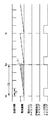
ここで、従来の撮像装置で行われるスローシャッターモードでの動画撮影処理について、図7のタイミングチャートを参照して説明する。 Here, the moving image shooting process in the slow shutter mode performed in the conventional imaging apparatus will be described with reference to the timing chart of FIG.
垂直同期信号は、周期T1でパルスを出力する信号であり、たとえばNTSC標準信号であれば1/60秒周期で繰り返しパルスを出力する。スローシャッターモードでは、電荷の蓄積は複数の垂直同期期間にまたがって行われ、図7に示す例では、t31からt32の4周期の間(T2の間)、撮像素子において電荷が蓄積される。71は、撮像素子において電荷が蓄積される様子を示している。蓄積された電荷は、t32に撮像素子から読み出される。このt32の読み出しタイミングから、次の動画像のための電荷蓄積が開始される。
The vertical synchronization signal is a signal that outputs a pulse at a cycle T1, and for example, an NTSC standard signal repeatedly outputs a pulse at a 1/60 second cycle. In the slow shutter mode, charges are accumulated over a plurality of vertical synchronization periods. In the example shown in FIG. 7, charges are accumulated in the image sensor during four periods from t 31 to t 32 (during T2). The
また、t32において、撮像素子から読み出された画像信号は記録されると共に、AF評価値の抽出が行われる。レンズ制御は、AF評価値の抽出後に行われる。 Further, in the t 32, the image signal read from the imaging element while being recorded, the extraction of the AF evaluation value is performed. The lens control is performed after the AF evaluation value is extracted.
このように、従来のスローシャッターモードでは、複数周期間、撮像素子を露光して得られた画像信号に基づいてレンズ制御を行うため、次の電荷蓄積が開始されるまで(図7の例ではt32まで)にレンズ制御を完了し、ピントを合わせることができなかった。このため、各露光時間T2において、その最初ではなく、途中に最もよく合焦した画像となっていた。 As described above, in the conventional slow shutter mode, lens control is performed based on the image signal obtained by exposing the imaging device for a plurality of periods, and therefore, until the next charge accumulation is started (in the example of FIG. 7). the lens control completed by t 32), it was not possible to focus. For this reason, at each exposure time T2, the image is best focused on the middle rather than the beginning.
また、特許文献1ではAF制御に関する記載が無い。
本発明は上記問題点を鑑みてなされたものであり、複数フレーム分またはフィールド分の画像信号を累計加算して、動画用の1枚分の画像信号を取得する場合に、各画像信号の露光時間の最初に最もよく合焦した画像を取得できるようにすることを第1の目的とする。 The present invention has been made in view of the above problems, and when image signals for a plurality of frames or fields are cumulatively added to obtain one image signal for a moving image, exposure of each image signal is performed. A first object is to obtain the best focused image at the beginning of time.
更に、複数フレーム分またはフィールド分の画像信号を累計加算して、動画用の1枚分の画像信号を取得する場合に、各画像信号の全体の露光時間の内、所望の時間に最もよく合焦した画像を取得できるようにすることを第2の目的とする。 Further, an image signal of a plurality of frames or fields fraction and cumulative addition, when obtaining an image signal for one sheet for video, of the total exposure time of each image signal, most often between when desired A second object is to make it possible to acquire a focused image.
上記第1の目的を達成するために、本発明の撮像装置は、入射する被写体光学像を光電変換して画像信号を出力する撮像素子と、予め設定された第1の周期で前記撮像素子が画像信号を出力するように制御する駆動制御手段と、前記第1の周期で前記撮像素子から出力される画像信号を順次累算して合成する合成手段と、前記第1の周期を整数倍した第2の周期で、前記合成手段により合成された画像信号を記録用として出力するとともに、前記第2の周期の途中で前記合成手段により合成された画像信号を焦点検出用として出力するように制御する制御手段と、前記第2の周期の途中から当該第2の周期の終了までの間に、前記焦点検出用の画像信号に基づいて、焦点調節処理を行う焦点調節手段とを有する。 In order to achieve the first object, an image pickup apparatus according to the present invention includes an image pickup device that photoelectrically converts an incident subject optical image and outputs an image signal, and the image pickup device at a preset first period. drive control means for controlling to output the image signals, and synthesizing means for synthesizing by accumulating an image signal output from the imaging device in the first period were sequentially integral multiple of the first cycle in the second period, the outputs of the disengaging made the image signal by the combining means for the recording, the second for the middle by the combining means focus detecting by Rigo made the image signal of the period And a focus adjustment unit that performs focus adjustment processing based on the image signal for focus detection between the middle of the second cycle and the end of the second cycle. And have.
また、入射する被写体光学像を光電変換して画像信号を出力する撮像素子を有する撮像装置の本発明の制御方法は、予め設定された第1の周期で前記撮像素子から画像信号を読み出す読み出し工程と、前記第1の周期で前記撮像素子から出力される画像信号を順次累算して合成する合成工程と、前記第1の周期を整数倍した第2の周期で、前記合成工程で合成された画像信号を記録用として出力する第1の出力工程と、前記第2の周期の途中で前記合成工程で累算合成された画像信号を焦点検出用として出力する第2の出力工程と、前記第2の周期の途中から当該第2の周期の終了までの間に、前記焦点検出用の画像信号に基づいて、焦点調節処理を行う焦点調節工程とを有する。 Further, the control method of the present invention of the image pickup apparatus having the image pickup device that photoelectrically converts the incident subject optical image and outputs the image signal reads out the image signal from the image pickup device at a preset first cycle. When a synthesizing step of synthesizing by accumulating an image signal output from the imaging device in the first period sequentially in a second period after the integral multiple of the first cycle, synthesis at the synthesis step A first output step for outputting the image signal for recording, a second output step for outputting the image signal accumulated and synthesized in the synthesis step in the middle of the second period for focus detection, A focus adjustment step of performing a focus adjustment process based on the image signal for focus detection between the middle of the second cycle and the end of the second cycle.
また、上記第2の目的を達成するために、本発明の撮像装置における前記制御手段は、前記第2の周期と周期が等しく、且つ、所望の時間に合成された画像信号が出力されるように前記第1の周期の整数倍位相を異ならせた第3の周期で、前記焦点検出用の画像信号を出力する。 Further, in order to achieve the second object, said control means in the imaging apparatus of the present invention, before SL equal second period and the period, and the image signal synthesized in the desired time is output in the third period and the different et allowed integral multiple phase of the first cycle as, you Outputs an image signal for the focus detection.
本発明によれば、複数フレーム分またはフィールド分の画像信号を累計加算して、動画用の1枚分の画像信号を取得する場合に、各画像信号の露光時間の最初に最もよく合焦した画像を取得することが可能となる。 According to the present invention, when the image signals for a plurality of frames or fields are cumulatively added to obtain one image signal for a moving image, the best focus is obtained at the beginning of the exposure time of each image signal. Images can be acquired.
また、複数フレーム分またはフィールド分の画像信号を累計加算して、動画用の1枚分の画像信号を取得する場合に、各画像信号の全体の露光時間の内、所望の時間に最もよく合焦した画像を取得することが可能となる。 Further, an image signal of a plurality of frames or fields fraction and cumulative addition, when obtaining an image signal for one sheet for video, of the total exposure time of each image signal, best if the desired time It is possible to acquire a focused image.
以下、添付図面を参照して本発明を実施するための最良の形態を詳細に説明する。 The best mode for carrying out the present invention will be described below in detail with reference to the accompanying drawings.
<第1の実施形態>
図1は、本発明の第1の実施形態におけるビデオカメラの概略構成を示すブロック図である。
<First Embodiment>
FIG. 1 is a block diagram showing a schematic configuration of a video camera according to the first embodiment of the present invention.
図1において、101は光学系の一部を構成するビデオカメラに着脱可能なレンズユニットであり、単一または複数のレンズからなるレンズ群を含む。レンズユニット101を透過した光は撮像素子102に入射し、電気信号に変換される。撮像素子102は、CCDセンサやCMOSセンサなどに代表されるイメージセンサであり、タイミングジェネレータ111から入力される駆動制御信号に基づいて所定の時間露光され、受光量に応じた電気信号(以下、「画像信号」と呼ぶ。)を出力する。タイミングジェネレータ111はタイミング制御回路108及び画像累積カウンタ109からなる制御部110によって制御され、タイミング制御回路108が出力する制御信号に従って、駆動制御信号を出力する。また、画像累積カウンタ109もタイミング制御回路108から出力される制御信号によって制御され、タイミングジェネレータ111によって駆動される撮像素子102の画像信号の読み出しタイミングと同期をとることで、撮影回数をカウントする。
In FIG. 1,
画像合成回路103は撮像素子102で変換された画像信号の累算処理を行って画像を合成する回路であり、合成された画像信号はセレクタ105を経由してフレームメモリ104へ記録されるか、またはカメラ信号処理回路107に出力される。セレクタ105は画像累積カウンタ109のカウント数に従って、画像合成回路103の出力先を、フレームメモリ104とカメラ信号処理回路107のいずれかに切り替える。カメラ信号処理回路107は画像合成回路103を介してにより合成された画像信号に対して所定の処理を行って画像データに変換し、不図示の記録回路や表示装置などに出力する。106はフレームメモリ104に記録されている画像信号を用いてAF評価値を検出するAF評価値検出回路であり、画像累積カウンタ109が所定の撮影回数をカウントしたタイミングでAF評価値の検出を行う。AF評価値検出回路106は、得られたAF評価値に基いてレンズユニット101の制御量を決定し、レンズ制御回路112へ出力する。レンズ制御回路112はAF評価値検出回路106の決定した制御量に基づいてレンズユニット101を駆動することで、被写体に合焦するように制御する。
The
続いて、上記構成を有するビデオカメラで、暗い被写体を撮影する際に行われる撮影処理について、図2のタイミングチャートを参照して説明する。 Next, shooting processing performed when shooting a dark subject with the video camera having the above configuration will be described with reference to a timing chart of FIG.
垂直同期信号は、周期T1でパルスを出力する信号であり、たとえばNTSC標準信号であれば1/60秒周期で繰り返しパルスを出力する。 The vertical synchronization signal is a signal that outputs a pulse at a cycle T1, and for example, an NTSC standard signal repeatedly outputs a pulse at a 1/60 second cycle.
「電荷蓄積」は、撮像素子102において電荷が蓄積される様子を示している。本第1の実施形態では、1垂直周期T1(1/60秒)毎に撮像素子102における電荷の蓄積及び画像信号の読み出しを行う。従って、蓄積された電荷11〜14はタイミングジェネレータ111から入力される駆動制御信号によって、垂直同期信号に同期した読み出しタイミングt12、t13、t14、t15で撮像素子102から読み出される。本第1の実施形態においては、周期T1で読み出される画像信号(以下、電荷11〜14に対応する画像信号にも同じ参照番号を用いる。)を4回累算処理することで、周期T2に1枚の動画用の画像データを生成するものとする。この場合、セレクタ105は、画像累積カウンタ109から出力されるカウントが撮影回数1〜3回を示す場合には、フレームメモリ104を選択し、4回目の時にカメラ信号処理回路107を選択するように動作する。
“Charge accumulation” indicates a state in which charges are accumulated in the
t11から蓄積され、t12で撮像素子102から読み出された画像信号11は画像合成回路103へ入力されるが、この画像信号11は合成する際の1枚目の画像であるため、累算処理はせずにフレームメモリ104に記録される。次に、t12から蓄積され、t13で読み出された画像信号12は画像合成回路103へ入力され、フレームメモリ104に記録されている画像信号11と累算処理により合成され、再びフレームメモリ104に記録される。
The
次に、t13から蓄積され、t14で読み出された画像信号13が画像合成回路103へ入力され、フレームメモリ104に記録されている画像信号11+12と累算処理され、再びフレームメモリ104に記録される。このようにして周期T2内で読み出された3回分の画像信号が累算処理によりフレームメモリ104に記録されることになる。この状態では、撮像素子102からの読み出し回数をカウントする画像累積カウンタ109は、撮影回数3回目のカウントを示している。画像信号13まで累算処理され、フレームメモリ104に記録された時点で、AF評価値検出回路106へ3回目の撮影であることを評価値抽出タイミングとしてAF評価値検出回路106へ伝える。AF評価値検出回路106は、t14において、評価値抽出タイミングに従ってフレームメモリ104に記録されている画像信号11+12+13からAF評価値を検出する。更に、レンズ制御タイミングでAF評価値を基にレンズユニット101の制御量を求め、レンズ制御回路112へ出力する。レンズ制御回路112はこの制御量を基に、レンズユニット101の制御を行い、被写体に合焦するようにピントを調整する。ここまでの処理をt14〜t15の間、すなわち4枚目の画像を露光している時間内に行う。
Next, the
また、t14から蓄積され、t15で読み出された画像信号14は画像合成回路103において、フレームメモリ104に記録されている画像信号11+12+13と累算処理される。ここで、撮像素子102からの読み出し回数をカウントする画像累積カウンタ109は撮影回数4回目を示しており、セレクタ105へ4回目の撮影であることを合成出力タイミングとして出力する。セレクタ105はこの合成出力タイミングに応じて画像合成回路103の出力先をカメラ信号処理回路107へ切り替える。これにより、画像信号11〜14を累算処理した合成出力16をフレームメモリ104に記録することなく、カメラ信号処理回路107へ出力する。
Further, the
次に、本第1の実施形態のビデオカメラにおける、撮像素子102からの画像信号の読み出しからカメラ信号処理回路107への出力までの動作について、図3のフローチャートを参照して説明する。なお、このフローチャートは図2のタイミングチャートと同様に、撮像素子102から読み出される画像信号を4回累算処理することで1枚の動画用の画像信号を生成するものとする。
Next, the operation from the reading of the image signal from the
不図示の撮影ボタンなどの操作により撮影が指示されると、撮影処理が開始される。まず、ステップS11において、制御部110は、画像累積カウンタの値、つまり、画像信号の読み出し回数Nを0にリセットする。次に、ステップS12において画像信号の読み出し回数Nを1増やし、ステップS13に進んで、撮像素子102から画像信号の読み出しを行う。ステップS14ではフレームメモリ104に記録されている画像信号と撮像素子102から読み出した画像信号の累積処理をする。ステップS15において、読み出し回数Nが4であるかどうか判断する。ここで、読み出し回数Nが4である場合は累算処理された合成出力の出力タイミングであると判断し、ステップS16へ進む。一方、読み出し回数Nが4でない場合は、合成出力の出力タイミングでないと判断しステップS18へ進む。
When shooting is instructed by operating a shooting button (not shown), shooting processing is started. First, in step S11, the control unit 110 resets the value of the image accumulation counter, that is, the number N of image signal readouts, to zero. Next, in step S <b> 12, the number N of image signal readouts is increased by 1, and the process proceeds to step S <b> 13 to read out image signals from the
ステップS18では、累算処理された画像信号をフレームメモリ104へ記録し、ステップS19において、読み出し回数Nが3であるかどうか判断する。読み出し回数Nが3である場合はAF評価値の取得タイミングであると判断してステップS20へ進む。一方、読み出し回数Nが3でない場合は、AF評価値取得のタイミングではないと判断し、ステップS12へ戻る。
In step S18, the accumulated image signal is recorded in the
ステップS20では、フレームメモリ104に記録されている画像信号からAF評価値を取得し、ステップS21において、得られたAF評価値からレンズ制御量を決定し、レンズ制御回路112がレンズユニット101の制御を開始する。
In step S20, an AF evaluation value is acquired from the image signal recorded in the
一方、ステップS15において読み出し回数Nが4であると判断した場合、ステップS16では、累算処理された画像信号をカメラ信号処理回路107へ出力する。ステップS17では、撮影が終了したかどうかを判断する。ここで撮影が終了であると判断された場合には、処理を終了する。一方、撮影が終了していないと判断されたときはステップS11へ戻る。
On the other hand, when it is determined in step S15 that the number N of readings is 4, in step S16, the accumulated image signal is output to the camera
上記の通り本第1の実施形態によれば、AF制御用の画像は3枚分の画像信号を基に行うため、4枚目の画像信号を蓄積している間に合焦制御を行うことが可能となる。これにより、累算して得られた動画用の各画像において、露光時間の最初に最もよく合焦した画像を取得することができる。 As described above, according to the first embodiment, since the AF control image is based on the image signals for three images, focus control is performed while the fourth image signal is being accumulated. Is possible. Thereby, in each image for moving images obtained by accumulation, it is possible to acquire an image that is best focused at the beginning of the exposure time.
なお、上記第1の実施形態では、各垂直期間で得られた4枚分の画像信号を累算処理して1枚の画像を取得する場合について説明したが、本発明において累算する画像の枚数は4枚に限るものではなく、被写体の明るさに応じて適宜変更することができる。また、AF評価値を検出するタイミングとして、3枚分の画像を累算処理した時としたが、これも3枚に限るものでは無く、累算処理により合成される次の画像の撮影開始前にレンズ制御が終了するタイミングであればよい。 In the first embodiment, the case has been described where four image signals obtained in each vertical period are accumulated and one image is acquired. The number of sheets is not limited to four, and can be appropriately changed according to the brightness of the subject. Further, although the timing for detecting the AF evaluation value is the time when the image for three images is accumulated, this is not limited to three, but before the start of the next image to be synthesized by the accumulation processing. Any timing may be used as long as the lens control ends.
上記説明では、図1に示すビデオカメラの構成において、画像信号の累積処理を行う場合(つまり、被写体が暗い場合)について説明した。これに対し、被写体が十分に明るい場合には累積処理を行う必要がないため、画像累積カウンタ109は各垂直期間に同期してAF用画像合成タイミング信号と、記録画像合成タイミング信号を出力する。これにより、セレクタ105は常にカメラ信号処理回路107を選択し、AF評価値検出回路106は、各垂直期間毎にAF評価値を算出し、レンズユニット101が制御されることになる。なお、この場合、不図示ではあるが、AF評価値検出回路106はフレームメモリ104を介さずに、撮像素子102または画像合成回路103を介して、画像信号を取得する。
In the above description, the case where the image signal accumulation processing is performed in the configuration of the video camera shown in FIG. 1 (that is, the subject is dark) has been described. On the other hand, when the subject is sufficiently bright, it is not necessary to perform accumulation processing, so the
<第2の実施形態>
次に、本発明の第2の実施形態について説明する。
<Second Embodiment>
Next, a second embodiment of the present invention will be described.
図4は、本発明の第2の実施形態におけるビデオカメラの概略構成を示すブロック図である。図4において、図1と同様の構成には同じ参照番号を付している。 FIG. 4 is a block diagram showing a schematic configuration of a video camera according to the second embodiment of the present invention. In FIG. 4, the same reference numerals are given to the same components as those in FIG.
図4において、101は光学系の一部を構成するビデオカメラに着脱可能なレンズユニットであり、単一または複数のレンズからなるレンズ群を含む。レンズユニット101を透過した光は撮像素子102に入射し、電気信号に変換される。撮像素子102は、CCDセンサやCMOSセンサなどに代表されるイメージセンサであり、タイミングジェネレータ111から入力される駆動制御信号に基づいて所定の時間露光され、受光量に応じた電気信号(画像信号)を出力する。タイミングジェネレータ111はタイミング制御回路108及び画像合成タイミング切替器404からなるタイミング制御部405によって制御され、タイミング制御回路108が出力する制御信号に従って、駆動制御信号を出力する。また、画像合成タイミング切替器404もタイミング制御回路108から出力される制御信号によって制御され、タイミングジェネレータ111によって駆動される撮像素子102の画像信号の読み出し回数と同期をとることで画像合成のタイミングを出力する。
In FIG. 4,
撮像素子102から読み出された画像信号はフレームメモリ104に逐次記録される。403は記録画像合成回路401及びAF画像合成回路402から成る画像合成部で、フレームメモリ104から記録されている画像データの読み出しを行い、記録画像合成回路401とAF画像合成回路402それぞれにおいて画像データの累算処理を行う。記録画像合成回路401とAF画像合成回路402は、それぞれ画像合成タイミング切替器404から出力される後述するタイミングに従って、累算処理した画像データを出力する。
Image signals read from the
AF評価値検出回路106はAF画像合成回路402において累算処理された画像データからAF評価値を検出し、更に、得られたAF評価値に基づいてレンズユニット101の制御量を決定し、レンズ制御回路112へ出力する。レンズ制御回路112はAF評価値検出回路106が決定した制御量に基づいてレンズユニット101を駆動することで、被写体に合焦するように制御する。
The AF evaluation
カメラ信号処理回路107は、画像合成タイミング切替器404が出力する制御信号に基づくタイミングで記録画像合成回路401から出力された画像データに対して、所定の画像処理を行って画像データに変換し、不図示の記録回路や表示装置などに出力する。
The camera
続いて、上記構成を有するビデオカメラで、暗い被写体を撮影する際に行われる撮影処理について、図5のタイミングチャートを参照して説明する。 Next, shooting processing performed when shooting a dark subject with the video camera having the above configuration will be described with reference to a timing chart of FIG.
垂直同期信号は周期T1でパルスを出力する信号であり、たとえばNTSC標準信号であれば1/60秒周期で繰り返しパルスを出力する。 The vertical synchronization signal is a signal that outputs a pulse at a cycle T1, and for example, an NTSC standard signal repeatedly outputs a pulse at a 1/60 second cycle.
「電荷蓄積」は、撮像素子102において電荷が蓄積される様子を示している。第1の実施形態と同様に、本第2の実施形態においても、1垂直周期T1(1/60秒)毎に撮像素子102における電荷の蓄積及び画像信号の読み出しを行う。従って、蓄積された電荷21〜26はタイミングジェネレータ111から入力される駆動制御信号によって、垂直同期信号に同期した読み出しタイミングt21、t22、t23、t24、t25、t26で撮像素子102から読み出される。本第2の実施形態においては、垂直同期信号の周期T2で読み出される画像信号(以下、電荷21〜26に対応する画像信号にも同じ参照番号を用いる。)を4回累算処理することで、周期T2に1枚の動画用の画像データを生成するものとする。
“Charge accumulation” indicates a state in which charges are accumulated in the
T1の間蓄積され、t21で撮像素子102から読み出された画像信号21は、逐次フレームメモリ101に記録されていく。AF画像合成回路401はt21で画像合成タイミング切替器404から出力されるAF用画像合成タイミングに従って、画像信号の累算処理を開始する。そして、t22、t23、t24、t25それぞれのタイミングで読み出された画像信号22〜25を累算処理する。t25では、それまで累算処理した画像信号22+23+24+25からAF評価値を検出し、検出したAF評価値を基にレンズユニット101の制御量を決定し、レンズ制御回路112へ出力する。レンズ制御回路112はこの制御量を基にレンズユニット101の制御を行い、被写体に合焦するようにピントを調整する。ここまでの処理をt24〜t25の間、からすなわち撮影時間T2内で4枚目の画像を露光している時間内に行う。
Accumulated during T1, the
また、記録画像合成回路401は、t22で画像合成タイミング切替器404から出力される記録画像合成タイミング信号に従ってフレームメモリ104から画像データの読み出しを行い、画像データの累算処理を開始する。そして、t23、t24、t25、t26それぞれのタイミングで読み出された画像信号23〜26を累算処理する。t26では、それまで累算処理した画像信号23+24+25+26をカメラ信号処理回路107に出力する。
Further, the recorded
図5のタイミングチャートから分かるように、AF評価値検出用の画像はタイミングt21からt25の時間T3で累算処理するのに対し、記録用の画像はt22からt26の時間T4で累算処理して得られる。 As can be seen from the timing chart of FIG. 5, while the image for detecting the AF evaluation value is accumulated processing time T3 of t 25 from the timing t 21, the image for recording in the time T4 of t 26 from t 22 Obtained by accumulating.
次に、本第2の実施形態のビデオカメラにおける、撮像素子102からの画像信号の読み出しからカメラ信号処理回路107への出力までの動作について、図6のフローチャートを参照して説明する。なお、このフローチャートは図5のタイミングチャートと同様に、撮像素子102から読み出される画像信号を4回累算処理することで1枚の動画用の画像信号を生成するものとする。
Next, the operation from the reading of the image signal from the
不図示の撮影ボタンなどの操作により撮影が指示されると、撮影処理が開始される。まず、ステップS31において、撮像素子102から画像信号の読み出しを行い、ステップS32で読み出した画像信号をフレームメモリ104に記憶する。次に、ステップS33においてAF画像合成回路402はフレームメモリ104から画像データを読み出し累算処理を行うと共に、ステップS34において記録画像合成回路401もフレームメモリ104から画像信号を読み出して累算処理を行う。
When shooting is instructed by operating a shooting button (not shown), shooting processing is started. First, in step S31, an image signal is read from the
ステップS35において、AF評価値検出タイミングがONになったかどうかを判断する。ここで、AF評価値検出タイミングがONである場合、ステップS36に進んでAF画像合成回路402で累算された画像信号からAF評価値の検出を行い、ステップS37で検出されたAF評価値からレンズ制御量を決定し、レンズ制御回路112がレンズユニット101の制御を開始する。レンズユニット101の制御が終わると、ステップS38に進む。
In step S35, it is determined whether or not the AF evaluation value detection timing is ON. If the AF evaluation value detection timing is ON, the process proceeds to step S36 to detect the AF evaluation value from the image signal accumulated by the AF
また、ステップS35においてAF評価値検出タイミングがONでない場合は、直接ステップS38へ進む。 If the AF evaluation value detection timing is not ON in step S35, the process proceeds directly to step S38.
ステップS38において、記録画像出力タイミングがONになったかどうかを判断する。ここで、記録画像出力タイミングがONである場合、ステップS39へ進む。一方、記録画像出力タイミングがONでない場合は、合成画像の出力のタイミングでないと判断し、ステップS31に戻って、上記制御を繰り返す。 In step S38, it is determined whether the recording image output timing has been turned ON. If the recording image output timing is ON, the process proceeds to step S39. On the other hand, if the recording image output timing is not ON, it is determined that it is not the timing for outputting the composite image, and the process returns to step S31 to repeat the above control.
ステップS39では、累算処理された画像信号をカメラ信号処理回路107へ出力する。次のステップS40において撮影が終了したかどうかを判断し、撮影が終了していないと判断されたときはステップS31に戻って上記処理を繰り返し、撮影が終了であると判断されると、撮影処理を終了する。
In step S 39, the accumulated image signal is output to the camera
上記の通り本第2の実施形態によれば、AF制御用の画像と記録用の画像とで累算処理する画像をシフトすることにより、記録用画像の4枚目の画像信号を蓄積している間に合焦制御を行うことが可能となる。これにより、累算して得られた動画用の各画像において、露光時間の最初に最もよく合焦した画像を取得することができる。 As described above, according to the second embodiment, the fourth image signal of the recording image is accumulated by shifting the image to be accumulated between the AF control image and the recording image. In-focus control can be performed during the time. Thereby, in each image for moving images obtained by accumulation, it is possible to acquire an image that is best focused at the beginning of the exposure time.
なお、上記第2の実施形態では、1垂直期間分、AF制御用の画像の累算処理を記録用の画像の累積処理に比べて先にシフトするようにしたが、本発明はこれに限るものではない。累算して得られる動画用の各画像について、各画像の全体の露光時間の内、所望の時間に最もよく合焦した画像を取得できるようにシフト量を変更することも可能である。 In the second embodiment, the accumulation process of the AF control image is shifted earlier than the accumulation process of the recording image for one vertical period. However, the present invention is not limited to this. It is not a thing. With respect to each moving image obtained by accumulation, it is possible to change the shift amount so as to obtain an image that is best focused on a desired time within the entire exposure time of each image .
また、上記第2の実施形態では、各垂直期間で得られた4枚分の画像信号を累算処理して1枚の画像を取得する場合について説明したが、本発明において累算する画像の枚数は4枚に限るものではなく、被写体の明るさに応じて適宜変更することができる。 In the second embodiment, the case where four image signals obtained in each vertical period are accumulated to obtain one image has been described. The number of sheets is not limited to four, and can be appropriately changed according to the brightness of the subject.
上記説明では、図4に示すビデオカメラの構成において、画像信号の累積処理を行う場合(つまり、被写体が暗い場合)について説明した。これに対し、被写体が十分に明るい場合には累積処理を行う必要がないため、画像合成タイミング切換替器404は、垂直期間毎に垂直同期信号に同期して記録画像合成回路401及びAF画像合成回路402に制御信号を出力する。なお、制御信号とは、AF用画像合成タイミング信号、記録画像合成タイミング信号、評価値検出タイミング信号、記録画像出力タイミング信号である。これにより、記録画像合成回路401及びAF画像合成回路は、フレームメモリ104から読み出した画像信号を、垂直期間毎にカメラ信号処理回路107及びAF評価値検出回路106にそれぞれ出力する。
In the above description, the case where the image signal accumulation process is performed in the configuration of the video camera shown in FIG. 4 (that is, the subject is dark) has been described. On the other hand, when the subject is sufficiently bright, there is no need to perform accumulation processing. Therefore, the image composition
101 レンズ
102 撮像素子
103 画像合成回路
104 フレームメモリ
105 セレクタ
106 AF評価値検出回路
107 カメラ信号処理回路
108 タイミング制御回路
109 画像累積カウンタ
110 制御部
111 タイミングジェネレータ
112 レンズ制御回路
401 記録画像合成回路
402 AF画像合成回路
403 画像合成部
404 画像合成タイミング切替器
405 タイミング制御部
DESCRIPTION OF
Claims (4)
予め設定された第1の周期で前記撮像素子が画像信号を出力するように制御する駆動制御手段と、
前記第1の周期で前記撮像素子から出力される画像信号を順次累算して合成する合成手段と、
前記第1の周期を整数倍した第2の周期で、前記合成手段により合成された画像信号を記録用として出力するとともに、前記第2の周期の途中で前記合成手段により合成された画像信号を焦点検出用として出力するように制御する制御手段と、
前記第2の周期の途中から当該第2の周期の終了までの間に、前記焦点検出用の画像信号に基づいて、焦点調節処理を行う焦点調節手段と
を有することを特徴とする撮像装置。 An image sensor that photoelectrically converts an incident subject optical image and outputs an image signal;
Drive control means for controlling the image sensor to output an image signal at a preset first period;
Synthesizing means for sequentially accumulating and synthesizing image signals output from the image sensor in the first period;
The image signal synthesized by the synthesizing unit is output for recording in a second cycle obtained by multiplying the first cycle by an integer, and the image signal synthesized by the synthesizing unit in the middle of the second cycle is output. Control means for controlling to output for focus detection;
An image pickup apparatus comprising: a focus adjustment unit that performs a focus adjustment process based on the image signal for focus detection between the middle of the second cycle and the end of the second cycle.
前記制御手段は、前記第1の画像合成手段を前記第2の周期で制御し、前記第2の画像合成手段を前記第3の周期で制御することを特徴とする請求項2に記載の撮像装置。 The synthesizing unit includes a first image synthesizing unit and a second image synthesizing unit,
3. The imaging according to claim 2, wherein the control unit controls the first image synthesizing unit in the second cycle, and controls the second image synthesizing unit in the third cycle. apparatus.
予め設定された第1の周期で前記撮像素子から画像信号を読み出す読み出し工程と、
前記第1の周期で前記撮像素子から出力される画像信号を順次累算して合成する合成工程と、
前記第1の周期を整数倍した第2の周期で、前記合成工程で合成された画像信号を記録用として出力する第1の出力工程と、
前記第2の周期の途中で前記合成工程で合成された画像信号を焦点検出用として出力する第2の出力工程と、
前記第2の周期の途中から当該第2の周期の終了までの間に、前記焦点検出用の画像信号に基づいて、焦点調節処理を行う焦点調節工程と
を有することを特徴とする制御方法。 A method for controlling an image pickup apparatus having an image pickup device that photoelectrically converts an incident subject optical image and outputs an image signal,
A reading step of reading out an image signal from the image sensor at a preset first period;
A synthesis step of sequentially accumulating and synthesizing image signals output from the image sensor in the first period;
A first output step of outputting the image signal synthesized in the synthesis step for recording in a second cycle obtained by multiplying the first cycle by an integer;
A second output step of outputting the image signal synthesized in the synthesis step in the middle of the second period for focus detection;
A focus adjustment step of performing a focus adjustment process on the basis of the image signal for focus detection between the middle of the second cycle and the end of the second cycle.
Priority Applications (1)
| Application Number | Priority Date | Filing Date | Title |
|---|---|---|---|
| JP2006095845A JP4827577B2 (en) | 2006-03-30 | 2006-03-30 | Imaging apparatus and control method |
Applications Claiming Priority (1)
| Application Number | Priority Date | Filing Date | Title |
|---|---|---|---|
| JP2006095845A JP4827577B2 (en) | 2006-03-30 | 2006-03-30 | Imaging apparatus and control method |
Publications (3)
| Publication Number | Publication Date |
|---|---|
| JP2007274211A JP2007274211A (en) | 2007-10-18 |
| JP2007274211A5 JP2007274211A5 (en) | 2009-05-14 |
| JP4827577B2 true JP4827577B2 (en) | 2011-11-30 |
Family
ID=38676569
Family Applications (1)
| Application Number | Title | Priority Date | Filing Date |
|---|---|---|---|
| JP2006095845A Expired - Fee Related JP4827577B2 (en) | 2006-03-30 | 2006-03-30 | Imaging apparatus and control method |
Country Status (1)
| Country | Link |
|---|---|
| JP (1) | JP4827577B2 (en) |
Families Citing this family (2)
| Publication number | Priority date | Publication date | Assignee | Title |
|---|---|---|---|---|
| JP5820720B2 (en) * | 2011-12-27 | 2015-11-24 | オリンパス株式会社 | Imaging device |
| JP5829122B2 (en) * | 2011-12-27 | 2015-12-09 | オリンパス株式会社 | Imaging apparatus and evaluation value generation apparatus |
Family Cites Families (1)
| Publication number | Priority date | Publication date | Assignee | Title |
|---|---|---|---|---|
| JPH0795841B2 (en) * | 1992-04-21 | 1995-10-11 | オリンパス光学工業株式会社 | Image recorder |
-
2006
- 2006-03-30 JP JP2006095845A patent/JP4827577B2/en not_active Expired - Fee Related
Also Published As
| Publication number | Publication date |
|---|---|
| JP2007274211A (en) | 2007-10-18 |
Similar Documents
| Publication | Publication Date | Title |
|---|---|---|
| KR101605419B1 (en) | Photographing apparatus and method of photographing | |
| JP5447619B2 (en) | Imaging device | |
| JP2006222935A (en) | Electronic still camera, image capturing method, program and storage medium | |
| JP2019054461A (en) | Imaging apparatus and imaging method | |
| JP2011155396A (en) | Image capture apparatus | |
| JP2011135185A (en) | Imaging device | |
| JP2006261929A (en) | Image pickup device | |
| JP2010166304A (en) | Photographing apparatus, method of controlling the same, and program | |
| JP2020012879A (en) | Imaging element, focus detection device, imaging method, and focus detection method | |
| JP4827577B2 (en) | Imaging apparatus and control method | |
| JP2012119788A (en) | Imaging device, image processing device, imaging method and image processing method | |
| JP4187512B2 (en) | Imaging device | |
| JP5273895B2 (en) | Imaging device and lens device | |
| JP5354879B2 (en) | camera | |
| JP5947625B2 (en) | Imaging apparatus and control method thereof | |
| JP2010107662A (en) | Imaging apparatus, range-finding device and range-finding method | |
| JP2002135646A (en) | Imaging unit, method for imaging and storage medium | |
| JP2006165725A (en) | Imaging apparatus and its exposure determination method | |
| JP2011019062A (en) | Imaging device, image selection method, and program | |
| JP2021004989A (en) | Focus adjustment device and focus adjustment method | |
| JP2002152602A (en) | Digital still camera | |
| JP5022802B2 (en) | Imaging apparatus and control method thereof | |
| JP2013251877A (en) | Imaging apparatus | |
| WO2022255318A1 (en) | Imaging device and image processing device | |
| JP6929752B2 (en) | Focus detection device and focus detection method |
Legal Events
| Date | Code | Title | Description |
|---|---|---|---|
| A521 | Request for written amendment filed |
Free format text: JAPANESE INTERMEDIATE CODE: A523 Effective date: 20090327 |
|
| A621 | Written request for application examination |
Free format text: JAPANESE INTERMEDIATE CODE: A621 Effective date: 20090327 |
|
| A977 | Report on retrieval |
Free format text: JAPANESE INTERMEDIATE CODE: A971007 Effective date: 20101217 |
|
| A131 | Notification of reasons for refusal |
Free format text: JAPANESE INTERMEDIATE CODE: A131 Effective date: 20110207 |
|
| A521 | Request for written amendment filed |
Free format text: JAPANESE INTERMEDIATE CODE: A523 Effective date: 20110404 |
|
| TRDD | Decision of grant or rejection written | ||
| A01 | Written decision to grant a patent or to grant a registration (utility model) |
Free format text: JAPANESE INTERMEDIATE CODE: A01 Effective date: 20110909 |
|
| A01 | Written decision to grant a patent or to grant a registration (utility model) |
Free format text: JAPANESE INTERMEDIATE CODE: A01 |
|
| A61 | First payment of annual fees (during grant procedure) |
Free format text: JAPANESE INTERMEDIATE CODE: A61 Effective date: 20110913 |
|
| FPAY | Renewal fee payment (event date is renewal date of database) |
Free format text: PAYMENT UNTIL: 20140922 Year of fee payment: 3 |
|
| FPAY | Renewal fee payment (event date is renewal date of database) |
Free format text: PAYMENT UNTIL: 20140922 Year of fee payment: 3 |
|
| LAPS | Cancellation because of no payment of annual fees |