JP4815051B2 - Low switching magnetic tunnel junction - Google Patents
Low switching magnetic tunnel junction Download PDFInfo
- Publication number
- JP4815051B2 JP4815051B2 JP2000560586A JP2000560586A JP4815051B2 JP 4815051 B2 JP4815051 B2 JP 4815051B2 JP 2000560586 A JP2000560586 A JP 2000560586A JP 2000560586 A JP2000560586 A JP 2000560586A JP 4815051 B2 JP4815051 B2 JP 4815051B2
- Authority
- JP
- Japan
- Prior art keywords
- magnetic
- layer
- vector
- tunnel junction
- parallel
- Prior art date
- Legal status (The legal status is an assumption and is not a legal conclusion. Google has not performed a legal analysis and makes no representation as to the accuracy of the status listed.)
- Expired - Lifetime
Links
Images


Classifications
-
- G—PHYSICS
- G11—INFORMATION STORAGE
- G11C—STATIC STORES
- G11C11/00—Digital stores characterised by the use of particular electric or magnetic storage elements; Storage elements therefor
- G11C11/02—Digital stores characterised by the use of particular electric or magnetic storage elements; Storage elements therefor using magnetic elements
- G11C11/16—Digital stores characterised by the use of particular electric or magnetic storage elements; Storage elements therefor using magnetic elements using elements in which the storage effect is based on magnetic spin effect
- G11C11/161—Digital stores characterised by the use of particular electric or magnetic storage elements; Storage elements therefor using magnetic elements using elements in which the storage effect is based on magnetic spin effect details concerning the memory cell structure, e.g. the layers of the ferromagnetic memory cell
-
- G—PHYSICS
- G11—INFORMATION STORAGE
- G11C—STATIC STORES
- G11C11/00—Digital stores characterised by the use of particular electric or magnetic storage elements; Storage elements therefor
- G11C11/02—Digital stores characterised by the use of particular electric or magnetic storage elements; Storage elements therefor using magnetic elements
- G11C11/16—Digital stores characterised by the use of particular electric or magnetic storage elements; Storage elements therefor using magnetic elements using elements in which the storage effect is based on magnetic spin effect
- G11C11/165—Auxiliary circuits
- G11C11/1675—Writing or programming circuits or methods
-
- G—PHYSICS
- G11—INFORMATION STORAGE
- G11C—STATIC STORES
- G11C11/00—Digital stores characterised by the use of particular electric or magnetic storage elements; Storage elements therefor
- G11C11/56—Digital stores characterised by the use of particular electric or magnetic storage elements; Storage elements therefor using storage elements with more than two stable states represented by steps, e.g. of voltage, current, phase, frequency
- G11C11/5607—Digital stores characterised by the use of particular electric or magnetic storage elements; Storage elements therefor using storage elements with more than two stable states represented by steps, e.g. of voltage, current, phase, frequency using magnetic storage elements
-
- H—ELECTRICITY
- H10—SEMICONDUCTOR DEVICES; ELECTRIC SOLID-STATE DEVICES NOT OTHERWISE PROVIDED FOR
- H10B—ELECTRONIC MEMORY DEVICES
- H10B61/00—Magnetic memory devices, e.g. magnetoresistive RAM [MRAM] devices
-
- H—ELECTRICITY
- H10—SEMICONDUCTOR DEVICES; ELECTRIC SOLID-STATE DEVICES NOT OTHERWISE PROVIDED FOR
- H10N—ELECTRIC SOLID-STATE DEVICES NOT OTHERWISE PROVIDED FOR
- H10N50/00—Galvanomagnetic devices
- H10N50/10—Magnetoresistive devices
-
- G—PHYSICS
- G11—INFORMATION STORAGE
- G11C—STATIC STORES
- G11C2211/00—Indexing scheme relating to digital stores characterized by the use of particular electric or magnetic storage elements; Storage elements therefor
- G11C2211/56—Indexing scheme relating to G11C11/56 and sub-groups for features not covered by these groups
- G11C2211/561—Multilevel memory cell aspects
- G11C2211/5615—Multilevel magnetic memory cell using non-magnetic non-conducting interlayer, e.g. MTJ
Landscapes
- Engineering & Computer Science (AREA)
- Computer Hardware Design (AREA)
- Hall/Mr Elements (AREA)
- Semiconductor Memories (AREA)
- Mram Or Spin Memory Techniques (AREA)
Description
(技術分野)
本発明は、一般にメモリ・セルのための磁性トンネル接合部に関し、さらに詳しくは、きわめて高密度アレイのメモリ・セルのためのきわめて小型の磁性接合部に関する。
【0001】
(背景技術)
磁気ランダム・アクセス・メモリ(MRAM:magnetic random access memory)とは、大型抗磁性(GMR: giant magnetoresitive)材料または磁性トンネル接合部(MTJ: magnetic tunneling junction)構造,検知線およびワード線を基本的に具備する不揮発性メモリである。MRAMは、メモリ状態を格納するために磁気ベクトルを利用する。GMR材料またはMTJの1層または全層内の磁気ベクトルは、一定の閾値または強度を超えて磁界が磁気材料に印加されると、ある方向から他方向へときわめて迅速に切り替わる。GMR材料またはMTJ内の磁気ベクトルの方向に応じて状態が格納される。たとえば、一方向を論理「0」と定義し、他方向を論理「1」と定義することができる。GMR材料またはMTJは、磁界が印加されなくてもこれらの状態を維持する。GMR材料またはMTJ内に格納される状態は、2つの状態の抵抗の差により、検知線内のセルに検知電流を通過させることによって読み取ることができる。
【0002】
磁気メモリ・セルの非常に密度の高いアレイにおいては、アレイを現在の電子装置に利用できるだけ充分に小型に構築すると、個々のセルの寸法はきわめて小さくなる。個々のセルの寸法が小さくなるにつれて、アスペクト比(長さ/幅の比)が概して小さくなる。2層磁気メモリ・セルたとえば標準的なトンネル・セルにおいては、アスペクト比が5よりも小さくなると、セル内の磁気ベクトルは、非励起(ゼロ磁界)条件において逆平行になる。1996年9月25日に出願され同譲受人に譲渡された同時継続出願「Multi-Layer Magnetic Memory Cells with Improved Switching Characteristics」と題される第08/723,159号には、逆平行磁気ベクトルを伴うセルの読み取り方法が開示される。また1997年4月7日に出願され同譲受人に譲渡された同時継続出願「Magnetic Device Having Multi-Layers with Insulating and Conductive Layers」と題される第08/834,968号においては、2つの磁気層積層部にダミーの磁気層が追加されて2つの磁気層の一方に結合されて、他の磁気層が自由層になる。ダミーの磁気層を用いる方法の欠点は、2つの磁気層間の静磁気作用の打ち消しに依存し、この静磁気作用の強度はセルの幾何学的形状と層間の間隔とに依存することである。これらのパラメータは、臨界寸法が縮むと変わる。
【0003】
また、2層磁気メモリ・セル、たとえば標準的なトンネル・セルにおいては、アスペクト比が5よりも小さくなると、セルの状態を切り替えるために必要な磁界量が劇的に増大する。一般に、セルが小さくなると、セルの層はセルの状態を切り替えるために必要な磁界量を小さくするために、さらに薄くなるが、これは磁気モーメント(材料により決まる)に層の厚みを乗じた値が必要な切り替え磁界を決定するためである。磁気モーメントを小さくするためにより柔軟な磁気材料を用いることもできるが、超小型メモリ・セルについては、切り替え磁界の削減には限界がある。また、セルが小さくなると不安定になる。これは、たとえば、メモリ・セルの寸法が10nm以下の場合、セルの体積に比例する磁化のエネルギ・バリアが体積の減少に伴って減少し、熱変動エネルギすなわちKTに近づくためである。
【0004】
従って、より少ない磁界で書き込む(切替状態を格納する)ことができ、熱変動エネルギにより影響を受けない程の充分な体積を有する磁気ランダム・アクセス・メモリおよびメモリ・セルを提供することがきわめて望ましい。
【0005】
本発明の別の目的は、必要な切替磁界を削減するよう設計される強磁性結合磁気層を伴う新規の改善された多重状態多層磁気メモリ・セルを提供することである。
【0006】
本発明のさらに別の目的は、きわめて小型に、5未満のアスペクト比で作成することができる強磁性結合磁気層を伴う新規の改善された多重状態多層磁気メモリ・セルを提供することである。
【0007】
本発明のさらに別の目的は、磁化のエネルギ・バリアが増大された新規の改善された多重状態多層磁気メモリ・セルを提供することである。
【0008】
(産業上の利用可能性)
第1および第2抗磁層を有し、1対の抗磁層の間に平行に並置される非磁気導電層を有する反強磁性結合多層構造を備える低切替磁界抗磁性トンネル接合メモリ・セルにおいて、上記の問題および他の問題点が少なくとも部分的に解決され、上記の目的および他の目的が実現される。反強磁性結合多層構造における1対の抗磁層は、異なる厚みまたは異なる磁気材料を有することにより、異なる磁界において切り替わるように構築される。また、反強磁性結合多層構造における1対の抗磁層は、それぞれ、1対の層の反強磁性結合とアスペクト比とにより磁界が印加されない状態で逆平行になる磁気ベクトルを有する。セルは、第2抗磁層のベクトルに対して一定の関係を有する磁気ベクトルを有する抗磁構造をさらに備える。絶縁材料が反強磁性結合多層構造と抗磁構造との間に平行並置されて、磁性トンネル接合部を形成する。
【0009】
基本的には、セル内の状態を切り替えるのに必要とされる磁界は、反強磁性結合多層構造内の2つの抗磁層間の差により表される。また第1および第2構造はそれぞれ、正味の磁気モーメントをほとんど持たず、あるいは持たないように構築することができるので、メモリ・セルの正味の磁気モーメントはほとんどなく、隣接するセルに影響を与えずに隣接セルのより近くに配置することができる。
(実施例)
図1を参照して、図1は本発明による低切替磁界磁性トンネル接合メモリ・セル10の拡大された簡略側面図を示す。磁性トンネル接合部10は、一般に支持基板11上に形成され、基板11上に指示される抗磁構造12と、構造12上に配置される絶縁材料層13と、絶縁材料層13上に、層13を抗磁構造12,15間に挟み込んでトンネル接合部を形成するよう配置される抗磁構造15とを備える。
【0010】
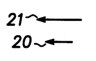
抗磁構造15は、抗磁層17,18の間に平行並置される非磁気導電層19を有する抗磁層17,18を備える反強磁性結合多層構造によって構成される。抗磁層17は、基板11の平面に平行な好適な磁気軸に沿う磁気ベクトル20を有し、抗磁層18は磁気ベクトル21を有する。磁気ベクトル20,21は、抗磁層17,18の間の反強磁性結合および/または約5未満のアスペクト比のために、磁性トンネル接合部10に磁界が印加されない場合に逆平行になる。一般に、約4未満の長さ/幅の比を有するセルにおいては、磁性材料の層(図1では層17,18)は反強磁性結合される。一般的に、この開示に関しては、「反強磁性結合」という用語は、逆平行状態(図1および図2に示される)のいずれか一方が安定であり、平行状態が不安定であって磁気ベクトルは常に逆平行状態に向かって移動する(反対方向を指す)ので、一定の磁界を必要とすることを意味する。抗磁構造15の構造,形状および寸法によっては、ベクトル20,21を形状または磁気結晶異方性により好適な磁気軸に沿うようにすることもできる。
【0011】
たとえば円形のセルの場合は、好適な磁化方向は、一軸結晶磁界異方性(または磁気結晶異方性)により決定することができる。この好適な磁化方向は、バイアス界または高温(たとえば摂氏200ないし300度)で高磁界(たとえば数kOe)において付着させた後で膜をアニーリングすることにより、膜付着中に設定される。正方形またはひし形の場合は、一軸結晶異方性は正方形の対角線方向に沿って設定することができる。楕円形または矩形のセルの場合は、一軸結晶異方性はセルの長軸に沿って設定することができる。ここで述べる好適な特徴は、狭いセル幅において必要な切替磁界を上げることに貢献する形状の影響を最小限に抑え、メモリ・セルが必要とする好適な磁化方向を設定するために磁気結晶異方性を利用することである。
【0012】
また、抗磁層17は、抗磁層18の磁気ベクトル21の切替とは異なる磁界強度において磁気ベクトル20の方向を切り替えるよう構築される。この特徴は、図1に示されるように層18よりも薄く(より少ない材料で)層17を形成したり、異なる磁化で層17を形成したり(たとえば層18よりも柔軟な磁性材料で層17を形成する)、あるいは寸法と磁化とを組み合わせるなど、いくつかの異なる方法で実現することができる。
【0013】
抗磁層17,18は、それぞれ、ニッケル,鉄,コバルトまたはその中にパラジウムまたはプラチナを有する合金を含むこれらの合金などの強磁性材料の単層とすることができる。あるいは、層17,18のいずれか一方を、1層のコバルト−鉄を覆うニッケル−鉄−コバルト層またはコバルト−鉄およびニッケル−鉄−コバルトや、隣接層との界面にコバルト−鉄を含むコバルト−鉄を含む3層構造などの複合強磁性層とすることができる。非磁性導電層19に適する材料には、銅などの大半の絶縁性導電材料が含まれる。
【0014】
好適な磁気軸に平行な磁気ベクトルを有する少なくとも1つの抗磁層を含む抗磁構造12が基板11上に配置され、絶縁材料層13が構造12,15の間に平行並置されて磁性トンネル接合部10を形成する。図1においては、抗磁構造12は構造15と同様に図示され、非磁性導電層27により隔てられる抗磁層25,26を備える。ここでは、絶縁材料層13に隣接する層17,26のみが磁性トンネル接合部10の磁気抵抗またはモード変化に貢献することに注目されたい。抗磁層26は、一般に磁性トンネル接合部10の動作において好適な磁気軸に沿う1方向に固定される磁気ベクトル28を有する。このため、抗磁構造12は、絶縁材料層13に隣接する固定磁気ベクトルを有して磁性トンネル接合部を作成する抗磁層を含む実質的に任意の構造とすることができ、これは実質的にゼロの磁気モーメントを有して隣接セルに対する影響を最小限に抑える。
【0015】
トンネル接合型の磁気セルにおいては、層13は、バリアまたはトンネル層であり、反強磁性層17,26の間にそれがあるために、層17から層26に(またはその逆に)層13を垂直に電流が流れることを可能にするトンネル接合部を生成する。基本的には、磁性トンネル接合部10は、比較的高インピーダンス(ここでは抵抗R)と見えるが、このインピーダンスはセルの正方形の領域と一般的に数千オームたとえば10ないし1000kオームの誘電構造とに依存する。層17,26内の磁化ベクトルが図1に示されるように逆平行の場合は、磁性トンネル接合部10の抵抗は非常に高いままになる。層17,26内の磁化ベクトルが図2に示されるように平行の場合は、抗磁性トンネル接合部10の抵抗Rはかなり下がる。
【0016】
特定の例においては、層17は約50オングストローム厚のコバルト(Co)で形成され、層13は約15オングストローム厚の酸化アルミニウム(Al2O3)で形成され、層26は約50オングストローム厚のニッケル鉄(NiFe)で形成される。この例では層17より厚い層18は約60オングストローム厚であり、層25がある場合は同様の厚みを有する。磁性トンネル接合部20の状態は、それを貫通して層18から層25(あるいはその逆)に検知電流を通過させることにより比較的容易に検知される。磁性トンネル接合部20の抵抗の変化は、メモリ・アレイなどと組み合わせて便宜に利用することのできる磁性トンネル接合部10の両端の電圧降下の変化として容易に読み取られる。
【0017】
特に図2を参照して、図1の構造と同様の構造が異なるモードにおいて図示され、多少異なる実施例が図示されるが、同様の構成部品には異なる実施例であることを示すためにプライム記号を伴う同様の番号が振られる。この実施例においては、構造15’の層17’,18’間の逆平行結合は、層17’,18’,19’の露出端を囲うために配置されるフラックス閉塞材料30’を追加することにより強化される。フラックス閉塞材料30’は、フラックス線を囲む、あるいは各層間に磁気回路を完成させる任意の柔軟材料である。柔軟な磁気材料30’はそれぞれ層17’,18’から閉ループ内に単純に磁界線を導いて端部の磁極をさらに削減し、大幅に浮遊磁界を減らす。層25’,26’,27’がある場合は、これらの層と組み合わせて同様のフラックス閉塞材料を用いることができる。
【0018】
次に図3ないし図9を参照して、図1のモードから図2のモードへと低切替磁界磁性トンネル接合メモリ・セル10を切り替える際のいくつかの段階を図示する。特に図3は、図1の逆平行位置にある抗磁層17のベクトル20と抗磁層18のベクトル21とを図示する。この位置において、ベクトル20は抗磁層26のベクトル28とも逆平行であるので、磁性トンネル接合メモリ・セル10は高抵抗モードにある。磁性トンネル接合メモリ・セル10を(図2に図示される)低抵抗モードに切り替えるには、図4に示されるようなベクトル21と平行位置にベクトル20を切り替えるためには充分な小さな初期磁界を磁性トンネル接合メモリ・セル10に印加する。次に、より大きな正の磁界を抗磁性トンネル接合メモリ・セル10に印加すると、これによりベクトル20,21が逆方向に180度回転する。これを図5,6,7の移行状態によりそれぞれ示す。最後に、ベクトル20,21は図8に示される逆方向に切り替えられ、磁界が除去されるとベクトル20は再び図9に示す逆平行状態になる。図9に示される逆平行状態は安定状態であり、磁性トンネル接合メモリ・セル10の低抵抗モードを表す。
【0019】
抗磁層17,18の磁気ベクトル20,21は逆方向に180度回転するので、磁気モーメントは互いに打ち消す傾向にあり、切替動作を実行するために必要な磁界量が最小限になる。切替動作を実行するために必要な磁界量は、主として抗磁層17,18間の厚みまたは材料の差に依存する。すなわち、ベクトル20,21の安定状態が逆平行であるので、層17,18のいずれか一方が他方とは異なる磁界強度で切り替わるように形成することにより、モード切替により、ベクトル20,21が逆方向に回転して磁気モーメントを打ち消すという利点が結果として得られる。
【0020】
本構造によって実現される別の利点は、逆平行ベクトル20,21により、抗磁性トンネル接合メモリ・セル10に関する総合的な磁気モーメントがほとんどなくなるということである。この低磁気モーメントは、図2に示されるフラックス閉塞材料30’によりさらに強化される。また抗磁性トンネル接合メモリ・セル10の寸法が10nmに近づくと、磁化のエネルギ・バリア(体積に比例する)が熱変動エネルギ(KT)に近くなる。これによりセルは不安定になる。本発明においては、全体的な寸法を不安定なレベルまで下げずに切替磁界を実質的に下げることができる。かくして、同時に相対する方向に切り替わる2つの層を有することの利点は、切替磁界が2つの切替層間の厚みの差、さらに正確には厚みと磁化の積の差により決まるということである。このため、両方の層に充分に厚みを持たせて2つの異なる磁気状態に関するエネルギ・バリアを熱変動エネルギよりも高くすることができる。
【0021】
次に図10を参照して、本発明による低切替磁界抗磁性トンネル接合メモリ・セル46の高密度アレイ45の簡単な上面図が図示される。アレイ45は、制御電子部と実用的な場合には他の周辺機器とを含む基板構造47上に形成される。また、反強磁性層などが構造12のピン・ベクトル28に対する基板構造47の一部として一定位置に含まれる場合は、層をブランケット層として形成し、各セル46と共働するようにすることもできる。たとえば共通の行にあるセル46は、隣接セルの下部磁気層に接続される上部磁気層を有して、共通の検知線48を形成する。さらに、破線で示されるワード線49が共通行内にあるセル46に結合されて、上記のようにセルに情報を書き込む。セル10の磁気モーメントがゼロあるいは基本的にゼロであるために、この種のセルはきわめて近接して配置することができ、これらのセルのアレイ密度を大幅に大きくすることができる。
【0022】
以上、より少ない磁界で書き込む(切替状態を格納する)ことのできる新規の改善された磁気ランダム・アクセス・メモリおよびメモリ・セルが開示された。また、反強磁性結合磁気層を有する新規の改善された多重状態多層磁気メモリ・セルは、より少ない磁界で書き込む(切替状態を格納する)ことができ、熱変動エネルギによる影響を受けない程度の充分な体積を有する。さらに、開示される反強磁性結合磁気層を有する新規の改善された多重状態多層磁気メモリ・セルは、アレイ内の隣接セルとの磁気作用が少なく、きわめて小型に、5未満のアスペクト比で作成することができる。さらに、新規の改善された多重状態多層磁気メモリ・セルは製造と使用が容易で、その寸法ゆえに高密度アレイのセルとなる。
【0023】
本発明の特定の実施例を図示および説明したが、さらなる改良および改善が当業者には可能であろう。従って、本発明は図示される特定の形式に限られないことを理解頂きたく、添付の請求項が本発明の精神および範囲から逸脱しないすべての修正を包含することを意図する。
【図面の簡単な説明】
【図1】 本発明による低切替磁界磁性トンネル接合メモリ・セルの簡略化された側面図である。
【図2】 異なるモードおよび変形を示す図1と同様の図である。
【図3】 図1のモードから図2のモードまで低切替磁界磁性トンネル接合メモリ・セルを切り替える段階を示す。
【図4】 図1のモードから図2のモードまで低切替磁界磁性トンネル接合メモリ・セルを切り替える段階を示す。
【図5】 図1のモードから図2のモードまで低切替磁界磁性トンネル接合メモリ・セルを切り替える段階を示す。
【図6】 図1のモードから図2のモードまで低切替磁界磁性トンネル接合メモリ・セルを切り替える段階を示す。
【図7】 図1のモードから図2のモードまで低切替磁界磁性トンネル接合メモリ・セルを切り替える段階を示す。
【図8】 図1のモードから図2のモードまで低切替磁界磁性トンネル接合メモリ・セルを切り替える段階を示す。
【図9】 図1のモードから図2のモードまで低切替磁界磁性トンネル接合メモリ・セルを切り替える段階を示す。
【図10】 本発明による低切替磁界磁性トンネル接合メモリ・セルのアレイの簡略化された上面図である。(Technical field)
The present invention relates generally to magnetic tunnel junctions for memory cells, and more particularly to very small magnetic junctions for very high density array memory cells.
[0001]
(Background technology)
Magnetic random access memory (MRAM) is basically a large magnetoresistive (GMR) material or magnetic tunneling junction (MTJ) structure, sensing lines and word lines. It is a non-volatile memory provided. MRAM uses magnetic vectors to store memory states. Magnetic vectors in one or all layers of GMR material or MTJ switch very quickly from one direction to the other when a magnetic field is applied to the magnetic material beyond a certain threshold or strength. The state is stored according to the direction of the magnetic vector in the GMR material or MTJ. For example, one direction can be defined as logic “0” and the other direction can be defined as logic “1”. The GMR material or MTJ maintains these states even when no magnetic field is applied. The state stored in the GMR material or MTJ can be read by passing a sense current through a cell in the sense line due to the difference in resistance between the two states.
[0002]
In very dense arrays of magnetic memory cells, the dimensions of the individual cells are very small if the array is built small enough to be used in current electronic devices. As individual cell dimensions decrease, the aspect ratio (length / width ratio) generally decreases. In a two-layer magnetic memory cell, such as a standard tunnel cell, when the aspect ratio is less than 5, the magnetic vectors in the cell are antiparallel under non-excited (zero magnetic field) conditions. No. 08 / 723,159, entitled “Multi-Layer Magnetic Memory Cells with Improved Switching Characteristics”, filed September 25, 1996 and assigned to the same assignee, contains antiparallel magnetic vectors. A method for reading the associated cell is disclosed. In addition, in the 08 / 834,968 issue entitled “Magnetic Device Having Multi-Layers with Insulating and Conductive Layers” filed on April 7, 1997 and assigned to the same assignee, A dummy magnetic layer is added to the layer stack and coupled to one of the two magnetic layers, and the other magnetic layer becomes a free layer. A disadvantage of the method using a dummy magnetic layer is that it depends on the cancellation of the magnetostatic action between the two magnetic layers, and the strength of this magnetostatic action depends on the cell geometry and the spacing between the layers. These parameters change as the critical dimension shrinks.
[0003]
Also, in a two-layer magnetic memory cell, such as a standard tunnel cell, when the aspect ratio is less than 5, the amount of magnetic field required to switch the cell state increases dramatically. In general, as the cell becomes smaller, the cell layer becomes thinner to reduce the amount of magnetic field needed to switch the cell state, which is the magnetic moment (determined by the material) multiplied by the layer thickness. This is for determining the required switching magnetic field. Although more flexible magnetic materials can be used to reduce the magnetic moment, there is a limit to the switching field reduction for ultra-small memory cells. Moreover, it becomes unstable when the cell becomes small. This is because, for example, when the size of the memory cell is 10 nm or less, the energy barrier of magnetization proportional to the volume of the cell decreases as the volume decreases, and approaches thermal fluctuation energy, that is, KT.
[0004]
Accordingly, it would be highly desirable to provide a magnetic random access memory and memory cell that can be written with less magnetic field (store the switching state) and have a sufficient volume to be unaffected by thermal fluctuation energy. .
[0005]
Another object of the present invention is to provide a new and improved multi-state multilayer magnetic memory cell with a ferromagnetic coupled magnetic layer designed to reduce the required switching field.
[0006]
It is yet another object of the present invention to provide a new and improved multi-state multilayer magnetic memory cell with a ferromagnetic coupled magnetic layer that can be made very small and with an aspect ratio of less than 5.
[0007]
Yet another object of the present invention is to provide a new and improved multi-state multilayer magnetic memory cell with an increased magnetization energy barrier.
[0008]
(Industrial applicability)
A low-switch field magnetic tunnel junction memory cell having an antiferromagnetically coupled multilayer structure having first and second antimagnetic layers and having a nonmagnetic conductive layer juxtaposed in parallel between a pair of antimagnetic layers The above and other problems are at least partially solved in order to achieve the above and other objects. A pair of antimagnetic layers in an antiferromagnetically coupled multilayer structure is constructed to switch in different magnetic fields by having different thicknesses or different magnetic materials. In addition, the pair of antimagnetic layers in the antiferromagnetic coupling multilayer structure has magnetic vectors that are antiparallel due to the antiferromagnetic coupling and the aspect ratio of the pair of layers when no magnetic field is applied. The cell further includes a magneto-magnetic structure having a magnetic vector having a certain relationship with the vector of the second anti-magnetic layer. An insulating material is juxtaposed in parallel between the antiferromagnetically coupled multilayer structure and the antimagnetic structure to form a magnetic tunnel junction.
[0009]
Basically, the magnetic field required to switch the state in the cell is represented by the difference between the two antimagnetic layers in the antiferromagnetically coupled multilayer structure. Also, each of the first and second structures has little or no net magnetic moment so that the memory cell has little net magnetic moment and affects adjacent cells. Without being adjacent to the adjacent cell.
(Example)
Referring to FIG. 1, FIG. 1 shows an enlarged simplified side view of a low switching field magnetic tunnel
[0010]
The
[0011]
For example, in the case of a circular cell, the preferred magnetization direction can be determined by uniaxial crystal magnetic field anisotropy (or magnetocrystalline anisotropy). This preferred magnetization direction is set during film deposition by annealing the film after deposition in a high magnetic field (eg, several kOe) at a bias field or high temperature (eg, 200-300 degrees Celsius). In the case of a square or rhombus, the uniaxial crystal anisotropy can be set along the diagonal direction of the square. For elliptical or rectangular cells, the uniaxial crystal anisotropy can be set along the long axis of the cell. The preferred features described here are designed to minimize the influence of geometry that contributes to increasing the required switching field in a narrow cell width and to set the preferred magnetization direction required by the memory cell. It is to use direction.
[0012]
Further, the
[0013]
The antimagnetic layers 17 and 18 may each be a single layer of ferromagnetic material such as nickel, iron, cobalt, or alloys thereof including alloys with palladium or platinum therein. Alternatively, one of the
[0014]
A demagnetizing
[0015]
In a tunnel junction type magnetic cell, the
[0016]
In a particular example,
[0017]
With particular reference to FIG. 2, a structure similar to that of FIG. 1 is illustrated in different modes and somewhat different embodiments are illustrated, but similar components are primed to indicate that they are different embodiments. Similar numbers with symbols are numbered. In this embodiment, the antiparallel coupling between the layers 17 ', 18' of the structure 15 'adds a flux blocking material 30' that is arranged to surround the exposed ends of the layers 17 ', 18', 19 '. To be strengthened. The flux plugging material 30 'is any flexible material that surrounds the flux lines or completes the magnetic circuit between the layers. The flexible
[0018]
Referring now to FIGS. 3-9, several stages in switching the low switching field magnetic tunnel
[0019]
Since the
[0020]
Another advantage realized by this structure is that the
[0021]
Referring now to FIG. 10, a simplified top view of a
[0022]
Thus, there has been disclosed a new and improved magnetic random access memory and memory cell that can be written (stored switching states) with less magnetic field. Also, the new and improved multi-state multilayer magnetic memory cell with antiferromagnetically coupled magnetic layer can be written with less magnetic field (stores the switching state) and is not affected by thermal fluctuation energy Has a sufficient volume. In addition, the new and improved multi-state multilayer magnetic memory cell with the disclosed antiferromagnetically coupled magnetic layer has very low magnetic activity with adjacent cells in the array, and is extremely compact and produced with an aspect ratio of less than 5 can do. Furthermore, the new and improved multi-state multilayer magnetic memory cell is easy to manufacture and use, and because of its size, it becomes a high density array cell.
[0023]
While particular embodiments of the present invention have been illustrated and described, further modifications and improvements will occur to those skilled in the art. Accordingly, it should be understood that the invention is not limited to the specific form shown, and the appended claims are intended to cover all modifications that do not depart from the spirit and scope of the invention.
[Brief description of the drawings]
FIG. 1 is a simplified side view of a low switching field magnetic tunnel junction memory cell according to the present invention.
FIG. 2 is a view similar to FIG. 1 showing different modes and variations.
FIG. 3 illustrates the step of switching a low switching field magnetic tunnel junction memory cell from the mode of FIG. 1 to the mode of FIG.
FIG. 4 illustrates the step of switching the low switching field magnetic tunnel junction memory cell from the mode of FIG. 1 to the mode of FIG.
FIG. 5 illustrates the step of switching the low switching field magnetic tunnel junction memory cell from the mode of FIG. 1 to the mode of FIG.
FIG. 6 illustrates the step of switching the low switching field magnetic tunnel junction memory cell from the mode of FIG. 1 to the mode of FIG.
FIG. 7 illustrates the step of switching the low switching field magnetic tunnel junction memory cell from the mode of FIG. 1 to the mode of FIG.
FIG. 8 illustrates the step of switching the low switching field magnetic tunnel junction memory cell from the mode of FIG. 1 to the mode of FIG.
FIG. 9 illustrates the step of switching the low switching field magnetic tunnel junction memory cell from the mode of FIG. 1 to the mode of FIG.
FIG. 10 is a simplified top view of an array of low switching field magnetic tunnel junction memory cells according to the present invention.
Claims (3)
第1抗磁層(17)および第2抗磁層(18)を有し、第1非磁性導電層(19)を前記第1および第2抗磁層の間に平行並置してなる第1反強磁性結合多層構造(15)であって、前記第1抗磁層が第1磁気ベクトル(20)を有し、前記第2抗磁層が第2磁気ベクトル(21)を有し、磁界が印加されない場合は前記第1および第2磁気ベクトルが逆平行になり、前記第1抗磁層は、前記第2抗磁層の前記第2磁気ベクトルとは異なる磁界強度で前記第1磁気ベクトルの方向を切り替えるよう構成されている第1反強磁性結合多層構造(15)と、
前記第1反強磁性結合多層構造の前記第1および第2磁気ベクトルの一方と平行な磁気ベクトル(28)を有する少なくとも1つの抗磁層(26)を含む第2構造(12)であって、前記磁気ベクトル(28)が前記基板の平坦な表面と平行な磁気軸に沿って位置すると共に一方向に固定されている第2構造(12)と、
前記第1反強磁性結合多層構造および第2構造の間に平行並置されて抗磁性トンネル接合部を形成する絶縁材料(13)と
を備えることを特徴とする低切替磁界磁性トンネル接合メモリ・セル(10)。 In a low switching field magnetic tunnel junction memory cell (10) with a tunnel junction on a flat surface of a substrate,
A first antimagnetic layer (17) and a second antimagnetic layer (18 ), and a first nonmagnetic conductive layer (19) arranged in parallel between the first and second antimagnetic layers. a antiferromagnetically coupled multi-layer structure (15), the first anti-free layer has a first magnetic vector (20), said second anti-free layer having a second magnetic vector (21), magnetic If the field is not applied is parallel said first and second magnetic vectors are opposite, the first anti-free layer, the second the first magnetic at different magnetic field intensity than the second magnetic vector of the anti-free layer first antiferromagnetic coupling multilayer Ru Tei is configured to switch the direction of the vector (15),
A first antiferromagnetic coupling multilayer said first and at least one anti-free layer (26) a second structure comprising a one parallel magnetic vector (28) of the second magnetic vector of the structure (12) A second structure (12) in which the magnetic vector (28) is located along a magnetic axis parallel to the flat surface of the substrate and fixed in one direction;
The first antiferromagnetic coupling multilayer structure and the insulating material for forming the anti-magnetic tunnel junction is parallel juxtaposed between the second structure (13)
Characterized in that it comprises a low switching field magnetic tunneling junction memory cell (10).
前記基板の平坦な表面上に支持され、メモリ・アレイを構成するように相互接続された複数の低切替磁界抗磁性トンネル接合メモリ・セル(10)であって、前記複数のセルのうちの各セルが5未満のアスペクト比と、円形、ひし形または楕円形のいずれかである上面とを有する低切替磁界抗磁性トンネル接合メモリ・セル(10)とを備え、各セルは、
第1抗磁層(17)および第2抗磁層(18)を備え、第1非磁性導電層(19)を前記第1および第2抗磁層の間に平行並置してなる第1反強磁性結合多層構造(15)であって、前記第1抗磁層が第1磁気ベクトル(20)を有し、前記第2抗磁層が第2磁気ベクトル(21)を有し、磁界が印加されない場合は前記第1および第2磁気ベクトルが逆平行になり、前記第1抗磁層は、前記第2抗磁層の前記第2磁気ベクトルとは異なる磁界強度で前記第1磁気ベクトルの方向を切り替えるよう構成されている第1反強磁性結合多層構造(15)と、
前記第1反強磁性結合多層構造の前記第1および第2磁気ベクトルの一方と平行な磁気ベクトル(28)を有する少なくとも1つの抗磁層(26)を含む第2構造(12)であって、前記磁気ベクトル(28)が前記基板の平坦な表面と平行な磁気軸に沿って位置すると共に一方向に固定されている第2構造(12)と、
前記第1反強磁性結合構造と第2構造との間に平行並置されて抗磁性トンネル接合部を形成する絶縁材料(13)とを備えることを特徴とする低切替磁界磁性トンネル接合メモリ・セルの高密度アレイ。A substrate (11) having a flat surface ;
Is supported on a flat front surface of the substrate, a plurality of interconnected low switching field anti-magnetic tunnel junction memory cells to form a memory array (10), of the plurality of cells with the aspect ratio of each cell is less than 5, a circular, low switching field anti-magnetic tunnel junction memory cells that have a an upper surface that is either diamond or oval and (10), each cell,
A first anti -magnetic layer (17) and a second anti -magnetic layer (18) are provided, and a first non-magnetic conductive layer (19) is arranged in parallel between the first and second anti-magnetic layers. a ferromagnetic coupling multilayer structure (15), the first anti-free layer has a first magnetic vector (20), said second anti-free layer having a second magnetic vector (21), the magnetic field If is not applied becomes the first and second magnetic vectors antiparallel, the first anti-free layer, the first magnetic vector at a different magnetic field intensity than the second magnetic vector of the second anti-free layer a first antiferromagnetic coupling multilayer structure is configured to switch the direction (15),
A first antiferromagnetic coupling multilayer said first and at least one anti-free layer (26) a second structure comprising a one parallel magnetic vector (28) of the second magnetic vector of the structure (12) A second structure (12) in which the magnetic vector (28) is located along a magnetic axis parallel to the flat surface of the substrate and fixed in one direction;
Low switching field magnetic tunneling junction memory cells characterized by comprising an insulating material (13) forming the anti-magnetic tunnel junction is parallel juxtaposed between the first antiferromagnetic coupling structure and a second structure High-density array.
平坦な表面を有する基板(11)を提供する段階と、
前記基板上に第1抗磁構造(12)を付着する段階であって、第1抗磁構造(12)は、前記基板の平坦な表面と平行な磁気軸に沿って位置すると共に一方向に固定されている磁気ベクトル(28)を有している段階と、
前記第1抗磁構造上に絶縁材料(13)の層を付着する段階と、
前記絶縁材料の層上に第2抗磁構造(15)を付着する段階であって、前記絶縁材料の層上に第1の厚みを有する抗磁性材料の第1層(17)を付着させ、前記磁気軸に沿って位置する磁気ベクトル(20)を有する前記第1層を設ける段階と、
前記抗磁性材料の第1層上に第1非磁性導電層(19)を付着させる段階と、
前記第1非磁性導電層上に前記第1の厚みとは異なる第2の厚みを有する抗磁性材料の第2層(18)を付着し、前記抗磁性材料の第1層の前記磁気軸と平行な磁気ベクトル(21)を有する第2層を設ける段階であって、前記抗磁性材料の第1および第2層と前記第1非磁性導電層とが反強磁性結合多層構造を規定し、磁界が印加されない場合に前記第2層の前記磁気ベクトルが前記第1層の前記磁気ベクトルと逆平行になる段階とを備え、
前記第1抗磁構造、前記絶縁材料層および前記第2抗磁構造が低切替磁界磁性トンネル接合メモリ・セルを形成することを特徴とする方法。A method of making a low switching magnetic field magnetic tunnel junction memory cell , comprising:
Providing a substrate (11) having a flat surface ;
Comprising the steps of attaching a first magneto-resistive structure (12) on said substrate, a first magneto-resistive structure (12) is in one direction while positioned along the flat surface parallel to the magnetic axis of the substrate Having a fixed magnetic vector (28);
A step of depositing a layer of the first magneto-resistive structure on an insulating material (13),
Wherein a step of depositing a second magneto-resistive structure (15) on the layer of insulating material, is deposited a first layer (17) of the anti-magnetic material having a first thickness on said layer of insulating material, Providing the first layer with a magnetic vector (20) located along the magnetic axis ;
Depositing a first nonmagnetic conductive layer (19) on the first layer of antimagnetic material ;
A second layer (18) of an antimagnetic material having a second thickness different from the first thickness is deposited on the first nonmagnetic conductive layer, and the magnetic axis of the first layer of the antimagnetic material is a step of providing a second layer having a parallel magnetic vector (21), said first and second layers of anti-magnetic material and the first non-magnetic conductive layer defines the antiferromagnetic coupling multilayer structure , and a said magnetic vector and antiparallel ing stage of the magnetic vector is the first layer of the second layer when the magnetic field is not applied,
The method wherein the first anti-magnetic structure, the insulating material layer and the second anti-magnetic structure form a low switching field magnetic tunnel junction memory cell.
Applications Claiming Priority (3)
| Application Number | Priority Date | Filing Date | Title |
|---|---|---|---|
| US09/118,979 US5953248A (en) | 1998-07-20 | 1998-07-20 | Low switching field magnetic tunneling junction for high density arrays |
| US09/118,979 | 1998-07-20 | ||
| PCT/US1999/016314 WO2000004552A1 (en) | 1998-07-20 | 1999-07-19 | Low switching field magnetic tunneling junction usable for multi-state magnetic memory cell |
Publications (3)
| Publication Number | Publication Date |
|---|---|
| JP2002520873A JP2002520873A (en) | 2002-07-09 |
| JP2002520873A5 JP2002520873A5 (en) | 2006-09-21 |
| JP4815051B2 true JP4815051B2 (en) | 2011-11-16 |
Family
ID=22381922
Family Applications (1)
| Application Number | Title | Priority Date | Filing Date |
|---|---|---|---|
| JP2000560586A Expired - Lifetime JP4815051B2 (en) | 1998-07-20 | 1999-07-19 | Low switching magnetic tunnel junction |
Country Status (6)
| Country | Link |
|---|---|
| US (1) | US5953248A (en) |
| EP (1) | EP1038299B1 (en) |
| JP (1) | JP4815051B2 (en) |
| DE (1) | DE69932589T2 (en) |
| TW (1) | TW451192B (en) |
| WO (1) | WO2000004552A1 (en) |
Families Citing this family (55)
| Publication number | Priority date | Publication date | Assignee | Title |
|---|---|---|---|---|
| US6215695B1 (en) * | 1998-12-08 | 2001-04-10 | Canon Kabushiki Kaisha | Magnetoresistance element and magnetic memory device employing the same |
| US6611405B1 (en) * | 1999-09-16 | 2003-08-26 | Kabushiki Kaisha Toshiba | Magnetoresistive element and magnetic memory device |
| DE19946490A1 (en) * | 1999-09-28 | 2001-04-19 | Infineon Technologies Ag | Magnetoresistive read / write memory and method for writing to and reading from such a memory |
| US6172904B1 (en) * | 2000-01-27 | 2001-01-09 | Hewlett-Packard Company | Magnetic memory cell with symmetric switching characteristics |
| DE10106860A1 (en) * | 2000-02-17 | 2001-08-30 | Sharp Kk | Magnetic Tunnel Junction element has third magnetic layer on opposite side of second magnetic layer from first forming closed magnetic circuit in common with second magnetic layer |
| US6727105B1 (en) * | 2000-02-28 | 2004-04-27 | Hewlett-Packard Development Company, L.P. | Method of fabricating an MRAM device including spin dependent tunneling junction memory cells |
| US6911710B2 (en) * | 2000-03-09 | 2005-06-28 | Hewlett-Packard Development Company, L.P. | Multi-bit magnetic memory cells |
| US6469926B1 (en) * | 2000-03-22 | 2002-10-22 | Motorola, Inc. | Magnetic element with an improved magnetoresistance ratio and fabricating method thereof |
| DE10113853B4 (en) * | 2000-03-23 | 2009-08-06 | Sharp K.K. | Magnetic storage element and magnetic memory |
| US6538921B2 (en) | 2000-08-17 | 2003-03-25 | Nve Corporation | Circuit selection of magnetic memory cells and related cell structures |
| US6767655B2 (en) | 2000-08-21 | 2004-07-27 | Matsushita Electric Industrial Co., Ltd. | Magneto-resistive element |
| US6544801B1 (en) | 2000-08-21 | 2003-04-08 | Motorola, Inc. | Method of fabricating thermally stable MTJ cell and apparatus |
| FR2817999B1 (en) * | 2000-12-07 | 2003-01-10 | Commissariat Energie Atomique | MAGNETIC DEVICE WITH POLARIZATION OF SPIN AND A STRIP (S) TRI-LAYER (S) AND MEMORY USING THE DEVICE |
| JP3576111B2 (en) | 2001-03-12 | 2004-10-13 | 株式会社東芝 | Magnetoresistance effect element |
| JP4458703B2 (en) | 2001-03-16 | 2010-04-28 | 株式会社東芝 | Magnetoresistive element, manufacturing method thereof, magnetic random access memory, portable terminal device, magnetic head, and magnetic reproducing device |
| US6730949B2 (en) * | 2001-03-22 | 2004-05-04 | Kabushiki Kaisha Toshiba | Magnetoresistance effect device |
| JP2002334971A (en) * | 2001-05-09 | 2002-11-22 | Nec Corp | Magnetic random access memory (mram) and operating method therefor |
| US6657888B1 (en) | 2001-05-11 | 2003-12-02 | Board Of Regents Of The University Of Nebraska | Application of high spin polarization materials in two terminal non-volatile bistable memory devices |
| US6744086B2 (en) | 2001-05-15 | 2004-06-01 | Nve Corporation | Current switched magnetoresistive memory cell |
| US6963543B2 (en) | 2001-06-29 | 2005-11-08 | Qualcomm Incorporated | Method and system for group call service |
| US6430085B1 (en) | 2001-08-27 | 2002-08-06 | Motorola, Inc. | Magnetic random access memory having digit lines and bit lines with shape and induced anisotropy ferromagnetic cladding layer and method of manufacture |
| US6545906B1 (en) * | 2001-10-16 | 2003-04-08 | Motorola, Inc. | Method of writing to scalable magnetoresistance random access memory element |
| US6633498B1 (en) * | 2002-06-18 | 2003-10-14 | Motorola, Inc. | Magnetoresistive random access memory with reduced switching field |
| US6693824B2 (en) * | 2002-06-28 | 2004-02-17 | Motorola, Inc. | Circuit and method of writing a toggle memory |
| US6850433B2 (en) * | 2002-07-15 | 2005-02-01 | Hewlett-Packard Development Company, Lp. | Magnetic memory device and method |
| JP3837102B2 (en) * | 2002-08-20 | 2006-10-25 | Tdk株式会社 | Electromagnetic transducer, thin film magnetic head, magnetic head assembly and magnetic reproducing apparatus, and method of manufacturing electromagnetic transducer |
| JP2004128237A (en) * | 2002-10-03 | 2004-04-22 | Sony Corp | Magnetoresistive effect element and magnetic memory apparatus |
| US6873542B2 (en) | 2002-10-03 | 2005-03-29 | International Business Machines Corporation | Antiferromagnetically coupled bi-layer sensor for magnetic random access memory |
| US6870758B2 (en) * | 2002-10-30 | 2005-03-22 | Hewlett-Packard Development Company, L.P. | Magnetic memory device and methods for making same |
| JP3863484B2 (en) * | 2002-11-22 | 2006-12-27 | 株式会社東芝 | Magnetoresistive element and magnetic memory |
| DE10258860A1 (en) * | 2002-12-17 | 2004-07-15 | Robert Bosch Gmbh | Magnetoresistive layer system and sensor element with this layer system |
| US6714446B1 (en) * | 2003-05-13 | 2004-03-30 | Motorola, Inc. | Magnetoelectronics information device having a compound magnetic free layer |
| JP4253225B2 (en) * | 2003-07-09 | 2009-04-08 | 株式会社東芝 | Magnetoresistive element and magnetic memory |
| US6956764B2 (en) * | 2003-08-25 | 2005-10-18 | Freescale Semiconductor, Inc. | Method of writing to a multi-state magnetic random access memory cell |
| US7310265B2 (en) * | 2003-10-14 | 2007-12-18 | Agency For Science, Technology And Research | Magnetic memory device |
| US6985383B2 (en) * | 2003-10-20 | 2006-01-10 | Taiwan Semiconductor Manufacturing Company, Ltd. | Reference generator for multilevel nonlinear resistivity memory storage elements |
| JP4581394B2 (en) * | 2003-12-22 | 2010-11-17 | ソニー株式会社 | Magnetic memory |
| KR100528341B1 (en) * | 2003-12-30 | 2005-11-15 | 삼성전자주식회사 | Magnetic random access memory and method of reading data from the same |
| US7105372B2 (en) | 2004-01-20 | 2006-09-12 | Headway Technologies, Inc. | Magnetic tunneling junction film structure with process determined in-plane magnetic anisotropy |
| US7436700B2 (en) * | 2004-02-06 | 2008-10-14 | Infineon Technologies Ag | MRAM memory cell having a weak intrinsic anisotropic storage layer and method of producing the same |
| DE102005004126B4 (en) * | 2004-02-06 | 2008-05-08 | Qimonda Ag | MRAM memory cell with weak intrinsically anisotropic memory layer |
| FR2869445B1 (en) * | 2004-04-26 | 2006-07-07 | St Microelectronics Sa | MAGNETIC LIFE MEMORY ELEMENT |
| US7372116B2 (en) * | 2004-06-16 | 2008-05-13 | Hitachi Global Storage Technologies Netherlands B.V. | Heat assisted switching in an MRAM cell utilizing the antiferromagnetic to ferromagnetic transition in FeRh |
| US7477490B2 (en) * | 2004-06-30 | 2009-01-13 | Seagate Technology Llc | Single sensor element that is naturally differentiated |
| US7187576B2 (en) * | 2004-07-19 | 2007-03-06 | Infineon Technologies Ag | Read out scheme for several bits in a single MRAM soft layer |
| WO2006038193A2 (en) * | 2004-10-05 | 2006-04-13 | Csi Technology, Inc. | Transferring arbitrary binary data over a fieldbus network |
| US7355884B2 (en) * | 2004-10-08 | 2008-04-08 | Kabushiki Kaisha Toshiba | Magnetoresistive element |
| US7599156B2 (en) * | 2004-10-08 | 2009-10-06 | Kabushiki Kaisha Toshiba | Magnetoresistive element having specially shaped ferromagnetic layer |
| JP4388008B2 (en) * | 2004-11-30 | 2009-12-24 | 株式会社東芝 | Semiconductor memory device |
| JP4012196B2 (en) * | 2004-12-22 | 2007-11-21 | 株式会社東芝 | Data writing method of magnetic random access memory |
| JP2007081280A (en) * | 2005-09-16 | 2007-03-29 | Fujitsu Ltd | Magnetoresistance effect element and magnetic memory apparatus |
| TWI307507B (en) * | 2006-10-20 | 2009-03-11 | Ind Tech Res Inst | Magnetic tunnel junction devices and magnetic random access memory |
| FR2925747B1 (en) | 2007-12-21 | 2010-04-09 | Commissariat Energie Atomique | MAGNETIC MEMORY WITH THERMALLY ASSISTED WRITING |
| US8242776B2 (en) * | 2008-03-26 | 2012-08-14 | Everspin Technologies, Inc. | Magnetic sensor design for suppression of barkhausen noise |
| KR102034210B1 (en) * | 2013-03-15 | 2019-10-18 | 에스케이하이닉스 주식회사 | Semiconductor device and method of manufacturing the same, and microprocessor, processor, system, data storage system and memory system including the semiconductor device |
Citations (3)
| Publication number | Priority date | Publication date | Assignee | Title |
|---|---|---|---|---|
| JPH09251621A (en) * | 1996-03-18 | 1997-09-22 | Toshiba Corp | Magnetoresistance element and magnetic information reproducing method |
| US5768183A (en) * | 1996-09-25 | 1998-06-16 | Motorola, Inc. | Multi-layer magnetic memory cells with improved switching characteristics |
| US5768181A (en) * | 1997-04-07 | 1998-06-16 | Motorola, Inc. | Magnetic device having multi-layer with insulating and conductive layers |
Family Cites Families (13)
| Publication number | Priority date | Publication date | Assignee | Title |
|---|---|---|---|---|
| JPH08510095A (en) * | 1994-02-21 | 1996-10-22 | フィリップス エレクトロニクス ネムローゼ フェンノートシャップ | Method and device for partially changing the magnetization direction of a magnetic body |
| US5587943A (en) * | 1995-02-13 | 1996-12-24 | Integrated Microtransducer Electronics Corporation | Nonvolatile magnetoresistive memory with fully closed flux operation |
| JP3293437B2 (en) * | 1995-12-19 | 2002-06-17 | 松下電器産業株式会社 | Magnetoresistive element, magnetoresistive head and memory element |
| US5650958A (en) * | 1996-03-18 | 1997-07-22 | International Business Machines Corporation | Magnetic tunnel junctions with controlled magnetic response |
| US5764567A (en) * | 1996-11-27 | 1998-06-09 | International Business Machines Corporation | Magnetic tunnel junction device with nonferromagnetic interface layer for improved magnetic field response |
| US5640343A (en) * | 1996-03-18 | 1997-06-17 | International Business Machines Corporation | Magnetic memory array using magnetic tunnel junction devices in the memory cells |
| US5745408A (en) * | 1996-09-09 | 1998-04-28 | Motorola, Inc. | Multi-layer magnetic memory cell with low switching current |
| US5734605A (en) * | 1996-09-10 | 1998-03-31 | Motorola, Inc. | Multi-layer magnetic tunneling junction memory cells |
| JP3392657B2 (en) * | 1996-09-26 | 2003-03-31 | 株式会社東芝 | Semiconductor storage device |
| US5894447A (en) * | 1996-09-26 | 1999-04-13 | Kabushiki Kaisha Toshiba | Semiconductor memory device including a particular memory cell block structure |
| US5801984A (en) * | 1996-11-27 | 1998-09-01 | International Business Machines Corporation | Magnetic tunnel junction device with ferromagnetic multilayer having fixed magnetic moment |
| US5729410A (en) * | 1996-11-27 | 1998-03-17 | International Business Machines Corporation | Magnetic tunnel junction device with longitudinal biasing |
| US5828598A (en) * | 1997-05-23 | 1998-10-27 | Motorola, Inc. | MRAM with high GMR ratio |
-
1998
- 1998-07-20 US US09/118,979 patent/US5953248A/en not_active Expired - Lifetime
-
1999
- 1999-07-19 EP EP99935700A patent/EP1038299B1/en not_active Expired - Lifetime
- 1999-07-19 WO PCT/US1999/016314 patent/WO2000004552A1/en active IP Right Grant
- 1999-07-19 DE DE69932589T patent/DE69932589T2/en not_active Expired - Fee Related
- 1999-07-19 JP JP2000560586A patent/JP4815051B2/en not_active Expired - Lifetime
- 1999-11-16 TW TW088112229A patent/TW451192B/en active
Patent Citations (3)
| Publication number | Priority date | Publication date | Assignee | Title |
|---|---|---|---|---|
| JPH09251621A (en) * | 1996-03-18 | 1997-09-22 | Toshiba Corp | Magnetoresistance element and magnetic information reproducing method |
| US5768183A (en) * | 1996-09-25 | 1998-06-16 | Motorola, Inc. | Multi-layer magnetic memory cells with improved switching characteristics |
| US5768181A (en) * | 1997-04-07 | 1998-06-16 | Motorola, Inc. | Magnetic device having multi-layer with insulating and conductive layers |
Also Published As
| Publication number | Publication date |
|---|---|
| EP1038299A1 (en) | 2000-09-27 |
| TW451192B (en) | 2001-08-21 |
| DE69932589D1 (en) | 2006-09-14 |
| US5953248A (en) | 1999-09-14 |
| JP2002520873A (en) | 2002-07-09 |
| EP1038299B1 (en) | 2006-08-02 |
| DE69932589T2 (en) | 2006-12-07 |
| WO2000004552A1 (en) | 2000-01-27 |
Similar Documents
| Publication | Publication Date | Title |
|---|---|---|
| JP4815051B2 (en) | Low switching magnetic tunnel junction | |
| US5966323A (en) | Low switching field magnetoresistive tunneling junction for high density arrays | |
| JP5068939B2 (en) | Magnetic tunnel junction type magnetic random access memory cell and method for manufacturing the same, magnetic tunnel junction type magnetic random access memory cell array and method for manufacturing the same | |
| US6845038B1 (en) | Magnetic tunnel junction memory device | |
| KR100344030B1 (en) | Magnetic element, magnetic memory device, magnetoresistance effect head, and magnetic storage system | |
| US6958927B1 (en) | Magnetic element utilizing spin-transfer and half-metals and an MRAM device using the magnetic element | |
| KR100401777B1 (en) | Magnetoresistive element and magnetic memory device | |
| JP4818523B2 (en) | Memory cell device and manufacturing method thereof | |
| JP3863536B2 (en) | Magnetic random access memory and data writing method of the magnetic random access memory | |
| JP3673347B2 (en) | Ferromagnetic GMR material | |
| JP2001237472A (en) | Magnetoresistance effect element, magnetoresistance effect storage element, and method for storing digital signal | |
| WO2007047311A2 (en) | Spin transfer based magnetic storage cells utilizing granular free layers and magnetic memories using such cells | |
| JP2005522044A (en) | Synthetic ferrimagnetic sense layer for high density MRAM applications | |
| JP3977576B2 (en) | Magnetic memory device | |
| US5828598A (en) | MRAM with high GMR ratio | |
| US6504197B2 (en) | Magnetic memory element and magnetic memory using the same | |
| JP3836779B2 (en) | Magnetoresistive element and magnetic memory | |
| JP2001076479A (en) | Magnetic memory element | |
| JP2003188359A (en) | Magneto-resistive device including magnetically soft synthetic ferrimagnet reference layer | |
| JP3455055B2 (en) | Magnetic element, magnetic head and magnetic storage device using the same | |
| JP3593463B2 (en) | Ferromagnetic tunnel effect element and magnetic device using the same | |
| JP3977816B2 (en) | Magnetic random access memory and data writing method of the magnetic random access memory | |
| JP2005513795A (en) | High magnetic stability device suitable for use as submicron memory | |
| JP2003197872A (en) | Memory using magneto-resistance effect film | |
| JP3813920B2 (en) | Magnetic device and magnetic memory |
Legal Events
| Date | Code | Title | Description |
|---|---|---|---|
| A711 | Notification of change in applicant |
Free format text: JAPANESE INTERMEDIATE CODE: A711 Effective date: 20040927 |
|
| A524 | Written submission of copy of amendment under article 19 pct |
Free format text: JAPANESE INTERMEDIATE CODE: A524 Effective date: 20060718 |
|
| A521 | Request for written amendment filed |
Free format text: JAPANESE INTERMEDIATE CODE: A523 Effective date: 20060719 |
|
| A621 | Written request for application examination |
Free format text: JAPANESE INTERMEDIATE CODE: A621 Effective date: 20060719 |
|
| A711 | Notification of change in applicant |
Free format text: JAPANESE INTERMEDIATE CODE: A711 Effective date: 20090224 |
|
| A977 | Report on retrieval |
Free format text: JAPANESE INTERMEDIATE CODE: A971007 Effective date: 20100610 |
|
| A131 | Notification of reasons for refusal |
Free format text: JAPANESE INTERMEDIATE CODE: A131 Effective date: 20100706 |
|
| A601 | Written request for extension of time |
Free format text: JAPANESE INTERMEDIATE CODE: A601 Effective date: 20101006 |
|
| A602 | Written permission of extension of time |
Free format text: JAPANESE INTERMEDIATE CODE: A602 Effective date: 20101014 |
|
| A521 | Request for written amendment filed |
Free format text: JAPANESE INTERMEDIATE CODE: A523 Effective date: 20101105 |
|
| TRDD | Decision of grant or rejection written | ||
| A01 | Written decision to grant a patent or to grant a registration (utility model) |
Free format text: JAPANESE INTERMEDIATE CODE: A01 Effective date: 20110809 |
|
| A01 | Written decision to grant a patent or to grant a registration (utility model) |
Free format text: JAPANESE INTERMEDIATE CODE: A01 |
|
| A61 | First payment of annual fees (during grant procedure) |
Free format text: JAPANESE INTERMEDIATE CODE: A61 Effective date: 20110829 |
|
| R150 | Certificate of patent or registration of utility model |
Ref document number: 4815051 Country of ref document: JP Free format text: JAPANESE INTERMEDIATE CODE: R150 Free format text: JAPANESE INTERMEDIATE CODE: R150 |
|
| FPAY | Renewal fee payment (event date is renewal date of database) |
Free format text: PAYMENT UNTIL: 20140902 Year of fee payment: 3 |
|
| R250 | Receipt of annual fees |
Free format text: JAPANESE INTERMEDIATE CODE: R250 |
|
| R250 | Receipt of annual fees |
Free format text: JAPANESE INTERMEDIATE CODE: R250 |
|
| R250 | Receipt of annual fees |
Free format text: JAPANESE INTERMEDIATE CODE: R250 |
|
| R250 | Receipt of annual fees |
Free format text: JAPANESE INTERMEDIATE CODE: R250 |
|
| R250 | Receipt of annual fees |
Free format text: JAPANESE INTERMEDIATE CODE: R250 |
|
| EXPY | Cancellation because of completion of term |