JP4801268B2 - Electron beam exposure mask, electron beam exposure method, and semiconductor device manufacturing method - Google Patents
Electron beam exposure mask, electron beam exposure method, and semiconductor device manufacturing method Download PDFInfo
- Publication number
- JP4801268B2 JP4801268B2 JP2001080327A JP2001080327A JP4801268B2 JP 4801268 B2 JP4801268 B2 JP 4801268B2 JP 2001080327 A JP2001080327 A JP 2001080327A JP 2001080327 A JP2001080327 A JP 2001080327A JP 4801268 B2 JP4801268 B2 JP 4801268B2
- Authority
- JP
- Japan
- Prior art keywords
- pattern
- electron beam
- mask
- beam exposure
- exposure
- Prior art date
- Legal status (The legal status is an assumption and is not a legal conclusion. Google has not performed a legal analysis and makes no representation as to the accuracy of the status listed.)
- Expired - Fee Related
Links
Images


Description
【0001】
【発明の属する技術分野】
本発明は、電子ビーム露光用マスク及び該マスクを用いた露光方法に関し、特に、長寸法L&Sパターン、大面積パターン、ドーナツ状のパターン等の構造的に破損し易いパターンを有する電子ビーム露光用ステンシルマスク及び該マスクを用いた露光方法に関する。
【0002】
【従来の技術】
近年、集積回路装置の高密度化に伴って、集積回路を形成する半導体素子や配線を形成するための超微細加工技術が要求され、それを実現するための手法の開発が緊急の課題となっている。例えば、線幅0.1μm以下の微細パターンを形成するためには、レジスト膜を露光する際、電子ビームを用いて微細なパターニングを行うという技術がある。
【0003】
電子ビームは、物質波としての波長が他の露光技術と比較して非常に短く、回折収差が無視できるほど小さいため、本質的に高い解像度を有する。しかし、従来の電子ビーム露光技術(可変成形電子ビーム露光方式)では、数μm程度の大きさの矩形に成形した電子ビームでパターンを直接塗りつぶしながら露光していくため、スループットの低いことが最大の欠点である。この可変成形電子ビーム露光方式は、例えば、特開平7−211626号公報に詳細に記載されている。
【0004】
この可変成形電子ビーム露光方式におけるスループットの低さを解消するため、現在では、部分一括電子ビーム露光(セルプロジェクション露光、もしくは、ブロック露光とも呼ばれる)方式という技術が実用化されている。この部分一括電子ビーム露光技術については、例えば特開平7−161605号公報等において詳細に記載されている。
【0005】
この部分一括電子ビーム露光技術は、デバイスパターン中に繰り返し存在するパターンを膜厚20μm程度のSiに開口形成したステンシル型電子ビームマスク(ステンシルマスク、アパチャ、部分一括マスク、セルプロジェクションマスク、もしくは、ブロックマスクとも呼ばれる)を用いて、数μm角の面積パターンを一度に転写するものである。これにより、電子ビームのショット数が、従来の可変成形電子ビーム露光方式から大幅に低減され、スループット向上が達成できている。
【0006】
しかしながら、この部分一括電子ビーム露光方式でも、デバイスパターン中における繰り返し性のないパターンについては、やはり数μm程度の大きさの矩形に成形した電子ビームでパターンを直接塗りつぶしながら描画(可変成形電子ビーム露光方式)していくことになり、デバイス量産化を考えると、更なるスループット向上が必要とされている。
【0007】
そこで、近年、部分一括電子ビーム露光方式よりも飛躍的に高スループットを狙う電子ビーム露光方式として、一個の半導体チップ全体の回路パターンを備えたマスクを準備し、そのマスクのある範囲に電子ビームを照射し、その照射範囲のパターンの像を投影レンズにより縮小転写する電子ビーム大面積一括露光装置が提案されている。この技術は電子ビームプロジェクション露光方式(Electron Beam Projection Lithography、略してEPL)と一般的に呼ばれている。
【0008】
このEPL方式については、例えば、特開2000−58446号公報等において詳細に記載されている。従来用いられてきた可変成形電子ビーム露光方式や部分一括電子ビーム露光方式では、一度に転写する領域が最大でも5μm角程度と小さかったが、上記のEPL技術では、一括転写領域が250μm角程度とかなり大きくなっており、これによりスループットが大幅に向上することが期待されている。
【0009】
このように電子ビーム露光技術は、従来のマスクを用いない可変成形電子ビーム露光方式から、スループットを向上させるために、マスクを用いる部分一括電子ビーム露光方式やEPL方式へと変わりつつある。
【0010】
ここで、電子ビーム露光技術において用いられるマスクは、大きく分けて、メンブレンマスクとステンシルマスクの2種類ある。ステンシルマスクについては、例えば特開平5−216216号公報に記載されている。ステンシルマスクとは、開口領域(空間に物質が存在しない)を有するマスクであり、開口領域が電子透過領域、開口していない領域が電子散乱領域に該当する。通常は、シリコンウェハに化学ガスを用いたドライエッチング法でパターンを開口し、加工している。
【0011】
ステンシルマスクの最大の長所は、コントラストが高いことである。ステンシルマスクの開口領域は物質が何も存在しないので、基本的に電子は散乱されずに通過し、開口していない領域ではシリコンがある一定の厚みを持って存在しているので、基本的に電子は散乱され、透過しない。しかしながらステンシルマスクの最大の短所は、その構造上、開口することでパターンを形成するため、長寸法ライン・アンド・スペース(L&S)パターンや、小さい領域で大きな面積を支えるようなパターン等、マスク強度的に弱いパターンが存在することになる。このような強度の弱いパターンをマスク上に加工しようとすると、マスク破損等が生じやすい。更に、一般にドーナツパターンと呼ばれる中空に浮いたパターンは、ステンシルマスクでは形成不可能である。
【0012】
一方のメンブレンマスクについては、例えば特願平5−62888号公報等において詳細に記載されている。メンブレンマスクは、電子透過膜の上に電子散乱膜を成膜して、電子散乱膜のみパターニングして作成する。すなわち、電子透過膜の上に電子散乱膜が残存している領域は電子が散乱されるため、基本的に電子は透過しない。また、電子透過膜の上に電子散乱膜が存在しない領域(すなわち電子透過膜のみ存在する領域)においては、電子は散乱される確立が少ないため、基本的に電子はある一定の割合で透過することになる。
【0013】
しかしながら、電子透過膜といえどもある一定の割合で電子は散乱してしまうため、開口でパターンを形成するステンシルマスクほどコントラストは高くできない。しかし、電子透過膜の上に電子散乱体が位置しているため、マスク強度的には有利であり、ステンシルマスクでは形成が困難または形成不可能なパターンでもほぼ問題なく形成できる。
【0014】
【発明が解決しようとする課題】
電子ビーム露光技術においては、部分一括電子ビーム露光方式で実績もあり、解像度的にも有利なステンシルマスクを多く用いる傾向にあるのが現状である。しかし、ステンシルマスクでは、前述したように、その構造上、形成困難もしくは形成不可能なパターンが存在する。
【0015】
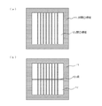
例えば、図6(a)に、長手方向に長いライン&スペースパターン(長寸法L&Sパターン)が示されている。このような長寸法L&Sパターンにおいては、マスク製造時においてパターンが図6(b)に示すようによれるという問題が生じている。また、図2(a)には、長いラインを一辺のみで支えている構造をとっている。このようなパターンでは、ラインの根元で折れ易いという問題を有している。また、図3(a)には、長いL字パターンを小さな領域で支えるという構造をとっている。これも図2の場合と同様に支点となる領域において亀裂が生じて折れやすいという問題を有している。また、図4(a)には、大面積パターンを小さな領域で支えるという構造をとっている。このようなパターンでは支点となる領域において亀裂が生じ折れやすいという問題を有している。
【0016】
また、図5(a)には、一般的にドーナツパターンと呼ばれるパターンが示されている。このような中空に浮いたパターンは、開口によってパターンを形成するステンシルマスクで加工することが不可能である。このようにステンシルマスクでは、その構造上、加工困難もしくは加工不可能なパターンが存在する。
【0017】
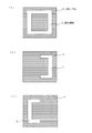
そこで、この問題を解決するために、例えば、図7(a)のようなドーナツパターンを図7(b)と図7(c)のように2枚のマスクに分割し、2回露光を組み合わせて所望のパターン(図7(a))を形成する方法がある。この方法は例えば特開平1−199384号公報に開示されている。
【0018】
この技術は、ステンシルマスクにおいて加工不可能であるパターンを形成することができるという点に関しては一応の効果を奏している。しかしながら、この技術では、複数のマスクを製作し複数回の露光を組み合わせなければならないことから、マスクを使ったスループット向上というメリットを少なからず失効させてしまう。また、マスクコストも高くなってしまう。
【0019】
また、例えば、図8(a)のようなドーナツパターンを図8(b)のように、解像限界以下の細いビーム非透過パターンでドーナツパターンを支持するようにしてアパーチャを作成するという方法がある。この方法は、例えば特開昭61−183926号公報に開示されている。
【0020】
この技術は、パターンの幅がある程度以下であればパターンが消失してしまうことにより、ステンシルマスクにおいて加工不可能であるパターンを形成することができるという点に関しては一応の効果を奏している。しかしながら、この技術では、解像限界以下の細いビーム非透過パターン83を精度よくマスク上に加工するのは困難であり、また、大面積パターンを解像限界以下の細いビーム非透過パターン83で支えるには強度不足であり、やはりマスクが破損し易いという問題がある。
【0021】
本発明は、上記問題点に鑑みてなされたものであって、その主たる目的は、長寸法L&Sパターンや大面積パターン、また、ドーナツ状のパターンを有する場合においても、これらのパターンを確実に保持することができる電子ビーム露光用マスク及び該スクを用いた露光方法を提供することにある。
【0022】
【問題を解決するための手段】
上記目的を達成するため、本発明の電子ビーム露光用マスクは、電子ビーム透過領域をドライエッチングにより開口して形成される電子ビーム露光用マスクにおいて強度が弱く破損し易いパターンに対して、該パターンの形状を維持可能な所定の強度を有する補強用の梁を設け、補強用の梁は、電子ビームによる露光によってパターンが形成される太さを有し、かつ前記電子ビーム透過領域となる開口内に設けられているものである。
【0023】
また、本発明の電子ビーム露光用マスクを用いた電子ビーム露光方法は、電子ビーム透過領域をドライエッチングにより開口して形成されるマスクを用いた電子ビーム露光方法において、強度が弱く破損し易いパターンに対して、該パターンの形状を維持可能な所定の強度を有する補強用の梁を設けたマスクを用いてパターンを転写するステップと、前記マスクを外し、前記梁の領域に対してポイント電子ビーム露光方式もしくは可変成形電子ビーム露光方式で露光するステップとを有するものである。
【0024】
本発明においては、前記パターンが、L&Sパターン、一端のみで支持されるパターン、又は、島状のパターンのいずれかを含むことが好ましい。
【0025】
このように、本発明は上記構成により、長寸法L&Sパターンや大面積パターン、また、ドーナツ状のパターンを確実に保持することができ、また、マスクを用いてパターン露光を行った後、梁の部分のみポイント電子ビーム露光方式もしくは可変成形電子ビーム露光方式で別途露光を行うため、梁の部分が残ることがなく、所望のパターンを形成することができる。
【0026】
【発明の実施の形態】
本発明に係る電子ビーム露光用マスクを用いた露光方法は、その好ましい一実施の形態において、強度が弱く破損し易いパターン(例えば、長寸法L&Sパターンや一端のみが支持される大面積パターン、また、ドーナツ状のパターン)に対して、該パターンの形状を維持可能な所定の強度を有する補強用の梁を所定の領域(たとえば、長寸法L&Sパターンに対しては、ラインの長手中央においてラインに略直交する方向、一端のみが支持される大面積パターンに対しては他端側、また、ドーナツ状のパターンに対しては周囲の数カ所)に設けたステンシルマスクを形成し、このパターン補強を施したマスクを用いてパターンを露光する第1の工程と、該マスクを外し、梁の領域に対してポイント電子ビーム露光方式もしくは可変成形電子ビーム露光方式を用いて露光する第2の工程とを組み合わせ、最終的に所望のパターンを形成するものである。
【0027】
【実施例】
上記した本発明の実施の形態についてさらに詳細に説明すべく、本発明の一実施例に係る電子ビーム露光用マスク及び該マスクを用いた露光方法について、図1乃至図5を参照して説明する。図1乃至図5は、本発明の一実施例に係る電子ビームプロジェクション露光方式(Electron Beam Projection Lithography、略してEPL)用ステンシルマスクの構造を模式的に示す平面図である。
【0028】
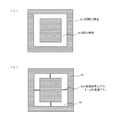
本実施例のステンシルマスクは、例えば、8インチシリコンウェハにおいて化学ガスを用いたドライエッチング手法により開口加工して形成される。ここでは、ハッチング領域が非開口領域11(シリコン)、白色領域が開口領域12(空間に何も存在しない領域)を示している。
【0029】
先ず、所望のパターンをマスク上に形成する場合に、そのパターンが図1(a)のような長寸法のライン・アンド・スペース(L&S)パターンであると、マスク製造時、及び、電子ビーム露光時における応力発生(熱ストレス、振動等)により、パターンがよれて密着してしまうという問題が生じる。従ってこのようなパターンはステンシルマスクでは形成困難または形成できたとしても破損し易い状況となる。
【0030】
そこで、図1(b)に示すように、斜線領域で示される梁13を入れて、L&Sパターンの長手方向の長さを短縮することで、マスクの破損を防ぐことができる。ここで、この梁13は、マスクの破損を十分防止できるような寸法を有することを特徴とする。
【0031】
そして、図1(b)に示すようなステンシルマスクを使って一括電子ビーム露光を行い、続いて、同一装置内において、同一の電子ビーム光源(電子銃)を使って、可変成形電子ビーム露光方式で梁13の領域を露光して、最終的に図1(a)に示す所望のパターンを形成することができる。
【0032】
また、図2(a)のような長いラインを一辺のみで支えている構造をとっているパターンでは、ラインの根元で折れ易いという問題を有している。これに対して、図2(b)のようにパターン強度を補強するように梁23を入れれば、図1の場合と同様にして所望のパターンを形成することができる。
【0033】
また、図3(a)のような長いL字パターンを小さな領域で支えるという構造をとっているパターンでは、支点となる領域において亀裂が生じて折れやすいという問題を有している。これに対して、図3(b)のようにパターン強度を補強するように梁33を入れれば図1の場合と同様にして所望のパターンを形成することができる。
【0034】
また、図4(a)のような大面積パターンを小さな領域で支えるという構造をとっているパターン、支点となる領域において亀裂が生じ折れやすいという問題を有している。これに対して、図4(b)のようにパターン強度を補強するように梁43を入れれば図1の場合と同様にして所望のパターンを形成することができる。
【0035】
また、図5(a)には、一般的にドーナツパターンと呼ばれるパターンであり、このような中空に浮いたパターンは、開口によってパターンを形成するステンシルマスクで加工することが不可能である。これに対して、図5(b)のようにパターン強度を補強するように梁53を入れれば、図1の場合と同様にして所望のパターンを形成することができる。
【0036】
なお、本実施例では、電子ビーム・プロジェクション露光方式用マスクにおいて本発明の構造を適用した例について記載したが、本発明は上記実施例に限定されるものではなく、これを部分一括電子ビーム露光用マスク、電子ビーム露光用メンブレン型マスクに対して適用しても、同様の効果が得られる。
【0037】
また、梁の領域を可変成形電子ビーム方式で露光する場合について記載したが、これをポイント電子ビーム方式で露光する場合に適用しても、同様の効果が得られる。
【0038】
また、マスクに照射する電子ビーム光源(電子銃)と、梁を露光する際に用いる可変成形電子ビーム露光の電子ビーム光源(電子銃)とを同一のものを使用する場合について説明したが、これをマスク用と可変成形用とで異なる電子ビーム光源(電子銃)を使う場合に適用しても、同様の効果が得られる。
【0039】
更に、マスクを用いた電子ビーム露光と、可変成形電子ビーム露光とを同一のチャンバー装置内で行うものとして説明したが、これを異なる装置で個別に露光する場合に適用しても、同様の効果が得られる。
【0040】
【発明の効果】
以上説明したように、本発明の電子ビーム露光用マスク及び該マスクを用いた露光方法によれば、長寸法L&Sパターンや大面積パターン、また、ドーナツ状のパターンを有するステンシルマスクにおいても、所定の強度を有する梁を設けることによってこれらのパターンを確実に保持することができ、また、上記ステンシルマスクを用いて電子ビームプロジェクション露光方式等で露光した後、梁の部分のみを可変成形電子ビーム方式又はポイント電子ビーム方式で露光することにより、所望のパターンを確実に形成することができる。
【図面の簡単な説明】
【図1】本発明の一実施例に係る電子ビームプロジェクション露光方式用ステンシルマスクの構造を模式的に示す平面図である。
【図2】本発明の一実施例に係る電子ビームプロジェクション露光方式用ステンシルマスクの構造を模式的に示す平面図である。
【図3】本発明の一実施例に係る電子ビームプロジェクション露光方式用ステンシルマスクの構造を模式的に示す平面図である。
【図4】本発明の一実施例に係る電子ビームプロジェクション露光方式用ステンシルマスクの構造を模式的に示す平面図である。
【図5】本発明の一実施例に係る電子ビームプロジェクション露光方式用ステンシルマスクの構造を模式的に示す平面図である。
【図6】従来のステンシルマスクの問題点を示す図である。
【図7】従来のドーナツパターンの形成方法を示す図である。
【図8】従来のドーナツパターンの構造を示す図である。
【符号の説明】
11、21、31、41、51、61、71、81 非開口領域
12、22、32、42、52、62、72、82 開口領域
13、23、33、43、53 梁
63 よれた領域
83 ビーム非透過パターン[0001]
BACKGROUND OF THE INVENTION
The present invention relates to an electron beam exposure mask and an exposure method using the mask, and more particularly to an electron beam exposure stencil having a pattern that is structurally easily damaged, such as a long dimension L & S pattern, a large area pattern, and a donut-shaped pattern. The present invention relates to a mask and an exposure method using the mask.
[0002]
[Prior art]
In recent years, with the increase in the density of integrated circuit devices, there has been a demand for ultra-fine processing technology for forming semiconductor elements and wirings for forming integrated circuits, and the development of techniques for realizing them has become an urgent issue. ing. For example, in order to form a fine pattern having a line width of 0.1 μm or less, there is a technique of performing fine patterning using an electron beam when exposing a resist film.
[0003]
The electron beam has an essentially high resolution because the wavelength as a material wave is very short compared to other exposure techniques and the diffraction aberration is negligibly small. However, with the conventional electron beam exposure technology (variable shaping electron beam exposure method), exposure is performed while directly painting a pattern with an electron beam shaped into a rectangle with a size of about several μm. It is a drawback. This variable shaped electron beam exposure system is described in detail in, for example, Japanese Patent Application Laid-Open No. 7-21626.
[0004]
In order to eliminate the low throughput in the variable shaped electron beam exposure method, a technique called partial batch electron beam exposure (also called cell projection exposure or block exposure) method has been put into practical use. This partial collective electron beam exposure technique is described in detail, for example, in JP-A-7-161605.
[0005]
This partial collective electron beam exposure technology is a stencil type electron beam mask (stencil mask, aperture, partial collective mask, cell projection mask, or block) in which a pattern repeatedly present in a device pattern is formed in Si having a film thickness of about 20 μm. The area pattern of several μm square is transferred at once using a mask. As a result, the number of electron beam shots is greatly reduced from the conventional variable shaped electron beam exposure method, and throughput can be improved.
[0006]
However, even with this partial batch electron beam exposure method, a non-repeatable pattern in a device pattern is drawn while directly painting the pattern with an electron beam formed into a rectangle of about several μm (variable shaped electron beam exposure). In consideration of mass production of devices, further improvement in throughput is required.
[0007]
Therefore, in recent years, as an electron beam exposure method aiming at dramatically higher throughput than the partial batch electron beam exposure method, a mask having a circuit pattern of one whole semiconductor chip is prepared, and an electron beam is applied to a certain area of the mask. There has been proposed an electron beam large area batch exposure apparatus that irradiates and reduces and transfers an image of a pattern in the irradiation range by a projection lens. This technique is generally called an electron beam projection exposure system (EPL for short).
[0008]
This EPL method is described in detail in, for example, Japanese Patent Application Laid-Open No. 2000-58446. In the variable shaped electron beam exposure method and the partial batch electron beam exposure method that have been used in the past, the area to be transferred at one time is as small as about 5 μm square, but in the above EPL technology, the batch transfer area is about 250 μm square. It is expected to greatly increase the throughput.
[0009]
As described above, the electron beam exposure technique is changing from the conventional variable shaped electron beam exposure method that does not use a mask to a partial batch electron beam exposure method that uses a mask or an EPL method in order to improve throughput.
[0010]
Here, the masks used in the electron beam exposure technique are roughly classified into two types: a membrane mask and a stencil mask. The stencil mask is described in, for example, Japanese Patent Application Laid-Open No. 5-216216. The stencil mask is a mask having an open region (no substance is present in the space), and the open region corresponds to an electron transmission region, and the non-open region corresponds to an electron scattering region. Usually, a silicon wafer is processed by opening a pattern by a dry etching method using a chemical gas.
[0011]
The greatest advantage of the stencil mask is its high contrast. Since there is no substance in the open area of the stencil mask, basically the electrons pass through without being scattered, and basically the silicon exists with a certain thickness in the open area. The electrons are scattered and not transmitted. However, the biggest disadvantage of stencil masks is that due to their structure, the pattern is formed by opening, so the mask strength, such as long dimension line and space (L & S) patterns and patterns that support large areas in small areas, etc. There will be a weak pattern. If such a weak pattern is to be processed on the mask, the mask is likely to be damaged. In addition, a generally floating pattern called a donut pattern cannot be formed with a stencil mask.
[0012]
One membrane mask is described in detail, for example, in Japanese Patent Application No. 5-62888. The membrane mask is formed by forming an electron scattering film on the electron transmission film and patterning only the electron scattering film. That is, since electrons are scattered in the region where the electron scattering film remains on the electron transmission film, the electrons are basically not transmitted. In addition, in the region where the electron scattering film does not exist on the electron permeable film (that is, the region where only the electron permeable film exists), since electrons are less likely to be scattered, the electrons are basically transmitted at a certain rate. It will be.
[0013]
However, even in an electron transmission film, electrons are scattered at a certain ratio, so that the contrast cannot be increased as much as a stencil mask that forms a pattern with an opening. However, since the electron scatterer is positioned on the electron permeable film, it is advantageous in terms of mask strength, and even a pattern that is difficult or impossible to form with a stencil mask can be formed with almost no problem.
[0014]
[Problems to be solved by the invention]
In the electron beam exposure technique, the partial batch electron beam exposure method has a track record and there is a tendency to use many stencil masks that are advantageous in terms of resolution. However, as described above, the stencil mask has a pattern that is difficult or impossible to form due to its structure.
[0015]
For example, FIG. 6A shows a long line & space pattern (long dimension L & S pattern) in the longitudinal direction. In such a long dimension L & S pattern, there is a problem that the pattern is distorted as shown in FIG. FIG. 2A shows a structure in which a long line is supported by only one side. Such a pattern has a problem of being easily broken at the base of the line. FIG. 3A shows a structure in which a long L-shaped pattern is supported by a small area. Similar to the case of FIG. 2, this also has a problem that a crack is generated in the region serving as a fulcrum and is easily broken. 4A has a structure in which a large area pattern is supported by a small region. In such a pattern, there is a problem that a crack is generated in a region serving as a fulcrum and is likely to be broken.
[0016]
FIG. 5A shows a pattern generally called a donut pattern. Such a pattern floating in the hollow cannot be processed with a stencil mask that forms a pattern by opening. Thus, in the stencil mask, there are patterns that are difficult or impossible to process due to the structure.
[0017]
In order to solve this problem, for example, a donut pattern as shown in FIG. 7A is divided into two masks as shown in FIGS. 7B and 7C, and two exposures are combined. There is a method of forming a desired pattern (FIG. 7A). This method is disclosed in, for example, JP-A-1-199384.
[0018]
This technique has a temporary effect in that a pattern that cannot be processed in a stencil mask can be formed. However, in this technique, since a plurality of masks must be manufactured and combined with a plurality of exposures, the merit of improving the throughput using the masks is lost to some extent. Also, the mask cost is increased.
[0019]
Further, for example, a method of creating an aperture by supporting a donut pattern as shown in FIG. 8A by supporting a donut pattern with a thin beam non-transmission pattern below the resolution limit as shown in FIG. 8B. is there. This method is disclosed in, for example, Japanese Patent Application Laid-Open No. 61-183926.
[0020]
This technique has a temporary effect in that a pattern that cannot be processed in a stencil mask can be formed by erasing the pattern if the pattern width is less than a certain level. However, with this technique, it is difficult to accurately process a thin beam non-transmission pattern 83 below the resolution limit on the mask, and a large area pattern is supported by the thin beam non-transmission pattern 83 below the resolution limit. Is insufficient in strength and still has a problem that the mask is easily damaged.
[0021]
The present invention has been made in view of the above-mentioned problems, and its main purpose is to reliably retain these patterns even when they have long-sized L & S patterns, large-area patterns, and donut-shaped patterns. Another object of the present invention is to provide an electron beam exposure mask and an exposure method using the mask.
[0022]
[Means for solving problems]
In order to achieve the above object, an electron beam exposure mask according to the present invention has an electron beam exposure mask formed by opening an electron beam transmission region by dry etching. a beam for reinforcement having a predetermined strength that can maintain the shape of the formed beams for reinforcement have a thickness which a pattern is formed by exposure by an electron beam, and the opening serving as the electron beam transmission region Is provided .
[0023]
The electron beam exposure method using the electron beam exposure mask of the present invention is a pattern that is weak and easily damaged in the electron beam exposure method using a mask formed by opening an electron beam transmission region by dry etching. The pattern is transferred using a mask provided with a reinforcing beam having a predetermined strength capable of maintaining the shape of the pattern, and the mask is removed, and a point electron beam is applied to the beam region. And an exposure step or a variable shaped electron beam exposure step.
[0024]
In the present invention, it is preferable that the pattern includes an L & S pattern, a pattern supported only at one end, or an island-shaped pattern.
[0025]
As described above, according to the present invention, a long-sized L & S pattern, a large area pattern, or a donut-shaped pattern can be reliably held by the above-described configuration, and after performing pattern exposure using a mask, Since only the portion is separately exposed by the point electron beam exposure method or the variable shaped electron beam exposure method, the beam portion does not remain and a desired pattern can be formed.
[0026]
DETAILED DESCRIPTION OF THE INVENTION
An exposure method using an electron beam exposure mask according to the present invention, in a preferred embodiment thereof, is a pattern that is weak and easily damaged (for example, a long dimension L & S pattern, a large area pattern in which only one end is supported, , A reinforcing beam having a predetermined strength capable of maintaining the shape of the pattern is applied to a predetermined region (for example, for a long dimension L & S pattern, a line at the longitudinal center of the line). A stencil mask provided on the other end side for a large area pattern in which only one end is supported in a substantially orthogonal direction, and several surrounding areas for a donut-like pattern) is formed, and this pattern reinforcement is applied. A first step of exposing the pattern using the mask, and removing the mask and applying a point electron beam exposure method or variable shaping electron to the beam region Combining the second step of exposing using chromatography beam exposure method, and forms a final desired pattern.
[0027]
【Example】
In order to describe the above-described embodiment of the present invention in more detail, an electron beam exposure mask and an exposure method using the mask according to an embodiment of the present invention will be described with reference to FIGS. . 1 to 5 are plan views schematically showing the structure of a stencil mask for electron beam projection lithography (abbreviated as EPL) according to an embodiment of the present invention.
[0028]
The stencil mask of this embodiment is formed, for example, by performing an opening process on a 8-inch silicon wafer by a dry etching method using a chemical gas. Here, the hatching area indicates the non-opening area 11 (silicon), and the white area indicates the opening area 12 (area where nothing exists in the space).
[0029]
First, when a desired pattern is formed on a mask, if the pattern is a long dimension line and space (L & S) pattern as shown in FIG. Due to the occurrence of stress (thermal stress, vibration, etc.) at the time, there arises a problem that the patterns come into close contact with each other. Therefore, such a pattern is difficult to form with a stencil mask, or even if it can be formed, it is likely to be damaged.
[0030]
Therefore, as shown in FIG. 1B, the mask 13 can be prevented from being damaged by inserting a beam 13 indicated by a hatched area and shortening the length in the longitudinal direction of the L & S pattern. Here, the beam 13 has a dimension that can sufficiently prevent damage to the mask.
[0031]
Then, collective electron beam exposure is performed using a stencil mask as shown in FIG. 1 (b), and then variable shaping electron beam exposure method using the same electron beam light source (electron gun) in the same apparatus. Thus, the region of the beam 13 can be exposed to form a desired pattern as shown in FIG.
[0032]
Further, the pattern having a structure in which a long line as shown in FIG. 2A is supported by only one side has a problem that it is easily broken at the root of the line. On the other hand, if the beam 23 is inserted so as to reinforce the pattern strength as shown in FIG. 2B, a desired pattern can be formed in the same manner as in FIG.
[0033]
In addition, the pattern having a structure in which a long L-shaped pattern as shown in FIG. 3A is supported in a small region has a problem that a crack is easily generated in the region serving as a fulcrum. In contrast, if a beam 33 is inserted so as to reinforce the pattern strength as shown in FIG. 3B, a desired pattern can be formed in the same manner as in FIG.
[0034]
In addition, there is a problem that a pattern having a structure in which a large area pattern as shown in FIG. 4A is supported by a small region and a crack is easily generated in a region serving as a fulcrum. In contrast, if a beam 43 is inserted so as to reinforce the pattern strength as shown in FIG. 4B, a desired pattern can be formed in the same manner as in FIG.
[0035]
FIG. 5A shows a pattern generally called a donut pattern, and such a floating pattern cannot be processed with a stencil mask that forms a pattern by an opening. On the other hand, if the
[0036]
In this embodiment, the example in which the structure of the present invention is applied to the mask for the electron beam projection exposure system is described. However, the present invention is not limited to the above embodiment, and this is applied to partial collective electron beam exposure. The same effect can be obtained even when applied to a membrane mask for electron beam and membrane type mask for electron beam exposure.
[0037]
Further, the case where the beam region is exposed by the variable shaped electron beam method has been described, but the same effect can be obtained even when the beam region is exposed by the point electron beam method.
[0038]
In addition, the case where the same electron beam light source (electron gun) for irradiating the mask and the electron beam light source (electron gun) for variable shaping electron beam exposure used for exposing the beam has been described. The same effect can be obtained by applying the electron beam light source (electron gun) for the mask and the variable shaping.
[0039]
Further, the electron beam exposure using the mask and the variable shaped electron beam exposure have been described as being performed in the same chamber apparatus, but the same effect can be obtained even when the exposure is individually performed by different apparatuses. Is obtained.
[0040]
【The invention's effect】
As described above, according to the electron beam exposure mask of the present invention and the exposure method using the mask, even in a stencil mask having a long dimension L & S pattern, a large area pattern, or a donut-shaped pattern, By providing a beam having strength, these patterns can be securely held, and after exposure by an electron beam projection exposure method or the like using the stencil mask, only the beam part is formed by a variable shaped electron beam method or By exposing by the point electron beam method, a desired pattern can be reliably formed.
[Brief description of the drawings]
FIG. 1 is a plan view schematically showing the structure of an electron beam projection exposure stencil mask according to an embodiment of the present invention.
FIG. 2 is a plan view schematically showing the structure of an electron beam projection exposure stencil mask according to an embodiment of the present invention.
FIG. 3 is a plan view schematically showing the structure of an electron beam projection exposure stencil mask according to an embodiment of the present invention.
FIG. 4 is a plan view schematically showing the structure of an electron beam projection exposure stencil mask according to an embodiment of the present invention.
FIG. 5 is a plan view schematically showing the structure of an electron beam projection exposure stencil mask according to an embodiment of the present invention.
FIG. 6 is a diagram showing a problem of a conventional stencil mask.
FIG. 7 is a diagram illustrating a conventional method for forming a donut pattern.
FIG. 8 is a diagram showing the structure of a conventional donut pattern.
[Explanation of symbols]
11, 21, 31, 41, 51, 61, 71, 81
Claims (5)
強度が弱く破損し易いパターンに対して、該パターンの形状を維持可能な所定の強度を有する補強用の梁を設け、
前記補強用の梁は、電子ビームによる露光によってパターンが形成される太さを有し、かつ前記電子ビーム透過領域となる開口内に設けられていることを特徴とする電子ビーム露光用マスク。In an electron beam exposure mask formed by opening an electron beam transmission region by dry etching,
For a pattern that is weak and easily damaged, a reinforcing beam having a predetermined strength capable of maintaining the shape of the pattern is provided,
The beam for reinforcement, the electron beam exposure mask, characterized in that provided in an opening have a thickness which a pattern is formed by exposure by an electron beam, and the said electron beam transmission region.
強度が弱く破損し易いパターンに対して、該パターンの形状を維持可能な所定の強度を有する補強用の梁を設けたマスクを用いてパターンを転写するステップと、
前記マスクを外し、前記梁の領域に対してポイント電子ビーム露光方式もしくは可変成形電子ビーム露光方式で露光するステップと、
を少なくとも有することを特徴とする電子ビーム露光方法。In an electron beam exposure method using a mask formed by opening an electron beam transmission region by dry etching,
Transferring the pattern using a mask provided with a reinforcing beam having a predetermined strength capable of maintaining the shape of the pattern for a pattern that is weak and easily damaged; and
Removing the mask and exposing the beam region by a point electron beam exposure method or a variable shaped electron beam exposure method;
An electron beam exposure method comprising:
強度が弱く破損し易いパターンに対して、該パターンの形状を維持可能な所定の強度を有する補強用の梁を設けたマスクを用いてパターンを転写するステップと、
前記マスクを外し、前記梁の領域に対してポイント電子ビーム露光方式もしくは可変成形電子ビーム露光方式で露光するステップと、
を少なくとも有することを特徴とする半導体装置の製造方法。In a manufacturing method of a semiconductor device using a mask formed by opening an electron beam transmission region by dry etching,
Transferring the pattern using a mask provided with a reinforcing beam having a predetermined strength capable of maintaining the shape of the pattern for a pattern that is weak and easily damaged; and
Removing the mask and exposing the beam region by a point electron beam exposure method or a variable shaped electron beam exposure method;
A method for manufacturing a semiconductor device, comprising:
Priority Applications (1)
| Application Number | Priority Date | Filing Date | Title |
|---|---|---|---|
| JP2001080327A JP4801268B2 (en) | 2001-03-21 | 2001-03-21 | Electron beam exposure mask, electron beam exposure method, and semiconductor device manufacturing method |
Applications Claiming Priority (1)
| Application Number | Priority Date | Filing Date | Title |
|---|---|---|---|
| JP2001080327A JP4801268B2 (en) | 2001-03-21 | 2001-03-21 | Electron beam exposure mask, electron beam exposure method, and semiconductor device manufacturing method |
Publications (2)
| Publication Number | Publication Date |
|---|---|
| JP2002280290A JP2002280290A (en) | 2002-09-27 |
| JP4801268B2 true JP4801268B2 (en) | 2011-10-26 |
Family
ID=18936626
Family Applications (1)
| Application Number | Title | Priority Date | Filing Date |
|---|---|---|---|
| JP2001080327A Expired - Fee Related JP4801268B2 (en) | 2001-03-21 | 2001-03-21 | Electron beam exposure mask, electron beam exposure method, and semiconductor device manufacturing method |
Country Status (1)
| Country | Link |
|---|---|
| JP (1) | JP4801268B2 (en) |
Families Citing this family (5)
| Publication number | Priority date | Publication date | Assignee | Title |
|---|---|---|---|---|
| JP2006260713A (en) | 2005-03-18 | 2006-09-28 | Toshiba Corp | Recording medium, recording and reproducing device, and recording and reproducing method |
| JP4542953B2 (en) | 2005-06-10 | 2010-09-15 | 株式会社東芝 | Magnetic disk medium and magnetic recording / reproducing apparatus |
| JP2007042869A (en) | 2005-08-03 | 2007-02-15 | Toyota Motor Corp | Stencil mask, its manufacturing method, its using method and method of manufacturing semiconductor device |
| JP4533854B2 (en) | 2006-03-06 | 2010-09-01 | 株式会社東芝 | Magnetic recording / reproducing apparatus, magnetic recording method, and magnetic recording / reproducing method |
| JP5256820B2 (en) * | 2008-03-31 | 2013-08-07 | 大日本印刷株式会社 | Manufacturing method of pattern forming body by vacuum ultraviolet light |
Family Cites Families (9)
| Publication number | Priority date | Publication date | Assignee | Title |
|---|---|---|---|---|
| JPS60262422A (en) * | 1984-06-11 | 1985-12-25 | Sanyo Electric Co Ltd | Mask pattern correcting method |
| JPS62262422A (en) * | 1986-05-08 | 1987-11-14 | Nec Corp | Formation of tisi2 film |
| JPH0779075B2 (en) * | 1990-02-21 | 1995-08-23 | 株式会社東芝 | Electron beam exposure system |
| JP2746098B2 (en) * | 1994-01-19 | 1998-04-28 | 日本電気株式会社 | Aperture for electron beam writing and electron beam writing method |
| JPH10189442A (en) * | 1996-11-07 | 1998-07-21 | Nikon Corp | Apparatus and method for exposure |
| JP3839962B2 (en) * | 1998-06-25 | 2006-11-01 | キヤノン株式会社 | Charged beam mask and device manufacturing method using the mask |
| JP2000260694A (en) * | 1999-03-09 | 2000-09-22 | Nikon Corp | Mask for transferring pattern and charged particle beam transfer exposure method |
| JP2001035780A (en) * | 1999-07-23 | 2001-02-09 | Nikon Corp | Mask for charged particle beam exposure and manufacture of semiconductor element |
| JPWO2002021582A1 (en) * | 2000-09-05 | 2004-01-15 | Hoya株式会社 | Transfer mask, transfer mask pattern dividing method, and transfer mask manufacturing method |
-
2001
- 2001-03-21 JP JP2001080327A patent/JP4801268B2/en not_active Expired - Fee Related
Also Published As
| Publication number | Publication date |
|---|---|
| JP2002280290A (en) | 2002-09-27 |
Similar Documents
| Publication | Publication Date | Title |
|---|---|---|
| JP2000091191A (en) | Electron beam aligning mask, method therefor, and aligning device | |
| JP2000066366A (en) | Photomask and its production | |
| US6361911B1 (en) | Using a dummy frame pattern to improve CD control of VSB E-beam exposure system and the proximity effect of laser beam exposure system and Gaussian E-beam exposure system | |
| JP4801268B2 (en) | Electron beam exposure mask, electron beam exposure method, and semiconductor device manufacturing method | |
| US6887626B2 (en) | Electron beam projection mask | |
| US6352802B1 (en) | Mask for electron beam exposure and method of manufacturing semiconductor device using the same | |
| JP2004071767A (en) | Mask, exposing method, and process for fabricating semiconductor device | |
| JP3206558B2 (en) | Aperture for electron beam writing | |
| JP2000195787A (en) | Method of forming fine pattern of semiconductor element | |
| JP2004111713A (en) | Exposure mask, exposure method, and method for manufacturing semiconductor device and the exposure mask | |
| JPH1187209A (en) | Method for projecting and exposing charged particle beam | |
| KR100548532B1 (en) | Stencil mask and method of manufacturing the same | |
| US6617084B2 (en) | Electron beam mask having dummy stripe(s) and lithographic method of manufacturing a semiconductor device using an E-beam mask having at least one defective pattern | |
| JPH11168049A (en) | Manufacture of stencil mask | |
| JP2003142439A (en) | Wafer polishing method and mask | |
| JP2005044957A (en) | System and method for electron beam exposure | |
| KR100317582B1 (en) | Photomask Manufacturing Method of Semiconductor Device | |
| JP2002343295A (en) | Electron beam exposure apparatus, reduction projection optical system and method for producing device | |
| JP2000058446A (en) | Charged particle beam transfer exposure method, reticule by use thereof, and manufacture of semiconductor device | |
| JP2004103972A (en) | Exposure mask and exposure method | |
| KR101001498B1 (en) | Vsb type mask manufacturing method with reducing beam blur effect | |
| JP2004153294A5 (en) | ||
| JP2002289508A (en) | Electron beam exposure transfer mask, its manufacturing method, electron beam exposure method and electron beam exposure system | |
| JP2004241596A (en) | Method for correcting mask pattern for exposure and method for manufacturing mask for exposure | |
| JP2001007011A (en) | Method, device, and mask for correcting proximity effect and manufacture of device |
Legal Events
| Date | Code | Title | Description |
|---|---|---|---|
| A621 | Written request for application examination |
Free format text: JAPANESE INTERMEDIATE CODE: A621 Effective date: 20080219 |
|
| RD01 | Notification of change of attorney |
Free format text: JAPANESE INTERMEDIATE CODE: A7421 Effective date: 20100426 |
|
| A977 | Report on retrieval |
Free format text: JAPANESE INTERMEDIATE CODE: A971007 Effective date: 20101012 |
|
| A131 | Notification of reasons for refusal |
Free format text: JAPANESE INTERMEDIATE CODE: A131 Effective date: 20101019 |
|
| A521 | Written amendment |
Free format text: JAPANESE INTERMEDIATE CODE: A523 Effective date: 20101215 |
|
| A131 | Notification of reasons for refusal |
Free format text: JAPANESE INTERMEDIATE CODE: A131 Effective date: 20110308 |
|
| A521 | Written amendment |
Free format text: JAPANESE INTERMEDIATE CODE: A523 Effective date: 20110421 |
|
| TRDD | Decision of grant or rejection written | ||
| A01 | Written decision to grant a patent or to grant a registration (utility model) |
Free format text: JAPANESE INTERMEDIATE CODE: A01 Effective date: 20110802 |
|
| A01 | Written decision to grant a patent or to grant a registration (utility model) |
Free format text: JAPANESE INTERMEDIATE CODE: A01 |
|
| A61 | First payment of annual fees (during grant procedure) |
Free format text: JAPANESE INTERMEDIATE CODE: A61 Effective date: 20110805 |
|
| FPAY | Renewal fee payment (prs date is renewal date of database) |
Free format text: PAYMENT UNTIL: 20140812 Year of fee payment: 3 |
|
| R150 | Certificate of patent (=grant) or registration of utility model |
Free format text: JAPANESE INTERMEDIATE CODE: R150 |
|
| LAPS | Cancellation because of no payment of annual fees |