JP4792804B2 - Power supply - Google Patents
Power supply Download PDFInfo
- Publication number
- JP4792804B2 JP4792804B2 JP2005132831A JP2005132831A JP4792804B2 JP 4792804 B2 JP4792804 B2 JP 4792804B2 JP 2005132831 A JP2005132831 A JP 2005132831A JP 2005132831 A JP2005132831 A JP 2005132831A JP 4792804 B2 JP4792804 B2 JP 4792804B2
- Authority
- JP
- Japan
- Prior art keywords
- field effect
- voltage
- output
- effect transistor
- operational amplifier
- Prior art date
- Legal status (The legal status is an assumption and is not a legal conclusion. Google has not performed a legal analysis and makes no representation as to the accuracy of the status listed.)
- Expired - Fee Related
Links
Images
Description
本発明は、例えばシステムサーバ等に使用して好適な電源装置に関する。 The present invention relates to a power supply apparatus suitable for use in, for example, a system server.
一般に、システムサーバ等に使用される電源装置は、サーバの動作の信頼性を上げるため、並列運転を行うようにした電源装置が使用されている。 Generally, a power supply device used for a system server or the like is a power supply device that performs parallel operation in order to increase the reliability of server operation.
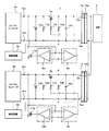
斯かる、並列運転の電源装置においては、出力電力の安定化供給が要求されている。従来、安定した出力電力を供給する並列運転の電源装置として、図3に示す如きものが提案されている。図3は、2個の同じDC−DCコンバータを使用した電源回路1及び2を並列運転するようにしたものである。
In such a parallel operation power supply apparatus, a stable supply of output power is required. Conventionally, as shown in FIG. 3, a power supply apparatus for parallel operation that supplies stable output power has been proposed. FIG. 3 shows a configuration in which
図3において、3a及び3bは夫々出力直流電圧を制御するようになされたDC−DCコンバータを示し、このDC−DCコンバータ3a及び3bの一方の出力端子4a1及び4b1を夫々逆流防止用のn形の電界効果トランジスタ5a及び5bの夫々のソースに接続し、この電界効果トランジスタの夫々のドレインを負荷6に接続する出力コネクタ7a及び7bの夫々の一方の端子7a1及び7b1に接続する。
In FIG. 3,
また、DC−DCコンバータ3a及び3bの夫々の他方の出力端子4a2及び4b2を夫々の出力コネクタ7a及び7bの夫々の他方の端子7a2及び7b2に接続する。また、電界効果トランジスタ5a及び5bのソース側即ちDC−DCコンバータ3a及び3bの夫々の一方の出力端子4a1及び4b1に得られる電圧を検出電圧として例えばパルス幅変調回路(PWM回路)等より成るDC−DCコンバータ3a及び3bの夫々の出力直流電圧を制御する制御回路8a及び8bに供給する。
Further, the other output terminals 4a2 and 4b2 of the DC-
この逆流防止用の電界効果トランジスタ5a及び5bのソース側即ちDC−DCコンバータ3a及び3bの一方の出力端子4a1及び4b1に得られる電圧を検出電圧としたのは一方の電源回路1又は2が動作中に他方の電源回路2又は1を起動することができるようにするためである。即ち、電源回路1及び2の並列運転を良好に行うことができるようにするためである。
One
また、この電界効果トランジスタ5a及び5bのソース側に得られる電圧を電界効果トランジスタ5a及び5bのオン・オフ制御増幅回路を構成する演算増幅回路9a及び9bの非反転入力端子+に供給すると共にこの電界効果トランジスタ5a及び5bの夫々のドレイン側の電圧をこの演算増幅回路9a及び9bの反転入力端子−に供給し、この演算増幅回路9a及び9bの夫々の出力端子に得られる出力信号を夫々抵抗器10a及び10bを介して電界効果トランジスタ5a及び5bの夫々のゲートに供給する。
The voltage obtained on the source side of the
この場合、電界効果トランジスタ5a及び5bのドレイン側の電圧がソース側の電圧よりも高いときは、この電界効果トランジスタ5a及び5bをオフとして、良好の電源回路1及び2の並列運転ができるようにし、この電界効果トランジスタ5a及び5bのドレイン側の電圧がソース側の電圧よりも低いときは、この電界効果トランジスタ5a及び5bをオンとし負荷6に電源を供給する。
In this case, when the voltage on the drain side of the
また、電界効果トランジスタ5a及び5bのソース側の電圧を電界効果トランジスタ5a及び5bの夫々のドレイン−ソース間の電位差を補正する電位差補正回路を構成する演算増幅回路11a及び11bの反転入力端子−に供給すると共にこの電界効果トランジスタ5a及び5bのドレイン側の電圧をこの演算増幅回路の非反転入力端子+に供給し、この演算増幅回路11a及び11bの出力側に得られる電位差補正信号を上述検出電圧と共に制御回路8a及び8bに供給する。
Further, the voltage on the source side of the
この電界効果トランジスタ5a及び5bのソース側を電解コンデンサ12a及び12bと抵抗器13a及び13bとの並列回路を介してDC−DCコンバータ3a及び3bの夫々の他方の出力端子4a2及び4b2に接続し、電界効果トランジスタ5a及び5bのドレイン側を抵抗器14a及び14bとコンデンサ15a及び15bとの並列回路を介してDC−DCコンバータ3a及び3bの夫々の他方の出力端子4a2及び4b2に接続する。
The source side of the
また、図3において、16a及び16bは夫々出力コネクタ7a及び7bに接続される並列接続された負荷6の入力コネクタである。
In FIG. 3, 16a and 16b are input connectors for the
図3の従来例においては、DC−DCコンバータ3a及び3bの夫々の出力電源ラインに逆流防止用の電界効果トランジスタ5a及び5bを設け、この電界効果トランジスタ5a及び5bのソース側の電圧を検出電圧として出力直流電圧を制御すると共にこの電界効果トランジスタ5a及び5bのドレイン−ソース間の電位差を補正する電位差補正回路を設けたので電界効果トランジスタ5a及び5bのオン抵抗、温度特性等のばらつきを吸収することができ、安定した出力電力を供給することができる。
In the conventional example of FIG. 3,
また、特許文献1には、逆流防止ダイオードを内蔵して並列運転するようにした電源装置が記載され、また特許文献2には、MOS−FETを制御手段として用いた並列運転直流電源の選択遮断回路が記載されている。
ところで、最近サーバの大容量化に伴い、電源装置に求められる出力電力も高電力になっており、負荷6に高電力の安定した出力電力を供給するという要求の中で、急激な負荷変動に対する検出電圧の応答性に対する改善が求められている。
By the way, with the recent increase in capacity of servers, the output power required for the power supply device has also become high, and in response to sudden load fluctuations in the demand for supplying stable high output power to the
然しながら、図3に示す従来の電源装置では、急激な負荷変動の検出を逆流防止用の電界効果トランジスタ5a及び5bのインピーダンスを介して行っており、この分応答性の遅れを生じると共にこの図3に示す従来の電源装置では、安定した出力電力の供給と、並列運転を弊害なく行うために、逆流防止用の電界効果トランジスタ5a及び5bの夫々のソース側の検出電圧によるDC−DCコンバータ3a及び3bの制御と、電界効果トランジスタ5a及び5bの夫々のドレイン−ソース間の電位差による電位差補正信号によるDC−DCコンバータ3a及び3bの制御との2つの電圧制御を行っているので、急激な負荷変動に対する出力直流電圧の応答性を上げるのは困難であった。
However, in the conventional power supply device shown in FIG. 3, a sudden load change is detected via the impedances of the
また、特許文献1及び2にも急激な負荷変動に対する出力直流電圧の応答性を上げるようにしたことについては何等記載されていない。
Also,
本発明は、斯かる点に鑑み、出力電力の安定供給と並列運転とを弊害なく行うと共に急激な負荷変動に対する出力直流電圧の応答性を改善することを目的とする。 SUMMARY OF THE INVENTION The present invention has been made in view of the above, and an object of the present invention is to perform stable supply of output power and parallel operation without adverse effects and to improve the response of an output DC voltage to a sudden load change.
本発明電源装置は、夫々の制御回路により出力直流電圧が制御される並列接続された複数のDC−DCコンバータの夫々の出力電源ラインに逆流防止用の第1の電界効果トランジスタが夫々接続された電源装置において、夫々の第1の電界効果トランジスタのオン・オフ制御増幅回路を構成する第1の演算増幅回路と、夫々の第1の電界効果トランジスタの負荷側となる夫々のドレイン側の電圧と夫々の第1の電界効果トランジスタの夫々のDC−DCコンバータの出力側となる夫々のソース側の電圧とを夫々比較する比較回路を構成する第2の演算増幅回路と、夫々の第2の演算増幅回路の出力端子に得られる出力信号がゲートに供給される第2の電界効果トランジスタとを有し、夫々の第1の電界効果トランジスタのソース側に得られる電圧をその第1の電界効果トランジスタのオン・オフ制御増幅回路を構成する第1の演算増幅回路の非反転入力端子の一方に供給すると共に、その第1の電界効果トランジスタのドレイン側の電圧をこの第1の演算増幅回路の反転入力端子の他方に供給し、この第1の演算増幅回路の出力端子に得られる出力信号を抵抗器を介してその第1の電界効果トランジスタのゲートに供給するようになされ、夫々のソース側の電圧が高いときには夫々の第1の電界効果トランジスタをオンとするとともに夫々のドレインの検出電圧に応じて夫々のDC−DCコンバータの夫々の出力直流電圧を制御し、夫々のドレイン側の電圧が高いときには夫々の電界効果トランジスタをオフとするとともに、夫々の比較回路を構成する第2の演算増幅回路の出力端子に得られる出力信号で、夫々のDC−DCコンバータの出力側に接続された夫々の第2の電界効果トランジスタをオンさせて、夫々の第1の電界効果トランジスタのソース側の電圧を夫々の制御回路に供給することで、夫々の制御回路で夫々のDC−DCコンバータの夫々の出力直流電圧を制御するようにしたものである。 In the power supply device of the present invention, the first field effect transistors for preventing backflow are connected to the respective output power supply lines of the plurality of DC-DC converters connected in parallel whose output DC voltage is controlled by the respective control circuits . in the power supply device, a first operational amplifier circuit constituting the on-off control amplifier circuit of the first field effect transistor of respective the voltage on the load side to become the respective drains of the first field effect transistor of the respective A second operational amplifier circuit that constitutes a comparison circuit for comparing each source side voltage on the output side of each DC-DC converter of each first field-effect transistor, and each second computation the output signal obtained at the output terminal of the amplifier circuit and a second field effect transistor being supplied to the gate, resulting in the source side of the first field effect transistor of the respective Supplies pressure to one of the non-inverting input terminal of the first operational amplifier circuits constituting the on-off control amplifier circuit of the first field effect transistor, the drain-side voltage of the first field effect transistor It was supplied to the other inverting input terminal of the first operational amplifier circuit, and supplies an output signal obtained at the output terminal of the first operational amplifier via a resistor to the gate of the first field effect transistor When each source side voltage is high, each first field effect transistor is turned on, and each output DC voltage of each DC-DC converter is controlled according to the detection voltage of each drain. , as well as turning off the field effect transistor of each when the voltage of the drain of each side is high, the output terminal of the second operational amplifier circuit constituting the comparator circuit each The second field effect transistors connected to the output side of the respective DC-DC converters are turned on by the output signals obtained in the above, and the voltages on the source side of the respective first field effect transistors are controlled. By supplying to the circuit, the respective output DC voltages of the respective DC-DC converters are controlled by the respective control circuits .
本発明によれば、逆流防止用の夫々の電界効果トランジスタの負荷側となる夫々のドレイン側の電圧と夫々の電界効果トランジスタの夫々のDC−DCコンバータの出力側となる夫々のソース側の電圧とを夫々の比較し、夫々のソース側の電圧が高いときには夫々のドレイン側の検出電圧に応じて夫々のDC−DCコンバータの夫々の出力直流電圧を制御し、夫々のドレイン側の電圧が高いときには夫々のソース側の検出電圧に応じて夫々のDC−DCコンバータの夫々の出力直流電圧を制御するようにしたので、一方の電源回路が動作中に他方の電源回路を起動することができ、並列運転を弊害なく行うことができる。 According to the present invention, the voltage on the drain side which is the load side of each field effect transistor for preventing backflow and the voltage on the source side which is the output side of each DC-DC converter of each field effect transistor. When the source side voltage is high, the output DC voltage of each DC-DC converter is controlled according to the detection voltage on the drain side, and the voltage on the drain side is high. In some cases, the output DC voltage of each DC-DC converter is controlled in accordance with the detection voltage on each source side, so that one power supply circuit can start the other power supply circuit during operation. Parallel operation can be performed without any harmful effects.
また、本発明においては、通常動作中は夫々の電界効果トランジスタの夫々のDC−DCコンバータの出力側である夫々のソース側の電圧が負荷側であるドレイン側の電圧より夫々の電界効果トランジスタのインピーダンスによる電圧降下分だけ高いので、夫々の電界効果トランジスタのドレイン側の検出電圧で夫々のDC−DCコンバータの出力直流電圧を制御し、この電界効果トランジスタのソース−ドレイン間の電位差を補正する制御を必要とすることなく出力直流電圧の安定化を図ることができると共に電圧制御系を1つとすることにより、制御系1つ分の応答性の遅れとでき、更に夫々の電界効果トランジスタのインピーダンスによる応答性の遅れが解消でき、急激な負荷変動に対する出力直流電圧の応答性が改善される。 In the present invention, during normal operation, the voltage on the source side of each DC-DC converter of each field effect transistor is higher than the voltage on the drain side on the load side. Since the voltage drop due to the impedance is high, the detection voltage on the drain side of each field effect transistor controls the output DC voltage of each DC-DC converter and corrects the potential difference between the source and drain of this field effect transistor. It is possible to stabilize the output DC voltage without the need for a single voltage control system, so that the response of one control system can be delayed, and further depending on the impedance of each field effect transistor. Response delays can be eliminated, and output DC voltage response to sudden load fluctuations is improved.
以下、図1及び図2を参照して、本発明電源装置を実施するための最良の形態の例につき説明する。図1において、図3に対応する部分には同一符号を付して示す。 Hereinafter, an example of the best mode for carrying out the power supply device of the present invention will be described with reference to FIG. 1 and FIG. In FIG. 1, parts corresponding to those in FIG.
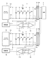
図1例2個の同じDC−DCコンバータを使用した電源回路1及び2を並列運転するようにしたものである。
図1において、3a及び3bは夫々出力直流電圧を制御するようになされたDC−DCコンバータを示し、このDC−DCコンバータ3a及び3bの一方の出力端子4a1及び4b1を夫々逆流防止用のn形の電界効果トランジスタ5a及び5bの夫々のソースに接続し、この電界効果トランジスタの夫々のドレインを負荷6に接続する出力コネクタ7a及び7bの夫々の一方の端子7a1及び7b1に接続する。
FIG. 1 shows an example in which
In FIG. 1,
また、DC−DCコンバータ3a及び3bの夫々の他方の出力端子4a2及び4b2を夫々の出力コネクタ7a及び7bの夫々の他方の端子7a2及び7b2に接続する。また、電界効果トランジスタ5a及び5bのドレイン側即ち負荷6側に得られる電圧を検出電圧として例えばパルス幅変調回路(PWM回路)等より成るDC−DCコンバータ3a及び3bの夫々の出力直流電圧を制御する制御回路8a及び8bに供給する。
Further, the other output terminals 4a2 and 4b2 of the DC-
また、この電界効果トランジスタ5a及び5bのソース側に得られる電圧を電界効果トランジスタ5a及び5bのオン・オフ制御増幅回路を構成する演算増幅回路9a及び9bの非反転入力端子+に供給すると共にこの電界効果トランジスタ5a及び5bの夫々のドレイン側の電圧をこの演算増幅回路9a及び9bの反転入力端子−に供給し、この演算増幅回路9a及び9bの夫々の出力端子に得られる出力信号を夫々抵抗器10a及び10bを介して電界効果トランジスタ5a及び5bの夫々のゲートに供給する。
The voltage obtained on the source side of the
この場合、電界効果トランジスタ5a及び5bのドレイン側の電圧がソース側の電圧よりも高いときは、この電界効果トランジスタ5a及び5bをオフとして、良好の電源回路1及び2の並列運転ができるようにし、この電界効果トランジスタ5a及び5bのドレイン側の電圧がソース側の電圧よりも低いときは、この電界効果トランジスタ5a及び5bをオンとし負荷6に電源を供給する。
In this case, when the voltage on the drain side of the
また、電界効果トランジスタ5a及び5bのソース側の電圧を接続スイッチを構成するn形電界効果トランジスタ17a及び17bの夫々のドレインに供給する。この電界効果トランジスタ17a及び17bの夫々のソースに得られる電圧を制御回路8a及び8bに夫々供給する。
The source side voltages of the
本例においては、この電界効果トランジスタ17a及び17bがオンのときは、この逆流防止用の電界効果トランジスタ5a及び5bの夫々のソース側の電圧を検出電圧として制御回路8a及び8bに供給し、この制御回路8a及び8bはこのソース側の電圧でDC−DCコンバータ3a及び3bの夫々の出力直流電圧を制御し、この電界効果トランジスタ17a及び17bがオフのときは、この制御回路8a及び8bは電界効果トランジスタ5a及び5bの夫々のドレイン側の検出電圧で、DC−DCコンバータ3a及び3bの夫々の出力直流電圧を制御するようにする。
In this example, when the
また、本例においては、電界効果トランジスタ5a及び5bのソース側の電圧を比較回路を構成する演算増幅回路18a及び18bの反転入力端子−に供給すると共にこの電界効果トランジスタ5a及び5bのドレイン側の電圧をこの演算増幅回路18a及び18bの非反転入力端子+に供給する。
In this example, the source side voltages of the
この演算増幅回路18a及び18bの出力信号を接続スイッチを構成する電界効果トランジスタ17a及び17bに供給する。従って、本例においては、電界効果トランジスタ5a及び5bの夫々のソース側の電圧がドレイン側の電圧より高いときには、電界効果トランジスタ17a及び17bはオフとなり、制御回路8a及び8bは夫々ドレイン側の検出電圧で制御される。
The output signals of the
また、本例においては、電界効果トランジスタ5a及び5bの夫々のドレイン側の電圧がソース側の電圧より高いときには、逆流防止用の電界効果トランジスタ5a及び5bは夫々オフとなると共に電界効果トランジスタ17a及び17bはオンとなり、制御回路8a及び8bは電界効果トランジスタ5a及び5bの夫々のソース側の検出電圧で制御される。
In this example, when the drain side voltages of the
この電界効果トランジスタ5a及び5bのソース側を電解コンデンサ12a及び12bと抵抗器13a及び13bとの並列回路を介してDC−DCコンバータ3a及び3bの夫々の他方の出力端子4a2及び4b2に接続し、電界効果トランジスタ5a及び5bのドレイン側を抵抗器14a及び14bとコンデンサ15a及び15bとの並列回路を介してDC−DCコンバータ3a及び3bの夫々の他方の出力端子4a2及び4b2に接続する。
The source side of the
また、図1において、16a及び16bは夫々出力コネクタ7a及び7bに接続される並列接続された負荷6の入力コネクタである。
In FIG. 1, 16a and 16b are input connectors for the
本例によれば、逆流防止用の夫々の電界効果トランジスタ5a及び5bの負荷側となる夫々のドレイン側の電圧と夫々の電界効果トランジスタ5a及び5bの夫々のDC−DCコンバータ3a及び3bの出力側となる夫々のソース側の電圧とを夫々の比較し、夫々のソース側の電圧が高いときには夫々のドレイン側の検出電圧に応じて夫々のDC−DCコンバータ3a及び3bの夫々の出力直流電圧を制御し、夫々のドレイン側の電圧が高いときには夫々のソース側の検出電圧に応じて夫々のDC−DCコンバータ3a及び3bの夫々の出力直流電圧を制御するようにしたので、一方の電源回路が動作中に他方の電源回路を起動することができ、並列運転を弊害なく行うことができる。
According to this example, the voltage on the drain side which is the load side of each
即ち、本例によれば、起動時は逆流防止用の電界効果トランジスタ5a又は5bのソース側の電圧がドレイン側の電圧より低いにで、接続スイッチを構成する電界効果トランジスタ17a又は17bがオンとなり、電界効果トランジスタ5a又は5bのソース側の電圧を検出電圧としてDC−DCコンバータ3a又は3bの出力直流電圧を制御する。
In other words, according to this example, the
このときは、電界効果トランジスタ5a又は5bのソース側の電圧がドレイン側の電圧より低いので、この電界効果トランジスタ5a又は5bはオフであり、動作中の電源回路1又は2の影響を受けずに並列運転の起動を行うことができる。
At this time, since the voltage on the source side of the
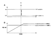
このDC−DCコンバータ3a又は3bの出力直流電圧が立ち上がる途中で、図2Bに示す如く、この電界効果トランジスタ5a又は5bのソース側電圧V1がドレイン側電圧V2と比較して同電位以上になると、図2AのE点に示す如く、電界効果トランジスタ17a又は17bをオフさせ電界効果トランジスタ5a又は5bのドレイン側の電圧V2を検出電圧として、DC−DCコンバータ3a又は3bの出力直流電圧を制御するようにすると同時に電界効果トランジスタ5a又は5bをオンとし、DC−DCコンバータ3a又は3bの出力直流電圧を負荷6に供給する如くする。
When the output DC voltage of the DC-
また、本例においては、通常動作中は夫々の電界効果トランジスタ5a及び5bの夫々のDC−DCコンバータ3a及び3bの出力側である夫々のソース側の電圧が負荷6側であるドレイン側の電圧より夫々の電界効果トランジスタ5a及び5bのインピーダンスによる電圧降下分だけ高いので、夫々の電界効果トランジスタ5a及び5bのドレイン側の検出電圧で夫々のDC−DCコンバータ3a及び3bの出力直流電圧を制御し、この電界効果トランジスタ5a及び5bのソース−ドレイン間の電位差を補正する制御を必要とすることなく出力直流電圧の安定化を図ることができると共に電圧制御系を1つとすることにより、制御系1つ分の応答性の遅れとでき、更に夫々の電界効果トランジスタ5a及び5bのインピーダンスによる応答性の遅れが解消でき、急激な負荷変動に対する出力直流電圧の応答性が改善される。
In this example, during normal operation, the voltage on the source side which is the output side of each DC-
尚、上述例は、2つの電源回路1及び2を並列運転する例につき述べたが、本発明を3つ以上の電源回路を並列運転する場合にも適用できることは勿論である。
Although the above example has been described with respect to an example in which two
また、本発明は上述例に限ることなく、本発明の要旨を逸脱することなく、その他種々の構成が採り得ることは勿論である。 Further, the present invention is not limited to the above-described example, and various other configurations can be adopted without departing from the gist of the present invention.
1、2…電源回路、3a、3b…DC−DCコンバータ、5a、5b、17a、17b…電界効果トランジスタ、6…負荷、7a、7b…出力コネクタ、8a、8b…制御回路、9a、9b、18a、18b…演算増幅回路、16a、16b…入力コネクタ
DESCRIPTION OF
Claims (2)
前記第1の電界効果トランジスタのオン・オフ制御増幅回路を構成する第1の演算増幅回路と、
前記第1の電界効果トランジスタの負荷側となるドレイン側の電圧と前記第1の電界効果トランジスタの前記DC−DCコンバータの出力側となるソース側の電圧とを比較する比較回路を構成する第2の演算増幅回路と、該第2の演算増幅回路の出力端子に得られる出力信号がゲートに供給される第2の電界効果トランジスタとを有し、
前記第1の電界効果トランジスタのソース側に得られる電圧を該第1の電界効果トランジスタのオン・オフ制御増幅回路を構成する前記第1の演算増幅回路の非反転入力端子の一方に供給すると共に、該第1の電界効果トランジスタのドレイン側の電圧を前記第1の演算増幅回路の反転入力端子の他方に供給し、該第1の演算増幅回路の出力端子に得られる出力信号を抵抗器を介して該第1の電界効果トランジスタのゲートに供給するようになされ、
前記ソース側の電圧が高いときには前記第1の電界効果トランジスタをオンとするとともに前記ドレインの検出電圧に応じて前記制御回路が前記DC−DCコンバータの出力直流電圧を制御し、前記ドレイン側の電圧が高いときには前記第1の電界効果トランジスタをオフとするとともに、前記比較回路を構成する第2の演算増幅回路の出力端子に得られる出力信号で、前記DC−DCコンバータの出力側に接続された第2の電界効果トランジスタをオンさせて、前記第1の電界効果トランジスタのソース側の電圧を前記制御回路に供給することで、前記制御回路で前記DC−DCコンバータの出力直流電圧を制御する
電源装置。 In a power supply apparatus in which a first field effect transistor for preventing backflow is connected to an output power supply line of a DC-DC converter in which an output DC voltage is controlled by a control circuit ,
A first operational amplifier circuit constituting an on / off control amplifier circuit of the first field effect transistor;
Second composing a comparator circuit for comparing the first said source of voltage as a DC-DC converter on the output side of the voltage between said first field effect transistor on the load side to become the drain side of the FET transistor And a second field effect transistor to which an output signal obtained at the output terminal of the second operational amplifier circuit is supplied to the gate ,
It supplies a voltage obtained at the source side of the first field effect transistor to one of the non-inverting input terminal of said first operational amplifier circuit constituting the on-off control amplifier circuit of the first field effect transistor , wherein the first drain side of the voltage of the field effect transistor is supplied to the other inverting input terminal of said first operational amplifier, a resistor the output signal obtained at the output terminal of said first operational amplifier circuit It supplies it to the gate of said first field effect transistor via,
When the source side voltage is high, the first field effect transistor is turned on, and the control circuit controls the output DC voltage of the DC-DC converter according to the detected voltage of the drain, and the drain side voltage Is high, the first field effect transistor is turned off, and the output signal obtained at the output terminal of the second operational amplifier circuit constituting the comparison circuit is connected to the output side of the DC-DC converter. By turning on the second field effect transistor and supplying the voltage on the source side of the first field effect transistor to the control circuit, the control circuit controls the output DC voltage of the DC-DC converter. apparatus.
前記夫々の第1の電界効果トランジスタのオン・オフ制御増幅回路を構成する第1の演算増幅回路と、
前記夫々の第1の電界効果トランジスタの負荷側となる夫々のドレイン側の電圧と前記夫々の第1の電界効果トランジスタの前記夫々のDC−DCコンバータの出力側となる夫々のソース側の電圧とを夫々比較する比較回路を構成する第2の演算増幅回路と、該夫々の第2の演算増幅回路の出力端子に得られる出力信号がゲートに供給される第2の電界効果トランジスタとを有し、
前記夫々の第1の電界効果トランジスタのソース側に得られる電圧を該第1の電界効果トランジスタのオン・オフ制御増幅回路を構成する前記第1の演算増幅回路の非反転入力端子の一方に供給すると共に、該第1の電界効果トランジスタのドレイン側の電圧を前記第1の演算増幅回路の反転入力端子の他方に供給し、該第1の演算増幅回路の出力端子に得られる出力信号を抵抗器を介して該第1の電界効果トランジスタのゲートに供給するようになされ、
前記夫々のソース側の電圧が高いときには前記夫々の第1の電界効果トランジスタをオンとするとともに前記夫々のドレインの検出電圧に応じて前記制御回路が前記夫々のDC−DCコンバータの夫々の出力直流電圧を制御し、
前記夫々のドレイン側の電圧が高いときには前記夫々の第1の電界効果トランジスタをオフとするとともに、前記夫々の比較回路を構成する第2の演算増幅回路の出力端子に得られる出力信号で、前記夫々のDC−DCコンバータの出力側に接続された前記夫々の第2の電界効果トランジスタをオンさせて、前記夫々の第1の電界効果トランジスタのソース側の電圧を前記夫々の制御回路に供給することで、前記夫々の制御回路で前記夫々のDC−DCコンバータの出力直流電圧を制御する
電源装置。 In the power supply apparatus in which the first field effect transistors for preventing the backflow are connected to the respective output power supply lines of the plurality of DC-DC converters connected in parallel whose output DC voltage is controlled by the respective control circuits .
A first operational amplifier circuit constituting an on / off control amplifier circuit for each of the first field effect transistors;
Said respective DC-DC converter of the voltage on the output side to become respectively the source of voltage and the respective first field effect transistor of the load side to become the respective drain of the respective first field effect transistor A second operational amplifier circuit that constitutes a comparison circuit that compares each of the second operational amplifier circuits, and a second field effect transistor that supplies an output signal obtained at the output terminal of each of the second operational amplifier circuits to the gate. ,
Supplying a voltage obtained at the source side of the first field effect transistor of the respective one of the non-inverting input terminal of said first operational amplifier circuit constituting the on-off control amplifier circuit of the first field effect transistor while the drain side of the voltage of the first field effect transistor is supplied to the other inverting input terminal of said first operational amplifier circuit, an output signal obtained at the output terminal of said first operational amplifier circuit resistance through the vessel supplies it to the gate of said first field effect transistor,
When the respective source-side voltages are high, the respective first field-effect transistors are turned on, and the control circuit controls the respective output DC of the respective DC-DC converters in accordance with the detected voltage of the respective drains. Control the voltage,
When the respective drain-side voltages are high, the respective first field effect transistors are turned off, and the output signal obtained at the output terminal of the second operational amplifier circuit constituting each of the comparison circuits, Each of the second field effect transistors connected to the output side of each DC-DC converter is turned on, and the voltage on the source side of each of the first field effect transistors is supplied to each of the control circuits. Thus, the power supply apparatus that controls the output DC voltage of each of the DC-DC converters by the respective control circuit .
Priority Applications (1)
| Application Number | Priority Date | Filing Date | Title |
|---|---|---|---|
| JP2005132831A JP4792804B2 (en) | 2005-04-28 | 2005-04-28 | Power supply |
Applications Claiming Priority (1)
| Application Number | Priority Date | Filing Date | Title |
|---|---|---|---|
| JP2005132831A JP4792804B2 (en) | 2005-04-28 | 2005-04-28 | Power supply |
Publications (2)
| Publication Number | Publication Date |
|---|---|
| JP2006311739A JP2006311739A (en) | 2006-11-09 |
| JP4792804B2 true JP4792804B2 (en) | 2011-10-12 |
Family
ID=37477919
Family Applications (1)
| Application Number | Title | Priority Date | Filing Date |
|---|---|---|---|
| JP2005132831A Expired - Fee Related JP4792804B2 (en) | 2005-04-28 | 2005-04-28 | Power supply |
Country Status (1)
| Country | Link |
|---|---|
| JP (1) | JP4792804B2 (en) |
Families Citing this family (1)
| Publication number | Priority date | Publication date | Assignee | Title |
|---|---|---|---|---|
| JP5088530B2 (en) | 2006-11-17 | 2012-12-05 | 株式会社ジェイテクト | Vehicle steering system |
Family Cites Families (2)
| Publication number | Priority date | Publication date | Assignee | Title |
|---|---|---|---|---|
| JPH0670544A (en) * | 1992-08-11 | 1994-03-11 | Fujitsu Ltd | Reverse current preventive circuit for parallel power source |
| JP2000350447A (en) * | 1999-06-01 | 2000-12-15 | Sony Corp | Unit and system for power source |
-
2005
- 2005-04-28 JP JP2005132831A patent/JP4792804B2/en not_active Expired - Fee Related
Also Published As
| Publication number | Publication date |
|---|---|
| JP2006311739A (en) | 2006-11-09 |
Similar Documents
| Publication | Publication Date | Title |
|---|---|---|
| US20110227640A1 (en) | Power supply device | |
| KR102575945B1 (en) | Switching regulator | |
| US20120056655A1 (en) | Method and system for controlling HS-NMOS power switches with slew-rate limitation | |
| CN205092772U (en) | Linear regulator control circuit | |
| JP2014086073A (en) | Low drop-out regulator | |
| JP2005327164A (en) | Voltage regulator | |
| CN108432112B (en) | DC-DC converter and semiconductor integrated circuit for driving load | |
| US7683693B2 (en) | Hot swap controller with zero loaded charge pump | |
| US9397569B2 (en) | Current control circuit with in parallel transistor modules | |
| US9748842B1 (en) | Sense circuit for voltage converter | |
| KR20160075329A (en) | Voltage regulator | |
| US9160230B2 (en) | DC/DC converter and electronic apparatus | |
| US9417645B2 (en) | Voltage regulator | |
| JP4792804B2 (en) | Power supply | |
| US20160187900A1 (en) | Voltage regulator circuit and method for limiting inrush current | |
| US20170025951A1 (en) | Combined High Side and Low Side Current Sensing | |
| US9800149B2 (en) | Switching regulator | |
| EP4254796A3 (en) | Switching circuit | |
| JP2005251130A (en) | Voltage regulator circuit with short circuit protection circuit | |
| JP2007006670A (en) | Inrush current preventing circuit | |
| JP6090846B2 (en) | Power supply device, power supply control method, and electronic device | |
| JP6549008B2 (en) | Voltage regulator | |
| JP4150009B2 (en) | Standby voltage setting circuit, standby voltage setting method, power supply apparatus, power supply control method, and power supply system | |
| JP2002010627A (en) | Dc-dc converter | |
| JP2007209121A (en) | Power system |
Legal Events
| Date | Code | Title | Description |
|---|---|---|---|
| A621 | Written request for application examination |
Free format text: JAPANESE INTERMEDIATE CODE: A621 Effective date: 20080311 |
|
| A977 | Report on retrieval |
Free format text: JAPANESE INTERMEDIATE CODE: A971007 Effective date: 20101022 |
|
| A131 | Notification of reasons for refusal |
Free format text: JAPANESE INTERMEDIATE CODE: A131 Effective date: 20101026 |
|
| A521 | Written amendment |
Free format text: JAPANESE INTERMEDIATE CODE: A523 Effective date: 20101216 |
|
| A131 | Notification of reasons for refusal |
Free format text: JAPANESE INTERMEDIATE CODE: A131 Effective date: 20110308 |
|
| A521 | Written amendment |
Free format text: JAPANESE INTERMEDIATE CODE: A523 Effective date: 20110426 |
|
| TRDD | Decision of grant or rejection written | ||
| A01 | Written decision to grant a patent or to grant a registration (utility model) |
Free format text: JAPANESE INTERMEDIATE CODE: A01 Effective date: 20110628 |
|
| A01 | Written decision to grant a patent or to grant a registration (utility model) |
Free format text: JAPANESE INTERMEDIATE CODE: A01 |
|
| A61 | First payment of annual fees (during grant procedure) |
Free format text: JAPANESE INTERMEDIATE CODE: A61 Effective date: 20110711 |
|
| FPAY | Renewal fee payment (event date is renewal date of database) |
Free format text: PAYMENT UNTIL: 20140805 Year of fee payment: 3 |
|
| LAPS | Cancellation because of no payment of annual fees |