JP4792309B2 - Electro-optic element - Google Patents
Electro-optic element Download PDFInfo
- Publication number
- JP4792309B2 JP4792309B2 JP2006081595A JP2006081595A JP4792309B2 JP 4792309 B2 JP4792309 B2 JP 4792309B2 JP 2006081595 A JP2006081595 A JP 2006081595A JP 2006081595 A JP2006081595 A JP 2006081595A JP 4792309 B2 JP4792309 B2 JP 4792309B2
- Authority
- JP
- Japan
- Prior art keywords
- electro
- cathode
- crystal
- anode
- optic
- Prior art date
- Legal status (The legal status is an assumption and is not a legal conclusion. Google has not performed a legal analysis and makes no representation as to the accuracy of the status listed.)
- Expired - Fee Related
Links
Images


Landscapes
- Optical Modulation, Optical Deflection, Nonlinear Optics, Optical Demodulation, Optical Logic Elements (AREA)
Description
本発明は、電気光学素子に関し、より詳細には、電気光学結晶を用いて電気信号により光の位相を変える電気光学素子に関する。 The present invention relates to an electro-optical element, and more particularly to an electro-optical element that changes the phase of light by an electric signal using an electro-optical crystal.
従来、電気光学結晶を用いた様々な光機能部品が実用化されている。これら光機能部品は、電気光学結晶に電圧を印加すると、電気光学効果により結晶の屈折率が変化することを利用している。例えば、電気光学結晶を用いた光位相変調器は、結晶の屈折率の変化により、結晶を通過する光の速度を変化させて、光の位相を変化させる。また、この光位相変調器を利用して、光スイッチ、光強度変調器を構成することもできる。 Conventionally, various optical functional parts using electro-optic crystals have been put into practical use. These optical functional parts utilize the fact that when a voltage is applied to the electro-optic crystal, the refractive index of the crystal changes due to the electro-optic effect. For example, an optical phase modulator using an electro-optic crystal changes the phase of light by changing the speed of light passing through the crystal by changing the refractive index of the crystal. In addition, an optical switch and an optical intensity modulator can be configured using this optical phase modulator.
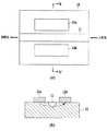
図1に、従来の光位相変調器の構成を示す(例えば、特許文献1)。LiNbO3基板10に形成された導波路11の両側に、2つの電極、陽極12aおよび陰極12bが形成されている(図1(a))。陽極12aおよび陰極12b間に、電圧を印加し、導波路11にかかる電界を変化させる(図1(b))。これにより、電気光学材料の屈折率を変化させて、導波路11を通過する光信号の位相を変調する。
FIG. 1 shows a configuration of a conventional optical phase modulator (for example, Patent Document 1). Two electrodes, an
図1に示した光位相変調器において、変調される光の位相ΔΦは、光の伝搬方向において電界の印加される部分の長さをLとし、光の波長をλとし、変化する屈折率をΔnとすると、
ΔΦ=2π×Δn×L/λ
と表される。さらに、Δnは、
Δn=−0.5n3rE
と表される。ここで、Eは導波路に印加された電界、rは一次の電気光学係数、nは屈折率である。
In the optical phase modulator shown in FIG. 1, the phase ΔΦ of light to be modulated is defined by the length of the portion to which the electric field is applied in the light propagation direction as L, the wavelength of the light as λ, and the changing refractive index. If Δn,
ΔΦ = 2π × Δn × L / λ
It is expressed. Furthermore, Δn is
Δn = −0.5n 3 rE
It is expressed. Here, E is the electric field applied to the waveguide, r is the primary electro-optic coefficient, and n is the refractive index.
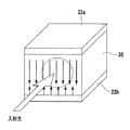
近年、電気光学係数の大きなKTa1−xNbxO3(KTN)結晶が着目されている。KTN結晶は、電気光学係数が大きいために、小さなサイズ、小さな駆動電圧で光スイッチを構成することができる。図2に、従来のKTN結晶を用いた光位相変調器の構成を示す。光位相変調器は、方形のKTN結晶20の対向する面に、陽極22aおよび陰極22bが形成されている。陽極22aおよび陰極22b間に、バイアス電界を印加し、さらにそのバイアス電界の下で、2つの電極間に信号電界を重畳する。これにより、KTN結晶20の電界が信号によって変化し、2つの電極間の屈折率が変化するので、KTN結晶20を通過する入射光の位相を信号に応じて変化させることができる。この光位相変調器を利用して、光強度変調器、光スイッチ、Qスイッチなどの光機能素子を構成することができる。
In recent years, KTa 1-x Nb x O 3 (KTN) crystals having a large electro-optic coefficient have attracted attention. Since the KTN crystal has a large electro-optic coefficient, an optical switch can be configured with a small size and a small driving voltage. FIG. 2 shows a configuration of an optical phase modulator using a conventional KTN crystal. In the optical phase modulator, an
バイアス電界は、初期位相を適切な位相に保持するために使用される。加えて、常誘電相のKTN結晶など、主に2次の電気光学効果を有する材料の場合は、バイアス電界が強いほど電気光学効果が大きくなるという特徴がある。図3に、2次の電気光学効果を有する材料における印加電圧と屈折率の関係を示す。バイアス電圧Vbiasが大きいほど、信号電圧Vsによって変調される屈折率の変化Δnは大きくなる。 The bias field is used to keep the initial phase in the proper phase. In addition, a material having a secondary electro-optic effect such as a paraelectric KTN crystal has a feature that the stronger the bias electric field, the greater the electro-optic effect. FIG. 3 shows the relationship between applied voltage and refractive index in a material having a secondary electro-optic effect. The larger the bias voltage V bias , the larger the refractive index change Δn modulated by the signal voltage V s .
しかしながら、KTN結晶は、電界を印加するとバルク結晶内の電気光学特性が一様でなくなり、偏向などの現象が起こるという問題があった。これは、図2に実線の矢印で示した電界の向きと逆方向に、陰極22bから電荷(図2に破線の矢印で示す)が結晶内部に入り込むためである。電界分布が一様でなくなると、入射光の一部が偏向し、光位相変調器として一様な変調特性が得られない。偏向の影響を抑えるために、印加するバイアス電圧を低く設定すると、良好な電気光学特性が得られないという問題があった。 However, the KTN crystal has a problem that when an electric field is applied, the electro-optical characteristics in the bulk crystal are not uniform, and a phenomenon such as deflection occurs. This is because electric charges (indicated by broken line arrows in FIG. 2) enter the inside of the crystal in the direction opposite to the direction of the electric field indicated by solid line arrows in FIG. If the electric field distribution is not uniform, a part of incident light is deflected, and uniform modulation characteristics cannot be obtained as an optical phase modulator. If the bias voltage to be applied is set low in order to suppress the influence of deflection, there is a problem that good electro-optical characteristics cannot be obtained.
本発明は、このような問題に鑑みてなされたもので、その目的とするところは、結晶内部の電界分布が一様となるようにして、良好な電気光学特性が得られる電気光学素子を提供することにある。 The present invention has been made in view of such problems, and an object of the present invention is to provide an electro-optic element capable of obtaining good electro-optic characteristics by making the electric field distribution inside the crystal uniform. There is to do.
本発明は、このような目的を達成するために、請求項1に記載の発明は、電気光学結晶を用いた電気光学素子において、前記電気光学結晶に電界を印加するための陽極および陰極を備え、前記陽極の前記電気光学結晶との接触面積は、前記陰極の前記電気光学結晶との接触面積より狭く、前記電気光学結晶はKTa 1−x Nb x O 3 (0<x<1)またはK 1−y Li y Ta 1−x Nb x O 3 (0<x<1,0<y<0.1)のいずれかであり、該電気光学結晶を常誘電相で用いることを特徴とする。 In order to achieve the above object, the present invention provides an electro-optic element using an electro-optic crystal, comprising an anode and a cathode for applying an electric field to the electro-optic crystal. , the contact area between the electro-optic crystal of the anode, the rather narrow than the contact area between the electro-optic crystal of the cathode, the electro-optical crystal KTa 1-x Nb x O 3 (0 <x <1) or Any of K 1-y Li y Ta 1-x Nb x O 3 (0 <x <1, 0 <y <0.1), wherein the electro-optic crystal is used in a paraelectric phase .
請求項2に記載の発明は、請求項1に記載の電気光学素子において、前記陽極の、前記電気光学結晶を通過する光の進行方向に垂直な方向の幅は、前記陰極の幅より狭いことを特徴とする。 According to a second aspect of the present invention, in the electro-optic element according to the first aspect, a width of the anode in a direction perpendicular to a traveling direction of light passing through the electro-optic crystal is narrower than a width of the cathode. It is characterized by.
請求項3に記載の発明は、請求項2に記載の電気光学素子において、前記陽極の幅は、前記陽極および陰極間の間隔より狭く、前記陰極の幅は、前記陽極および陰極間の間隔より広いことを特徴とする。 According to a third aspect of the present invention, in the electro-optical element according to the second aspect, the width of the anode is narrower than the distance between the anode and the cathode, and the width of the cathode is smaller than the distance between the anode and the cathode. It is wide.
請求項1、2または3に記載の前記陽極を、光の進行方向に平行に、複数に分割することができる。また、前記陰極を、光の進行方向に平行に、複数に分割することもできる。 The anode according to claim 1, 2, or 3 can be divided into a plurality of pieces in parallel with the traveling direction of light. Further, the cathode can be divided into a plurality of pieces in parallel with the light traveling direction.
以上説明したように、本発明によれば、一方の電極の電気光学結晶との接触面積と、他方の電極の電気光学結晶との接触面積とに差があるので、結晶内部の電界分布が一様となり、良好な電気光学特性を得ることが可能となる。 As described above, according to the present invention, since there is a difference between the contact area of one electrode with the electro-optic crystal and the contact area of the other electrode with the electro-optic crystal, the electric field distribution inside the crystal is uniform. Thus, good electro-optical characteristics can be obtained.
以下、図面を参照しながら本発明の実施形態について詳細に説明する。本実施形態においては、陽極と陰極のサイズを変えることにより、バルク結晶内に生ずる電界の大きさを制御する。2つの電極のうち、面積の小さい陽極に近接した部分の電界は上がり、面積の大きい陰極に近接した部分の電界は下がる。これにより、陰極から結晶内部に入り込む電荷の影響が緩和され、結晶内部の電界分布を一様にすることができる。 Hereinafter, embodiments of the present invention will be described in detail with reference to the drawings. In this embodiment, the magnitude of the electric field generated in the bulk crystal is controlled by changing the sizes of the anode and the cathode. Of the two electrodes, the electric field in the portion close to the anode with a small area increases, and the electric field in the portion close to the cathode with a large area decreases. Thereby, the influence of the electric charge entering the inside of the crystal from the cathode can be relaxed, and the electric field distribution inside the crystal can be made uniform.
図4に、本発明の実施例1にかかる電気光学素子の構成を示す。電気光学素子は、方形のKTN結晶40の対向する面に、陽極42aおよび陰極42bが形成されている。KTN結晶40の結晶軸x,y,zを図4に示したように規定する。KTN結晶40は、光の進行方向の長さ(z軸方向)5mm、幅(x軸方向)1.5mmであり、2つの電極間の厚さ(y軸方向)1.0mmの結晶である。陰極42bは、KTN結晶40の下面、全面に蒸着されている。従って、幅(x軸方向)1.5mmであり、2つの電極間の間隔1.0mmよりも広くなっている。一方、陽極42aは、幅(x軸方向)0.5mmであり、2つの電極間の間隔1.0mmよりも狭くなっている(電極セットAという)。KTN結晶40の相転移温度は0度であり、20度で動作するように温度保持されている。
FIG. 4 shows the configuration of the electro-optic element according to Example 1 of the invention. In the electro-optic element, an
一方、比較のために、陽極42aおよび陰極42bともに幅(x軸方向)1.0mmであり、2つの電極を間隔1.0mmで対向させた電気光学素子を用意しておく(電極セットBという)。
On the other hand, for comparison, an electro-optic element in which both the
電極セットAは、陰極の面積が、陽極よりも3倍大きくなっている。また、電極セットBと比較すると、陽極の面積はより小さく、陰極の面積はより大きくなっている。陽極42aおよび陰極42b間に、100Vのバイアス電圧を印加すると、電極セットAは、電極セットBよりも陰極に発生する電界が緩和されている。従って、入射光が通過する部分の電界分布が一様となり、より一様な電気光学特性を得ることができる。
In the electrode set A, the area of the cathode is three times larger than that of the anode. Moreover, compared with the electrode set B, the area of the anode is smaller and the area of the cathode is larger. When a bias voltage of 100 V is applied between the
また、陰極42bと比較して電気光学結晶との接触面積が狭い陽極42aの幅が、陽極42aおよび陰極42b間の間隔よりも狭い場合に、陰極に発生する電界の緩和は、特に有効に働く。
Further, when the width of the
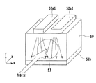
図5に、本発明の実施例2にかかる電気光学素子の構成を示す。電気光学素子は、方形のKTN結晶50の対向する面に、陽極52a1,52a2および陰極52bが形成されている。KTN結晶50は、光の進行方向の長さ(z軸方向)5mm、幅(x軸方向)1.5mmであり、2つの電極間の厚さ(y軸方向)1.0mmの結晶である。陰極52bは、KTN結晶50の下面、全面に蒸着されている。従って、幅(x軸方向)1.5mmであり、2つの電極間の間隔1.0mmよりも広くなっている。一方、陽極は2つに分割されている。陽極52a1,52a2は、それぞれ幅(x軸方向)0.2mmであり、間隔0.2mmをおいて形成されている。
FIG. 5 shows the configuration of an electro-optic element according to Example 2 of the present invention. In the electro-optic element, anodes 52a1 and 52a2 and a
陽極を2つに分割することにより、入射光が通過する部分の電界分布が、実施例1と比較してより一様となる。図4を参照すると、入射光が通過する部分43の中心、すなわち光軸を、陽極42aのz軸方向に延びる中心線と一致させると、入射光が通過する部分43の中心に電界が集中する。従って、陰極43に発生する電界の影響も大きい。そこで、図5に示したように、陽極52a1,52a2を分割することにより、入射光が通過する部分53の中心の電界を緩和し、この中心付近に集中していた陰極に発生する電界も緩和する。
By dividing the anode into two, the electric field distribution in the portion through which the incident light passes becomes more uniform as compared with the first embodiment. Referring to FIG. 4, when the center of the
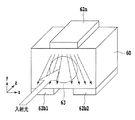
図6に、本発明の実施例3にかかる電気光学素子の構成を示す。電気光学素子は、方形のKTN結晶60の対向する面に、陽極62aおよび陰極62b1,62b2が形成されている。KTN結晶60は、光の進行方向の長さ(z軸方向)5mm、幅(x軸方向)1.5mmであり、2つの電極間の厚さ(y軸方向)1.0mmの結晶である。陽極62aは、幅(x軸方向)0.5mmであり、2つの電極間の間隔1mmよりも狭くなっている。一方、陰極は2つに分割されている。陰極62b1,62b2は、それぞれ幅(x軸方向)0.5mmであり、間隔0.5mmをおいて形成されている。
FIG. 6 shows a configuration of an electro-optic element according to Example 3 of the present invention. In the electro-optic element, an
陰極62b1,62b2と2つに分割することにより、実施例2と同様に、入射光が通過する部分63の中心の電界を緩和し、この中心付近に集中していた陰極に発生する電界も緩和する。
By dividing the cathodes 62b1 and 62b2 into two, the electric field at the center of the
図7に、本発明の実施例4にかかる電気光学素子の構成を示す。電気光学素子は、方形のKTN結晶70の上面に、陽極72aおよび陰極72bが、間隔をおいて対向して形成されている。KTN結晶70は、光の進行方向の長さ(z軸方向)5mm、幅(x軸方向)10.0mmである。2つの電極間の間隔(x軸方向)1.0mmであり、陽極72aは、幅(x軸方向)0.5mmであり、2つの電極間の間隔1.0mmよりも狭くなっている。陰極72bは、幅(x軸方向)1.5mmであり、2つの電極間の間隔1.0mmよりも広くなっている。
FIG. 7 shows a configuration of an electro-optic element according to Example 4 of the present invention. In the electro-optic element, an
実施例1〜3と同様に、面積の小さい陽極に近接した部分の電界は上がり、面積の大きい陰極に近接した部分の電界は下がる。これにより、陰極から結晶内部に入り込む電荷の影響が緩和され、結晶内部の電界分布を一様にすることができる。 As in Examples 1 to 3, the electric field in the portion close to the anode having a small area increases, and the electric field in the portion close to the cathode having a large area decreases. Thereby, the influence of the electric charge entering the inside of the crystal from the cathode can be relaxed, and the electric field distribution inside the crystal can be made uniform.
また、電気光学結晶は、KTN結晶に限らず、K1−yLiyTa1−xNbxO3(0<x<1,0<y<0.1)結晶とすることができ、それぞれ常誘電相で適用する。 The electro-optic crystal is not limited to a KTN crystal but can be a K 1-y Li y Ta 1-x Nb x O 3 (0 <x <1, 0 <y <0.1) crystal, Applies in the paraelectric phase.
10 LiNbO3基板
11 導波路
12a,22a,42a,52a,62a,72a 陽極
12b,22b,42b,52b,62b,72b 陰極
20,40,50,60,70 KTN結晶
10 LiNbO 3 substrate 11
Claims (5)
前記電気光学結晶に電界を印加するための陽極および陰極を備え、
前記陽極の前記電気光学結晶との接触面積は、前記陰極の前記電気光学結晶との接触面積より狭く、
前記電気光学結晶はKTa 1−x Nb x O 3 (0<x<1)またはK 1−y Li y Ta 1−x Nb x O 3 (0<x<1,0<y<0.1)のいずれかであり、該電気光学結晶を常誘電相で用いることを特徴とする電気光学素子。 In an electro-optic element using an electro-optic crystal,
An anode and a cathode for applying an electric field to the electro-optic crystal;
The contact area between the electro-optic crystal of the anode is rather narrow than the contact area between the electro-optic crystal of the cathode,
The electro-optic crystal is KTa 1-x Nb x O 3 (0 <x <1) or K 1-y Li y Ta 1-x Nb x O 3 (0 <x <1, 0 <y <0.1). And an electro-optic element using the electro-optic crystal in a paraelectric phase .
Priority Applications (1)
| Application Number | Priority Date | Filing Date | Title |
|---|---|---|---|
| JP2006081595A JP4792309B2 (en) | 2006-03-23 | 2006-03-23 | Electro-optic element |
Applications Claiming Priority (1)
| Application Number | Priority Date | Filing Date | Title |
|---|---|---|---|
| JP2006081595A JP4792309B2 (en) | 2006-03-23 | 2006-03-23 | Electro-optic element |
Publications (2)
| Publication Number | Publication Date |
|---|---|
| JP2007256675A JP2007256675A (en) | 2007-10-04 |
| JP4792309B2 true JP4792309B2 (en) | 2011-10-12 |
Family
ID=38630968
Family Applications (1)
| Application Number | Title | Priority Date | Filing Date |
|---|---|---|---|
| JP2006081595A Expired - Fee Related JP4792309B2 (en) | 2006-03-23 | 2006-03-23 | Electro-optic element |
Country Status (1)
| Country | Link |
|---|---|
| JP (1) | JP4792309B2 (en) |
Families Citing this family (1)
| Publication number | Priority date | Publication date | Assignee | Title |
|---|---|---|---|---|
| JP4908387B2 (en) * | 2007-12-04 | 2012-04-04 | 日本電信電話株式会社 | Light modulator |
Family Cites Families (1)
| Publication number | Priority date | Publication date | Assignee | Title |
|---|---|---|---|---|
| JP2805027B2 (en) * | 1992-08-05 | 1998-09-30 | 日本電信電話株式会社 | Waveguide type optical modulator |
-
2006
- 2006-03-23 JP JP2006081595A patent/JP4792309B2/en not_active Expired - Fee Related
Also Published As
| Publication number | Publication date |
|---|---|
| JP2007256675A (en) | 2007-10-04 |
Similar Documents
| Publication | Publication Date | Title |
|---|---|---|
| US8391651B2 (en) | Optical waveguide device | |
| JP2015014715A (en) | Electro-optic device | |
| JP2010026079A (en) | Optical device | |
| JP6300209B2 (en) | Optical deflection element and optical deflection apparatus | |
| JPWO2008117449A1 (en) | Optical device | |
| JP3272064B2 (en) | 4-section optical coupler | |
| JP5411089B2 (en) | Variable focus lens | |
| JP4792309B2 (en) | Electro-optic element | |
| US20140177997A1 (en) | Waveguide lens including planar waveguide and media grating | |
| JP4792310B2 (en) | Electro-optic element | |
| JP5573855B2 (en) | Optical device | |
| JP2002006353A (en) | Polarization reversal crystal | |
| US7583428B2 (en) | Transmissive active grating device | |
| JPH037910A (en) | Waveguide type optical circuit element | |
| JP5173153B2 (en) | Electro-optic element | |
| JP5161156B2 (en) | Variable focus lens | |
| JP4663604B2 (en) | Electro-optic element | |
| JP4557894B2 (en) | Deflector | |
| JP5069267B2 (en) | Variable focus lens | |
| WO2024184881A1 (en) | Artificial waveguide, phase shifter, coupler, switcher, delay line and resonator | |
| JPH04113326A (en) | Optical switch | |
| JP6346572B2 (en) | Variable focus lens | |
| JP6335111B2 (en) | Variable focus lens | |
| JP2003207811A (en) | Polarization inverted crystal and its manufacturing method | |
| Kawaguchi et al. | Design for high speed operation of double microring resonator-loaded Mach-Zehnder 2× 2 quantum well optical switch |
Legal Events
| Date | Code | Title | Description |
|---|---|---|---|
| A621 | Written request for application examination |
Free format text: JAPANESE INTERMEDIATE CODE: A621 Effective date: 20080130 |
|
| RD02 | Notification of acceptance of power of attorney |
Free format text: JAPANESE INTERMEDIATE CODE: A7422 Effective date: 20100513 |
|
| RD04 | Notification of resignation of power of attorney |
Free format text: JAPANESE INTERMEDIATE CODE: A7424 Effective date: 20100513 |
|
| RD02 | Notification of acceptance of power of attorney |
Free format text: JAPANESE INTERMEDIATE CODE: A7422 Effective date: 20100906 |
|
| A977 | Report on retrieval |
Free format text: JAPANESE INTERMEDIATE CODE: A971007 Effective date: 20100927 |
|
| A131 | Notification of reasons for refusal |
Free format text: JAPANESE INTERMEDIATE CODE: A131 Effective date: 20101001 |
|
| A521 | Written amendment |
Free format text: JAPANESE INTERMEDIATE CODE: A523 Effective date: 20101119 |
|
| TRDD | Decision of grant or rejection written | ||
| A01 | Written decision to grant a patent or to grant a registration (utility model) |
Free format text: JAPANESE INTERMEDIATE CODE: A01 Effective date: 20110715 |
|
| A01 | Written decision to grant a patent or to grant a registration (utility model) |
Free format text: JAPANESE INTERMEDIATE CODE: A01 |
|
| A61 | First payment of annual fees (during grant procedure) |
Free format text: JAPANESE INTERMEDIATE CODE: A61 Effective date: 20110725 |
|
| FPAY | Renewal fee payment (event date is renewal date of database) |
Free format text: PAYMENT UNTIL: 20140729 Year of fee payment: 3 |
|
| R150 | Certificate of patent or registration of utility model |
Free format text: JAPANESE INTERMEDIATE CODE: R150 |
|
| S531 | Written request for registration of change of domicile |
Free format text: JAPANESE INTERMEDIATE CODE: R313531 |
|
| R350 | Written notification of registration of transfer |
Free format text: JAPANESE INTERMEDIATE CODE: R350 |
|
| LAPS | Cancellation because of no payment of annual fees |