JP4792308B2 - Digital amplifier protector - Google Patents
Digital amplifier protector Download PDFInfo
- Publication number
- JP4792308B2 JP4792308B2 JP2006078728A JP2006078728A JP4792308B2 JP 4792308 B2 JP4792308 B2 JP 4792308B2 JP 2006078728 A JP2006078728 A JP 2006078728A JP 2006078728 A JP2006078728 A JP 2006078728A JP 4792308 B2 JP4792308 B2 JP 4792308B2
- Authority
- JP
- Japan
- Prior art keywords
- circuit
- filter
- output
- digital amplifier
- voltage
- Prior art date
- Legal status (The legal status is an assumption and is not a legal conclusion. Google has not performed a legal analysis and makes no representation as to the accuracy of the status listed.)
- Expired - Lifetime
Links
Images

Landscapes
- Amplifiers (AREA)
Description
本発明は、デジタルアンプに共振電流が流れていることを検出する検出装置を用いたデジタルアンプの保護装置に関する。 The present invention relates to a protection device for a digital amplifier using a detection device that detects that a resonance current is flowing in the digital amplifier.
電子機器、例えばデジタルアンプでは、その出力をLCローパスフィルタを介してスピーカに供給している。LCローパスフィルタは共振周波数を持つが、デジタルアンプからの出力信号に共振周波数成分に近い周波数成分が含まれていると、LCローパスフィルタには過大な共振電流が流れる。負荷に流れる過電流を検出するための技術として、特許文献1の段落番号0005には、スピーカ等を接続する出力信号経路、或いは電源供給経路に抵抗器を挿入し、この抵抗器に流れる電流を抵抗器の両端に発生する電圧として検出し、この検出電圧が一定レベルを超えたとき、電源を遮断する技術が開示されている。
In an electronic device such as a digital amplifier, the output is supplied to a speaker via an LC low-pass filter. Although the LC low-pass filter has a resonance frequency, if the output signal from the digital amplifier includes a frequency component close to the resonance frequency component, an excessive resonance current flows through the LC low-pass filter. As a technique for detecting an overcurrent flowing through a load, paragraph No. 0005 of
特許文献1の技術の変形例として、LCローパスフィルタに直列に抵抗器を接続して、その電圧を検出し、その検出電圧が一定レベルを超えたときに、電源を遮断することが考えられる。しかし、LCローパスフィルタは、不要な高周波成分が出力されることを防止するために、LCローパスフィルタのコンデンサで交流的に接地されているが、電流検出用に抵抗器をコンデンサと直列に挿入すると、LCローパスフィルタの高周波特性が悪化し、不要なノイズを放射したり、発熱したりすることがある。また、検出用の抵抗器に代えて、ホール素子や電流検出用トランスを使用することも考えられるが、コストが高くなる。このような共振電流の検出は、デジタルアンプに限らず、コンデンサやインダクタが使用され、これらが共振回路を構成する可能性がある電気機器であって、その共振回路の共振周波数の高調波成分が発生する可能性がある機器、例えばインバータのようなスイッチング電源や、LCを用いた高電力無線機器等でも必要となる。
As a modification of the technique of
本発明は、フィルタ回路に過大な共振電流が流れたことを、フィルタ回路の特性に影響を与えることなく検出することができる共振電流検出装置を用いたデジタルアンプの保護装置を提供することを目的とする。 An object of the present invention is to provide a protection device for a digital amplifier using a resonance current detection device that can detect that an excessive resonance current flows in the filter circuit without affecting the characteristics of the filter circuit. And
本発明の一態様のデジタルアンプの保護装置は、ハイインピーダンス型の複数のスピーカを備え、接続されるスピーカの数が変化するデジタルアンプにおいて、このデジタルアンプの出力側と前記スピーカとの間に設けられた、コンデンサとインダクタとからなるLCローパス出力フィルタと、このLCローパス出力フィルタの出力電圧が供給され、前記LCローパス出力フィルタの共振周波数よりも幾分低い周波数で、ゲインが正となり、前記共振周波数よりも高い周波数でも正のゲインを有する検出フィルタと、この検出フィルタの出力信号が供給され、前記検出フィルタが正のゲインを有しているとき動作して前記デジタルアンプを保護する保護回路とを、具備するものである。A protective device for a digital amplifier according to one embodiment of the present invention includes a plurality of high-impedance speakers, and is provided between an output side of the digital amplifier and the speaker in a digital amplifier in which the number of connected speakers changes. The LC low-pass output filter composed of a capacitor and an inductor, and the output voltage of the LC low-pass output filter are supplied, the gain becomes positive at a frequency somewhat lower than the resonance frequency of the LC low-pass output filter, and the resonance A detection filter having a positive gain even at a frequency higher than the frequency, and a protection circuit which is supplied with an output signal of the detection filter and operates when the detection filter has a positive gain to protect the digital amplifier; Are provided.
このように構成されたデジタルアンプでは、デジタルアンプの出力波形が歪んだことによりローパス出力フィルタの共振周波数及びその付近の周波数成分がローパス出力フィルタに供給されると、ローパス出力フィルタの出力電圧が検出フィルタに供給され、検出フィルタに共振電流に基づく出力信号が生じ、保護回路が動作する。従って、過大な共振電流によってデジタルアンプや、このデジタルアンプの電源回路が損傷することを防止できる。しかも、検出フィルタは、ローパス出力フィルタの構成素子と直列には接続されて無く、ローパス出力フィルタの特性に影響を殆ど与えることがない。 In a digital amplifier configured in this way, the output voltage of the low-pass output filter is detected when the resonance frequency of the low-pass output filter and its nearby frequency components are supplied to the low-pass output filter due to the distortion of the output waveform of the digital amplifier. An output signal based on the resonance current is generated in the detection filter, and the protection circuit operates. Therefore, it is possible to prevent the digital amplifier and the power circuit of the digital amplifier from being damaged by an excessive resonance current. Moreover, the detection filter is not connected in series with the constituent elements of the low-pass output filter, and hardly affects the characteristics of the low-pass output filter.
前記ローパス出力フィルタの出力に対して並列に接続された分圧回路によって前記ローパス出力フィルタの出力電圧が分圧されて、この分圧された電圧が前記検出フィルタに供給されるように構成することもできる。The output voltage of the low-pass output filter is divided by a voltage dividing circuit connected in parallel to the output of the low-pass output filter, and the divided voltage is supplied to the detection filter. You can also.
以上のように、本発明で使用する検出フィルタは、ローパス出力フィルタに過大な共振電流が流れたことをローパス出力フィルタの特性に影響を与えることなく検出することができる。また、この検出装置を使用したデジタルアンプの保護装置では、過大な電流がデジタルアンプ等に流れることを防止することができ、デジタルアンプ等が損傷することを防止できる。
As described above, the detection filter used in the present invention can detect that an excessive resonance current flows in the low-pass output filter without affecting the characteristics of the low-pass output filter . Further, in the protection device for the digital amplifier using this detection device, it is possible to prevent an excessive current from flowing to the digital amplifier or the like and to prevent the digital amplifier or the like from being damaged.
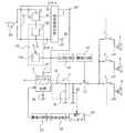
本発明の1実施形態は、デジタルアンプに本発明を実施したものである。このデジタルアンプは、図1に示すようにデジタルアンプ回路2を有している。デジタルアンプ回路2は、アナログ入力信号をパルス幅変調器やパルス密度変調器においてキャリア信号を用いてパルス幅変調信号またはパルス密度信号(以下、デジタル信号と称する。)に変換し、このデジタル信号をD級増幅方式による増幅器で電力増幅する。この増幅されたデジタル信号は、第1フィルタまたはローパス出力フィルタ、例えばLC出力フィルタ4によってデジタル信号に含まれるキャリア信号成分が除去されて、出力アナログ信号に変換されている。LC出力フィルタ4は、インダクタ4L及びコンデンサ4cの直列回路からなる。
One embodiment of the present invention is an implementation of the present invention in a digital amplifier. This digital amplifier has a
LC出力フィルタ4からの出力アナログ信号は、並列に接続された複数のスピーカ6に供給されている。これらスピーカは、ハイインピーダンス型のもので、ビルや店舗等における異なる位置に配置されている。出力アナログ信号は、これらスピーカ6に直列に接続されているスイッチ7が閉じられたものに供給される。各スイッチ7のうち図示しない制御回路から制御信号が供給されたものが閉じられる。または、スピーカ設置先のアッテネータ(減衰器)により音量が調整されることが多い。つまり、パワーアンプの負荷が頻繁に変化する。
The output analog signal from the
デジタルアンプ回路2を動作させるための直流電圧が、交流−直流変換手段、例えば直流電源回路8によって生成されている。即ち、直流電源回路8は、出力端子8P、8Nを有し、出力端子8Pがデジタルアンプ回路2の正電源端子2Pに接続され、出力端子8N及びデジタルアンプ回路2の負電源端子2Nが基準電位、例えば接地電位に接続されている。
A DC voltage for operating the
直流電源回路8は、2つの入力端子2IN−1、2IN−2を有し、これらは、商用交流電源入力端子、例えばコンセント10を介して商用交流電源(図示せず)に接続状態または非接続状態にされる。商用交流電源は、例えば実効値が100Vで、商用交流周波数が50Hzまたは60Hzのものである。
The DC power supply circuit 8 has two input terminals 2IN-1 and 2IN-2, which are connected or disconnected to a commercial AC power supply (not shown) via a commercial AC power supply input terminal, for example, an
直流電源回路8は、例えばスイッチング電源で、入力端子2IN−1、2IN−2に供給された商用交流電圧を整流する整流手段、例えば全波整流回路または半波整流回路によって整流し、この整流電圧を平滑手段、例えば平滑コンデンサで平滑する。この平滑電圧は、例えばチョッパ回路またはインバータ回路のようなスイッチング回路によって高周波電圧に変換され、絶縁トランスの一次巻線に供給される。絶縁トランスの二次巻線に誘起された高周波電圧が出力側整流平滑手段、例えば整流ダイオードによって整流され、かつ平滑リアクトルまたは平滑コンデンサによって平滑され、2つの出力端子8P、8N間に直流電圧を発生する。
The DC power supply circuit 8 is a switching power supply, for example, and rectifies the commercial AC voltage supplied to the input terminals 2IN-1 and 2IN-2 by a rectifier, for example, a full-wave rectifier circuit or a half-wave rectifier circuit. Is smoothed by a smoothing means such as a smoothing capacitor. This smoothed voltage is converted into a high frequency voltage by a switching circuit such as a chopper circuit or an inverter circuit, and supplied to the primary winding of the insulation transformer. The high frequency voltage induced in the secondary winding of the isolation transformer is rectified by an output side rectifying / smoothing means, for example, a rectifying diode, and smoothed by a smoothing reactor or a smoothing capacitor to generate a DC voltage between the two
直流電源回路8は、出力端子8P、8Nの他に基準電位端子8Rを持ち、出力端子8Pが基準電位端子8Rよりも正で、出力端子8Nが基準電位端子8Rよりも負の電圧を発生するように構成することもできる。なお、コンセント10の両端間、即ち直流電源回路8の入力端子2IN−1、2IN−2間には、第1のコンデンサ、例えば雑音除去用コンデンサ24が接続されている。
The DC power supply circuit 8 has a reference potential terminal 8R in addition to the
LC出力フィルタ4と各スピーカ6のスイッチ7との間には、開閉接点、例えばリレー開閉接点12が配置されている。リレー開閉接点12は通常には閉じられており、駆動回路14から駆動信号が供給されたとき、開放される。駆動回路14は、後述するように、コンセント10が商用交流電源と非接続状態になったとき、瞬時にリレー開閉接点12を開いて、デジタルアンプ回路2に供給される電圧の変動に基づく異音の発生を防止するためのものである。リレー開閉接点12と駆動回路14とが、保護回路、例えば出力側保護回路を構成している。
An open / close contact, for example, a relay open /
出力側保護回路を動作させるために、検出手段、例えば検出回路16が設けられている。検出回路16は、一次側と二次側を有し、両者が絶縁されたもので、例えばホトカプラーから構成されている。即ち、検出回路16は、一次側に発光素子、例えば発光ダイオード16Lを、二次側に受光素子、例えばホトトランジスタ16Pを有している。コンセント10が商用交流電源に接続されている状態では、発光ダイオード16Lが発光し、ホトトランジスタ16Pが受光信号を発生している。コンセント10が商用電源に非接続となると、ホトトランジスタ16Pが受光信号を発生しなくなる。これによって、比較回路18が駆動回路14に付勢信号を送り、駆動回路14が接点12を開放する。
In order to operate the output side protection circuit, detection means, for example, a
なお、ホトカプラー16には、交流入力対応型のものを使用することができる。この場合、2つの発光ダイオードが逆並列に接続されているので、付加回路は不要である。また、標準型のものを使用する場合、付加回路として発光ダイオードに逆並列にダイオードを接続する。
As the
発光ダイオード16Lは、フィルタ手段、例えばハイパスフィルタ21を介してコンセント10に接続されている。ハイパスフィルタ21は、抵抗手段、例えば抵抗回路網20と第2のコンデンサ、例えばコンデンサ22の直列回路によって構成されている。このハイパスフィルタ21のカット周波数は、商用交流電源の周波数よりも幾分低い周波数、例えば50Hzよりも幾分低い周波数に設定されている。
The
抵抗回路網20は、本来、発光ダイオード16Lの電流制限用に設けられており、図2に示すように、複数、例えば2つの並列回路20a、20bの直列回路によって構成されている。並列回路20aの2つの抵抗器は、予め定めた値、例えば68kΩのチップ型である。並列回路20bは、3つのチップ型抵抗器を並列に接続可能なものである。並列回路20bは、全ての抵抗器を取り外し、1つの抵抗器の接続端間をジャンパー線で短絡した状態としたり、2つの抵抗器に例えば68kΩの抵抗器を使用し、かつ残りの1つの抵抗器を除去したり、2つの抵抗器に例えば150kΩの抵抗器を使用し、かつ残りの1つの抵抗器を除去したりすることが可能である。
The
このように並列回路20bの構成を変更することによって、このデジタルアンプが、日本以外の地域でも使用される場合に、例えば米国のような商用交流電源の電圧が120Vであって周波数が60Hzの地域で使用される場合にも、欧州のような商用交流電源の電圧が230Vであって周波数が50Hzの地域で使用される場合にも、発光ダイオード16Lに流れる電流を所定の電流に制限することができる。また、どのような地域で使用される場合でも、コンデンサ22と共に構成しているハイパスフィルタ21のカット周波数を50Hzよりも幾分低い周波数に設定することができる。しかも、この構成の変更は、ごく容易に行える。
By changing the configuration of the
図2に示すように比較回路18は、ホトトランジスタ16Pのコレクタに抵抗器26を介して制御電極、例えばベースが接続されたスイッチング素子、例えばPNPトランジスタ28を有している。ホトトランジスタ16Pのエミッタは基準電位点、例えば接地電位に接続され、コレクタは抵抗器30を介して電源端子+Vに接続されている。電源端子+Vの電圧は、直流電源回路8の出力電圧より得られている。トランジスタ28の共通電極、例えばエミッタは電源端子+Vに接続され、出力電極、例えばコレクタは、抵抗器32を介して感度調整回路34に接続されている。感度調整回路34は、コンデンサ36と抵抗器38とを並列に接続した時定数回路で、抵抗器32のコレクタとは反対側の端部と接地電位との間に接続されている。この並列回路34の抵抗器38の接地側と反対側の端部が抵抗器40を介してスイッチング素子、例えばNPNトランジスタ42の制御電極、例えばベースに接続され、共通電極、例えばエミッタが接地されている。従って、感度調整回路34の出力電圧がベースに供給されている。トランジスタ42のコレクタは抵抗器44を介して電源端子+Vに接続されている。図示していないが、駆動回路14の動作電圧も+V端子から供給されている。
As shown in FIG. 2, the
ハイパスフィルタ21のカットオフ周波数は、商用交流電源の周波数よりも低いので、コンセント10が商用交流電源に接続されているとき、商用交流電圧がハイパスフィルタ21を介して発光ダイオード16に供給される。その結果、発光ダイオード16Lが発光し、ホトトランジスタ16Pが導通している。これによって、トランジスタ28、42が共に導通し、駆動回路14の入力側電圧は接地電位であり、接点12は閉じられたままである。このとき、感度調整回路34のコンデンサは、充電されている。また、コンデンサ24は、商用交流電圧によって充放電が繰り返されている。
Since the cutoff frequency of the high-
この状態において、コンセント10が商用交流電源と非接続状態になると、発光ダイオード16Lの発光が停止し、ホトトランジスタ16Pが非導通になる。これによって、トランジスタ28も非導通になり、コンデンサ34が放電を開始する。この放電電圧が、トランジスタ42の導通を維持するためにベース・エミッタ間に印加する必要のある電圧(基準電圧)よりも低下すると、トランジスタ42が非導通となり、+V端子の電圧が付勢信号として駆動回路14に供給され、駆動回路14が接点12を開放する。なお、感度調整回路34を設けたのは、瞬間的に商用交流電源の不具合により瞬間的に停電して、直ちに復電したような場合に、接点12が開放されることを防止するためである。
In this state, when the
上記の説明は、コンセント10が商用交流電源と非接続状態になると、発光ダイオード16Lの発光が直ちに停止すると仮定した場合である。しかし、実際には、コンセント10の両端には雑音抑制用のコンデンサ24が接続されているので、発光ダイオード16Lの発光は直ちに停止しない。
The above description is a case where it is assumed that when the
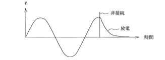
即ち、コンセント10が商用交流電源に接続されているとき、このコンデンサ24の充放電が繰り返されている。従って、コンセント10が商用交流電源と非接続になったとき、コンデンサ24は、正または負の或る電圧に充電されており、その電圧から放電が開始される。図3にコンデンサ24が正のピーク電圧に充電された状態で、商用交流電源にコンセント10が非接続とされ、コンデンサ24から放電が開始された状態を示す。この放電による放電電流が緩やかに発光ダイオード16Lに流れ続け、発光は直ちに停止せず、接点12が閉じられたままの状態が維持される。そのため直流電源回路8の出力電圧の低下に伴い、異音をスピーカ6から発生する可能性が高い。
That is, when the
ところで、この放電電流の周波数は、商用交流電源の周波数よりも低い。従って、コンデンサ22と抵抗回路網20とによって構成されたハイパスフィルタ21のカットオフ周波数の方が放電電流の周波数よりも高いので、ハイパスフィルタ21が、発光ダイオード16Lに放電電流が流れるのを急速に遮断し、発光ダイオード16Lの発光を急速に停止させる。コンセント10が非接続状態になると、+V端子の電圧も直流電源回路8内の平滑コンデンサ等の放電によって低下しているが、+V端子の電圧が比較回路18や駆動回路14を正常に動作させることができる電圧を維持している間に、発光ダイオード16Lが発光を停止し、接点12が開かれる。よって、異音がスピーカ6から出力されることはない。
By the way, the frequency of the discharge current is lower than the frequency of the commercial AC power supply. Accordingly, since the cutoff frequency of the high-
図1に戻って、LC出力フィルタ4は、デジタルアンプ回路2から出力されるデジタル信号をアナログ信号に変換する、即ち、デジタルアンプ回路2から出力されるキャリア信号を含んだ波形からキャリア信号を除去するためのローパスフィルタである。このLC出力フィルタ4のカットオフ周波数は、デジタルアンプ回路2の変調器におけるキャリア周波数、例えば350Hz以下であって、このデジタルアンプの品質保証帯域、例えば20Hz乃至20kHzの帯域の上限周波数である20kHzよりも高く設定されている。
Returning to FIG. 1, the
ところで、デジタルアンプ回路2に入力されるアナログ信号またはデジタルアンプ回路2内で増幅されたアナログ信号が過大となることがある。この場合、デジタルアンプ回路2から出力されるデジタル信号が歪む。この歪んだデジタル信号は様々な高調波成分を含み、LC出力フィルタ4の共振周波数及びその近傍の周波数成分を含むことがある。この場合、LC出力フィルタ4には大きな電流が流れる。そのため、デジタルアンプ回路2や直流電源回路8が破損する可能性がある。
Incidentally, an analog signal input to the
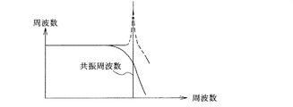
LC出力フィルタ4は、各スイッチ7が全て閉じられて、全てのハイインピーダンス型のスピーカ6がLC出力フィルタ4に接続されている際、所定の負荷インピーダンスとなり、図4に実線で示すようなローパスフィルタ特性を示す。しかし、各スピーカ6のうちスイッチ7が閉じられているものの数は常に一定ではなく、種々に変更されている。または、スピーカ設置先のアッテネータによって個別に音量調整されることもある。従って、LC出力フィルタ4に接続されているスピーカ6の数によって負荷インピーダンスが変化し、特にLC出力フィルタ4に接続されているスピーカ6の数が少ないときには、即ち、軽負荷のときには、LC出力フィルタ4は、図4に破線で示すように共振周波数において鋭いピークを発生する。この状態において、LC出力フィルタ4を流れる電流に共振周波数成分が含まれていると、共振電流が流れ、かつ共振電圧が発生する。特に、ハイインピーダンス型のスピーカ6が使用されている場合、各スピーカ6の定格出力電圧は日本で100V、米国では70Vと高圧であるので、LC出力フィルタ4に流れる共振電流は過大で、共振電圧も過大となる。従って、LC出力フィルタ4、デジタルアンプ回路2、直流電源回路8、接続されているスピーカが過大電圧による定格オーバーとなり、損傷する可能性が高い。
The
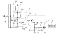
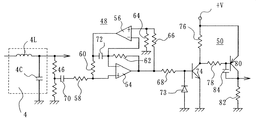
そこで、図5に示すようにLC出力フィルタ4のコンデンサ4Cの両端間電圧を分圧回路、例えば抵抗分圧回路46によって分圧した電圧が、第2フィルタまたは検出フィルタ、例えばバンドパスフィルタ48に供給される。なお、抵抗分圧回路46を構成する2つの直列接続抵抗器には、抵抗値の大きいものを使用し、LC出力フィルタ4の周波数特性に影響を与えないようにしてある。このバンドパスフィルタ48は、LC出力フィルタ4の共振周波数よりも幾分低い周波数付近にピークを持つ、例えば図6に示すようにQピークを持つものである。このバンドパスフィルタ48の出力電圧が、共振電流検出手段、例えば比較回路50に供給され、LC出力フィルタ4に共振電流が流れている場合、比較回路50が共振検出信号、例えば付勢信号を発生する。これに応動して、駆動回路52が、デジタルアンプ回路2内に設けられた信号減衰手段、例えばミュート回路(図示せず)を作動させて、デジタルアンプ回路2から歪んだデジタル信号が出力されることを阻止している。これによって、デジタルアンプ回路2や直流電源回路8に過大な電流が流れて、これらが破損することを防止している。比較回路50、駆動回路52及びミュート回路によって保護回路、或いは入力側保護回路が構成されている。
Therefore, as shown in FIG. 5, the voltage obtained by dividing the voltage across the
バンドパスフィルタ48は、図5に示すように2つの演算増幅器54、56、抵抗器58、60、62、64、66、68、コンデンサ70、72から構成され、図6に示すように、LC出力フィルタ4の共振周波数、例えば41kHzよりも幾分低い周波数にQピークを持つもので、そのゲインは、デジタルアンプ回路2の品質保証周波数帯の下限周波数、例えば20Hz付近では最もゲインが負の値であり、周波数が高くなるに従ってゲインが徐々に増加する。但し、品質保証周波数帯の上限周波数、例えば20kHz付近でもまだ負のゲインであり、Qピーク周波数よりも幾分低い周波数でゲインが正となり、Qピーク周波数で最大ゲインとなる。以後、ゲインは周波数が高くなると低下するが、それでも負のゲインとなることはなく、デジタルアンプ回路2のキャリア周波数350kHzを超えても正の一定ゲインを有するように構成されている。なお、図示していない高い周波数領域において、ゲインは負の値となる。このようにLC出力フィルタ4の共振周波数よりも幾分低い周波数よりも高い周波数成分がLC出力フィルタ4に生じているとき、その成分の電圧よりも大きい電圧が出力電圧としてバンドパスフィルタ48に生じる。
The band-
比較回路50は、抵抗器68及びダイオード69を介して制御電極、例えばベースにバンドパスフィルタ48の出力電圧が供給される半導体スイッチング素子、例えばNPNトランジスタ74を有し、その共通電極、例えばエミッタが基準電位、例えば接地電位に接続されている。出力電極、例えばコレクタは、抵抗器76を介して+V端子に接続されている。トランジスタ74のコレクタは抵抗器78を介して半導体スイッチング素子、例えばPNPトランジスタ80の制御電極、例えばベースに接続されている。このトランジスタ80のエミッタに接続されている。また、出力電極、例えばコレクタは抵抗器82を介して接地電位に接続され、かつ駆動回路52に接続されている。また、ベースとコレクタとの間にはコンデンサ84が接続されている。このコンデンサ84と抵抗器78とによって感度調整器が構成されている。
The
デジタルアンプ回路2への入力信号のレベルが低く、デジタルアンプ回路2の出力信号が歪んでいない状態や、周波数がLC出力フィルタの共振周波数より離れているときは、LC出力フィルタ4に共振電流が流れていない。そのため、バンドパスフィルタ48の出力電圧はその入力電圧よりも低く、トランジスタ74を導通させるために必要なベース・エミッタ間電圧がトランジスタ74のベース・エミッタ間には供給されて無く、トランジスタ74は非導通である。そのため、トランジスタ80を導通させるために必要なベース・エミッタ間電圧もトランジスタ80のベース・エミッタ間にも得られず、トランジスタ80も非導通である。よって、駆動回路52には接地電位の電圧が供給されており、駆動回路52は作動していない。このとき、コンデンサ84は充電されている。
When the level of the input signal to the
デジタルアンプ回路2への入力信号のレベルが高く、デジタルアンプ回路2の出力波形が歪んだ状態や、周波数がLC出力フィルタの共振周波数に近いときは、LC出力フィルタ4に大きな共振電流が流れる。これによって、バンドパスフィルタ48の出力電圧がその入力電圧よりも大きくなる。トランジスタ74が導通し、コンデンサ84が急速に放電して、トランジスタ80が導通し、+V端子の電圧が付勢信号として駆動回路52に供給される。デジタルアンプ回路2内のミュート回路が作動し、デジタルアンプ回路2での歪んだ出力信号の発生が停止する。これによって、共振電流がLC出力フィルタ4に流れなくなり、LC出力フィルタ4、デジタルアンプ回路2、直流電源回路8の破損を防止することができる。なお、バンドパスフィルタ84の出力電圧が低下して、トランジスタ74が非導通になっても、コンデンサ84が充電されている期間中、トランジスタ80の導通状態が維持され、ミュート回路の動作が継続される。
When the level of the input signal to the
このようにバンドパスフィルタ84は、LC出力フィルタ4のコンデンサ4Cに直列には接続されずに、分圧回路46を介してコンデンサ4Cの電圧を検出しているので、LC出力フィルタ4の特性に影響を与えることがなく、また、不要な高調波の放射を生じない。しかも、このバンドパスフィルタ84を使用することによって、コンデンサ4Cを流れている共振電流を実質的に検出することができる。
As described above, the
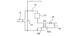
第2の実施形態を図7に示す。この実施形態では、ホトカプラー16に代えて一次巻線86Pと二次巻線86Sとが絶縁されている変圧器86を使用したものである。一次巻線86Pは、抵抗回路網20と直列に接続されている。二次巻線86Sには、整流ダイオード88と平滑コンデンサ90とからなる整流・平滑回路92が接続されている。この平滑回路92の出力電圧が、比較回路18に供給される。他の構成は、第1の実施形態と同様である。
A second embodiment is shown in FIG. In this embodiment, a
上記の2つの実施形態では、デジタルアンプに本発明を実施したが、フィルタを備え、そのフィルタの共振周波数またはそれに近い周波数の電流が流れる可能性のある機器、例えばスイッチング電源としてのインバータやLC回路を用いた大電力無線機等に実施することもできる。上記の実施形態では、バンドパスフィルタ48を使用したが、これに限ったものではなく、LC出力フィルタ4の共振周波数よりも幾分低い周波数にQピークを持つハイパスフィルタを使用することもできる。また、上記の実施形態では、保護回路としてデジタルアンプ回路2内のミュート回路と駆動回路52とを使用したが、例えば直流電源回路8からデジタルアンプ回路2への電源供給を遮断する回路を保護回路として使用することもできる。また、LCフィルタを外付けで使用する汎用のデジタルICアンプに、上述したバンドパスフィルタ48及び比較回路50等からなる検出用の回路を追加することで、デジタルICアンプの本来の性能に影響を及ぼさないで容易に保護機能を追加することができる。また、上記の実施の形態では、バンドパスフィルタ48のQピーク周波数を、LC出力フィルタ4の共振周波数より幾分低い周波数としたが、共振周波数と一致させることもできる。
In the above two embodiments, the present invention is implemented in a digital amplifier. However, a device that includes a filter and that may flow a current at or near the resonance frequency of the filter, such as an inverter or an LC circuit as a switching power supply. It can also be implemented in a high-power radio device using the. In the above embodiment, the band-
2 デジタルアンプ回路
4 LC出力フィルタ(第1フィルタ、ローパス出力フィルタ)
48 バンドパスフィルタ(第2フィルタ、検出フィルタ)
50 比較回路(共振検出手段)
2
48 Bandpass filter (second filter, detection filter)
50 comparison circuit (resonance detection means)
Claims (2)
このデジタルアンプの出力側と前記スピーカとの間に設けられた、コンデンサとインダクタとからなるLCローパス出力フィルタと、
このLCローパス出力フィルタの出力電圧が供給され、前記LCローパス出力フィルタの共振周波数よりも幾分低い周波数で、ゲインが正となり、前記共振周波数よりも高い周波数でも正のゲインを有する検出フィルタと、
この検出フィルタの出力信号が供給され、前記検出フィルタが正のゲインを有しているとき動作して前記デジタルアンプを保護する保護回路とを、
具備するデジタルアンプの保護装置。 In digital amplifiers that have multiple high-impedance speakers and the number of connected speakers changes.
An LC low-pass output filter comprising a capacitor and an inductor, provided between the output side of the digital amplifier and the speaker;
An output voltage of the LC low-pass output filter is supplied , a detection filter having a positive gain at a frequency somewhat lower than the resonance frequency of the LC low-pass output filter, and a positive gain even at a frequency higher than the resonance frequency;
A protection circuit that operates when the output signal of the detection filter is supplied and the detection filter has a positive gain to protect the digital amplifier;
Protection device for digital amplifier.
Priority Applications (1)
| Application Number | Priority Date | Filing Date | Title |
|---|---|---|---|
| JP2006078728A JP4792308B2 (en) | 2006-03-22 | 2006-03-22 | Digital amplifier protector |
Applications Claiming Priority (1)
| Application Number | Priority Date | Filing Date | Title |
|---|---|---|---|
| JP2006078728A JP4792308B2 (en) | 2006-03-22 | 2006-03-22 | Digital amplifier protector |
Publications (2)
| Publication Number | Publication Date |
|---|---|
| JP2007258903A JP2007258903A (en) | 2007-10-04 |
| JP4792308B2 true JP4792308B2 (en) | 2011-10-12 |
Family
ID=38632720
Family Applications (1)
| Application Number | Title | Priority Date | Filing Date |
|---|---|---|---|
| JP2006078728A Expired - Lifetime JP4792308B2 (en) | 2006-03-22 | 2006-03-22 | Digital amplifier protector |
Country Status (1)
| Country | Link |
|---|---|
| JP (1) | JP4792308B2 (en) |
Families Citing this family (3)
| Publication number | Priority date | Publication date | Assignee | Title |
|---|---|---|---|---|
| JP5430438B2 (en) * | 2010-02-18 | 2014-02-26 | パナソニック株式会社 | Digital amplifier |
| JP5861442B2 (en) * | 2011-12-20 | 2016-02-16 | ヤマハ株式会社 | Class D power amplifier |
| WO2019069692A1 (en) * | 2017-10-04 | 2019-04-11 | ソニー株式会社 | Signal processing device, signal processing method, and program |
Family Cites Families (5)
| Publication number | Priority date | Publication date | Assignee | Title |
|---|---|---|---|---|
| JPH0617437Y2 (en) * | 1984-08-20 | 1994-05-02 | パイオニア株式会社 | Speaker switch for power amplifier |
| JP2808024B2 (en) * | 1989-11-17 | 1998-10-08 | 富士通テン株式会社 | Switching amplifier protection circuit |
| JP2005123949A (en) * | 2003-10-17 | 2005-05-12 | Yamaha Corp | Class d amplifier |
| JP2005203968A (en) * | 2004-01-14 | 2005-07-28 | Denon Ltd | Protective device for digital amplifier |
| WO2006028054A1 (en) * | 2004-09-08 | 2006-03-16 | Pioneer Corporation | Class d amplifier |
-
2006
- 2006-03-22 JP JP2006078728A patent/JP4792308B2/en not_active Expired - Lifetime
Also Published As
| Publication number | Publication date |
|---|---|
| JP2007258903A (en) | 2007-10-04 |
Similar Documents
| Publication | Publication Date | Title |
|---|---|---|
| US7667988B2 (en) | Filter | |
| JP2017063607A (en) | Ac power supply (ac) direct coupling lamp including leakage current protection circuit | |
| CN104659742B (en) | A kind of residual current device | |
| US20220091172A1 (en) | Arc Fault Detection Device with Wideband Sensor | |
| JP2008228538A (en) | Switching power supply | |
| WO2013088635A1 (en) | High output power amplifier | |
| US6201680B1 (en) | Adjustable high-speed audio transducer protection circuit | |
| CN111566885A (en) | Circuit arrangements for combined protection of loads against temporary and transient overvoltages | |
| US6721151B2 (en) | Ground fault interrupter | |
| JP4916478B2 (en) | Audio amplifier | |
| JP4792308B2 (en) | Digital amplifier protector | |
| JP2007288995A (en) | Device for detecting disconnection from power source and device for protecting electronic apparatus | |
| KR100933533B1 (en) | Electromagnetic interference prevention device of earth leakage breaker | |
| JP2002315201A (en) | Discharge prevention circuit | |
| US10637457B2 (en) | Method and device for controlling a semiconductor switch | |
| CN116505480A (en) | Residual current device for protecting an electrical device from alternating and/or direct current | |
| US20210006235A1 (en) | Compensation Filter and Method for Activating a Compensation Filter | |
| KR101033699B1 (en) | High frequency malfunction prevention circuit of earth leakage breaker | |
| JP5109243B2 (en) | Short detection circuit | |
| JP2002101505A (en) | switchboard | |
| CN107635299B (en) | Electromagnetic heating cooking system and driving chip of power switch tube thereof | |
| CN105849850A (en) | Breaker | |
| JP2012182956A (en) | Power supply circuit | |
| US10310001B2 (en) | Short-circuit sensor | |
| JP4916477B2 (en) | Audio amplifier |
Legal Events
| Date | Code | Title | Description |
|---|---|---|---|
| A621 | Written request for application examination |
Free format text: JAPANESE INTERMEDIATE CODE: A621 Effective date: 20071203 |
|
| A977 | Report on retrieval |
Free format text: JAPANESE INTERMEDIATE CODE: A971007 Effective date: 20100129 |
|
| A131 | Notification of reasons for refusal |
Free format text: JAPANESE INTERMEDIATE CODE: A131 Effective date: 20100202 |
|
| A521 | Request for written amendment filed |
Free format text: JAPANESE INTERMEDIATE CODE: A523 Effective date: 20100330 |
|
| A131 | Notification of reasons for refusal |
Free format text: JAPANESE INTERMEDIATE CODE: A131 Effective date: 20101019 |
|
| A521 | Request for written amendment filed |
Free format text: JAPANESE INTERMEDIATE CODE: A523 Effective date: 20101217 |
|
| TRDD | Decision of grant or rejection written | ||
| A01 | Written decision to grant a patent or to grant a registration (utility model) |
Free format text: JAPANESE INTERMEDIATE CODE: A01 Effective date: 20110719 |
|
| A01 | Written decision to grant a patent or to grant a registration (utility model) |
Free format text: JAPANESE INTERMEDIATE CODE: A01 |
|
| A61 | First payment of annual fees (during grant procedure) |
Free format text: JAPANESE INTERMEDIATE CODE: A61 Effective date: 20110725 |
|
| FPAY | Renewal fee payment (event date is renewal date of database) |
Free format text: PAYMENT UNTIL: 20140729 Year of fee payment: 3 |
|
| R150 | Certificate of patent or registration of utility model |
Ref document number: 4792308 Country of ref document: JP Free format text: JAPANESE INTERMEDIATE CODE: R150 Free format text: JAPANESE INTERMEDIATE CODE: R150 |
|
| FPAY | Renewal fee payment (event date is renewal date of database) |
Free format text: PAYMENT UNTIL: 20140729 Year of fee payment: 3 |
|
| S533 | Written request for registration of change of name |
Free format text: JAPANESE INTERMEDIATE CODE: R313533 |
|
| FPAY | Renewal fee payment (event date is renewal date of database) |
Free format text: PAYMENT UNTIL: 20140729 Year of fee payment: 3 |
|
| R350 | Written notification of registration of transfer |
Free format text: JAPANESE INTERMEDIATE CODE: R350 |
|
| R250 | Receipt of annual fees |
Free format text: JAPANESE INTERMEDIATE CODE: R250 |
|
| R250 | Receipt of annual fees |
Free format text: JAPANESE INTERMEDIATE CODE: R250 |
|
| R250 | Receipt of annual fees |
Free format text: JAPANESE INTERMEDIATE CODE: R250 |
|
| R250 | Receipt of annual fees |
Free format text: JAPANESE INTERMEDIATE CODE: R250 |
|
| R250 | Receipt of annual fees |
Free format text: JAPANESE INTERMEDIATE CODE: R250 |
|
| R250 | Receipt of annual fees |
Free format text: JAPANESE INTERMEDIATE CODE: R250 |
|
| R250 | Receipt of annual fees |
Free format text: JAPANESE INTERMEDIATE CODE: R250 |
|
| R250 | Receipt of annual fees |
Free format text: JAPANESE INTERMEDIATE CODE: R250 |
|
| R250 | Receipt of annual fees |
Free format text: JAPANESE INTERMEDIATE CODE: R250 |
|
| R250 | Receipt of annual fees |
Free format text: JAPANESE INTERMEDIATE CODE: R250 |
|
| R250 | Receipt of annual fees |
Free format text: JAPANESE INTERMEDIATE CODE: R250 |
|
| R250 | Receipt of annual fees |
Free format text: JAPANESE INTERMEDIATE CODE: R250 |