JP4792169B2 - Device for loading electronic components into its storage case - Google Patents
Device for loading electronic components into its storage case Download PDFInfo
- Publication number
- JP4792169B2 JP4792169B2 JP2001143180A JP2001143180A JP4792169B2 JP 4792169 B2 JP4792169 B2 JP 4792169B2 JP 2001143180 A JP2001143180 A JP 2001143180A JP 2001143180 A JP2001143180 A JP 2001143180A JP 4792169 B2 JP4792169 B2 JP 4792169B2
- Authority
- JP
- Japan
- Prior art keywords
- electronic component
- lead frame
- tunnel
- separated
- case
- Prior art date
- Legal status (The legal status is an assumption and is not a legal conclusion. Google has not performed a legal analysis and makes no representation as to the accuracy of the status listed.)
- Expired - Fee Related
Links
- 230000007246 mechanism Effects 0.000 description 4
- 238000005452 bending Methods 0.000 description 2
- 238000007796 conventional method Methods 0.000 description 1
- 238000004806 packaging method and process Methods 0.000 description 1
Images
Landscapes
- Photo Coupler, Interrupter, Optical-To-Optical Conversion Devices (AREA)
Description
【0001】
【発明の属する技術分野】
本発明は、各種の電子部品を、これを収容するケース内に装填するための装置に関するものである。
【0002】
【従来の技術】
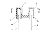
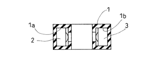
電子部品とこれを収容するケースとから成るケース入り電子部品の代表例であるところのホトインタラプターは、図1及び図2に示すように、合成樹脂製のケース1における二つの収容部1a,1b内に、少なくとも一対のリード端子2′を備えた発光素子2と、同じく少なくとも一対のリード端子3′を備えた受光素子3とを、互いに向かい合わせにして装填するという構成にしている(例えば、特開平7−94775号公報等参照)。
【0003】
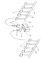
ところで、この構造のホトインタラプターにおいて使用される発光素子2及び受光素子3は、図3に示すように、リードフレームA,Bにより複数個ずつ製造される。
【0004】
そこで、従来、前記ホトインタラプターへの組み立てに際しては、リードフレームA,Bにて製造された発光素子2及び受光素子3の一つをリードフレームA,Bから切り離し、次いで、この一つの発光素子2及び受光素子3を下向きに方向変換したのち、上向き姿勢にしたケース1における両収容部1a,1b内に装填するという方法が採用されている。
【0005】
【発明が解決しようとする課題】
この組み立てにおいて従来は、発光素子2及び受光素子3をその各々のリードフレームA,Bより切り離すと、この発光素子2及び受光素子3におけるリード端子2′,3′の部分をクランプし、このクランプした状態で、下向きへの方向変換と、ケース1内への装填とを行うようにしているから、発光素子2及び受光素子3におけるリード端子2′,3′に曲がり変形が発生するおそれが大きいばかりか、装置の構造が複雑で、著しく大型で且つ高価になるという問題があった。
【0006】
本発明は、前記したように、リードフレームから切り離した電子部品を、上下逆向きに方向変換したのちケースに収容する場合に、前記したような問題が発生しないようにした装置を提供することを技術的課題とするものである。
【0007】
【課題を解決するための手段】
この技術的課題を達成するため本発明の請求項1は、
「リードフレームにおける電子部品をリードフレームから切り離す箇所と、前記電子部品を収容するケースとの間に、前記電子部品が通過するように構成したトンネルを、上向き略半円形状に湾曲して設け、このトンネルの両端のうち一端における下向き開口部を、前記リードフレームから切り離す電子部品の真上の部位に位置して、この下方に、当該一端の下向き開口部に対して空気を吹き込むようにしたノズルを設ける。」
という構成にした。
【0008】
また、本発明の請求項2は、
「第1リードフレームにおける電子部品を第1リードフレームから切り離す箇所と、第2リードフレームにおける電子部品を第2リードフレームから切り離す箇所との中間に、前記各電子部品を収容するケースを配設し、このケースと前記第1リードフレームとの間に、前記電子部品が通過するように構成した第1トンネルを、上向き略半円形状に湾曲して設け、この第1トンネルの両端のうち一端における下向き開口部を、前記第1リードフレームから切り離す電子部品の真上の部位に位置して、この下方に、当該一端の下向き開口部に対して空気を吹き込むようにしたノズルを設ける一方、前記ケースと前記第2リードフレームとの間に、前記電子部品が通過するように構成した第2トンネルを、上向き略半円形状に湾曲して設け、この第2トンネルの両端のうち一端における下向き開口部を、前記第2リードフレームから切り離す電子部品の真上の部位に位置して、この下方に、当該一端の下向き開口部に対して空気を吹き込むようにしたノズルを設ける。」
という構成にした。
【0009】
【発明の作用・効果】
この構成において、リードフレームから切り離された電子部品は、その下方におけるノズルから噴出する空気によって、トンネルの一端における下向き開口部に吹き込まれ、トンネル内を空気流にて通過するとき上下逆向きに方向変換し、そして、トンネルの他端における下向き開口部からケース内に装填される。
【0010】
つまり、本発明によると、リードフレームから切り離した電子部品を、逆向きに方向変換したのちケースに装填することを、当該電子部品におけるリード端子の部分をクランプすることなく行うことができるから、電子部品におけるリード端子に曲がり変形が発生することを大幅に低減できるとともに、装置の構造が著しく簡単になり、その小型化及び低価格化を確実に達成できる効果を有する。
【0011】
特に、請求項2のように構成した場合には、一つのケースに対して二つの電子部品を一挙に装填することができるので、前記例示したホトインタラプターの組み立てに適用して、多大の効果を発揮するのである。
【0012】
【発明の実施の形態】
以下、本発明の実施の形態を、前記例示したホトインタラプターの組み立てに適用した場合を示す図面(図4及び図5)について説明する。
【0013】
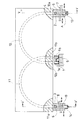
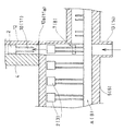
この図において、符号4は、鉛直に立設したトンネル用パネルを示し、このトンネル用パネル4における下面には、その一端部に、前記ホトインタラプターにおける発光素子2の複数個を備えた第1リードフレームAをその長手方向に移送するように保持する第1ホルダー5が、その他端部に、前記ホトインタラプターにおける受光素子3の複数個を備えた第2リードフレームBをその長手方向に移送するように保持する第2ホルダー6が各々配設され、これら両ホルダー5,6には、発光素子2及び受光素子3をその各々のリードフレームA,Bから切り離すためのカッター機構7,8が設けられている。
【0014】
更にまた、前記トンネル用パネル4における下面のうち前記両ホルダー5,6の中間の部位には、ホトインタラプターにおけるケース1を上向きの姿勢で一つずつ供給するための供給台9が設けられている。
【0015】
前記トンネル用パネル4の内部には、前記第1ホルダー5と前記供給台9との間に第1トンネル10を、前記第2ホルダー6と供給台9との間に第2トンネル11を、各々上向き半円形に湾曲して設けて、この両トンネル10,11のうち第1トンネル10においては、その一端の下向き開口部10aを、前記第1ホルダー5において第1リードフレームAより切り離した発光素子2の真上の部位に、他端の下向き開口部10bを、前記供給台9のケース1のうち発光素子用収容部1aの真上に各々位置するように構成する一方、前記両トンネル10,11のうち第2トンネル11においては、その一端の下向き開口部11aを、前記第2ホルダー6において第2リードフレームBより切り離した受光素子3の真上の部位に、他端の下向き開口部11bを、前記供給台9のケース1のうち受光素子用収容部1bの真上に各々位置するように構成する。
【0016】
なお、前記実施の形態は、第1トンネル10及び第2トンネル11を、トンネル用パネル4に刻設した溝をトンネル用パネル4の前面に取付けた蓋板12にて塞ぐことによって形成する場合を示したが、これに限らず、これら両トンネル10,11は、パイプを上向き半円形に湾曲変形することによって形成するようにしても良い。
【0017】
そして、前記第1ホルダー5には、第1トンネル10の一端における下向き開口部10aに対して空気を吹き込むようにしたノズル13を、前記第2ホルダー6には、第2トンネル11の一端における下向き開口部11aに対して空気を吹き込むようにしたノズル14を各々設ける。
【0018】
この構成において、第1ホルダー5において、第1リードフレームAから一つの発光素子2がカッター機構7にて切り離されると、この発光素子2は、その下方におけるノズル13から噴出する空気によって、第1トンネル10の一端における下向き開口部10aに吹き込まれ、第1トンネル10内を空気流にて通過するとき上下逆向きに方向変換し、そして、第1トンネル10の他端における下向き開口部10bからケース1における発光素子用収容部1a内に装填される。
【0019】
また、第2ホルダー6において、第2リードフレームBから一つの受光素子3がカッター機構8にて切り離されると、この受光素子3は、その下方におけるノズル14から噴出する空気によって、第2トンネル11の一端における下向き開口部11aに吹き込まれ、第2トンネル11内を空気流にて通過するとき上下逆向きに方向変換し、そして、第2トンネル11の他端における下向き開口部11bからケース1における受光素子用収容部1b内に装填される。
【0020】
このようにして一つのケース1内に発光素子2と受光素子3とを装填すると、供給台9に空のケース1を供給する一方、第1リードフレームA及び第2リードフレームBを一ピッチ送り、以後、前記のことを繰り返すのである。
【0021】
なお、前記第1トンネル10と第2トンネル11とは、図示のように、供給台9側の部分において互いに交差するように構成しても良いが、交差しないように構成することができる。
【0022】
このように、両トンネル10,11を交差しないように構成した場合には、一つのケース1に対する発光素子2及び受光素子3の装填を同時に行うことができるから、速度を早くできる。
【0023】
また、前記各トンネル10,11を、その途中を軸線の回りに捩じった螺旋状トンネルに構成することにより、電子部品を、当該トンネル内の通過するときにその軸線の回りに方向変換することができる。
【0024】
更にまた、本発明は、前記実施の形態のようにホトインタラプターの組み立てに適用することに限らず、リードフレームにおける各電子部品を、その包装用のケースに収容する場合にも適用できることはいうまでもない。
【図面の簡単な説明】
【図1】ホトインタラプターの縦断正面図である。
【図2】図1のII−II視断面図である。
【図3】従来の方法によるホトインタラプターの組み立てを示す斜視図である。
【図4】本発明の実施の形態を示す一部切欠正面図である。
【図5】図4のV−V、V′−V′視拡大断面図である。
【符号の説明】
1 ホトインタラプターのケース
2 発光素子
3 受光素子
2′,3′ リード
A,B リードフレーム
4 トンネル用パネル
5,6 ホルダー
7,8 カッター機構
9 供給台
10,11 トンネル[0001]
BACKGROUND OF THE INVENTION
The present invention relates to an apparatus for loading various electronic components in a case that accommodates the electronic components.
[0002]
[Prior art]
As shown in FIGS. 1 and 2, the photo interrupter, which is a representative example of a cased electronic component composed of an electronic component and a case for accommodating the electronic component, includes two
[0003]
By the way, a plurality of
[0004]
Therefore, conventionally, when assembling the photo interrupter, one of the
[0005]
[Problems to be solved by the invention]
Conventionally, in this assembly, when the
[0006]
As described above, the present invention provides an apparatus in which the above-described problem does not occur when an electronic component separated from a lead frame is accommodated in a case after the direction is changed in the upside down direction. It is a technical issue.
[0007]
[Means for Solving the Problems]
In order to achieve this technical problem,
“A tunnel configured to allow the electronic component to pass between a portion where the electronic component in the lead frame is separated from the lead frame and a case for housing the electronic component is curved in a substantially semicircular shape upward, A nozzle in which a downward opening at one end of the tunnel is located at a position directly above an electronic component to be separated from the lead frame, and below this, a nozzle is configured to blow air into the downward opening of the one end. Is provided. "
It was configured as follows.
[0008]
Further,
“A case for housing each electronic component is disposed between a location where the electronic component in the first lead frame is separated from the first lead frame and a location where the electronic component in the second lead frame is separated from the second lead frame. A first tunnel configured to allow the electronic component to pass therethrough is provided between the case and the first lead frame so as to be curved in a substantially semicircular shape upward, and at one end of both ends of the first tunnel. While the downward opening is located at a position directly above the electronic component to be separated from the first lead frame, a nozzle is provided below the nozzle so as to blow air into the downward opening of the one end. And a second tunnel configured to allow the electronic component to pass between the second lead frame and the second lead frame. The downward opening at one end of the two tunnels is located at a position directly above the electronic component to be separated from the second lead frame, and air is blown into the downward opening at the one end below this Provide a nozzle. "
It was configured as follows.
[0009]
[Operation and effect of the invention]
In this configuration, the electronic component cut off from the lead frame is blown into the downward opening at one end of the tunnel by the air jetted from the nozzle below it, and is directed in the upside down direction when passing through the tunnel by the air flow. Converted and loaded into the case from the downward opening at the other end of the tunnel.
[0010]
In other words, according to the present invention, the electronic component separated from the lead frame can be loaded in the case after changing the direction in the opposite direction without clamping the lead terminal portion of the electronic component. It is possible to greatly reduce the occurrence of bending deformation in the lead terminals of the components, and the structure of the device is remarkably simplified, and the miniaturization and the cost reduction can be reliably achieved.
[0011]
In particular, when configured as in
[0012]
DETAILED DESCRIPTION OF THE INVENTION
Hereinafter, drawings (FIGS. 4 and 5) illustrating a case where an embodiment of the present invention is applied to the assembly of the illustrated photo interrupter will be described.
[0013]
In this figure,
[0014]
Furthermore, a
[0015]
Inside the
[0016]
In the embodiment described above, the
[0017]
The
[0018]
In this configuration, in the
[0019]
Further, in the
[0020]
When the
[0021]
In addition, although the said
[0022]
As described above, when the two
[0023]
Further, the
[0024]
Furthermore, the present invention is not limited to application to the assembly of a photo interrupter as in the above-described embodiment, but can also be applied to the case where each electronic component in the lead frame is accommodated in its packaging case. Not too long.
[Brief description of the drawings]
FIG. 1 is a longitudinal front view of a photo interrupter.
2 is a cross-sectional view taken along the line II-II of FIG.
FIG. 3 is a perspective view showing assembly of a photo interrupter according to a conventional method.
FIG. 4 is a partially cutaway front view showing an embodiment of the present invention.
5 is an enlarged sectional view taken along line VV and V′-V ′ in FIG. 4;
[Explanation of symbols]
DESCRIPTION OF
Claims (2)
Priority Applications (1)
| Application Number | Priority Date | Filing Date | Title |
|---|---|---|---|
| JP2001143180A JP4792169B2 (en) | 2001-05-14 | 2001-05-14 | Device for loading electronic components into its storage case |
Applications Claiming Priority (1)
| Application Number | Priority Date | Filing Date | Title |
|---|---|---|---|
| JP2001143180A JP4792169B2 (en) | 2001-05-14 | 2001-05-14 | Device for loading electronic components into its storage case |
Publications (2)
| Publication Number | Publication Date |
|---|---|
| JP2002344007A JP2002344007A (en) | 2002-11-29 |
| JP4792169B2 true JP4792169B2 (en) | 2011-10-12 |
Family
ID=18989362
Family Applications (1)
| Application Number | Title | Priority Date | Filing Date |
|---|---|---|---|
| JP2001143180A Expired - Fee Related JP4792169B2 (en) | 2001-05-14 | 2001-05-14 | Device for loading electronic components into its storage case |
Country Status (1)
| Country | Link |
|---|---|
| JP (1) | JP4792169B2 (en) |
-
2001
- 2001-05-14 JP JP2001143180A patent/JP4792169B2/en not_active Expired - Fee Related
Also Published As
| Publication number | Publication date |
|---|---|
| JP2002344007A (en) | 2002-11-29 |
Similar Documents
| Publication | Publication Date | Title |
|---|---|---|
| JP4776483B2 (en) | Connector mounting structure | |
| CN102947060B (en) | Gripping device | |
| CN107388547B (en) | Air deflector driving device for air conditioner indoor unit and air conditioner indoor unit | |
| JP4792169B2 (en) | Device for loading electronic components into its storage case | |
| US20250020882A1 (en) | Cable Organizing Mechanism, Cable Arranging Mechanism, Connecting Plate for Cable Distribution and Cable Distribution Rack | |
| CN1097489C (en) | Masking apparatus for coating | |
| US6863206B2 (en) | Bonding apparatus | |
| JP7028134B2 (en) | How to assemble connectors for electronic components, assembly jigs, assembly equipment | |
| JP2007053848A (en) | Wiring board assembly, wiring structure, and wiring method | |
| JPS58154253A (en) | Ic lead reforming mechanism | |
| JP4243169B2 (en) | Punching device | |
| JP2755343B2 (en) | Material handling equipment for manufacturing electronic components | |
| KR200258966Y1 (en) | Air sensor assembly | |
| JP2005342732A (en) | Cable holding device | |
| JP2505924B2 (en) | Method and apparatus for manufacturing interconnect assembly | |
| JPH0939662A (en) | Outside mirror for automobile | |
| JP3282367B2 (en) | Wire bonding equipment | |
| KR950005793Y1 (en) | Arranging device to load work-piece | |
| CN101625989A (en) | Wire feeding/drawing device and method thereof | |
| EP0080030A1 (en) | Television receiver with a chassis a base for printed circuits whose form corresponds to the form of the cathodic tube | |
| KR200246932Y1 (en) | Adsorption nozzle for mounter | |
| JP2008130649A (en) | Transmission type photo interrupter and manufacturing method thereof | |
| JP3829762B2 (en) | Cable holder and flat cable folding method using the same | |
| JP2005104588A (en) | Ring lamp case holder and packing device using the same | |
| JP3244358B2 (en) | Linear light source |
Legal Events
| Date | Code | Title | Description |
|---|---|---|---|
| A621 | Written request for application examination |
Free format text: JAPANESE INTERMEDIATE CODE: A621 Effective date: 20080514 |
|
| A977 | Report on retrieval |
Free format text: JAPANESE INTERMEDIATE CODE: A971007 Effective date: 20110624 |
|
| TRDD | Decision of grant or rejection written | ||
| A01 | Written decision to grant a patent or to grant a registration (utility model) |
Free format text: JAPANESE INTERMEDIATE CODE: A01 Effective date: 20110629 |
|
| A01 | Written decision to grant a patent or to grant a registration (utility model) |
Free format text: JAPANESE INTERMEDIATE CODE: A01 |
|
| A61 | First payment of annual fees (during grant procedure) |
Free format text: JAPANESE INTERMEDIATE CODE: A61 Effective date: 20110725 |
|
| FPAY | Renewal fee payment (prs date is renewal date of database) |
Free format text: PAYMENT UNTIL: 20140729 Year of fee payment: 3 |
|
| R150 | Certificate of patent (=grant) or registration of utility model |
Free format text: JAPANESE INTERMEDIATE CODE: R150 |
|
| LAPS | Cancellation because of no payment of annual fees |