JP4786924B2 - Photonic mixer device - Google Patents
Photonic mixer device Download PDFInfo
- Publication number
- JP4786924B2 JP4786924B2 JP2005107084A JP2005107084A JP4786924B2 JP 4786924 B2 JP4786924 B2 JP 4786924B2 JP 2005107084 A JP2005107084 A JP 2005107084A JP 2005107084 A JP2005107084 A JP 2005107084A JP 4786924 B2 JP4786924 B2 JP 4786924B2
- Authority
- JP
- Japan
- Prior art keywords
- mixer device
- photonic mixer
- electrode
- readout
- modulation
- Prior art date
- Legal status (The legal status is an assumption and is not a legal conclusion. Google has not performed a legal analysis and makes no representation as to the accuracy of the status listed.)
- Active
Links
- 238000000926 separation method Methods 0.000 claims description 27
- 239000004065 semiconductor Substances 0.000 claims description 20
- 230000005670 electromagnetic radiation Effects 0.000 claims description 19
- 239000000463 material Substances 0.000 claims description 19
- 229910052751 metal Inorganic materials 0.000 claims description 10
- 239000002184 metal Substances 0.000 claims description 10
- 230000006870 function Effects 0.000 claims description 8
- VYPSYNLAJGMNEJ-UHFFFAOYSA-N Silicium dioxide Chemical compound O=[Si]=O VYPSYNLAJGMNEJ-UHFFFAOYSA-N 0.000 claims description 4
- 229910052814 silicon oxide Inorganic materials 0.000 claims description 4
- 238000009413 insulation Methods 0.000 claims 1
- 239000002800 charge carrier Substances 0.000 description 28
- 238000006243 chemical reaction Methods 0.000 description 12
- 239000000758 substrate Substances 0.000 description 11
- XUIMIQQOPSSXEZ-UHFFFAOYSA-N Silicon Chemical compound [Si] XUIMIQQOPSSXEZ-UHFFFAOYSA-N 0.000 description 10
- 229910052710 silicon Inorganic materials 0.000 description 10
- 239000010703 silicon Substances 0.000 description 10
- 238000001514 detection method Methods 0.000 description 7
- 238000005259 measurement Methods 0.000 description 6
- 230000035945 sensitivity Effects 0.000 description 6
- 230000000295 complement effect Effects 0.000 description 5
- 238000000691 measurement method Methods 0.000 description 5
- 230000007704 transition Effects 0.000 description 4
- 230000008859 change Effects 0.000 description 3
- 238000005286 illumination Methods 0.000 description 3
- 238000000034 method Methods 0.000 description 3
- 229910052782 aluminium Inorganic materials 0.000 description 2
- XAGFODPZIPBFFR-UHFFFAOYSA-N aluminium Chemical compound [Al] XAGFODPZIPBFFR-UHFFFAOYSA-N 0.000 description 2
- 230000000694 effects Effects 0.000 description 2
- 230000005855 radiation Effects 0.000 description 2
- 229910001218 Gallium arsenide Inorganic materials 0.000 description 1
- 230000002411 adverse Effects 0.000 description 1
- 230000007423 decrease Effects 0.000 description 1
- 230000001419 dependent effect Effects 0.000 description 1
- 238000010586 diagram Methods 0.000 description 1
- 230000005684 electric field Effects 0.000 description 1
- 238000005516 engineering process Methods 0.000 description 1
- 230000006872 improvement Effects 0.000 description 1
- 238000002955 isolation Methods 0.000 description 1
- 230000000737 periodic effect Effects 0.000 description 1
- 230000010363 phase shift Effects 0.000 description 1
- 230000009467 reduction Effects 0.000 description 1
- 235000012431 wafers Nutrition 0.000 description 1
Images


Classifications
-
- G—PHYSICS
- G01—MEASURING; TESTING
- G01J—MEASUREMENT OF INTENSITY, VELOCITY, SPECTRAL CONTENT, POLARISATION, PHASE OR PULSE CHARACTERISTICS OF INFRARED, VISIBLE OR ULTRAVIOLET LIGHT; COLORIMETRY; RADIATION PYROMETRY
- G01J9/00—Measuring optical phase difference; Determining degree of coherence; Measuring optical wavelength
-
- H—ELECTRICITY
- H01—ELECTRIC ELEMENTS
- H01L—SEMICONDUCTOR DEVICES NOT COVERED BY CLASS H10
- H01L31/00—Semiconductor devices sensitive to infrared radiation, light, electromagnetic radiation of shorter wavelength or corpuscular radiation and specially adapted either for the conversion of the energy of such radiation into electrical energy or for the control of electrical energy by such radiation; Processes or apparatus specially adapted for the manufacture or treatment thereof or of parts thereof; Details thereof
- H01L31/02—Details
- H01L31/02016—Circuit arrangements of general character for the devices
- H01L31/02019—Circuit arrangements of general character for the devices for devices characterised by at least one potential jump barrier or surface barrier
- H01L31/02024—Position sensitive and lateral effect photodetectors; Quadrant photodiodes
-
- H—ELECTRICITY
- H01—ELECTRIC ELEMENTS
- H01L—SEMICONDUCTOR DEVICES NOT COVERED BY CLASS H10
- H01L31/00—Semiconductor devices sensitive to infrared radiation, light, electromagnetic radiation of shorter wavelength or corpuscular radiation and specially adapted either for the conversion of the energy of such radiation into electrical energy or for the control of electrical energy by such radiation; Processes or apparatus specially adapted for the manufacture or treatment thereof or of parts thereof; Details thereof
- H01L31/08—Semiconductor devices sensitive to infrared radiation, light, electromagnetic radiation of shorter wavelength or corpuscular radiation and specially adapted either for the conversion of the energy of such radiation into electrical energy or for the control of electrical energy by such radiation; Processes or apparatus specially adapted for the manufacture or treatment thereof or of parts thereof; Details thereof in which radiation controls flow of current through the device, e.g. photoresistors
- H01L31/10—Semiconductor devices sensitive to infrared radiation, light, electromagnetic radiation of shorter wavelength or corpuscular radiation and specially adapted either for the conversion of the energy of such radiation into electrical energy or for the control of electrical energy by such radiation; Processes or apparatus specially adapted for the manufacture or treatment thereof or of parts thereof; Details thereof in which radiation controls flow of current through the device, e.g. photoresistors characterised by potential barriers, e.g. phototransistors
- H01L31/101—Devices sensitive to infrared, visible or ultraviolet radiation
- H01L31/112—Devices sensitive to infrared, visible or ultraviolet radiation characterised by field-effect operation, e.g. junction field-effect phototransistor
- H01L31/113—Devices sensitive to infrared, visible or ultraviolet radiation characterised by field-effect operation, e.g. junction field-effect phototransistor being of the conductor-insulator-semiconductor type, e.g. metal-insulator-semiconductor field-effect transistor
- H01L31/1136—Devices sensitive to infrared, visible or ultraviolet radiation characterised by field-effect operation, e.g. junction field-effect phototransistor being of the conductor-insulator-semiconductor type, e.g. metal-insulator-semiconductor field-effect transistor the device being a metal-insulator-semiconductor field-effect transistor
-
- G—PHYSICS
- G01—MEASURING; TESTING
- G01J—MEASUREMENT OF INTENSITY, VELOCITY, SPECTRAL CONTENT, POLARISATION, PHASE OR PULSE CHARACTERISTICS OF INFRARED, VISIBLE OR ULTRAVIOLET LIGHT; COLORIMETRY; RADIATION PYROMETRY
- G01J9/00—Measuring optical phase difference; Determining degree of coherence; Measuring optical wavelength
- G01J2009/006—Measuring optical phase difference; Determining degree of coherence; Measuring optical wavelength using pulses for physical measurements
-
- G—PHYSICS
- G01—MEASURING; TESTING
- G01S—RADIO DIRECTION-FINDING; RADIO NAVIGATION; DETERMINING DISTANCE OR VELOCITY BY USE OF RADIO WAVES; LOCATING OR PRESENCE-DETECTING BY USE OF THE REFLECTION OR RERADIATION OF RADIO WAVES; ANALOGOUS ARRANGEMENTS USING OTHER WAVES
- G01S17/00—Systems using the reflection or reradiation of electromagnetic waves other than radio waves, e.g. lidar systems
- G01S17/88—Lidar systems specially adapted for specific applications
- G01S17/89—Lidar systems specially adapted for specific applications for mapping or imaging
- G01S17/894—3D imaging with simultaneous measurement of time-of-flight at a 2D array of receiver pixels, e.g. time-of-flight cameras or flash lidar
Landscapes
- Physics & Mathematics (AREA)
- General Physics & Mathematics (AREA)
- Spectroscopy & Molecular Physics (AREA)
- Condensed Matter Physics & Semiconductors (AREA)
- Electromagnetism (AREA)
- Engineering & Computer Science (AREA)
- Computer Hardware Design (AREA)
- Microelectronics & Electronic Packaging (AREA)
- Power Engineering (AREA)
- Solid State Image Pick-Up Elements (AREA)
- Light Receiving Elements (AREA)
- Processing Of Solid Wastes (AREA)
Abstract
Description
本発明は、感光層を備えたフォトニックミキサー装置において、少なくとも2つの変調ゲートおよび少なくとも2つの読み出し電極が上記感光層に接続されるとともに、変調ゲートの電位を両ゲート間相互に、また、所望の変調関数に対応する上記読み出し電極の好ましくは一定の電位に対して上下させる変調装置に対して、上記変調ゲートを接続可能なように構成されたフォトニックミキサー装置に関するものである。 According to the present invention, in a photonic mixer device provided with a photosensitive layer, at least two modulation gates and at least two readout electrodes are connected to the photosensitive layer, and the potential of the modulation gate is set between the gates and between the gates. The present invention relates to a photonic mixer device configured such that the modulation gate can be connected to a modulation device that preferably raises or lowers the readout electrode corresponding to the modulation function.
電磁波の振幅および位相を記録するためのフォトニックミキサー装置および方法については、例えば、下記特許文献1等の従来技術において公知である。この従来技術で公知の測定原理においては、入射光子による電荷キャリアの生成が行われる感光層と、光子数に比例した電流信号または電圧信号を読み出し可能な2つの読み出し電極または読み出しゲートとを備えた光検出器が用いられる。また、上記読み出し電極の近くには、感光層で生成された電荷キャリアを読み出し電極へ移動させるために、変調電圧でバイアスした変調ゲートが設けられている。変調ゲートには、検出する電磁放射の強度変調として予め加えられた変調との相関を有する変調電圧信号が印加される。一般的に、実用上の理由から、入射電磁放射の強度変調と変調ゲートの変調とは同じ周波数を有している。その決め手となるのは、電磁放射の変調と変調ゲートの変調電圧が同じ周波数を有していることのみならず、信号の位相が互いに固定されて組み合わされていることが挙げられる。上記変調信号は、余弦型のパターンを形成することも可能であれば、その他任意の周期性または準周期性構造を持つことも可能である。したがって、変調ゲートに印加される信号についても、基準信号と称することができる。2つの変調ゲートに到達した基準信号は、互いに180°ずれた位相を示しており、その結果、変調ゲートによってフォトニックミキサー装置中に電位勾配が形成され、生成した電荷キャリアをいずれか一方の読み出し電極に移動させる。読み出し電極で測定される電圧信号または電流信号は、生成電荷キャリア数と変調基準電圧の積の関数である。そして、上記測定信号は、入射電磁波の強度および変調電圧に対する位相ずれと本質的に比例関係にある。便宜上同じフォトニックミキサー装置上に設けられた第2混合素子を用いて、入射電磁波の直交成分を同時に測定する場合、入射電磁信号の振幅情報および位相情報が、混合素子から読み出された2つの値により直接得られる。このために、第2混合素子の変調ゲートに印加される変調電圧は、第1混合素子の変調電圧に対して、位相が90°ずれた状態でなければならない。 A photonic mixer device and method for recording the amplitude and phase of an electromagnetic wave are well known in the prior art such as the following Patent Document 1, for example. The measurement principle known in the prior art includes a photosensitive layer in which charge carriers are generated by incident photons, and two readout electrodes or readout gates that can read out a current signal or voltage signal proportional to the number of photons. A photodetector is used. A modulation gate biased with a modulation voltage is provided near the readout electrode in order to move charge carriers generated in the photosensitive layer to the readout electrode. A modulation voltage signal having a correlation with a modulation previously applied as an intensity modulation of the electromagnetic radiation to be detected is applied to the modulation gate. In general, for practical reasons, the intensity modulation of incident electromagnetic radiation and the modulation of the modulation gate have the same frequency. The decisive factor is not only that the modulation of the electromagnetic radiation and the modulation voltage of the modulation gate have the same frequency, but also that the phases of the signals are fixed and combined with each other. The modulation signal can form a cosine pattern, or can have any other periodic or quasi-periodic structure. Therefore, a signal applied to the modulation gate can also be referred to as a reference signal. The reference signals that have arrived at the two modulation gates show phases shifted by 180 ° from each other. As a result, a potential gradient is formed in the photonic mixer device by the modulation gate, and the generated charge carriers are read out to either one of them. Move to electrode. The voltage or current signal measured at the readout electrode is a function of the product of the number of generated charge carriers and the modulation reference voltage. The measurement signal is essentially proportional to the intensity of the incident electromagnetic wave and the phase shift with respect to the modulation voltage. For convenience, when simultaneously measuring the orthogonal component of the incident electromagnetic wave using the second mixing element provided on the same photonic mixer device, the amplitude information and the phase information of the incident electromagnetic signal are read from the mixing element. Obtained directly by value. For this reason, the modulation voltage applied to the modulation gate of the second mixing element must be in a state where the phase is shifted by 90 ° with respect to the modulation voltage of the first mixing element.
上記に相当するフォトニックミキサー装置は、下記特許文献1で公知である。フォトニックミキサー装置の構造および使用態様が記載された基本作用に極力基づいて、この先行出願の全開示内容を参照する。下記特許文献1に公開されたフォトニックミキサー装置は、平行な細長片の形状を有する少なくとも2つの変調ゲートと、少なくとも2つの読み出し電極とを有する。ゲートまたは電極の細長片形状により、ゲート長すなわち電荷キャリア移動方向のゲート寸法を極力小さく抑えることが可能であるとともに、入射電磁放射による電荷キャリアの生成において、十分に大きな表面積を与えることができる。また、ゲート長が短いことから、十分に高性能なフォトニックミキサー装置を実現することができる。 A photonic mixer device corresponding to the above is known from Patent Document 1 below. The entire disclosure of this prior application is referred to as much as possible based on the basic operation describing the structure and usage of the photonic mixer device. The photonic mixer device disclosed in Patent Document 1 includes at least two modulation gates having parallel strips and at least two readout electrodes. The elongated strip shape of the gate or electrode makes it possible to keep the gate length, that is, the gate dimension in the direction of charge carrier movement as small as possible, and to provide a sufficiently large surface area in generating charge carriers by incident electromagnetic radiation. Moreover, since the gate length is short, a sufficiently high-performance photonic mixer device can be realized.
読み出し電極は、通常、感光層上に直接蒸着またはスパッタした金属コンタクトを有する。また、感光層は、p型シリコンまたはn型シリコン等の半導体材料から構成されている。上記半導体材料は、コンタクト下の領域において、残存ウェハーに対して相補的にドープされており、これにより、pnダイオードが形成される。ただし、金属コンタクトが真性半導体材料または連続的にドープされた半導体材料に適用された構成のフォトニックミキサー装置についても、上記従来技術において公知である。そして、読み出し電極は、金属−半導体転移により、ダイオード同様の非オーミック特性を示すことになる。 The readout electrode typically has a metal contact deposited or sputtered directly on the photosensitive layer. The photosensitive layer is made of a semiconductor material such as p-type silicon or n-type silicon. The semiconductor material in the region under the contact are complementarily doped with respect to the remaining wafers, thereby, pn diode is formed. However, a photonic mixer device in which the metal contact is applied to an intrinsic semiconductor material or a continuously doped semiconductor material is also known in the above-described prior art. The readout electrode exhibits non-ohmic characteristics similar to a diode due to the metal-semiconductor transition.
これにより、上記従来技術で公知の細長片形状の読み出しダイオードまたはダイオード同様の読み出し電極が大容量を有することで、電圧測定法を利用する場合の電荷変換効率(CCE)を制限してしまう、という不都合が生じる。ここで「電荷変換効率」とは、感光材料中で生成された電荷キャリア当たりの電圧上昇を記述する際に用いられる用語である。 As a result, the strip-shaped readout diode known in the prior art or a readout electrode similar to the diode has a large capacity, which limits the charge conversion efficiency (CCE) when using the voltage measurement method. Inconvenience arises. Here, “charge conversion efficiency” is a term used to describe the voltage increase per charge carrier generated in the photosensitive material.
また、使用する細長片形状の読み出し電極のダイオード特性により、熱による暗電流が増加して、電流測定法の利用にも影響を及ぼしてしまう、という不都合も生じる。 In addition, due to the diode characteristics of the elongated strip-shaped readout electrode used, the dark current due to heat increases, which also affects the use of the current measurement method.
この従来技術との比較により、本発明の目的は、公知のフォトニックミキサー装置をさらに発展させて、電荷変換効率の向上と暗電流の低下を実現することにある。 In comparison with this prior art, an object of the present invention is to further develop a known photonic mixer device to realize improvement in charge conversion efficiency and reduction in dark current.
上記目的は、感光層を備えたフォトニックミキサー装置において、少なくとも2つの変調ゲートおよび少なくとも2つの読み出し電極が上記感光層に接続されるとともに、前記少なくとも2つの変調ゲートの電位を前記少なくとも2つの変調ゲート間相互に、また、所望の変調関数に対応する上記読み出し電極の好ましくは所定の電位に対して上下させる変調装置に対して、上記変調ゲートが接続されるように構成されており、前記少なくとも2つの読み出し電極は、一定間隔に並んで配置される各電極が、電気的に相互接続を維持し続ける分離電極部をそれぞれ有する構成としたフォトニックミキサー装置を設けることによって達成される。 The object is to provide at least two modulation gates and at least two readout electrodes connected to the photosensitive layer in a photonic mixer device having a photosensitive layer, and to adjust the potential of the at least two modulation gates to the at least two modulation gates. The modulation gates are connected to each other and to a modulation device that raises and lowers the read electrodes corresponding to a desired modulation function, preferably with respect to a predetermined potential. The two readout electrodes can be achieved by providing a photonic mixer device in which each of the electrodes arranged side by side at a constant interval has a separate electrode portion that continues to maintain electrical interconnection.
電圧測定動作時における上記フォトニックミキサー装置の電荷変換効率は、読み出し電極の容量の逆数と非常によい比例関係にある。読み出し電極の容量は、生成暗電流と同様に、読み出し電極の表面積の関数である。このことは、金属コンタクトと基板間における金属−半導体転移の容量と、読み出し電極中におけるpn遷移の容量との両者にも当てはまる。連続的な細長片形状の読み出し電極を用いる代わりに、一定間隔に並んで配置された少なくとも2つの分離電極部を用いることにより、電極の総表面積が減少するため、その容量が低下することになる。 The charge conversion efficiency of the photonic mixer device during the voltage measurement operation is in a very good proportional relationship with the reciprocal of the capacitance of the readout electrode. The capacitance of the readout electrode is a function of the surface area of the readout electrode, similar to the generated dark current. This applies to both the capacitance of the metal-semiconductor transition between the metal contact and the substrate and the capacitance of the pn transition in the readout electrode. By using at least two separation electrode portions arranged at regular intervals instead of using a continuous strip-shaped readout electrode, the total surface area of the electrode is reduced, so that its capacity is reduced. .
読み出し電極の全長は、好ましくは、上記従来技術で公知の1片の読み出し電極の長さに一致するものとする。 The total length of the readout electrode preferably coincides with the length of one piece of readout electrode known in the prior art.
読み出し電極の各電極部が互いに列をなして配置された構成とすれば都合がよい。複数の電極部が順番に並んだ配置とすることにより、電極の容量を抑えつつ、電極内の電荷キャリアの効率的なトラップが可能となる。読み出し電極における効率的な読み出しのためには、各電極部それぞれを電気的に相互接続しなければならないが、分離電極部の利点が無効となってしまう場合を除いて、各電極部間の電気的接続は、感光層と電気的に直接接続してはならない。 It is convenient if each electrode portion of the readout electrode is arranged in a row. By arranging the plurality of electrode portions in order, it is possible to efficiently trap charge carriers in the electrode while suppressing the capacitance of the electrode. For efficient readout at the readout electrode, each of the electrode parts must be electrically interconnected, except for the case where the advantages of the separation electrode part become ineffective. The mechanical connection must not be directly electrically connected to the photosensitive layer.
本発明の別の態様として、読み出し電極が、好ましくはアルミニウムの金属接点を有する構成とすれば特に好ましい。これらの接点は、感光層上に直接蒸着またはスパッタすることができる。 As another aspect of the present invention, it is particularly preferable if the readout electrode has a metal contact , preferably aluminum. These contacts can be deposited or sputtered directly on the photosensitive layer.
読み出し電極が感光層のドープ領域の上部に配設されて、pnダイオードが形成される。読み出し電極のコンタクト下の領域における感光層または基板は、残存基板に対して相補的にドープを行ったp型またはn型である。 A readout electrode is disposed over the doped region of the photosensitive layer to form a pn diode . The photosensitive layer or substrate in the region under the contact of the readout electrode is p-type or n-type doped in a complementary manner to the remaining substrate.
本発明の別の態様として、読み出し電極の分離電極部の電極の、電極が並んでいる方向を横方向としたときの当該横方向の長さは、当該分離電極部の電極の縦方向の長さの3倍以下、2倍以下とした構成とすれば好ましく、さらには、当該縦方向の長さと同じ長さとすれば特に好ましい。分離電極部の横方向の長さは、0.5〜5μmの間、特に1〜3μmの間とすれば好ましく、さらには、1.8μmとすれば特に好ましい。 As another aspect of the present invention, the length of the electrode of the separation electrode portion of the readout electrode when the direction in which the electrodes are arranged is defined as the horizontal direction is the length in the vertical direction of the electrode of the separation electrode portion. If it is set as the structure made into 3 times or less of this length and 2 times or less, and if it is the same length as the length of the said vertical direction, it is especially preferable. The lateral length of the separation electrode portion is preferably 0.5 to 5 μm, particularly preferably 1 to 3 μm, and more preferably 1.8 μm.
また、本発明の別の態様として、読み出し電極の分離電極部の電極のエッジ間の距離を2〜10μmの間、特に4〜8μmの間とした構成とすれば好ましく、さらには、6μmとすれば特に好ましい。 Further, as another aspect of the present invention, preferably if the distance between the edges of the separate electrodes of the electrode of the readout electrodes between 2 to 10 [mu] m, configuration and that the particular between 4-8 [mu] m, further, by a 6μm Is particularly preferred.
読み出し電極の分離電極部の各電極は、前記感光層に延びる接点を有し、当該接点がT字形の垂直断面を有するように構成すれば、接点が隣接する材料層から部分的に突出するようになるためさらに都合がよい。このように設計された接点は、適当な接触サイズを有する一方、感光材料との接触面積は極力抑えられることになる。 If each electrode of the separation electrode portion of the readout electrode has a contact extending to the photosensitive layer and the contact has a T-shaped vertical cross section, the contact partially protrudes from the adjacent material layer. Is more convenient. The contact designed in this way has an appropriate contact size, while the contact area with the photosensitive material is minimized.
上記のような構造は、上記従来技術で公知のCMOS技術において効率的に実現可能となる。ただし、例えばGaAs等の他の技術による態様についても、機能の制限を受けることなく好都合で可能である。 Such a structure can be realized efficiently in the CMOS technology known in the prior art. However, embodiments using other techniques such as GaAs are also possible and convenient without being limited in function.
本発明の別の態様として、変調ゲートが原則として細長片形状、すなわち、その幅よりも長くなるように構成すれば特に好ましい。変調ゲートは、列をなして配置された読み出し電極の分離電極部と平行に延伸する。 As another aspect of the present invention, it is particularly preferable if the modulation gate is formed in a strip shape, that is, longer than its width in principle. The modulation gate extends in parallel with the separation electrode portion of the readout electrode arranged in a row.
変調ゲートは、前記感光層の上に配置され、電磁放射が入射して透過するように構成すれば、検出器に入射する電磁放射が変調ゲートを通過して、その下に配設された感光層に印加されるようになるため都合がよい。変調ゲートは、透明なp型半導体層またはn型半導体層からも、透明な金属層からも形成することができる。 If the modulation gate is disposed on the photosensitive layer and is configured so that electromagnetic radiation is incident and transmitted therethrough, the electromagnetic radiation incident on the detector passes through the modulation gate and is disposed below the photosensitive gate. This is convenient because it is applied to the layer. The modulation gate can be formed from a transparent p-type semiconductor layer or n-type semiconductor layer, or from a transparent metal layer.
絶縁層、好ましくは酸化層を用いることにより、変調ゲートが感光層から電気的に分離された構成とすれば都合がよい。これにより、絶縁層の下側の感光層で生成された電荷キャリアが変調ゲートにトラップされてしまうことがないため、その作用が維持されることになる。 It is convenient to use an insulating layer, preferably an oxide layer, so that the modulation gate is electrically separated from the photosensitive layer. As a result, the charge carriers generated in the photosensitive layer below the insulating layer are not trapped by the modulation gate, and the operation is maintained.
本発明の別の態様として、読み出し電極の電極部が、電気的に分離された状態で変調ゲートと空間的に隣接する構成とすれば好ましい。これにより、読み出し電極による電荷キャリアの効率的なトラップが実現される。 As another aspect of the present invention, it is preferable if the electrode portion of the readout electrode is spatially adjacent to the modulation gate in an electrically separated state. Thereby, efficient trapping of charge carriers by the readout electrode is realized.
また、本発明の別の態様として、変調ゲートをp型半導体材料またはn型半導体材料で構成すれば特に好ましい。 As another aspect of the present invention, it is particularly preferable that the modulation gate is made of a p-type semiconductor material or an n-type semiconductor material.
読み出し電極の変調ゲートに隣接しない側面を、絶縁層で囲う構成とすれば都合がよい。 It is convenient if the side surface of the readout electrode that is not adjacent to the modulation gate is surrounded by an insulating layer.
本発明の別の態様として、読み出し電極の電極部が、電気的に分離された状態で変調ゲート領域に空間的に配置された構成とすれば特に好ましい。これにより、電荷キャリアが読み出し電極の電極部に対して、少なくとも3つの側面から着流可能となる。 As another aspect of the present invention, it is particularly preferable if the electrode portion of the readout electrode is spatially arranged in the modulation gate region in an electrically separated state. Thereby, charge carriers can flow from at least three side surfaces to the electrode portion of the readout electrode.
また、本発明の別の態様として、読み出し電極の分離電極部の電極のエッジ間の距離を2〜10μmの間、特に4〜8μmの間とした構成とすれば好ましく、さらに、部分的には6μmとすれば好ましい。ここに例示した距離を確保することにより、読み出し電極の各電極部における電荷キャリアの効率的な捕集が可能となる。 Further, as another aspect of the present invention, while the distance between the edges of the separate electrodes of the electrode of the readout electrodes of 2 to 10 [mu] m, particularly preferably with the configuration in which the between 4-8 [mu] m, further, partially Is preferably 6 μm. By securing the distance exemplified here, charge carriers can be efficiently collected at each electrode portion of the readout electrode.
他の隣接するフォトニックミキサー装置と共通の読み出し電極を有するように構成すれば、本発明のフォトニックミキサー装置を大幅に小型化した態様が得られる。共通読み出し電極の電極部は、2つのフォトニックミキサー装置との共通変調ゲート領域に空間的に配置するか、または、2つのフォトニックミキサー装置とに別々に設けられた2つの変調ゲートと空間的に隣接して配置することができる。 If configured to have other adjacent photonic mixer device with a common readout electrode, aspects greatly miniaturized photonic mixer device of the present invention is obtained. Common electrode of the readout electrodes are either spatially arranged on a common modulation gate region between two photonic mixer device or two provided separately in the two photonic mixer device modulation gates spatially Can be placed adjacent to.
本発明の別の態様として、読み出し電極を囲う少なくとも2つのメモリーゲートをさらに設けた構成とすれば特に好ましい。メモリーゲートは、好ましくは読み出し電極から電気的に分離されているとともに、バイアス電圧が与えられている。メモリーゲートは、読み出し電極を囲う少なくとも2つのポテンシャルウエルを形成しており、電磁放射によって生成された電荷キャリアが変調ゲートによって形成された電位勾配を通過した後に集結する構成となっている。感光層としてシリコン等の半導体を用いている場合は、メモリーゲートに正のバイアス電圧を与えれば十分であり、その結果、電流の流れを決定する電子のポテンシャルウエルが形成される。 As another aspect of the present invention, it is particularly preferable if at least two memory gates surrounding the readout electrode are further provided. The memory gate is preferably electrically isolated from the readout electrode and is provided with a bias voltage. The memory gate forms at least two potential wells surrounding the readout electrode, and the charge carriers generated by electromagnetic radiation are collected after passing through the potential gradient formed by the modulation gate. When a semiconductor such as silicon is used as the photosensitive layer, it is sufficient to apply a positive bias voltage to the memory gate, and as a result, an electron potential well that determines the current flow is formed.
メモリーゲートは、入射電磁放射に対して不透明な層で覆うことが好ましく、その結果、メモリーゲート領域では電荷キャリアが生成されなくなる。さらにまた、読み出し電極の電極部がメモリーゲートから電気的に分離された構成とすれば都合がよい。 The memory gate is preferably covered with a layer that is opaque to incident electromagnetic radiation, so that no charge carriers are generated in the memory gate region. Furthermore, it is convenient if the electrode portion of the readout electrode is electrically separated from the memory gate.
読み出し電極の分離電極部とそれを囲う好ましくは細長片形状のメモリーゲートとの組み合わせにより、上記従来技術で公知の細長片形状の読み出し電極の利点と、本発明による読み出し電極の分離電極部の利点とが両立される。光子から生成されるすべての電荷キャリアは、電界により細長片形状の読み出し電極と垂直な方向へ加速されて、読み出し電極に衝突・着流可能となるため、上記従来技術で公知の細長片形状の読み出し電極は、効率的な電荷キャリアの流出が可能である。細長片形状の読み出し電極と同様に、本発明のメモリーゲートもまた、読み出し電極と垂直な方向へ加速されたすべての電荷キャリアを捕集する。そして、読み出し電極の分離電極部を用いて読み出しが行われるが、この読み出し電極の読み出し容量は、上記従来技術で公知の細長片形状の読み出し電極に比べて少ない。メモリーゲートから読み出し電極への電荷キャリアのトラップについても、非常に効率的に行われる。 The combination of the separation electrode portion of the readout electrode and the preferably elongated strip-shaped memory gate surrounding it, and the advantages of the strip-shaped readout electrode known in the prior art and the advantages of the separation electrode portion of the readout electrode according to the present invention And is compatible. All charge carriers generated from photons are accelerated by the electric field in the direction perpendicular to the strip-shaped readout electrode, and can collide and flow into the readout electrode. The readout electrode can efficiently discharge charge carriers. Similar to the strip-shaped readout electrode, the memory gate of the present invention also collects all charge carriers accelerated in a direction perpendicular to the readout electrode. Reading is performed using the separation electrode portion of the readout electrode, but the readout capacity of the readout electrode is smaller than that of the strip-shaped readout electrode known in the prior art. The trapping of charge carriers from the memory gate to the readout electrode is also performed very efficiently.
さらに、メモリーゲートを備えた本発明のフォトニックミキサー装置は、照射強度に応じた2段階の電荷変換効率を有する。照射強度が低く、光子から生成される電荷キャリアがほとんどない場合、検出器の積算容量は、金属−半導体コンタクトまたは読み出し電極のpnダイオードの固有容量と等しくなる。電荷キャリアの流入により読み出し電極の電位がメモリーゲートの電位に到達すると、検出器の積算容量は、読み出し電極の固有容量とメモリーゲートの容量の合計に等しくなる。上述の手順により、入射電磁放射の強度が低い場合は、高感度または高電荷変換効率が得られる一方、強度が高い場合(光子から生成される電荷キャリアが多数存在する場合)、電荷変換効率は第2の低値となる。強度が高い場合には感度が低下するため、本発明のフォトニックミキサー装置は、メモリーゲートを持たない検出器と比較した場合、高強度においてのみ飽和に達することになり、その結果、フォトニックミキサー装置のダイナミックレンジが改善される。また、メモリーゲートのバイアス電圧を変化させることによって、低電荷変換効率に達する閾値を自由に設定可能となる。 Furthermore, the photonic mixer device of the present invention having a memory gate has a two-stage charge conversion efficiency corresponding to the irradiation intensity. When the illumination intensity is low and there are few charge carriers generated from photons, the integrated capacitance of the detector is equal to the intrinsic capacitance of the metal-semiconductor contact or readout electrode pn diode. When the potential of the readout electrode reaches the potential of the memory gate due to the inflow of charge carriers, the integrated capacity of the detector becomes equal to the sum of the intrinsic capacity of the readout electrode and the capacity of the memory gate. With the above procedure, high sensitivity or high charge conversion efficiency is obtained when the intensity of incident electromagnetic radiation is low, while charge conversion efficiency is high when the intensity is high (when there are many charge carriers generated from photons). It becomes a 2nd low value. Since the sensitivity decreases when the intensity is high, the photonic mixer device of the present invention reaches saturation only at a high intensity when compared to a detector without a memory gate, and as a result, the photonic mixer The dynamic range of the device is improved. Further, by changing the bias voltage of the memory gate, it is possible to freely set a threshold value that reaches low charge conversion efficiency.
一定のバイアス電圧が与えられたメモリーゲートにより、フォトニックミキサー装置の変調ゲートおよび読み出し電極間のクロストークは低減される。このようにして、変調信号に起因する読み出し電極の潜在的な障害は最小限に抑えることができる。読み出し電極は、高周波障害の影響を全く受けないように構成できれば理想的である。以上から、メモリーゲートは、「分離ゲート」とも称することができる。 The memory gate to which a constant bias voltage is applied reduces crosstalk between the modulation gate and the readout electrode of the photonic mixer device. In this way, potential failure of the readout electrode due to the modulation signal can be minimized. It is ideal if the readout electrode can be configured so as not to be affected by high-frequency interference at all. From the above, the memory gate can also be referred to as an “isolation gate”.
他の隣接するフォトニックミキサー装置と共通のメモリーゲートを用いる構成とすれば、大幅に小型化した設計が実現される。 If a configuration using a memory gate shared with other adjacent photonic mixer devices is used, a much smaller design can be realized.
本発明の別の態様として、フォトニックミキサー装置が少なくとも1つのメモリー構造をさらに有する構成とすれば特に好ましい。便宜上、このメモリー構造は、少なくとも1つの読み出し電極にそれを囲うメモリーゲートを備えて構成されており、読み出し電極は、電気的に相互接続された分離電極部から構成され、読み出し電極の電極部は、メモリーゲートから電気的に分離されているとともに、メモリー構造は、電磁波に対して不透明な層で覆われてなり、メモリー構造の読み出し電極は、混合素子の少なくとも1つの読み出し電極と電気的に接続された構成である。 As another aspect of the present invention, it is particularly preferable that the photonic mixer device further includes at least one memory structure. For convenience, this memory structure is configured with at least one readout electrode having a memory gate surrounding it, the readout electrode comprising an electrically interconnected separated electrode portion, and the electrode portion of the readout electrode being The memory structure is electrically separated from the memory gate and covered with a layer opaque to electromagnetic waves, and the readout electrode of the memory structure is electrically connected to at least one readout electrode of the mixing element It is the structure which was made.
上記メモリー構造のメモリーゲートの電位が、混合素子のメモリーゲートと混合素子の読み出し電極との中間の電位となるように構成すれば都合がよい。 It is advantageous if the memory gate of the memory structure is configured to have an intermediate potential between the memory gate of the mixing element and the reading electrode of the mixing element.
本発明の格納構造では、メモリーゲートについて上述した2段階の電荷変換効率の原理に、上記メモリー構造の新たな容量を追加することによって、3段階の電荷変換効率に拡張する。これにより、3段階の感度を有し、ダイナミックレンジがさらに向上したフォトニックミキサー装置が提供される。 In the storage structure of the present invention, the memory gate is expanded to the three-stage charge conversion efficiency by adding a new capacity of the memory structure to the above-described two-stage charge conversion efficiency principle. This provides a photonic mixer device having three stages of sensitivity and further improved dynamic range.
検出素子当たり厳密に2つのメモリー構造を設け、その読み出し電極が検出器の各読み出し電極に接続された構成とすれば都合がよい。これにより、検出素子のダイナミックレンジの拡張が実現される。 It is convenient if two memory structures are provided for each detection element, and the readout electrodes are connected to the readout electrodes of the detector. Thereby, the expansion of the dynamic range of the detection element is realized.
さらに、隣接する2つのフォトニックミキサー装置が共通のメモリー構造を有する構成とすれば都合がよい。 Furthermore, it is convenient if two adjacent photonic mixer devices have a common memory structure.
本発明の別の態様として、フォトニックミキサー装置が混合素子を2つ以上有する構成とすれば特に好ましい。これらの混合素子は、その信号が加算されるように接続することができるが、位相が互いに90°ずれた変調信号を供給することも可能であり、その結果、入射電磁信号の位相を決定する直交成分を1回の測定で記録することが可能となる。 As another aspect of the present invention, it is particularly preferable if the photonic mixer device has two or more mixing elements. These mixing elements can be connected such that their signals are summed, but can also provide modulated signals that are 90 ° out of phase with each other, thereby determining the phase of the incident electromagnetic signal. The orthogonal component can be recorded by one measurement.
本発明のその他の特徴、利点、および利用可能性については、以下に示す好適な実施形態の説明を用いて明らかにする。 Other features, advantages, and applicability of the present invention will become apparent using the following description of the preferred embodiment.
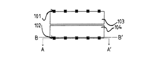
図1は、従来技術で公知の検出素子を示した平面図であり、検出素子の2つの読み出し電極1’、2’および変調ゲート3’、4’が明確に識別可能である。ゲート1’、2’、3’、4’の下側に配置されたシリコン製の感光層については本図中に示されていない。読み出し電極1’、2’は、その作動時に正のバイアス電圧が与えられるため、電極またはゲートは、感光層で生成された電荷キャリアのポテンシャルウエルとして作用する。この正のバイアス電圧は、ホールの移動度が小さいことから、電流移動への寄与が無視可能なように選択される。また、入射電磁放射と変調が一致する変調ゲート3’、4’に対して、参照電圧Urefが印加される。電磁放射の変調と変調ゲート3’、4’の変調電圧は、位相がFΦだけずれた状態とする。強度変調放射の照射時に、感光層において電荷キャリアが生成され、変調ゲート3’、4’によって形成された電位勾配中を、読み出し電極1’、2’まで加速される。変調ゲート3’、4’の下側に位置する感光層の2つの領域間に電位差が生じるように、2つの変調ゲートを逆位相の変調信号でバイアスする必要がある。ここで、読み出し電極1’、2’に到達する電荷キャリア数は、入射電磁放射の強度および位相差FΦの関数である。これにより、入射電磁放射の強度と、入射電磁放射の変調信号と変調ゲート3’、4’の変調信号の位相差FΦは、電圧測定法または電流測定法を用いて記録することができる。 FIG. 1 is a plan view showing a detection element known in the prior art, in which two readout electrodes 1 ′, 2 ′ and modulation gates 3 ′, 4 ′ of the detection element can be clearly identified. The photosensitive layer made of silicon disposed below the gates 1 ′, 2 ′, 3 ′, 4 ′ is not shown in the drawing. Since the read electrodes 1 ′ and 2 ′ are given a positive bias voltage during their operation, the electrode or gate acts as a potential well for charge carriers generated in the photosensitive layer. This positive bias voltage is selected so that the contribution to current transfer is negligible because of the small hole mobility. A reference voltage U ref is applied to the modulation gates 3 ′ and 4 ′ whose modulation matches that of the incident electromagnetic radiation. The modulation of electromagnetic radiation and the modulation voltage of the modulation gates 3 ′ and 4 ′ are in a state where the phase is shifted by FΦ. Upon irradiation with intensity-modulated radiation, charge carriers are generated in the photosensitive layer and accelerated through the potential gradient formed by the modulation gates 3 ′, 4 ′ to the readout electrodes 1 ′, 2 ′. It is necessary to bias the two modulation gates with modulation signals having opposite phases so that a potential difference is generated between the two regions of the photosensitive layer located below the modulation gates 3 ′ and 4 ′. Here, the number of charge carriers reaching the readout electrodes 1 ′, 2 ′ is a function of the intensity of the incident electromagnetic radiation and the phase difference FΦ. Thereby, the intensity of the incident electromagnetic radiation and the phase difference FΦ between the modulation signal of the incident electromagnetic radiation and the modulation signal of the modulation gates 3 ′, 4 ′ can be recorded using a voltage measurement method or a current measurement method.
読み出し電極1’、2’はアルミニウム製のオーミックコンタクトを有しており、半導体材料(代表例としてはp型シリコン)に直接形成されている。この半導体材料は、読み出し電極の金属コンタクト下の領域において、残存材料に対して相補的にn+ドープされており、その結果、pnダイオードが形成される。上記の代わりにn型半導体材料を用いる場合、この半導体材料は、読み出し電極1’、2’のコンタクト下の領域において、pドープされることになる。 The readout electrodes 1 ′ and 2 ′ have an ohmic contact made of aluminum and are directly formed on a semiconductor material (typically p-type silicon). The semiconductor material in the region under the metal contacts of the readout electrodes are complementarily n + doped into the remaining material, as a result, pn diode is formed. When an n-type semiconductor material is used instead of the above, this semiconductor material is p-doped in the region under the contact of the readout electrodes 1 ′ and 2 ′.
図1の平面図においては、読み出し電極の相補的にドープされた領域の底面のみが示されている。その上部における細長片の構造はあまり重要ではない。読み出し電極による読み出しが電圧測定法によって行われる場合、測定電圧信号は1/CA(CAは読み出し電極の容量)に比例する。読み出し電極1’、2’のpn遷移は、読み出し電極の容量CAを本質的に決定する固有容量を有しており、フォトニックミキサー装置内で生成される電荷キャリアに起因する電圧変化を極力大きくするためには、読み出し電極の固有容量は極力小さな値に維持しなければならない。 In the plan view of FIG. 1, only the bottom surface of the complementary doped region of the readout electrode is shown. The structure of the strip at the top is not very important. When reading by the readout electrode is performed by a voltage measurement method, the measurement voltage signal is proportional to 1 / C A (C A is the capacitance of the readout electrode). Readout electrodes 1 ', 2' pn transition has an inherent capacitance which essentially determine the capacitance C A of the read-out electrodes, as much as possible a voltage change caused by charge carriers generated in the photonic mixer device In order to increase the capacitance, the specific capacitance of the readout electrode must be kept as small as possible.
図2は、本発明の好適な第1実施例に係るフォトニックミキサー装置を示した図であり、読み出し電極1、2は、それぞれ分離電極部1A〜1E、2A〜2Eから構成されている。これにより、各読み出し電極1、2の容量は、それぞれ最も離れた2つの分離電極部1A、1Eおよび2A、2E間の距離に原則相当する長さを有する細長片形状の読み出し電極1’、2’よりも小さくなる。読み出し電極1、2の電極部は、上述した変調ゲートから電気的に分離された状態で、空間的に直接隣接した構成である。
FIG. 2 is a view showing a photonic mixer device according to a first preferred embodiment of the present invention, and the readout electrodes 1 and 2 are composed of
図3は、図2中のA−A’線に沿う断面図であり、その断面は、分離電極部を確実に通るものであって、電極部2A〜2Eの縦構造が明確に識別可能である。また、感光層は、シリコン製のp型基板5である。図3の断面図に示すように、各電極部領域において基板がn+ドープ領域6を有しているため、金属コンタクト20A〜20Eを有する電極部2A〜2Eが、ドープ領域の上部に配設され、pnダイオードが形成される。上記の代わりにn型半導体基板を用いる場合、この半導体材料は、電極部領域において、pドープされることになる。また、オーミックコンタクトは、相補的にドープされた領域6に直接形成される。
FIG. 3 is a cross-sectional view taken along the line AA ′ in FIG. 2, and the cross section surely passes through the separation electrode portion, and the vertical structures of the electrode portions 2 </ b> A to 2 </ b> E can be clearly identified. is there. The photosensitive layer is a p-
基板5上の電極間または電極周りには、シリコン酸化層7が配設されている。また、各コンタクト20A〜20Eは、T字形の断面を有する。電極部1A〜1E、2A〜2Eの相補的にドープされた領域6の底面9は、辺長1.8μmの四角形である。図3からも明らかなように、図2、4および以下の図に示される読み出し電極の電極部は、電極部の相補的にドープされた領域6の底面9のみを示している。
A silicon oxide layer 7 is disposed between or around the electrodes on the
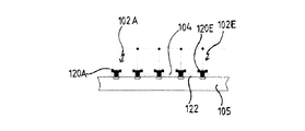
図4に示す分離電極部101A〜101E、102A〜102Eの構成は、各電極部が変調ゲート103、104の領域まで拡張されているという点で、図2に示した構成とは異なる。なお、変調ゲート103、104は、上述した場合と同様に、読み出し電極から電気的に分離されている。この構成により、電極102Cに示すように、原則として3つの側面110、111、112から、電極部への電荷キャリアの着流が改善可能となる。
The configuration of the separation electrode portions 101A to 101E and 102A to 102E shown in FIG. 4 is different from the configuration shown in FIG. 2 in that each electrode portion is extended to the region of the
図5は、図4に示したフォトニックミキサー装置のB−B’線に沿う縦断面図であり、電極部102A〜102Eが変調ゲート104の領域へ突出するとともに、変調ゲートが電極部102A〜102Eおよびそれらのコンタクト120A〜120Eからそれぞれ電気的に分離されているか、または一定の距離隔てられた状態であることが明確に識別可能である。また、この断面図により、変調ゲート104がシリコン酸化層122を介して、その下側のp型シリコン基板から分離されていることが分かる。シリコン酸化層122は、変調ゲート104とシリコン基板105の間の絶縁層として機能する。
FIG. 5 is a longitudinal sectional view taken along the line BB ′ of the photonic mixer device shown in FIG. 4. The electrode portions 102A to 102E protrude into the region of the
図6は、図2および4に示した2つのフォトニックミキサー装置のA−A’線に沿う電位パターンを示した図であり、読み出し電極1、2、101、102が、その正のバイアス電圧によって、光子から生成される電子をトラップ可能なポテンシャルウエルを形成していることが明らかである。
FIG. 6 is a diagram showing a potential pattern along the line AA ′ of the two photonic mixer devices shown in FIGS. 2 and 4, and the
図7は、3つの混合素子213、214、215を備えたフォトニックミキサー装置を示している。混合素子213〜215は、それぞれ2つの読み出し電極201、202、216、217を有する。これらの各読み出し電極は、図2および4と同様に、それぞれ5つの分離電極部から構成されている。
FIG. 7 shows a photonic mixer device comprising three mixing
混合素子213、215は、その間に配置された混合素子214と共通で、それぞれ読み出し電極216、217を使用する。混合素子213〜215によって共通に使用される読み出し電極216、217は、表面積が大きな2つの変調ゲート218、219の領域に配置されている。この2つの変調ゲート218、219は、原則として、図2および4に示したフォトニックミキサー装置の変調ゲートの2倍幅広となっている。変調ゲート218、219は、読み出し電極216、217と同様に、2つの隣接するフォトニックミキサー装置によって共通に使用される。また、変調ゲート218〜221は、各隣接する変調ゲートが変調信号によって逆位相で動作するように接続される。それぞれの場合において、4つの読み出し電極201、202、216、217のうちの2つを相互接続し、共通に読み出しを行う。同相の変調信号が供給される変調ゲートに隣接する2つのゲートは、常に接続された状態となる。
The mixing
検出素子213、215に含まれる外側の2つの読み出し電極201、202は、それぞれ図4に示す読み出し電極101、102と同様に構成されているが、図7に示す読み出し電極201、202は、その全体が変調ゲート220、221の領域に存在するため、図4の読み出し電極101、102のようにちょうど半分がゲート領域中に存在する場合とは異なる。
The outer two
上記とは別の実施例として、図7の構成とは異なり、4つ以上の混合素子を接続してフォトニックミキサー装置を構成することも可能である。また、図7に示す3つ構成の混合素子を、フォトニックミキサー装置上に2つ並べて配置することも可能である。この場合、3つ構成の混合素子それぞれの変調信号は、互いに位相が90°ずれた状態となり、その結果、入射電磁放射の直交成分と同時に、強度と位相についても1回の測定で記録することが可能となる。 As an embodiment different from the above, unlike the configuration of FIG. 7, it is also possible to configure a photonic mixer device by connecting four or more mixing elements. It is also possible to arrange two mixing elements shown in FIG. 7 side by side on the photonic mixer device. In this case, the modulation signals of the three mixed elements are in a state where the phases are shifted from each other by 90 °. As a result, the intensity and phase are recorded in one measurement simultaneously with the orthogonal component of the incident electromagnetic radiation. Is possible.
図8Aにその他の実施例に係るフォトニックミキサー装置を示す。読み出し電極301、302は、変調ゲート303、304に隣接する新たなメモリーゲート323、324によって囲われている。メモリーゲート323、324には正の直流電圧がバイアスされているため、図8AのA−A’線に沿う電位分布は図8Bのようになる。なお、印加バイアス電圧は、メモリーゲート下のシリコン基板中にメモリーゲートによって形成されるポテンシャルウエルの電位が、読み出し電極302の電極よりも高くなるように選択される。このメモリーゲートによって、光子から生成される電子に対する大きなポテンシャルウエルが形成される。読み出し電極301、302の内部または周囲に電位勾配が形成されると、照射強度が低い場合、分割ダイオードの固有容量が小さいために、電荷キャリアによって大きな電圧レベル変化がもたらされる。他方、照射強度が高く、フォトニックミキサー装置内で多数の電子が生成されている場合は、これら電子によって読み出し電極のポテンシャル井戸がすぐに満たされてしまい、さらなる電子はメモリーゲート323、324に捕集されることになる。この際、メモリーゲートの容量が大きいことから、電荷キャリア当たりの電圧レベル変化は小さなものとなる。要約すれば、照射強度が低い場合は高感度が得られる一方、照射強度がメモリーゲートのバイアス電圧によって決まる特定の閾値をいったん超えると、感度は低い値となる。このようにして、本発明のフォトニックミキサー装置のダイナミックレンジは、メモリーゲートを持たないフォトニックミキサー装置よりも大幅に拡張される。
FIG. 8A shows a photonic mixer device according to another embodiment. The read
図9Aは、上記をさらに拡張した実施例に係るメモリーゲート423、424を備えたフォトニックミキサー装置を示しており、追加メモリーゲート425、426を備えた2つの新たなメモリー構造が、シリコン基板上で実混合素子の横に配置されている。追加メモリーゲート425、426は、互いに電気的に分離されているとともに、フォトニックミキサー装置の残存ゲートからも電気的に分離されている。追加メモリーゲート425、426の領域には、分離点電極から構成された読み出し電極427、428も配置されており、これらの読み出し電極427、428は、それぞれ読み出し電極401、402と電気的に接続されている。読み出し電極427、428を備えた追加メモリーゲート425、426は、金属層で覆われているため、その部分には電磁放射が一切印加されない(図9Aに図示せず)。また、追加メモリーゲート425、426は、上記と同様に直流電圧がバイアスされており、追加メモリーゲート425、426のバイアス電圧の絶対値は、メモリーゲート423、424のバイアス電圧の絶対値よりも大きい。
FIG. 9A shows a photonic mixer device with
追加メモリーゲート425、426の作用は、図9A中のB−B’線およびA−A’線に沿う電位パターンを示した図9Bから明らかとなる。この図において再度、読み出し電極の電極によって形成されるポテンシャルウエル429が明確に識別可能となっている。追加メモリーゲート425、426を備えたメモリー構造の新たな容量により、放射強度に応じて、フォトニックミキサー装置の電荷変換効率がさらに3段階形成される。強度に依存する電荷変換効率または感度により、本実施例の検出器のダイナミックレンジが拡張されることは明らかである。
The operation of the
図10および11は、3つの検出素子513〜515および613〜615をそれぞれフォトニックミキサー装置上に集積した場合の2実施例であり、読み出し電極501、502、516、517、および601、602、616、617は、それぞれメモリーゲートによって囲われている。この2実施例の相違点は以下の通りである。図10の実施例の場合は、メモリーゲートが、読み出し電極とそれぞれ対応する変調ゲートとの間で、2つの狭隘な細長片531、532の形で設けられている一方、図11の実施例の場合は、読み出し電極が幅広のメモリーゲート633内に配置されている。
FIGS. 10 and 11 are two examples when three
図8A、9A、10および11に示すメモリーゲート323、324、423、424、531、532、633は、そのバイアス電圧が一定であるため、変調ゲート303、304、403、404、および、読み出し電極301、302、401、402、501、502、516、517の間の電気的クロストークを低減する効果がある。このようにして、読み出し電極は、変調ゲート303、304、403、404における高周波変調の悪影響から完全に切り離すことができる。
The
Claims (37)
前記他の読み出し電極(427、428)は、電気的に相互接続されている他の分離電極部を有し、
前記他の読み出し電極(427、428)の分離電極部は、前記他のメモリーゲート(425、426)から電気的に分離され、
前記メモリー構造は、電磁放射に対して不透明な層で覆われ、
前記他の読み出し電極(427、428)は、前記読み出し電極(401、402)と電気的に接続されたことを特徴とする、請求項31に記載のフォトニックミキサー装置。 The memory structure has at least one other read electrode (427, 428) with another memory gate (425, 426) and is configured such that the other memory gate surrounds the other read electrode. ,
The other readout electrodes (427, 428) have other separation electrode portions that are electrically interconnected,
The separation electrode portion of the other readout electrode (427, 428) is electrically separated from the other memory gate (425, 426),
The memory structure is covered with a layer opaque to electromagnetic radiation;
32. The photonic mixer device according to claim 31, wherein the other readout electrodes (427, 428) are electrically connected to the readout electrodes (401, 402).
Applications Claiming Priority (2)
| Application Number | Priority Date | Filing Date | Title |
|---|---|---|---|
| DE102004016624.2 | 2004-04-05 | ||
| DE102004016624A DE102004016624A1 (en) | 2004-04-05 | 2004-04-05 | Photonic Mixer Device |
Publications (3)
| Publication Number | Publication Date |
|---|---|
| JP2006023276A JP2006023276A (en) | 2006-01-26 |
| JP2006023276A5 JP2006023276A5 (en) | 2011-02-24 |
| JP4786924B2 true JP4786924B2 (en) | 2011-10-05 |
Family
ID=34895472
Family Applications (1)
| Application Number | Title | Priority Date | Filing Date |
|---|---|---|---|
| JP2005107084A Active JP4786924B2 (en) | 2004-04-05 | 2005-04-04 | Photonic mixer device |
Country Status (6)
| Country | Link |
|---|---|
| US (1) | US7361883B2 (en) |
| EP (1) | EP1584904B1 (en) |
| JP (1) | JP4786924B2 (en) |
| CN (1) | CN1680792A (en) |
| AT (1) | ATE396388T1 (en) |
| DE (2) | DE102004016624A1 (en) |
Families Citing this family (11)
| Publication number | Priority date | Publication date | Assignee | Title |
|---|---|---|---|---|
| US7420148B2 (en) * | 2002-09-13 | 2008-09-02 | Conti Temic Microelectronic Gmbh | Method and device for determining a pixel gray scale value image |
| DE102004044581B4 (en) * | 2004-09-13 | 2014-12-18 | Pmdtechnologies Gmbh | Method and device for runtime-sensitive measurement of a signal |
| KR101623960B1 (en) | 2009-06-04 | 2016-05-25 | 삼성전자주식회사 | Optoelectronic shutter, method of operating the same and optical apparatus employing the optoelectronic shutter |
| DE102012109548B4 (en) | 2012-10-08 | 2024-06-27 | pmdtechnologies ag | Readout gate |
| DE102013102061A1 (en) | 2013-03-01 | 2014-09-04 | Pmd Technologies Gmbh | Semiconductor component for detecting electromagnetic radiation of photosensitive semiconductor substrate, has first and second substrate portions having read-out nodes whose charge carriers are read out and do not pass from one to other |
| DE102013109020B4 (en) | 2013-08-21 | 2016-06-09 | Pmdtechnologies Gmbh | Scattered light reference pixel |
| DE102015108961A1 (en) | 2015-06-08 | 2016-12-08 | Pmdtechnologies Gmbh | image sensor |
| US10191154B2 (en) | 2016-02-11 | 2019-01-29 | Massachusetts Institute Of Technology | Methods and apparatus for time-of-flight imaging |
| US10190983B2 (en) | 2016-04-15 | 2019-01-29 | Massachusetts Institute Of Technology | Methods and apparatus for fluorescence lifetime imaging with pulsed light |
| CN109004060B (en) * | 2017-06-26 | 2019-11-05 | 苏州科技大学 | Terahertz wave detector |
| US10310085B2 (en) | 2017-07-07 | 2019-06-04 | Mezmeriz Inc. | Photonic integrated distance measuring pixel and method of distance measurement |
Family Cites Families (8)
| Publication number | Priority date | Publication date | Assignee | Title |
|---|---|---|---|---|
| CZ300055B6 (en) * | 1996-09-05 | 2009-01-21 | Method of determining the phase and/or amplitude information of an electromagnetic wave, photonic mixing element, mixing element arrangement and apparatus for making the same | |
| DE19704496C2 (en) * | 1996-09-05 | 2001-02-15 | Rudolf Schwarte | Method and device for determining the phase and / or amplitude information of an electromagnetic wave |
| DE19821974B4 (en) * | 1998-05-18 | 2008-04-10 | Schwarte, Rudolf, Prof. Dr.-Ing. | Apparatus and method for detecting phase and amplitude of electromagnetic waves |
| US7211818B2 (en) * | 1999-03-24 | 2007-05-01 | Fujifilm Corporation | Image read-out method and system, solid image sensor, and image detecting sheet |
| ITMI20010443A1 (en) * | 2001-03-02 | 2002-09-02 | Marconi Comm Spa | METHOD AND APPARATUS FOR THE DETECTION AND COMPENSATION OF PMD PARAMETERS IN SIGNALS LONG TRANSMITTED CONNECTIONS TO FIBER OPTICS AND SYSTEMS |
| GB2389960A (en) * | 2002-06-20 | 2003-12-24 | Suisse Electronique Microtech | Four-tap demodulation pixel |
| DE10230225B4 (en) * | 2002-07-04 | 2006-05-11 | Zentrum Mikroelektronik Dresden Ag | Photonic mixer and method of its operation and manufacture |
| WO2004027359A1 (en) * | 2002-09-13 | 2004-04-01 | Conti Temic Microelectronic Gmbh | Method and device for determining a pixel gray scale value image |
-
2004
- 2004-04-05 DE DE102004016624A patent/DE102004016624A1/en not_active Withdrawn
-
2005
- 2005-03-18 EP EP05102192A patent/EP1584904B1/en active Active
- 2005-03-18 AT AT05102192T patent/ATE396388T1/en not_active IP Right Cessation
- 2005-03-18 DE DE502005004162T patent/DE502005004162D1/en active Active
- 2005-04-04 JP JP2005107084A patent/JP4786924B2/en active Active
- 2005-04-04 US US11/098,728 patent/US7361883B2/en active Active
- 2005-04-05 CN CNA2005100648903A patent/CN1680792A/en active Pending
Also Published As
| Publication number | Publication date |
|---|---|
| EP1584904A3 (en) | 2007-05-30 |
| US20050237811A1 (en) | 2005-10-27 |
| US7361883B2 (en) | 2008-04-22 |
| DE502005004162D1 (en) | 2008-07-03 |
| DE102004016624A1 (en) | 2005-10-13 |
| EP1584904A2 (en) | 2005-10-12 |
| ATE396388T1 (en) | 2008-06-15 |
| CN1680792A (en) | 2005-10-12 |
| JP2006023276A (en) | 2006-01-26 |
| EP1584904B1 (en) | 2008-05-21 |
Similar Documents
| Publication | Publication Date | Title |
|---|---|---|
| JP4786924B2 (en) | Photonic mixer device | |
| US10795003B2 (en) | High-speed light sensing apparatus | |
| TW202209697A (en) | Circuit for digitizing measurement | |
| US11709238B2 (en) | Demodulator with a carrier generating pinned photodiode and a method for operating it | |
| KR20110040720A (en) | Photonic mixer and use thereof | |
| US20090026508A1 (en) | Solid-state photosensor with electronic aperture control | |
| US7622704B2 (en) | Optoelectronic detector with multiple readout nodes and its use thereof | |
| US4427990A (en) | Semiconductor photo-electric converter with insulated gate over p-n charge storage region | |
| KR20140146088A (en) | Pn-structured gate demodulation pixel | |
| TW202038462A (en) | Semiconductor device with low dark noise | |
| JPS5928110B2 (en) | Infrared image sensor circuit layout | |
| US8884394B2 (en) | Range sensor and range image sensor | |
| JP2009238940A (en) | Photodiode and imaging element including the same | |
| US11532663B2 (en) | Demodulator with a carrier generating pinned photodiode | |
| JPS5928072B2 (en) | radiation sensing device | |
| US7619240B2 (en) | Semiconductor photodetector, device for multispectrum detection of electromagnetic radiation using such a photodetector and method for using such a device | |
| US5019876A (en) | Semiconductor photo-electric converter | |
| RU2185689C2 (en) | Avalanche photodetector (versions) | |
| US20060284275A1 (en) | Optical sensor element and sensor array | |
| Metzler et al. | Ultrathin, two-dimensional, multi-element Si pin photodiode array for multipurpose applications | |
| US20240038908A1 (en) | Photo sensor cell, photo sensor and method | |
| CN110277462B (en) | Electrically modulated photodiode and method of manufacturing the same | |
| Langfelder | Design of a fully CMOS compatible 3-μm size color pixel | |
| Haralson et al. | Theoretical study of a GaAs lateral pin photodetector | |
| Hoskins et al. | High speed GaAs acoustic charge transport multiplexer |
Legal Events
| Date | Code | Title | Description |
|---|---|---|---|
| A621 | Written request for application examination |
Free format text: JAPANESE INTERMEDIATE CODE: A621 Effective date: 20080303 |
|
| A131 | Notification of reasons for refusal |
Free format text: JAPANESE INTERMEDIATE CODE: A131 Effective date: 20100629 |
|
| A601 | Written request for extension of time |
Free format text: JAPANESE INTERMEDIATE CODE: A601 Effective date: 20100909 |
|
| A602 | Written permission of extension of time |
Free format text: JAPANESE INTERMEDIATE CODE: A602 Effective date: 20100914 |
|
| A521 | Request for written amendment filed |
Free format text: JAPANESE INTERMEDIATE CODE: A523 Effective date: 20101216 |
|
| A524 | Written submission of copy of amendment under article 19 pct |
Free format text: JAPANESE INTERMEDIATE CODE: A524 Effective date: 20101216 |
|
| A131 | Notification of reasons for refusal |
Free format text: JAPANESE INTERMEDIATE CODE: A131 Effective date: 20110315 |
|
| A521 | Request for written amendment filed |
Free format text: JAPANESE INTERMEDIATE CODE: A523 Effective date: 20110526 |
|
| TRDD | Decision of grant or rejection written | ||
| A01 | Written decision to grant a patent or to grant a registration (utility model) |
Free format text: JAPANESE INTERMEDIATE CODE: A01 Effective date: 20110621 |
|
| A01 | Written decision to grant a patent or to grant a registration (utility model) |
Free format text: JAPANESE INTERMEDIATE CODE: A01 |
|
| A61 | First payment of annual fees (during grant procedure) |
Free format text: JAPANESE INTERMEDIATE CODE: A61 Effective date: 20110714 |
|
| R150 | Certificate of patent or registration of utility model |
Ref document number: 4786924 Country of ref document: JP Free format text: JAPANESE INTERMEDIATE CODE: R150 Free format text: JAPANESE INTERMEDIATE CODE: R150 |
|
| FPAY | Renewal fee payment (event date is renewal date of database) |
Free format text: PAYMENT UNTIL: 20140722 Year of fee payment: 3 |
|
| R250 | Receipt of annual fees |
Free format text: JAPANESE INTERMEDIATE CODE: R250 |
|
| R250 | Receipt of annual fees |
Free format text: JAPANESE INTERMEDIATE CODE: R250 |
|
| R250 | Receipt of annual fees |
Free format text: JAPANESE INTERMEDIATE CODE: R250 |
|
| R250 | Receipt of annual fees |
Free format text: JAPANESE INTERMEDIATE CODE: R250 |
|
| R250 | Receipt of annual fees |
Free format text: JAPANESE INTERMEDIATE CODE: R250 |
|
| R250 | Receipt of annual fees |
Free format text: JAPANESE INTERMEDIATE CODE: R250 |
|
| R250 | Receipt of annual fees |
Free format text: JAPANESE INTERMEDIATE CODE: R250 |
|
| R250 | Receipt of annual fees |
Free format text: JAPANESE INTERMEDIATE CODE: R250 |
|
| R250 | Receipt of annual fees |
Free format text: JAPANESE INTERMEDIATE CODE: R250 |
|
| R250 | Receipt of annual fees |
Free format text: JAPANESE INTERMEDIATE CODE: R250 |
|
| R250 | Receipt of annual fees |
Free format text: JAPANESE INTERMEDIATE CODE: R250 |