JP4782019B2 - Apparatus and method for optical measurement of optical system, measurement structure support, and microlithography projection exposure apparatus - Google Patents
Apparatus and method for optical measurement of optical system, measurement structure support, and microlithography projection exposure apparatus Download PDFInfo
- Publication number
- JP4782019B2 JP4782019B2 JP2006548246A JP2006548246A JP4782019B2 JP 4782019 B2 JP4782019 B2 JP 4782019B2 JP 2006548246 A JP2006548246 A JP 2006548246A JP 2006548246 A JP2006548246 A JP 2006548246A JP 4782019 B2 JP4782019 B2 JP 4782019B2
- Authority
- JP
- Japan
- Prior art keywords
- measurement
- radiation
- detector
- measurement structure
- source
- Prior art date
- Legal status (The legal status is an assumption and is not a legal conclusion. Google has not performed a legal analysis and makes no representation as to the accuracy of the status listed.)
- Expired - Fee Related
Links
Images


Classifications
-
- G—PHYSICS
- G03—PHOTOGRAPHY; CINEMATOGRAPHY; ANALOGOUS TECHNIQUES USING WAVES OTHER THAN OPTICAL WAVES; ELECTROGRAPHY; HOLOGRAPHY
- G03F—PHOTOMECHANICAL PRODUCTION OF TEXTURED OR PATTERNED SURFACES, e.g. FOR PRINTING, FOR PROCESSING OF SEMICONDUCTOR DEVICES; MATERIALS THEREFOR; ORIGINALS THEREFOR; APPARATUS SPECIALLY ADAPTED THEREFOR
- G03F7/00—Photomechanical, e.g. photolithographic, production of textured or patterned surfaces, e.g. printing surfaces; Materials therefor, e.g. comprising photoresists; Apparatus specially adapted therefor
- G03F7/70—Microphotolithographic exposure; Apparatus therefor
- G03F7/70483—Information management; Active and passive control; Testing; Wafer monitoring, e.g. pattern monitoring
Description
本発明は、有効な操作モードにおいて有効な放射線入射側で有効な放射線を受け取り、有効な放射線出射側でそれを放射する光学系の光学測定のための装置であって、測定放射線を光学系に放射する少なくとも1つの出射側要素(exit-side element)を、それによって光学系の有効な放射線出射側に配置することができる測定放射線ソース(measurement radiation source)と、光学系から出現する測定放射線を受け取る少なくとも1つの入射側要素(entrance-side element)を、このような装置のために使用できる測定構造支持材(measurement structure support)に対する光学系の有効な放射線入射側に配置することができる検出器とを備える装置に関し、このような装置を備えるマイクロリソグラフィ投影露光装置に関し、及び、関連する方法に関する。 The present invention is an apparatus for optical measurement of an optical system that receives an effective radiation at an effective radiation incident side and emits it at an effective radiation exit side in an effective operation mode, wherein the measurement radiation is transmitted to the optical system. A measurement radiation source capable of placing at least one exit-side element to radiate on the effective radiation exit side of the optical system, and a measurement radiation emerging from the optical system Detector capable of placing at least one entrance-side element to be received on the effective radiation entrance side of the optical system relative to a measurement structure support that can be used for such a device A microlithographic projection exposure apparatus comprising such an apparatus, and an associated method.
光学結像系のような光学系の測定用装置は、様々に知られている。光学系の有効動作モード(useful operating mode)では、有効な放射線が有効な放射線方向で、例えば有効な入射側、つまり物体側で照明されている物体から、光学系まで通過し、後者を通り抜け、有効な出射側、つまり像側の光学系から出現する。 Various measuring devices for an optical system such as an optical imaging system are known. In the useful operating mode of the optical system, effective radiation passes in the effective radiation direction, for example from an object that is illuminated on the effective incident side, ie the object side, to the optical system, through the latter, It emerges from the optical system on the effective exit side, that is, the image side.
光学系の測定の場合、例えばマイクロリソグラフィのための投影対物レンズ(projection objective)等の結像系の場合での結像異常に関して、それは測定動作モードで操作される。この動作モードでは、通常、測定放射線を放射するための測定放射線ソースが物体側に配置され、測定放射線を受け取るための検出器は像側に配置される。この場合では、単一の測定放射線発生装置が、一方では測定動作モードで測定放射線ソースのために、他方では有効動作モードで有効な放射線源のために設けられてよい。 In the case of measurement of optical systems, for example, imaging abnormalities in the case of imaging systems such as projection objectives for microlithography, it is operated in a measurement mode of operation. In this mode of operation, typically a measurement radiation source for emitting measurement radiation is arranged on the object side and a detector for receiving measurement radiation is arranged on the image side. In this case, a single measurement radiation generator may be provided on the one hand for the measurement radiation source in the measurement operation mode and on the other hand for the radiation source effective in the effective operation mode.
独国特許出願公開第101 09 929号明細書は光学系の波面測定のための装置を説明しており、光学系の後ろに回折格子と、回折格子の下流に配置される空間的に分解する検出器素子とを備える検出器が像側に設けられているが、その装置は測定放射線ソースとして物体側に配置されなければならず、光学系を通過する波面を生成するための二次元ソース側測定構造マスクを有する波面ソースを備える。波面測定には、回折格子が側面方向に変位されるシヤリング干渉計測技法が使用される。点回折干渉技法(point diffraction interfererometry)、モアレ方法、及びシャック−ハートマン(Shack−Hartmann)方法等の他の測定技法を使用する波面測定装置が代替策として通例である。この場合では、測定に使用される放射線は、光学系の通常の動作中に使用される有効放射線と同一であってよい。 DE 101 09 929 describes a device for measuring the wavefront of an optical system, with a diffraction grating behind the optical system and a spatially resolved arrangement arranged downstream of the diffraction grating. A detector comprising a detector element is provided on the image side, but the device must be arranged on the object side as a measurement radiation source and is a two-dimensional source side for generating a wavefront passing through the optical system A wavefront source having a measurement structure mask is provided. The wavefront measurement uses a shearing interferometry technique in which the diffraction grating is displaced in the lateral direction. Wavefront measurement devices that use other measurement techniques such as point diffraction interfererometry, moire methods, and Shack-Hartmann methods are typically an alternative. In this case, the radiation used for the measurement may be the same as the effective radiation used during normal operation of the optical system.
1つの重要な応用分野は、それらの役に立つサイトでの、対応するステッパ又はスキャナ等のリソグラフィ露光装置における投影対物レンズの測定である。この目的のために、測定放射源を少なくとも部分的に、特に関連する測定構造マスクをレチクルに統合すること、あるいは従来のレチクル段階とレチクルを交換するためにそれを装置に導入すること、及び/又は少なくとも部分的に検出器をウェハステージに統合すること、あるいはウェハをウェハステージと交換するためにそれを装置に導入することはすでに提案されていた。検出器がウェハステージに統合されると、相対的に少ししか構造上の空間が利用できず、特にその電子構成部品内で検出器が発する熱が上にある投影対物レンズに影響を及ぼす可能性があるという問題がある。 One important application area is the measurement of projection objectives in lithographic exposure apparatus such as corresponding steppers or scanners at their useful sites. For this purpose, the measurement radiation source is at least partly integrated, in particular the relevant measurement structure mask, into the reticle, or it is introduced into the apparatus to replace the reticle with a conventional reticle stage, and / or Or it has already been proposed to at least partially integrate the detector into the wafer stage or to introduce it into the apparatus to replace the wafer with the wafer stage. When the detector is integrated into the wafer stage, relatively little structural space is available, especially the heat generated by the detector in its electronic components can affect the projection objective on top. There is a problem that there is.
米国特許第5,978,085号明細書に説明されているようなシャック−ハートマン測定方法の場合では、その構造がフォトレジストでコーティングされた検出器ウェハ上に露呈される複雑な測定レチクルが使用される。評価は、適切な測定装置によって露光装置の外部の検出器ウェハ上に作られた測定構造によって達成される。この手順は比較的に時間を要する。 In the case of the Shack-Hartman measurement method as described in US Pat. No. 5,978,085, a complex measurement reticle is used whose structure is exposed on a photoresist-coated detector wafer. Is done. The evaluation is achieved by a measurement structure made on a detector wafer external to the exposure apparatus by a suitable measurement device. This procedure is relatively time consuming.
本米国特許第6,278,514号明細書は、二重通過方法に基づいて動作する波面収差を決定するための装置がその中に統合される投影露光装置を説明している。この目的のため、それは鏡等の、ウェハ保持領域に沿ったウェハステージの中に統合され、投影対物レンズから出現する光を後者に反射し直し、その結果それが同じ光路上であるが、反対方向で二度目に投影対物レンズを通過するビーム偏向装置を備える。その後、光はレチクル平面と投影対物レンズの間に配置されるハーフミラー(semitransparent mirror)によって検出器素子の方向で側面方向に外部結合(coupled out)される。 US Pat. No. 6,278,514 describes a projection exposure apparatus in which an apparatus for determining wavefront aberrations operating based on a double-pass method is integrated. For this purpose, it is integrated into a wafer stage along the wafer holding area, such as a mirror, to reflect the light emerging from the projection objective back to the latter so that it is on the same optical path but the opposite A beam deflection device is provided that passes through the projection objective a second time in the direction. The light is then coupled out laterally in the direction of the detector element by a semitransparent mirror arranged between the reticle plane and the projection objective.
公開された国際公開第2004/057295号パンフレット及び出願人による対応する米国出願は、例えば、浸漬液チャンバとして構成されているビーム経路内の連続する光学部品間の対応する隙間によって測定装置の1つ又は複数の物体側の、及び/又は1つ又は複数の像側の部品の内の少なくとも1つの近傍に導入できる浸漬液と動作する、マイクロリソグラフィ投影対物レンズ等の光学系の光学測定のための装置及び方法を説明している。これらの2つの文書の内容は、不必要なテキストの繰り返しを回避するためにこの浸漬液主題に関して本明細書に完全に参照することにより組み込まれている。 Published International Publication No. WO 2004/057295 and the corresponding US application by the applicant are one of the measuring devices, for example by means of a corresponding gap between successive optical components in the beam path configured as an immersion liquid chamber. Or for optical measurements of optical systems, such as microlithographic projection objectives, working with immersion liquids that can be introduced in the vicinity of at least one of the object-side and / or one or more image-side components An apparatus and method are described. The contents of these two documents are incorporated by full reference herein to this immersion liquid subject to avoid unnecessary text repetition.
本発明が基づいている技術的な問題は光学系の測定のための手引きに言及された型の装置を提供する問題であり、その装置は、特にリソグラフィ露光装置の投影対物レンズの測定中の機能上の、及び技術的な取り扱い優位点を提供し、この目的のためのこのような露光装置においてレトロフィットさせることもできる。さらに、これに適した測定構造支持材、及びこのような装置を備えたマイクロリソグラフィ投影露光装置を提供することを目的とする。 The technical problem on which the present invention is based is that of providing an apparatus of the type mentioned in the guidance for the measurement of optical systems, which function in particular during the measurement of the projection objective of a lithographic exposure apparatus. It provides the above and technical handling advantages and can also be retrofitted in such an exposure apparatus for this purpose. It is another object of the present invention to provide a measurement structure support material suitable for this, and a microlithographic projection exposure apparatus including such an apparatus.
本発明は、請求項1の特徴を備える装置、請求項12の特徴を備える測定構造支持材、請求項21の特徴を備えるマイクロリソグラフィ投影露光装置、及び請求項24の特徴を備える方法を提供することによりこの問題を解決する。
The invention provides an apparatus comprising the features of
請求項1に記載の本発明による装置の場合では、測定放射線ソースは、有効放射出射側で位置決めするためのソース側測定構造マスクを備え、及び/又は検出器は有効放射入射側で位置決めするための検出器側測定構造マスクを備える。したがって、測定動作中、測定放射線は、有効放射線が有効な動作で光学系を通過する方向に反対の方向で光学系を通過する。有効動作を基準にして反対方向の測定放射線のこのビーム誘導によって、特にリソグラフィ露光装置の投影対物レンズの測定中に、測定動作の測定放射線が有効動作の有効放射線と同じ方向で投影対物レンズを通過する従来の装置の前述の問題を完全に又は部分的に回避することが可能である。したがって、おそらく閉じ込められた像側領域内に検出器構成部品を装置する必要はなく、ウェハステッパシステム及びウェハスキャナシステム等の既存の装置は、主として型に関係なくこの装置とすでにレトロフィットできる。この目的のため、測定放射源の構成部品は完全に又は部分的に像側に配置できる特にソース側測定構造マスクは、例えばウェハステージを介して導入できる。検出器の構成部品は完全に又は部分的に物体側に配置できる。特に、検出器側測定構造マスクは、例えば対物レンズのレチクル平面内等の物体側に配置できる。
In the case of the device according to the invention as claimed in
請求項2に記載の本発明の開発の場合では、測定放射線ソースはソース側測定構造マスクの背面照明用に設計され、ソース側測定構造マスクは伝播中の動作のために設計され、測定放射線ソースは、ソース側測定構造マスクの上流の測定放射線のビーム経路内に測定放射線変換装置を備える。測定放射線変換装置は、測定放射線がソース側測定構造マスクを輝度と方向に関して主として均一的に、非干渉に、及び完全に照明するように便宜上形成される。測定ビーム方向の均一な分布は、統一した、あるいは少なくとも単にゆっくりと変化する瞳孔の照明を引き起こし、ソース側測定構造マスクでの輝度の均一な分布は検出器側の測定構造マスクでの均一な輝度の分布を引き起こす。
In the case of the development of the invention as claimed in
請求項3に記載の装置の場合では、測定放射線変換装置は、1つ又は複数の光偏向素子及び/又は1つ又は複数の光散乱素子を有する。例証として、粗い表面、マイクロプリズム又は回折格子が光散乱素子として働いてよい。反射素子は、例えば光導波管、プリズム又は鏡として実現されてよく、低損失複数反射によって、光量と混合の両方に関してビーム変換の習熟を高める。このような反射構造及び光散乱構造は製造するのが単純で、費用効果が高い。
In the case of the device according to
請求項4に記載の装置の開発においては、測定放射線ソースは、有効放射入射側で位置決めするためのビーム発生装置を備え、検出器側測定構造マスクは、測定構造領域の外で、測定放射線のための通過領域を有する。測定放射線は通過領域を通って検出器を横断し、ビーム発生装置からソース側測定構造マスクに通過できる。使用されるビーム発生装置は、この場合では特に、光学系の有効動作中に有効な放射線を供給するものであってよい。
In the development of the apparatus according to
請求項5に記載の装置の場合では、ソース側測定構造マスクは、測定構造領域の背面照明のためのビーム発生装置によって発せられる測定放射線を通過するために、測定構造領域の外部に通過領域を有する。これは、測定構造領域に通過する測定放射線を偏向するビーム偏向素子によって支えられてよい。
In the case of the apparatus according to
請求項6に記載の装置の場合では、測定放射線ソースは、ソース側測定構造マスクの前面照明のために設計され、ソース側測定構造マスクは反射中の動作のために設計される。これは、特に、EUV範囲の、つまり100nm未満の波長を有する測定放射線が使用されるときに有効である可能性がある。請求項7に記載の追加の改善では、ソース側測定構造マスクの測定構造領域は一方で散乱領域を、他方では反射及び/又は吸収領域を有する。反射中動作する測定構造マスクの散乱領域は伝播中動作する測定構造マスクの透明な領域に相当し、開口角の外部で反射する、及び/又は吸収する領域はマスクの不透明な領域に相当する。
In the case of the apparatus according to
請求項8に記載の装置は、ビーム発生装置によってソース側測定構造マスクの前又は後ろの領域の中に発せられる測定放射線を側面方向で供給するための測定放射線誘導装置を有する。使用される測定放射線誘導装置は、例えば、集光効果と散乱効果の両方を有するように形成される鏡セグメントであってよい。全反射を利用する狭い入射角は、EUV範囲内の短波放射線の場合で有利である。側面方向の供給には屈折集光光学部品又は光導波管も使用されてよい。側面方向に供給される測定放射線を提供するには製造するのが簡単で費用効果の高いビーム発生装置で十分である。 The device according to claim 8 comprises a measuring radiation guiding device for supplying in a lateral direction measuring radiation emitted by the beam generator into the area in front of or behind the source-side measuring structure mask. The measuring radiation guidance device used may be, for example, a mirror segment that is formed to have both light collection and scattering effects. A narrow angle of incidence that utilizes total internal reflection is advantageous in the case of shortwave radiation in the EUV range. Refractive focusing optics or optical waveguides may also be used for lateral delivery. A beam generator that is simple to manufacture and cost-effective is sufficient to provide the measurement radiation delivered in the lateral direction.
請求項9による装置の開発では、検出器は、光学系の有効放射入射側に配置される検出器支持材を有し、検出器支持材は検出器側測定構造マスクと下流に配置される検出器素子を支えている。検出器支持材は、それが、例えばシヤリング干渉計側技法によって波面測定を実行するために必要に応じて側面方向で変位できるように配置されてよい。検出器素子は例えばCCD装置、CMOS装置、又はCID装置等の高速見当合せに適したオプトエレクトロニック装置、あるいは光の輝度を光科学的に、及び空間に依存した様式で測定する装置であってよい。必要とされる電子部品は非常に平坦な設計で実現されてよい。 In the development of the device according to claim 9, the detector has a detector support arranged on the effective radiation incident side of the optical system, the detector support being located downstream from the detector-side measuring structure mask. Supports the vessel element. The detector support may be arranged so that it can be displaced laterally as needed to perform wavefront measurements, for example by shearing interferometer side techniques. The detector element may be an optoelectronic device suitable for high-speed registration, such as a CCD device, a CMOS device, or a CID device, or a device that measures the brightness of light in an optically and spatially dependent manner. . The required electronic components may be realized with a very flat design.
請求項10に記載の装置の開発では、検出器支持材が検出器電源を支えている。その結果、検出器は、光学系の有効放射入射側に配置できる自律可搬式装置として具現化されてよい。検出器支持材は任意で結像光学系、カメラ、電子制御装置、画像メモリ及び/又はワイヤフリーの通信装置を有してもよい。
In the development of the device according to
請求項11による装置の開発では、浸漬液は測定放射線ソースの中に、又は測定放射線ソースの近傍に及び/又は検出器の中に又は検出器の近傍に導入でき、その結果これに関連する有利点を活用できる。
In the development of the device according to
請求項12に記載の本発明による測定構造支持材は透明な支持材本体を有し、その前面には伝播中に動作可能であり、測定構造領域を備え、その中に測定構造領域の背面照明のための測定放射線変換装置が統合される測定構造マスクが設けられ、測定構造支持材は前面に、測定構造マスクの測定構造領域の外部の前面に、及び/又は背面に測定放射線を支持材本体に結合する(coupled in)ための通過領域を有する。測定構造支持材は、例えば、透明な材料を備え、一面で測定構造マスクを支えるプレートとして具現化されてよい。測定構造マスク付きの測定構造支持材は、例えばシヤリング干渉計側技法によって波面測定を実行することが意図される場合に、必要に応じて側面方向で変位自在に配置されてよい。
A measuring structure support according to the invention as claimed in
請求項13に記載の測定構造支持材の開発では、測定放射線変換装置は支持材本体の前面に及び/又は背面にあるいは支持材本体の内部に反射領域及び/又は光散乱領域を備える。反射領域は光を向けるために、及び複数の反射を通して、測定放射線を均質化するために使用できる。光散乱領域は、所望される場合、できる限り均一なその照明を可能とするために十分な数で、及び測定構造マスクに近接して容易に設けることができる。
In the development of the measurement structure support material according to
請求項14に記載の測定構造支持材の開発では、測定放射線変換装置は、測定構造領域下に、測定放射線を測定構造領域の背面に偏向するための第1のビーム偏向領域を有する。測定放射線が測定構造支持材の前面を通して側面方向で結合されると、ビーム偏向領域は測定構造領域上でターゲットとなる偏向を達成できる。
In the development of the measurement structure support material according to
請求項15に記載の測定構造支持材の開発では、測定放射線変換装置は、通過領域で前面に及び/又は背面に入射する測定放射線を、第1のビーム偏向領域の上への測定構造支持材に偏向するための第2のビーム偏向領域を備える。高い発光効率が、2つのビーム偏向領域を用いる目標とされる偏向によって達成できる。
In the development of the measurement structure support material according to
請求項16に記載の測定構造支持材の開発では、測定放射線変換装置はビーム整形光学部品を備える。後者は同様に発光効率を高めることができる。さらに、測定放射線は、通過領域が小さな寸法を有することができるようにビーム整形光学部品によって通過領域上に集束できる。
In the development of the measurement structure support according to
請求項17に記載の本発明の開発では、測定構造支持材は、公知の付随する有利点により浸漬液をその中に導入できるように実現される。
In the development of the invention as claimed in
請求項18に記載の装置の開発では、その測定放射線ソースは、本発明による測定構造支持材を備える。
In the development of the device according to
請求項19に記載の装置は、リソグラフィ投影対物レンズの波面測定のために設計されており、ソース側測定構造マスクは投影対物レンズの像側に配置されている、及び/又は検出器側測定構造マスクは投影対物レンズの物体側に配置されており、検出器はソース側測定構造マスクの像又は検出器側測定構造マスクとのソース側測定構造マスクの像の重ね合わせパターンを検出する。物体側では、特にレチクル平面の近傍で、像側での従来の位置決めと比較して、対物レンズのための温度による加重が削減された検出器構成要素のための十分な構造上の空間がある。ソース側測定構造マスク付きの測定放射線ソースはウェハのように、つまり例えば1mm未満の厚さで構成され、ウェハステージのウェハのように処理されてよい。それはウェハステージの中に統合される必要はない。検出器側の測定構造マスク付きの検出器構成要素はレチクル段階で統合されてよい、あるいはレチクル段階に統合できる可動レチクル様装置として構成されてよい。検出器が検出器素子としてカメラを有する場合、カメラ電子部品により生じる廃熱は上方に上昇し、その結果検出器の下に配置される投影対物レンズは廃熱によってではなく、むしろよくても特定の熱放射によって影響される。物体側に配置できるレチクルは、通常約6mmから11mmの厚さ、したがって像側ウェハよりはるかに大きな安定性を有するため、見当合せ検出器素子はここでは相対的に容易に取り付けることができる。
The apparatus according to
請求項20に記載の装置は、シヤリング干渉計側技法又は点回折干渉技法又はモアレ方重ね合せ技法による波面測定用に設計されている。3つ全ての技法は単独で、あるいは組み合わせて使用できる。点回折干渉技法の場合では、ソース側測定構造マスクはピンホールを備える。シヤリング干渉計測技法の場合では、ソース側測定構造マスクは通常コヒーレンスマスクであるのに対し、検出器側測定構造マスクは通常回折格子である。
The device according to
本発明による測定装置は、請求項21に記載の露光装置の場合では有利に統合されている。回折格子に平面性を必要とすることは、マイクロリソグラフィのための投影対物レンズの結像尺度(imaging scale)は通常、0.25等の1未満であるため、像側においてより物体側において厳しくない傾向がある。回折格子の回折構造も、像側位置決めの場合でより物体側の位置決めの場合で、結像尺度の逆数分、つまり例えば係数4大きくなることがわかる場合がある。したがって、構造はさらに簡略な装置を使用して作成できる、あるいはマスタオリジナルからの簡略な密着印画として優れた質で安価に複製できる。これは、ソース側測定構造マスクがこのような細かい構造を有さない場合で特に有利であり、したがって結像尺度でサイズを縮小した構造でさえ相対的に簡略に製造できる。ソース側及び/又は検出器側の測定構造マスクは前述の測定技法を実行する目的のために側面方向で変位自在に具現化されてよい。
The measuring device according to the invention is advantageously integrated in the case of the exposure device according to
露光装置は請求項22に従って、例えばスキャナ型の装置であってよく、そのケースでは、請求項23に従って、測定に役立つ測定放射線及び露光に役立つ有効な放射線は共通の又は専用の放射線発生装置によって供給されてよい。
According to
請求項24に記載の方法に従った手順は光学系の測定に採用されてよく、そのケースでは特に本発明による装置が使用されてよい。
The procedure according to the method of
本発明の好ましい実施形態は図面で図解され、以下に述べられる。 Preferred embodiments of the invention are illustrated in the drawings and are described below.
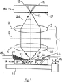
図1は、例えばスキャナ型の装置であってよいマイクロリソグラフィ投影露光装置の投影対物レンズ1の波面測定用装置の概略側面図を示す。ここで、及び図の残りでは、本ケースで重要である測定装置の構成部品だけがそれぞれ示されており、装置は必要に応じてさらに従来の型の構成部品を有してよい。簡単にするために、投影対物レンズ1から、対応するレンズ平面2を備えた入射側レンズ9、開口絞り8、及び対応するレンズ平面3を備えた出射側レンズ10だけが追加の通例の構成部品を表すように示されている。露光装置の有効動作モードでは、ウェハは習慣的な方法で有効な放射線で露光され、その放射線によって投影対物レンズ1はレチクル構造をウェハ上に結像する。このために、レチクルは対物レンズ1の物体平面に導入され、ウェハは対物レンズの像平面内に配置される。紫外線等の放射線は、出射側レンズ11だけが代表的に示されている照明システムにより供給される。通常物体側と呼ばれる対物レンズ1の入射側レンズ9の前の領域はこのようにして対物レンズの有効放射入射側を構成し、通常像側と呼ばれる出射側レンズ10の後部の領域は相応して対物レンズ1の有効放射出射側を構成する。
FIG. 1 shows a schematic side view of a device for measuring the wavefront of a
投影対物レンズ1は、図1に測定動作モードで描かれており、そのために測定装置の構成部品は露光装置に導入される、及び/又は露光装置に統合される。代替策として、測定装置は、対物レンズ1が導入される自律測定ステーションとして設計されてよい。測定装置は、関連するソース側測定構造マスク62を備えた測定放射線ソースと、関連する検出器側測定構造マスク19を備える検出器12とを備え、ソース側測定構造マスク62から出現する測定放射線80を、対物レンズ1を通して、前述の有効動作モードの有効放射線方向に反対方向で、つまり像側、つまり有効放射出射側から物体側、つまり有効放射入射側に通過させることを目的とする。
The
このため、測定放射線ソースは、対物レンズ1の像側に配置され、対物レンズ1に面する全面60でソース側測定構造マスク62を支える測定構造支持材5を有する。測定構造支持材5は、ソース側測定構造マスク62が対物レンズ1の像平面にあるように配置され、測定構造マスク62は伝播中操作され、このために、透明な構造体要素と不透明な構造体要素を測定構造領域4の中に備える測定構造体を有する。
For this purpose, the measurement radiation source has a
検出器12は、対物レンズ1の物体側、つまり有効放射入射側に配置され、対物レンズに面する前面で、入射側検出器素子として検出器側測定構造マスク19を支え、検出器側測定構造マスク19が対物レンズ1の物体平面にあるように配置される検出器支持材83を備える。検出器支持材83は透明の材料からプレート型で形成され、背面に検出器素子16を有する。検出器側測定構造マスク19は、検出器側測定構造領域13を備え、その上に対物レンズ1が、検出器素子16によって検出される干渉又は重ね合せのパターンを生成するために、ソース側測定構造マスク62の測定構造領域4を結像する。つまり、ソース側測定構造領域4から出現する測定放射線80は有効放射線方向に反対の測定放射線方向で対物レンズ1を通過し、次に検出器素子16により検出されるために検出器側測定構造領域13に入射する。
The
測定放射線を提供するために、測定装置は、露光装置の既存の照明システム11を活用し、そのシステムは以後測定放射線ソースの一部となる。このために、検出器側測定構造マスク19は、検出器側測定構造領域13の外部にあるストリップ型の通過領域14を有し、その通過領域は、代わりに別の形を有することもある。その測定構造領域13及びその通過領域14の外部に、検出器側測定構造マスク19は光不透明層17を有する。このようにして、検出器側測定構造領域13の外部のストリップ型領域内では、対物レンズ1を介して測定放射線ソースの測定構造支持材5まで、照明システム11によって生成される放射線80aが検出器支持材83を、特に測定構造マスク19を通過する。ソース側測定構造マスク62には、示されている例ではストリップ型の通過領域であり、対物レンズ1によって生成される検出器支持材通過領域14の像に、形式と位置で対応し、ソース側測定構造領域4の外部にある、対応する通過領域7が備えられる。
In order to provide the measuring radiation, the measuring device takes advantage of the existing
測定構造支持材5は、ウェハの形状に従って、例えば厚さが約1mmのプレート型又は円板型で形成され、その結果それは露光装置のウェハステージを介して導入できる。さらに、測定構造支持材5は、その測定構造マスク62の通過領域7を介して、前面で結合する放射線80aと可能な限り均一に、且つ非干渉に(incoherently)その測定構造マスク62の測定構造領域4を照明するために設計される。このために、測定構造支持材5は光散乱領域、したがって領域全体でのその背面61でビーム偏向層領域6、及び測定構造マスク62の内側で測定構造領域4および通過領域7の外部の前面も備え、その層の領域は、以後測定構造マスク62が前面で作られる、例えば支持材コアの表面を粗くすることによって形成されてよい。外部側面では、測定構造支持材5には適切な光吸収遮断層が、その背面61と測定構造領域4および測定構造マスク62の通過領域7の外部の前面に設けられる。内部では、測定構造支持材5は透明な材料を備える。図1に示されるように、測定構造支持材5のこの構造は結合する放射線80aの複数の反射を生じ、それによりソース側測定構造マスク62の測定構造領域4は、伝播中にその背面から十分に均一に且つ非干渉に照明される。代替実施形態では、測定構造支持材5はこのために異なって構築されてもよく、その場合反射防止膜が付けられた、ミラーコーティングされた、吸収及び/散乱領域が設けられてよい。このためにはマイクロプリズム構造体及び光回折構造体も使用できる。
The
本例では、検出器素子16はCCDアレイとして形成され、相対的に高速な検出を可能にする。CID装置又はCMOS装置等の他のオプトエレクトロニック検出器素子が代替策として考えられる。光化学検出を達成する検出器素子を使用することも可能である。被膜15は、背面の検出器装置16を、照明システム11から入射する放射線の直接的な照射から保護する。
In this example, the
検出器側測定構造マスク19の測定構造領域13が回折格子構造として形成される一方、図1の装置は好ましくは、シヤリング干渉計側技法による波面測定用に設計され、そのためにソース側測定構造マスク62の測定構造領域4は次に、波面ソースにおいてこのために通例的な構造体の1つを有するいわゆる干渉性マスクとして形成される。例えば1:4の投影対物レンズ1の典型的な縮小尺度を考慮すると、回折格子の平面性に関してなされる要件は、その像側位置決め付きの従来の測定装置の事例においてより、例えば16という測定係数分、相応して低くなる。回折格子の構造体は同様に4という係数分、大きく維持することができ、その結果それらはより簡略な装置を使用して作成できる、あるいはマスタオリジナルからの密着印画(contact copy)として優れた品質で安価に複製できる。これは、特にソース側測定構造マスク62の構造体が、結像尺度に対応するサイズの縮小があっても相対的に簡略に製造できるときに特に有利である。検出器側及び/又はソース側の測定構造マスク19、62は、図中で双方向の矢印81、82によって示されるように、移動中の検出器12又は構造支持材5によって測定を実行するために側面方向に変位できる。
While the
図2は、入射側光学素子として働く検出器側測定構造マスク19の好ましい実施例を詳しく示している。この例では、検出器側測定構造マスク19は測定構造領域13の右側と左側で少し離れているストリップ型通過領域14を有する。測定構造領域13はチェック模様の回折格子として形成される。マスク領域の残りは、光不透明層17で覆われる。図示されていない代替の有利な実施形態では、図示されている通過ストリップ14と回折格子ストリップ13のパターンは検出器側測定構造マスク19上で複合的に繰り返されてよい。
FIG. 2 shows in detail a preferred embodiment of the detector-side measuring
図3は光学系の波面測定用の追加の装置の概略側面図を示し、ここで及び以下の例ではその系のために、図1の投影対物レンズ1が再び、本発明による装置によって測定できる任意の他の光学系を表すように検討されている。簡単にするために、全ての図で、同一参照記号は機能的に対応する、必ずしも同一ではない要素のために選ばれ、このような要素の不必要に繰り返される説明は省略されている。図3の装置は検出器12aを有し、その機能はほとんど図2の検出器12の機能に一致する。図2の検出器に関する唯一の相違点は、図3の検出器12aが通過領域を持たないという点である。図3の装置の場合では、測定放射線は、測定放射線ソースの測定構造支持材5aのソース側測定構造マスク62aの前で、側面方向で、つまり投影対物レンズ1の光学軸28に関して交差する方向に発せられる。必要に応じて個別に、又は組み合わせて使用できる1つ又は複数の測定放射線変換装置21、22によって、側面方向で送られる測定放射線は正面から、ソース側測定構造マスク62aのそれぞれの通過領域7a、7bに偏向される。
FIG. 3 shows a schematic side view of an additional device for wavefront measurement of an optical system, here and in the following examples, for that system, the
残りについて、図3の測定構造支持材5aが図1の測定構造支持材5に相当する。図3は、側面方向で送られる測定放射線80b、80cを適切に偏向するための測定放射線変換装置の2つの変形、正確には代替策としてあるいは追加で使用することができ、測定構造支持材5aの前面での1つのカテトス(cathetos)面、及びビーム偏向のためにミラーコーティングされる斜辺面によって支える平面鏡22と直角プリズム21を示している。正のレンズ20はプリズムの第2のカテトス面に固定され、このようにして相対的に小さく保つことができる通過領域7bまで、目標とされるカップリングのための光を、光のビーム経路に相当するレンズ20の焦点距離のために測定構造支持材5aの中に集束するために役立つ。
For the rest, the measurement structure support material 5a in FIG. 3 corresponds to the measurement
図1の例においてのように、露光装置の通例の照明システムは測定放射線ソースの放射線発生装置として働いてよく、このケースでは照明システムによって供給される放射線は図示されていない方法で対物レンズ1の前で外部結合されてから、測定構造マスク62aの前で側面方向で送られる。代替策として、自律測定放射線発生装置が使用されてよく、その場合、例えば対物レンズ位置合わせのための測定装置において通例であるように、相対的に簡略で費用効果の高い放射線発生装置が対物レンズ測定には十分である可能性がある。測定構造支持材5aは、図3の交差した両方向矢印84によって象徴されるように、シヤリング干渉計側技法の間の側面方向変位のために、ウェハステージ又は変位装置23で適用される。
As in the example of FIG. 1, the usual illumination system of the exposure apparatus may act as a radiation generator of the measurement radiation source, in which case the radiation supplied by the illumination system is not shown in the manner of the
図4は、図3で代わりに使用することができ、前面に結合する光を備える測定放射線ソースの概略側面図を示している。図4の測定放射線ソースは、それが表側の結合可能な表面では透明であり、側面方向に送られる測定放射線80b、80cがそこに直接的に結合するという事実により、本質的に図3のものとは異なる測定構造支持材5bを備える。優れた結合可能性のために、2つの表側測定放射線誘導装置20a、24が示され、代わりにその内の一方又は両方が設けられてよい。この種の第1の装置は結合可能な表面に導かれる光導波管24として形成され、第2の装置は集束物体として結合可能な面に取り付けられる正のレンズ20aによって形成される。両方の装置20a、24とも測定放射線を測定構造支持材5bの内部に側面方向で結合し、それは、後部から均一に測定構造領域4を照明するために、散乱面又は偏向面6で繰り返し反射され、回折され、及び/又は散乱される。この例では、測定構造領域4は、さもなければ光不透明ソース側測定構造マスク62b上で形成される。
FIG. 4 shows a schematic side view of a measurement radiation source that can be used instead in FIG. The measuring radiation source of FIG. 4 is essentially that of FIG. 3 due to the fact that it is transparent on the front-side connectable surface and the measuring radiation 80b, 80c sent in the lateral direction is directly coupled there. The measurement structure support material 5b different from that is provided. For superior coupling possibilities, two front-side measuring
図5は、表側で結合する光を備える測定放射線ソースの変形の概略側面図を示している。この例では、測定放射線は正のレンズ20aを通して表側で測定構造支持材5cの中に結合され、その測定構造支持材は、図4のものとは対照的に、内部に取り付けられ、ビーム偏向装置として働く直角プリズム25を有し、測定構造領域4はプリズムの正面カテトス面に位置している。プリズム25の斜辺面は、複数の反射、回折及び/又は散乱の後に、適切な場合は、測定構造領域4に対し、表側で発せられる測定放射線を偏向する偏向面63として形成される。偏向面63は、散乱様式及び/又は反射様式で実現されてよい。
FIG. 5 shows a schematic side view of a variant of a measurement radiation source with light coupling on the front side. In this example, measurement radiation is coupled into the measurement structure support 5c on the front side through a
この際、図3から図5に図示されている側面方向の放射線を送り、及びこのために適した測定構造支持材も、原則的に、従来のように物体側に配置される測定構造マスクのために使用できることが言及されなければならない。 At this time, the radiation in the lateral direction shown in FIGS. 3 to 5 is sent, and the measurement structure support material suitable for this is also used in principle for the measurement structure mask arranged on the object side as in the prior art. It must be mentioned that it can be used for.
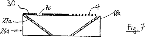
図6は、測定放射線ソース用の測定構造支持材5dの追加の変形の概略側面図を示しており、測定放射線80aは前面で支持材の中に結合され、支持材は2つのビーム偏向素子27、28を備える測定放射線変換装置26を有する。測定放射線は、図1の場合でのように、例えば露光装置の照明システムによって供給されてよい。測定構造支持材5dはその前面に、測定放射線を結合するための通過領域7cを備え、そこから少し離れて、測定構造領域4を備える測定構造マスク30を有する。測定構造支持材5dの内部では、通過領域7cの下に、対物レンズの光学軸28を基準にして45°で傾けられたビーム偏向領域27を備える第1のビーム偏向素子27が取り付けられている。この場合では、ビーム偏向素子27は、ミラーコーティングされた斜辺面を有する、図5のようなプリズムとして、あるいは単純な鏡として実施されてよく、それが第2のビーム偏向素子18に衝突する前に、前部及び背部の散乱層領域及び/又は反射層領域6のある測定構造支持材5dの隣接する領域に測定放射線を反射する。後者は第1ビーム偏向素子27のように形成されてよい。第2のビーム偏向要素18の反射面は同様に、光学対物レンズ軸28に関して45°傾斜し、測定構造領域4に測定放射線を偏向する。
FIG. 6 shows a schematic side view of an additional variant of the
図7から図9は前述の基本的な構造を備えた、図6の測定放射線変換装置26の考えられる変形を示している。それらは、ビーム経路に散乱素子及び/又は集束素子がどのようにして導入されるのかによってのみ異なる。図7に示される放射線変換装置26aのケースでは、第1の及び第2のビーム偏向素子が、さらに光散乱面を備える、それぞれ偏向鏡27a、18aの形で実現されている。図8は、それぞれ偏向鏡の形を取る第1のビーム偏向素子と第2のビーム偏向素子27、18の間に設けられる散乱横断方向壁構造39を備える測定放射線変換装置26bを示す。図9は測定放射線変換装置26cを描いており、その場合では、第2のビーム偏向素子18aがさらに散乱表面を有し、第1のレンズ37が第1のビーム偏向素子27の前の光経路内に位置し、第2のレンズ38が第2のビーム偏向素子18aである光路内に位置する。両方のレンズとも測定構造マスク30の平面に平行な平面内にあり、ビーム整形光学部品として働く。この例示的な実施形態で非常に高い発光効率が達成できる。
7 to 9 show possible variants of the measuring radiation conversion device 26 of FIG. 6 with the basic structure described above. They differ only in how the scattering and / or focusing elements are introduced in the beam path. In the case of the radiation conversion device 26a shown in FIG. 7, the first and second beam deflecting elements are realized in the form of deflecting
図6から図9に示されている測定放射線変換装置26、26a、26b、26cは、擬似モノリシックな(quasi-monolithic)機能単位として高い精度で製造することができ、個別にあるいはグループで測定構造支持材5dの中に挿入できる。ビーム偏向領域及び追加のビーム整形素子は結合する放射線の最適活用のために適した方法でコーティングされてよい、及び/又はパターン化されてよい。光は好ましい方向で目標とされたように偏向されるため、2つのビーム偏向領域による偏向は特に効率的である。
The measuring
図10は、反射として働くソース側測定構造マスク41と、測定放射線誘導装置42を備える測定放射線ソースを備える対物レンズ1等の光学結像系の波面測定用の追加の改良された装置の概略側面図を示している。装置は物体側で図3の検出器12aを有する。反射として働くソース側測定構造マスク41は、対物レンズ1の像平面内に配置され、測定のために変位装置23によって側面方向で変位できる測定構造支持材40上に取り付けられる。測定放射線誘導装置42はこの場合では反射面として形成され、ビーム発生装置(不図示)から側面方向で送られる放射線をソース側測定構造マスク41上に偏向する。測定放射線誘導装置42には、さらに集束効果及び/又は散乱効果がある。さらに、反射又は伝播中に操作されるゾーンプレートは、照明放射線を集束するために使用されてよく、EUV放射線等の短波放射線のケースで特に有利である。さらに、放射線が測定放射線誘導装置42に狭い入射角で衝突し、その結果、それが全反射の活用で偏向されると有利である。ソース側測定構造マスク41の測定構造領域43は、照明光を散乱する第1の構造領域44と、照明光を反射又は吸収する第2の構造領域43を有する。測定放射線80が測定される対物レンズ1に移動するのは、第1の散乱構造領域44からだけである。第2の構造領域43は、対物レンズ1の開口角より大きい角度で放射線が反射されるように、照明放射線を吸収するか、あるいは後者が入射角で第2の構造領域に衝突するかのどちらかである。
FIG. 10 shows a schematic side view of an additional improved apparatus for wavefront measurement of an optical imaging system such as an
図11は、レチクルのように構築され、電子部品50を備える検出器12bの概略側面図を示す。検出器12bは、測定される対物レンズの照明システム11と入射側レンズ9の間に配置される。検出器12bは検出器支持材51を有し、検出器側測定構造マスク19aは測定構造領域13と、対物レンズに面する検出器支持材のその側端に設けられている通過領域14を備える。検出器12bの機能に関して図1の説明を参照しなければならない。照明システム11に面する側では、検出器12bが、照明システム11及び電子部品50からの直接的な放射線に対する遮蔽15aと、図11に示されているように放射線に敏感な検出器素子16aに沿って平坦な設計で実現される電子部品50とともに、CCDアレイ又はフラットイメージ記録カメラ装置等の検出器素子16aも有する。電子部品は、例えば内蔵電源、遠隔データ伝送用データ回線、及び検出器素子の測定信号を評価するための評価装置も備えてよい。内部電源は例えば電池、充電式電池、又は太陽電池装置等の電流発生装置であってよい。
FIG. 11 shows a schematic side view of a detector 12b constructed like a reticle and comprising an
図12は、石英支持材51a上の本発明による測定装置で使用できる検出器12cの追加例の概略側面図を示す。検出器12cに関して、図1と図11の説明を参照する必要がある。図11に示されている検出器12bと対照的に、検出器12cは、対物レンズに面する側端で、測定構造領域13を備えるが、通過領域のない測定構造マスク19bを有している。したがって検出器12cは、例えば図3の装置で使用するのに適している。電子構成部品50と検出器素子16aと遮蔽15aも石英支持材51aの内部に取り付けられている。石英支持材51a内の電子回路基板52は電子部品用の支持材として働く。
FIG. 12 shows a schematic side view of an additional example of a detector 12c that can be used in the measuring device according to the invention on a quartz support 51a. Regarding the detector 12c, it is necessary to refer to the description of FIG. 1 and FIG. In contrast to the detector 12b shown in FIG. 11, the detector 12c has a measurement structure mask 19b with a
図13は、点回折干渉技法(PDI:point diffraction interferometry)によって、対物レンズ1等の光学結像系の波面測定用の追加装置の概略側面図を示す。図13の装置は物体側に検出器12dを有し、検出器の構成は図11の構成に大いに対応し、PDI検出構造体13aを備える改良された検出器側測定構造マスク19cが提供されている。図6の様式であるが、改良された検出器側測定構成マスク62cおよび図9の様式での測定放射線変換装置26d、及びビーム分割回折格子84も備えるソース側測定構造支持材5eは像側に配置される。装置の機能のために、図1、図6、及び図9に関して前述の記述が当てはまり、ピンホールが測定構造支持材5eのソース側測定構造マスク62cの測定構造領域4aとして使用され、図13に示されるように、ピンホール構造体4aから出現する波面は、回折格子84によって、テスト試験波(test speciman wave)80dの通過のためにPDI検出構造体13aの第1の大きな方の開口部に衝突するテスト試験波80d(実線)と、ここで回折されるためにPDI検出構造体13aの第2の小さい方のピンホール開口部に衝突する基準電波80e(破線)とに分割される。シヤリング干渉計測技法のケースでのように、測定される対物レンズ1の収差特性は、透過されたテスト試験波と、検出器素子16aで回折された基準波(reference wave)の間の干渉パターンから推定できる。
FIG. 13 shows a schematic side view of an additional device for wavefront measurement of an optical imaging system such as the
例示的な実施形態によって明らかにされたように、本発明による装置は特にマイクロリソグラフィ投影露光装置の投影対物レンズの測定に使用されてよく、図1に示されているシヤリング干渉計測技法、図13に示されている点回折干渉技法、モアレ技法又は例えばハートマン(Hartman)又はシャックーハートマン型の波面測定技法等の他の従来の波面測定技法を使用できる。本発明が、有効放射線方向に関して逆の測定放射線方向を使用することについて特に有利なことは、ウェハ平面の近傍では、ウェハ状の薄いソース側測定構造支持材を空間を節約するようにそこに配置できるには直ちに十分であるが、限られた構造上の空間だけが使用可能であるのに対し、物体側ではレチクル平面の近傍に、相対的に構造空間集約型(structural-space-intensive)検出器にとって十分な構造上の空間があるという点である。 As demonstrated by the exemplary embodiment, the apparatus according to the invention may be used in particular for the measurement of the projection objective of a microlithographic projection exposure apparatus, the shearing interferometry technique shown in FIG. Other conventional wavefront measurement techniques such as the point diffraction interferometry technique, the moire technique shown in Figure 1 or the Hartman or Shack-Hartmann type wavefront measurement technique can be used. Particularly advantageous for the present invention to use a measurement radiation direction that is opposite to the effective radiation direction is that in the vicinity of the wafer plane, a wafer-like thin source-side measurement structure support is placed there to save space. While it is immediately sufficient to do, only limited structural space can be used, whereas on the object side, relatively structural-space-intensive detection is located near the reticle plane. There is sufficient structural space for the vessel.
検出器の電子部品からの発熱の問題も、検出器の廃熱が上昇し、したがって考えられる熱放射効果は別として検出器の発熱が根本的な投影対物レンズの結像特性に悪影響を及ぼさないために、削減される。検出器とその測定構造支持材付きの測定放射線ソースの両方ともマイクロリソグラフィ投影露光装置に統合できる、あるいは自律装置として構成できる。必須であるのは、それらが波面測定を実施するために投影対物レンズのビーム経路の中に導入可能であり、測定の終結の後にビーム経路から取り除くことができるという点である。代替策として、投影対物レンズ又は測定される他の光学系を測定のために持ち込むことができる別の測定ステーションとして測定装置を構築することも可能である。 The problem of heat generation from the detector electronics also increases the waste heat of the detector, so that apart from possible thermal radiation effects, the heat generation of the detector does not adversely affect the imaging characteristics of the underlying projection objective In order to be reduced. Both the detector and the measuring radiation source with its measuring structure support can be integrated into the microlithographic projection exposure apparatus or configured as an autonomous device. What is essential is that they can be introduced into the beam path of the projection objective to perform wavefront measurements and can be removed from the beam path after the end of the measurement. As an alternative, it is also possible to construct the measuring device as a separate measuring station where a projection objective or other optical system to be measured can be brought in for measurement.
本発明はさらに浸漬液を使用する光学測定を実行する可能性を備え、そのために後者は特に測定放射線ソース内に、及び/又は後者の近傍に、及び/又は検出器内に及び/又は後者の近傍に導入されてよい。これは、例示的な様式で、及び3つの例に基づいた追加の考えられる実現を表す方法で説明される。 The invention further provides the possibility to carry out optical measurements using immersion liquid, for which reason the latter is in particular in the measuring radiation source and / or in the vicinity of the latter and / or in the detector and / or in the latter It may be introduced in the vicinity. This is illustrated in an exemplary manner and in a way that represents additional possible implementations based on three examples.
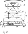
したがって、図14は、浸漬液応用例は別にして、その他について参照されてよく、同一の参照記号が同一の又は機能上同等な要素について使用される図1の装置に対応する装置変形を示している。図14は、出射側で平面的な終端プレート10’で終端する投影対物レンズ1’のための測定動作モードを示しており、その場合では終端する投影対物レンズ要素は、代わりにレンズ要素等の何らかの他の光学部品であってもよい。対物レンズ1’の終端要素10’と以後の測定構造支持材5’の間の空間90は、ベローズ型シール等の円周シール91を使用する浸漬液チャンバとして形成される。浸漬液は、矢印によって示されるように、入口92を介してチャンバ内に送り込むことができる。入口92の反対側では、浸漬液が浸漬液チャンバ90から出口93を介して放出される。示されている例では、入口線路と出口線路92、93がそのそれぞれの表側で測定構造支持材5’を貫通する。浸漬液チャンバ90を浸漬液で充填し、次にその中に後者を保持する、あるいは代わりに浸漬液チャンバ90を通る連続浸漬液の流れを維持するために必要に応じて準備がされてよい。任意で、浸漬液チャンバ90の外部又は内部での浸漬液の温度を制御するための手段が設けられる。この目的のため、例えば測定構造支持材5’に統合される等、温度を測定するための、及び必要な場合には、浸漬液の温度を調整するための手段もあってよい。
Accordingly, FIG. 14 shows an apparatus variant corresponding to the apparatus of FIG. 1 that may be referred to elsewhere, aside from immersion liquid applications, where the same reference symbols are used for the same or functionally equivalent elements. ing. FIG. 14 shows a measurement mode of operation for a
測定構造支持材5’は、図1の例でのように透明な材料を備えてよい、あるいは代わりにその前面60とその背面61の間の空洞94の構造で形成されてよく、次にその空洞の中に浸漬液が同様に導入できる。このために、測定構造支持材5’の空洞94は、共通の浸漬液チャンバを形成するために、必要に応じて、対物レンズ1’と測定構造支持材5’の間の浸漬液チャンバ90と流体接続してよい、あるいはこれとは別個に第2の浸漬液流体チャンバを形成してよい。浸漬液の使用には公知の優位点がある。特に、対物レンズ1’の像側から測定構造領域4と試験される対物レンズ1’の非常に高開口の照明を提供することができる。
The
図15は、試験される光学系の出射側要素10と測定構造支持材5bの間の空間96が、ベローズ型シール等の円周シール95によって浸漬液チャンバとして形成される図4の測定構造支持材5bの装置のための実現変形を相応して示す。適切な浸漬液は、通例の手段(特に図示されず)によってチャンバ内に導入できる。浸漬液に関連する追加の測定、及びそれで達成される特性の優位点に関して、図14に関してになされた記述は、参照してよい図15で明示的に説明されていない同じように当てはまる。
15 shows the measurement structure support of FIG. 4 in which a space 96 between the
残りに関しては図13に関する記述を参照してよいが、この点で同一の参照記号が使用される一方で、図16は、図13からの装置の浸漬液の変形を示し、その場合再び浸漬液に関連する変型だけがこの際に説明される必要がある。図16の例では、試験される対物レンズ1の出射側部品10と、測定構造支持材5eの間の空間97が、ベローズ型シール等の円周シール28を使用して再び浸漬液チャンバとして形成される。これと関連して、連続流体として等、浸漬液を送り込み、放出するための手段、及び必要な場合、流体温度を測定し、調節するための手段が準備される。この点で、及び追加の考えられる変型、浸漬液を使用する優位点及び特性に関して、図14と図15に関する記述を、及び序論で言及された従来の技術を参照してよい。
For the rest, reference may be made to the description with respect to FIG. 13, but the same reference symbols are used in this respect, while FIG. 16 shows a variation of the immersion liquid of the device from FIG. Only variants related to need to be described at this time. In the example of FIG. 16, the
浸漬液を導入するための手段も、図示され、前述の残りの例示的な実施形態について同様に設けられ当てよいことは言うまでもない。さらに、このような手段は図14から図16に関して前述のような測定放射線ソースでの存在に加えて、及び存在に対する代替策として、検出器側で同じように設けられてよい。すなわち、浸漬液は、検出器支持材又は後者と試験される光学系の間の空間の中に等、検出器構成部品の中に、あるいはその近傍に類似するように導入でき、さらに詳細な説明を必要としない。 It will be appreciated that means for introducing the immersion liquid are also shown and similarly provided for the remaining exemplary embodiments described above. Furthermore, such means may be provided in the same way on the detector side in addition to and as an alternative to the presence at the measurement radiation source as described above with reference to FIGS. That is, the immersion liquid can be introduced in or similar to the detector component, such as in the space between the detector support or the latter and the optical system being tested, and more detailed description. Do not need.
Claims (24)
測定放射線を前記結像光学系(1)に放射する少なくとも1つのソース側測定構造マスク(62、62a〜62c、41)を前記結像光学系(1)の前記有効放射出射側に配置可能な測定放射線ソース(5、5a〜5e、40、11)と、
前記結像光学系(1)から生じる測定放射線を受け取る少なくとも1つの検出器側測定構造マスク(19、19a〜19c)を前記結像光学系(1)の前記有効放射入射側に配置可能な検出器(12、12a〜12d)と、を備え、
前記測定放射線ソース(5、5a〜5e、40、11)は、前記有効放射出射側での位置決めのための前記ソース側測定構造マスク(62、62a〜62c、41)を備え、及び/又は、前記検出器(12、12a〜12d)は、前記有効放射入射側での位置決めのための前記検出器側測定構造マスク(19、19a〜19c)を備え、
前記検出器(12、12a〜12d)は、前記検出器側測定構造マスク(19、19a〜19c)、及び/又は、前記ソース側測定構造マスク(62、62a〜62c、41)により生成された、干渉パターン又は重ね合わせパターンを検出する
ことを特徴とする装置。 Effective emitting body to propagate effective radiation was irradiated at the incident side, a device for optically measuring an imaging optical system (1) used to image the active radiation emission side,
At least one source-side measurement structure mask (62, 62a to 62c, 41) that radiates measurement radiation to the imaging optical system (1) can be arranged on the effective radiation exit side of the imaging optical system (1). A measuring radiation source (5, 5a to 5e, 40, 11);
Said image forming optical system (1) receives the measurement radiation originating from at least one detector-side measurement structure mask (19,19A~19c) said positionable effective radiation entrance side detects the image forming optical system (1) Vessel (12, 12a-12d),
The measurement radiation source (5, 5a to 5e, 40, 11) comprises the source side measurement structure mask (62, 62a to 62c, 41) for positioning on the effective radiation exit side, and / or It said detector (12,12a~12d) comprises the detector-side measurement structure mask for positioning in the effective radiation entrance side (19,19a~19c),
The detector (12, 12a to 12d) is generated by the detector side measurement structure mask (19, 19a to 19c) and / or the source side measurement structure mask (62, 62a to 62c, 41). , and wherein that you detect an interference pattern or overlapping patterns.
前記ソース側測定構造マスクは透明な構造体要素と不透明な構造体要素を有し、
前記測定放射線ソースは、前記ソース側測定構造マスクの上流にある前記測定放射線のビーム経路内に測定放射線変換装置(6、26、26a〜26c)を備えることを特徴とする請求項1に記載の装置。The measurement radiation source is designed for backlighting of the source side measurement structure mask;
The source side measurement structure mask has a transparent structure element and an opaque structure element ;
The measurement radiation source comprises a measurement radiation conversion device (6, 26, 26a-26c) in the beam path of the measurement radiation upstream of the source side measurement structure mask. apparatus.
前記透明な支持体本体は、
透明な構造体要素と不透明な構造体要素を持ち、且つ測定構造領域(4、4a)を持つ測定構造マスク(62、62a〜62c)を、前記透明な支持体本体の、前記結像光学系(1)側の面上に有し、及び、前記測定構造領域(4、4a)を前記有効放射出射側から照明するための測定放射線変換装置(6、26、26a〜26c)を内部に有し、
該透明な支持材本体の中に測定放射線を通過させる通過領域は、前記面上にて、前記測定構造マスク(62、62a〜62c)の前記測定構造領域(4、4a)の外側に配置される、
ことを特徴とする、請求項2〜5又は8〜11のずれか一項に記載の装置で使用するための測定構造支持材。 A measurement structure support comprising a transparent support body,
The transparent support body is
A measurement structure mask (62, 62a to 62c) having a transparent structure element and an opaque structure element and having a measurement structure region (4, 4a) is used as the imaging optical system of the transparent support body. (1) A measurement radiation conversion device (6, 26, 26a to 26c) for illuminating the measurement structure region (4, 4a) from the effective radiation emission side is provided inside. And
A passage region for allowing measurement radiation to pass through the transparent support body is arranged on the surface outside the measurement structure region (4, 4a) of the measurement structure mask (62, 62a to 62c). The
Characterized in that, measured structural support for use in the apparatus according to the deviation of the claims 2-5 or 8-11.
測定放射線ソースのソース側測定構造マスクを前記有効放射出射側に配置し、及び/又は、検出器の検出器側測定構造マスクを前記有効放射入射側に配置するステップと、
前記測定放射線ソースにより提供される測定放射線を前記有効放射出射側の前記結像光学系に放射するステップと、
前記測定放射線を検出するために前記有効放射入射側で前記結像光学系から生じる測定放射線を受け取るステップと、
前記検出器側測定構造マスク、及び/又は、前記ソース側測定構造マスクにより生成された、干渉パターン又は重ね合わせパターンを検出するステップと
を備える方法。 Effective radiation entrance side object to propagate effective radiation by irradiating with a method for optical measurement of the imaging optical system used to image the active radiation emission side, the measurement by measurement radiation To implement
Placing a source side measurement structure mask of a measurement radiation source on the effective radiation exit side and / or placing a detector side measurement structure mask of a detector on the effective radiation entrance side;
Radiating measurement radiation provided by the measurement radiation source to the imaging optics on the effective radiation exit side;
Receiving a measurement radiation resulting from said imaging optical system in the effective radiation entrance side in order to detect the measuring radiation,
Detecting an interference pattern or an overlay pattern generated by the detector side measurement structure mask and / or the source side measurement structure mask .
Applications Claiming Priority (3)
| Application Number | Priority Date | Filing Date | Title |
|---|---|---|---|
| DE102004003585.7 | 2004-01-16 | ||
| DE102004003585 | 2004-01-16 | ||
| PCT/EP2005/000184 WO2005069080A2 (en) | 2004-01-16 | 2005-01-12 | Device and method for the optical measurement of an optical system, measurement structure support, and microlithographic projection exposure apparatus |
Publications (2)
| Publication Number | Publication Date |
|---|---|
| JP2007518257A JP2007518257A (en) | 2007-07-05 |
| JP4782019B2 true JP4782019B2 (en) | 2011-09-28 |
Family
ID=34778111
Family Applications (1)
| Application Number | Title | Priority Date | Filing Date |
|---|---|---|---|
| JP2006548246A Expired - Fee Related JP4782019B2 (en) | 2004-01-16 | 2005-01-12 | Apparatus and method for optical measurement of optical system, measurement structure support, and microlithography projection exposure apparatus |
Country Status (4)
| Country | Link |
|---|---|
| US (1) | US8004690B2 (en) |
| EP (1) | EP1704445A2 (en) |
| JP (1) | JP4782019B2 (en) |
| WO (1) | WO2005069080A2 (en) |
Families Citing this family (13)
| Publication number | Priority date | Publication date | Assignee | Title |
|---|---|---|---|---|
| WO2005069080A2 (en) * | 2004-01-16 | 2005-07-28 | Carl Zeiss Smt Ag | Device and method for the optical measurement of an optical system, measurement structure support, and microlithographic projection exposure apparatus |
| US7518703B2 (en) * | 2005-06-28 | 2009-04-14 | Asml Netherlands B.V. | Lithographic apparatus and method |
| JP2007081390A (en) * | 2005-08-17 | 2007-03-29 | Nikon Corp | Device for observation, device for measurement, device for exposure and method for exposure, method for producing device, substrate for producing device and device for positioning |
| DE102005041203A1 (en) * | 2005-08-31 | 2007-03-01 | Carl Zeiss Sms Gmbh | Device for interferometric measurement of phase masks used for e.g. lithography, produces phase shifting interferogram to be applied over phase mask by translating coherence mask and/or diffraction grating in X-Y direction |
| CN101833235B (en) | 2009-03-13 | 2012-11-14 | 中芯国际集成电路制造(上海)有限公司 | Quality detection system and method for original mask copy |
| EP2264528A1 (en) * | 2009-06-19 | 2010-12-22 | ASML Netherlands B.V. | Sensor and lithographic apparatus |
| CN102243444B (en) | 2010-05-14 | 2013-04-10 | 北京京东方光电科技有限公司 | Exposure equipment, mask plate and exposure method |
| DE102010041556A1 (en) * | 2010-09-28 | 2012-03-29 | Carl Zeiss Smt Gmbh | Projection exposure apparatus for microlithography and method for microlithographic imaging |
| DE102012204704A1 (en) * | 2012-03-23 | 2013-09-26 | Carl Zeiss Smt Gmbh | Measuring device for measuring an imaging quality of an EUV objective |
| DE102017203376B3 (en) * | 2017-03-02 | 2018-05-24 | Carl Zeiss Smt Gmbh | Measuring device and method for measuring a wavefront error of an imaging optical system and a projection exposure apparatus for microlithography |
| DE102018204626A1 (en) * | 2018-03-27 | 2019-04-04 | Carl Zeiss Smt Gmbh | Illumination mask and method for its production |
| DE102018124396A1 (en) * | 2018-10-02 | 2020-04-02 | Carl Zeiss Smt Gmbh | Metrology system and method for measuring an excitation laser beam in an EUV plasma source |
| DE102019100920B4 (en) * | 2019-01-15 | 2020-07-30 | Nedinsco B.V. | Viewing device |
Citations (6)
| Publication number | Priority date | Publication date | Assignee | Title |
|---|---|---|---|---|
| JPS61202432A (en) * | 1985-03-06 | 1986-09-08 | Canon Inc | Projection exposure apparatus |
| JPS6243128A (en) * | 1985-08-20 | 1987-02-25 | Nippon Kogaku Kk <Nikon> | Projecting optical apparatus |
| JPH10289865A (en) * | 1997-04-11 | 1998-10-27 | Nikon Corp | Projection exposing device and method therefor |
| WO1999060361A1 (en) * | 1998-05-19 | 1999-11-25 | Nikon Corporation | Aberration measuring instrument and measuring method, projection exposure apparatus provided with the instrument and device-manufacturing method using the measuring method, and exposure method |
| JP2000195782A (en) * | 1998-12-28 | 2000-07-14 | Canon Inc | Projector and aligner |
| JP2005129557A (en) * | 2003-10-21 | 2005-05-19 | Nikon Corp | Aberration measurement device, aligner, aberration measurement method, exposure method, and device manufacturing method |
Family Cites Families (25)
| Publication number | Priority date | Publication date | Assignee | Title |
|---|---|---|---|---|
| US5978085A (en) * | 1997-03-07 | 1999-11-02 | Litel Instruments | Apparatus method of measurement and method of data analysis for correction of optical system |
| US6819414B1 (en) | 1998-05-19 | 2004-11-16 | Nikon Corporation | Aberration measuring apparatus, aberration measuring method, projection exposure apparatus having the same measuring apparatus, device manufacturing method using the same measuring method, and exposure method |
| TW550377B (en) * | 2000-02-23 | 2003-09-01 | Zeiss Stiftung | Apparatus for wave-front detection |
| DE10105958A1 (en) | 2001-02-09 | 2002-09-12 | Fraunhofer Ges Forschung | Device for anisotropic light scattering and method for producing the device |
| JP4921644B2 (en) | 2001-02-27 | 2012-04-25 | オリンパス株式会社 | Wavefront measuring apparatus and wavefront measuring method |
| JP2005522871A (en) * | 2002-04-15 | 2005-07-28 | カール・ツァイス・エスエムティー・アーゲー | Interference measuring apparatus and projection exposure apparatus comprising the measuring apparatus |
| JP2004061515A (en) * | 2002-07-29 | 2004-02-26 | Cark Zeiss Smt Ag | Method and device for determining influence onto polarization state by optical system, and analyzer |
| DE10261775A1 (en) | 2002-12-20 | 2004-07-01 | Carl Zeiss Smt Ag | Device for the optical measurement of an imaging system |
| US7268891B2 (en) * | 2003-01-15 | 2007-09-11 | Asml Holding N.V. | Transmission shear grating in checkerboard configuration for EUV wavefront sensor |
| JP4314040B2 (en) * | 2003-03-05 | 2009-08-12 | キヤノン株式会社 | Measuring apparatus and method |
| DE10316123A1 (en) * | 2003-04-04 | 2004-10-14 | Carl Zeiss Smt Ag | Phase difference interferometry system for wave front measurement for optical imaging system uses mask structure on object side and grating structure on image side |
| WO2004090490A1 (en) * | 2003-04-11 | 2004-10-21 | Carl Zeiss Smt Ag | Diffuser, wavefront source, wavefront sensor and projection lighting facility |
| AU2003233318A1 (en) * | 2003-05-12 | 2004-11-26 | Carl Zeiss Smt Ag | Optical measuring device and operating method for an optical imaging system |
| WO2005069080A2 (en) * | 2004-01-16 | 2005-07-28 | Carl Zeiss Smt Ag | Device and method for the optical measurement of an optical system, measurement structure support, and microlithographic projection exposure apparatus |
| JP4387834B2 (en) * | 2004-02-27 | 2009-12-24 | キヤノン株式会社 | Point diffraction interferometer, and exposure apparatus and method using the same |
| JP2005311080A (en) * | 2004-04-21 | 2005-11-04 | Canon Inc | Measuring instrument and aligner therewith |
| KR101257960B1 (en) * | 2004-06-04 | 2013-04-24 | 칼 짜이스 에스엠테 게엠베하 | System for measuring the image quality of an optical imaging system |
| DE102005026628A1 (en) * | 2004-06-04 | 2005-12-29 | Carl Zeiss Smt Ag | Telecenter determination device for microlithography-projection illumination system, has processor unit for determining telecenter error value from wave front tip measuring value that is attained by wave front measuring device |
| JP2006324311A (en) * | 2005-05-17 | 2006-11-30 | Canon Inc | Wavefront aberration measuring device and exposing device therewith |
| JP2009283635A (en) * | 2008-05-21 | 2009-12-03 | Canon Inc | Measurement apparatus, measurement method, exposure apparatus, and device manufacturing method |
| JP2010016057A (en) * | 2008-07-01 | 2010-01-21 | Canon Inc | Measuring method, measuring apparatus, exposure apparatus, exposure method, manufacturing method of device and design method |
| JP2010034319A (en) * | 2008-07-29 | 2010-02-12 | Canon Inc | Method for measuring wavefront aberration |
| JP5129702B2 (en) * | 2008-09-17 | 2013-01-30 | キヤノン株式会社 | Measuring apparatus, exposure apparatus, and device manufacturing method |
| JP2010109160A (en) * | 2008-10-30 | 2010-05-13 | Canon Inc | Measuring instrument, exposure device and method of manufacturing device |
| JP5522944B2 (en) * | 2009-01-09 | 2014-06-18 | キヤノン株式会社 | Measuring apparatus, measuring method and exposure apparatus |
-
2005
- 2005-01-12 WO PCT/EP2005/000184 patent/WO2005069080A2/en active Application Filing
- 2005-01-12 EP EP05700815A patent/EP1704445A2/en not_active Withdrawn
- 2005-01-12 JP JP2006548246A patent/JP4782019B2/en not_active Expired - Fee Related
- 2005-01-12 US US10/585,402 patent/US8004690B2/en not_active Expired - Fee Related
Patent Citations (6)
| Publication number | Priority date | Publication date | Assignee | Title |
|---|---|---|---|---|
| JPS61202432A (en) * | 1985-03-06 | 1986-09-08 | Canon Inc | Projection exposure apparatus |
| JPS6243128A (en) * | 1985-08-20 | 1987-02-25 | Nippon Kogaku Kk <Nikon> | Projecting optical apparatus |
| JPH10289865A (en) * | 1997-04-11 | 1998-10-27 | Nikon Corp | Projection exposing device and method therefor |
| WO1999060361A1 (en) * | 1998-05-19 | 1999-11-25 | Nikon Corporation | Aberration measuring instrument and measuring method, projection exposure apparatus provided with the instrument and device-manufacturing method using the measuring method, and exposure method |
| JP2000195782A (en) * | 1998-12-28 | 2000-07-14 | Canon Inc | Projector and aligner |
| JP2005129557A (en) * | 2003-10-21 | 2005-05-19 | Nikon Corp | Aberration measurement device, aligner, aberration measurement method, exposure method, and device manufacturing method |
Also Published As
| Publication number | Publication date |
|---|---|
| WO2005069080A2 (en) | 2005-07-28 |
| EP1704445A2 (en) | 2006-09-27 |
| US8004690B2 (en) | 2011-08-23 |
| US20090116036A1 (en) | 2009-05-07 |
| WO2005069080A3 (en) | 2005-12-08 |
| JP2007518257A (en) | 2007-07-05 |
Similar Documents
| Publication | Publication Date | Title |
|---|---|---|
| JP4782019B2 (en) | Apparatus and method for optical measurement of optical system, measurement structure support, and microlithography projection exposure apparatus | |
| JP4373987B2 (en) | Sensors used in lithographic apparatus | |
| US7528966B2 (en) | Position detection apparatus and exposure apparatus | |
| KR100650946B1 (en) | Radiation system, lithographic apparatus, device manufacturing method and device manufactured thereby | |
| US9645503B2 (en) | Collector | |
| US9939730B2 (en) | Optical assembly | |
| JP2004040067A (en) | Method of detecting focus and imaging system having focus detecting system | |
| TW201042404A (en) | Level sensor arrangement for lithographic apparatus and device manufacturing method | |
| US9709494B2 (en) | Measuring arrangement for measuring optical properties of a reflective optical element, in particular for microlithography | |
| JP2004289116A (en) | Lithographic apparatus and measurement system | |
| JPH11504443A (en) | Lighting unit for optical devices | |
| WO2006126444A1 (en) | Sensor calibration method, exposure method, exposure device, device fabrication method, and reflection type mask | |
| TW504570B (en) | Apparatus and method of determining the reflectance of component light | |
| JPH11251226A (en) | X-ray projection aligner | |
| TW200921284A (en) | Exposure apparatus and semiconductor device fabrication method | |
| JP2001244194A (en) | Abbe arm correction system used in lithography system | |
| KR20240027641A (en) | Apparatus and method for characterizing a microlithographic mask | |
| JP2004246343A (en) | Catoptric system and exposure device | |
| US7081956B1 (en) | Method and device for determining reflection lens pupil transmission distribution and illumination intensity distribution in reflective imaging system | |
| KR20130069660A (en) | Illumination system of a microlithographic projection exposure apparatus | |
| TW201013326A (en) | Exposure apparatus and method of manufacturing device | |
| JP2003295459A (en) | Aligner and exposing method | |
| JP2003257846A (en) | Light source unit, lighting system, and system and method for exposure | |
| US20240061328A1 (en) | Method and apparatus for characterization of a microlithography mask | |
| KR20230150277A (en) | Optical systems specifically for EUV lithography |
Legal Events
| Date | Code | Title | Description |
|---|---|---|---|
| A621 | Written request for application examination |
Free format text: JAPANESE INTERMEDIATE CODE: A621 Effective date: 20080111 |
|
| RD03 | Notification of appointment of power of attorney |
Free format text: JAPANESE INTERMEDIATE CODE: A7423 Effective date: 20080717 |
|
| RD04 | Notification of resignation of power of attorney |
Free format text: JAPANESE INTERMEDIATE CODE: A7424 Effective date: 20080818 |
|
| A131 | Notification of reasons for refusal |
Free format text: JAPANESE INTERMEDIATE CODE: A131 Effective date: 20101012 |
|
| A601 | Written request for extension of time |
Free format text: JAPANESE INTERMEDIATE CODE: A601 Effective date: 20110112 |
|
| A602 | Written permission of extension of time |
Free format text: JAPANESE INTERMEDIATE CODE: A602 Effective date: 20110119 |
|
| A601 | Written request for extension of time |
Free format text: JAPANESE INTERMEDIATE CODE: A601 Effective date: 20110214 |
|
| A602 | Written permission of extension of time |
Free format text: JAPANESE INTERMEDIATE CODE: A602 Effective date: 20110221 |
|
| A601 | Written request for extension of time |
Free format text: JAPANESE INTERMEDIATE CODE: A601 Effective date: 20110311 |
|
| A602 | Written permission of extension of time |
Free format text: JAPANESE INTERMEDIATE CODE: A602 Effective date: 20110318 |
|
| A521 | Written amendment |
Free format text: JAPANESE INTERMEDIATE CODE: A523 Effective date: 20110412 |
|
| TRDD | Decision of grant or rejection written | ||
| A01 | Written decision to grant a patent or to grant a registration (utility model) |
Free format text: JAPANESE INTERMEDIATE CODE: A01 Effective date: 20110607 |
|
| A01 | Written decision to grant a patent or to grant a registration (utility model) |
Free format text: JAPANESE INTERMEDIATE CODE: A01 |
|
| A61 | First payment of annual fees (during grant procedure) |
Free format text: JAPANESE INTERMEDIATE CODE: A61 Effective date: 20110706 |
|
| FPAY | Renewal fee payment (event date is renewal date of database) |
Free format text: PAYMENT UNTIL: 20140715 Year of fee payment: 3 |
|
| R150 | Certificate of patent or registration of utility model |
Ref document number: 4782019 Country of ref document: JP Free format text: JAPANESE INTERMEDIATE CODE: R150 Free format text: JAPANESE INTERMEDIATE CODE: R150 |
|
| R250 | Receipt of annual fees |
Free format text: JAPANESE INTERMEDIATE CODE: R250 |
|
| R250 | Receipt of annual fees |
Free format text: JAPANESE INTERMEDIATE CODE: R250 |
|
| R250 | Receipt of annual fees |
Free format text: JAPANESE INTERMEDIATE CODE: R250 |
|
| R250 | Receipt of annual fees |
Free format text: JAPANESE INTERMEDIATE CODE: R250 |
|
| R250 | Receipt of annual fees |
Free format text: JAPANESE INTERMEDIATE CODE: R250 |
|
| LAPS | Cancellation because of no payment of annual fees |