JP4768253B2 - X-ray tube system and apparatus having conductive proximity between cathode and electromagnetic shield - Google Patents
X-ray tube system and apparatus having conductive proximity between cathode and electromagnetic shield Download PDFInfo
- Publication number
- JP4768253B2 JP4768253B2 JP2004348517A JP2004348517A JP4768253B2 JP 4768253 B2 JP4768253 B2 JP 4768253B2 JP 2004348517 A JP2004348517 A JP 2004348517A JP 2004348517 A JP2004348517 A JP 2004348517A JP 4768253 B2 JP4768253 B2 JP 4768253B2
- Authority
- JP
- Japan
- Prior art keywords
- cathode
- insulator
- cathode post
- imaging tube
- ray tube
- Prior art date
- Legal status (The legal status is an assumption and is not a legal conclusion. Google has not performed a legal analysis and makes no representation as to the accuracy of the status listed.)
- Expired - Fee Related
Links
Images


Classifications
-
- H—ELECTRICITY
- H01—ELECTRIC ELEMENTS
- H01J—ELECTRIC DISCHARGE TUBES OR DISCHARGE LAMPS
- H01J35/00—X-ray tubes
- H01J35/02—Details
- H01J35/16—Vessels; Containers; Shields associated therewith
- H01J35/165—Vessels; Containers; Shields associated therewith joining connectors to the tube
-
- H—ELECTRICITY
- H01—ELECTRIC ELEMENTS
- H01J—ELECTRIC DISCHARGE TUBES OR DISCHARGE LAMPS
- H01J35/00—X-ray tubes
- H01J35/02—Details
- H01J35/16—Vessels; Containers; Shields associated therewith
-
- H—ELECTRICITY
- H01—ELECTRIC ELEMENTS
- H01J—ELECTRIC DISCHARGE TUBES OR DISCHARGE LAMPS
- H01J2235/00—X-ray tubes
- H01J2235/02—Electrical arrangements
- H01J2235/023—Connecting of signals or tensions to or through the vessel
-
- H—ELECTRICITY
- H01—ELECTRIC ELEMENTS
- H01J—ELECTRIC DISCHARGE TUBES OR DISCHARGE LAMPS
- H01J2235/00—X-ray tubes
- H01J2235/06—Cathode assembly
-
- H—ELECTRICITY
- H01—ELECTRIC ELEMENTS
- H01J—ELECTRIC DISCHARGE TUBES OR DISCHARGE LAMPS
- H01J2235/00—X-ray tubes
- H01J2235/16—Vessels
- H01J2235/165—Shielding arrangements
- H01J2235/166—Shielding arrangements against electromagnetic radiation
Description
本発明は、一般に、コンピュータ断層撮影X線源の高電圧安定性に関する。より具体的には、本発明は、X線管の三重点領域内における静電界線の湾曲の最小化に関する。 The present invention relates generally to high voltage stability of computed tomography x-ray sources. More specifically, the present invention relates to minimizing the curvature of electrostatic field lines within the triple point region of an X-ray tube.
X線管などの高出力高電圧コンピュータ断層撮影(CT)X線源の高電圧安定性は、使用中のX線源の構成、シーズニング、検査、及び配置に不可欠である。X線管の製造において、X線管は組み立てられて検査される。X線管の製造に続いて、該X線管はシステム組み立て中に更に検査されて較正される。検査プロトコル及び較正手順の多くは、実際の最終的な顧客用途における標準的又は予想されるプロトコル及び手順よりも厳しい。厳格なプロトコル及び手順の迅速且つ効率的な実行の要求に加え、これに耐えることに対する要求は、結果として、厳密な高電圧X線管設計要件を満たす高度にロバストなX線源が必要となる。 The high voltage stability of high power high voltage computed tomography (CT) x-ray sources such as x-ray tubes is essential to the configuration, seasoning, inspection and placement of the x-ray source in use. In manufacturing an X-ray tube, the X-ray tube is assembled and inspected. Following manufacture of the x-ray tube, the x-ray tube is further inspected and calibrated during system assembly. Many of the inspection protocols and calibration procedures are more stringent than standard or anticipated protocols and procedures in actual end customer applications. In addition to the requirement for fast and efficient execution of strict protocols and procedures, the requirement to withstand this results in a highly robust X-ray source that meets strict high voltage X-ray tube design requirements. .
シングルエンド又は単極高電圧X線管において、X線は、陰極及び回転陽極間の真空ギャップを横断する電子ビームを加速することにより発生される。陰極及び陽極は、挿入部又はフレームと呼ばれる場合もある真空容器内に設けられる。単一の高電圧絶縁体を貫通する高電圧ケーブルを介して、高電圧が陰極に供給される。陽極接地のX線管の場合、高電圧絶縁体は、接地基準の電位に対して負の電位とすることができる。 In single-ended or unipolar high-voltage x-ray tubes, x-rays are generated by accelerating an electron beam that traverses the vacuum gap between the cathode and rotating anode. The cathode and anode are provided in a vacuum vessel, sometimes called an insert or frame. A high voltage is supplied to the cathode via a high voltage cable that passes through a single high voltage insulator. In the case of an anode grounded X-ray tube, the high voltage insulator can be at a negative potential with respect to the ground reference potential.
高電圧絶縁体は、ほぼ接地電位である場合が多い挿入部の壁から陰極を絶縁及び分離する。その際、絶縁体は陰極と壁との間に真空シールを形成する。高電圧ケーブルは、導電ピンを介して挿入部又は真空容器を貫通し、高電圧を陰極に供給する。高電圧ケーブルは、ファラデー箱を有するコネクタによって挿入部に結合される。ファラデー箱は通常、高電圧ケーブルと陰極との間の導通を形成する導電ピンを囲み、該ピンにかかる高電圧応力及びその絶縁破壊を防ぐような円柱形状である。 The high voltage insulator insulates and separates the cathode from the wall of the insert, which is often near ground potential. In so doing, the insulator forms a vacuum seal between the cathode and the wall. The high voltage cable passes through the insertion portion or the vacuum vessel through the conductive pin and supplies a high voltage to the cathode. The high voltage cable is coupled to the insert by a connector having a Faraday box. A Faraday box is typically cylindrical in shape that surrounds a conductive pin that forms a continuity between the high voltage cable and the cathode and prevents high voltage stress on the pin and its breakdown.
挿入部の高電圧安定性に役立つ主な設計上の特徴は、一般に2つある。2つの主な特徴は、高電圧絶縁体の真空側及び大気側の設計である。真空密閉法が絶縁体の真空側に用いられ、大気ガスのX線管への漏洩を防ぐ。大気側はファラデー箱を有するコネクタの使用を含む。コネクタは通常接地電位であるので、ファラデー箱は、導電ピンとコネクタとを絶縁し分離するために用いられる。 There are generally two main design features that contribute to the high voltage stability of the insert. Two main features are the vacuum side and atmosphere side design of the high voltage insulator. A vacuum sealing method is used on the vacuum side of the insulator to prevent leakage of atmospheric gas to the x-ray tube. The atmosphere side includes the use of a connector with a Faraday box. Since the connector is normally at ground potential, the Faraday box is used to insulate and isolate the conductive pin and the connector.
絶縁体の設計は実際に混成型である。絶縁体は、空気ギャップ及び絶縁材料を用いて高電圧電位絶縁及び分離を形成する。絶縁体はまた、広範な温度にわたってミリメートルより小さい許容誤差の特定の物理的間隔を維持する機械強度をもたらす。絶縁体は静電電位を確立するための中実の表面を備え、これを横切ってアーク放電が発生することができる。アーク経路は、例えば、陰極と挿入部の壁との間などの1対の高電圧端子間に存在する。 The insulator design is actually a hybrid. The insulator forms a high voltage potential insulation and isolation using an air gap and an insulating material. Insulators also provide mechanical strength that maintains a specific physical spacing of tolerances less than millimeters over a wide range of temperatures. The insulator has a solid surface for establishing an electrostatic potential across which arcing can occur. An arc path exists between a pair of high voltage terminals, for example, between the cathode and the wall of the insert.
真空容器内で該真空容器に沿って導電体と絶縁体とが互いに隣接し、又は互いに接触する領域を総称して「三重点領域」という。三重点領域の陰極及び導電体近傍の絶縁体の外側及び内側に、高電界応力が生じる。 A region where the conductor and the insulator are adjacent to or in contact with each other along the vacuum vessel in the vacuum vessel is collectively referred to as a “triple point region”. High electric field stress is generated outside and inside the cathode in the triple point region and the insulator near the conductor.
三重点領域内の高電界応力は、絶縁体を貫通し、電界放出効果及び他の混成型ミクロ機構を通じて電子照射を生成することができる。電子照射からの電荷が、陰極などの中実の表面から分離され、真空又は絶縁体内に存在すると、電荷は電界の影響下で加速され、カスケードされてアークを生成することができる。アークは上述の経路に沿って発生することができる。アーク放電は絶縁体を損傷させ、絶縁破壊し、亀裂を生じさせる可能性がある。絶縁体の絶縁破壊は最終的には空気漏洩をもたらし、X線管を動作不能にする恐れがある。アーク放電はまた、大気側のフラッシュオーバーを生じ、これが他のX線システムの構成要素に損傷を与える可能性がある。
従って、三重点領域内で受ける高電界応力を最小化すると共に、X線管の現在の電位差及び電界性能基準並びに許容誤差を維持して満足する改良されたX線管設計に対する必要性がある。 Accordingly, there is a need for an improved x-ray tube design that satisfies the current potential differences and field performance criteria and tolerances of the x-ray tube while minimizing the high field stress experienced in the triple point region.
本発明は、真空容器及び大気側給電線組立体を含むイメージング管を提供する。真空容器は、内部真空部を有する。給電線組立体は、電磁シールドを有する。絶縁体が内部真空を外部大気から分離する。陰極ポストは真空容器内に存在する。陰極ポストは、電磁シールドに導電的に近接しており、イメージング管内で静電界線の湾曲を防ぐ。 The present invention provides an imaging tube including a vacuum vessel and an atmosphere side feeder assembly. The vacuum container has an internal vacuum part. The feed line assembly has an electromagnetic shield. An insulator separates the internal vacuum from the external atmosphere. The cathode post is present in the vacuum vessel. The cathode post is in conductive proximity to the electromagnetic shield and prevents electrostatic field lines from bending in the imaging tube.
本発明の実施形態は、幾つかの利点を提供する。本発明の複数の実施形態によって与えられるこうした利点の1つは、陰極ポストが高電圧給電線組立体の電磁シールドに導電的に近接しているようなX線管の構成を提供することである。その際、上記の実施形態は、X線管内で静電界線の湾曲を防ぐ。静電界線の湾曲を防ぐことにより、高電圧X線管絶縁体のアーク放電及び絶縁破壊を防ぎ、従ってX線管の寿命が延びる。 Embodiments of the present invention provide several advantages. One such advantage afforded by embodiments of the present invention is to provide an x-ray tube configuration in which the cathode post is in conductive proximity to the electromagnetic shield of the high voltage feeder assembly. . At that time, the above embodiment prevents the bending of the electrostatic field lines in the X-ray tube. By preventing the bending of the electrostatic field lines, arcing and dielectric breakdown of the high voltage X-ray tube insulator is prevented, thus extending the life of the X-ray tube.
更に、本発明はX線管の高電圧安定性を高め、これはX線管の製造時間を最短化する。製造時間の短縮は、X線管のコスト及びサイクル時間の低減をもたらす。本発明により、汚染され、排気又はシーズニングが不十分で、異物に対して解放された状態のX線管、又は表面に汚染膜のあるX線管などといった、X線管の高電圧安定性又は性能を損なう可能性がある全ての不安定なX線管と、高電圧安定のX線管とが更に容易に差別化される。 Furthermore, the present invention increases the high voltage stability of the X-ray tube, which minimizes the manufacturing time of the X-ray tube. The reduction in manufacturing time results in a reduction in x-ray tube cost and cycle time. According to the present invention, the high voltage stability of an X-ray tube, such as an X-ray tube that is contaminated, inadequately exhausted or seasoned, and released from foreign matter, or an X-ray tube with a contaminated film on its surface, or All unstable X-ray tubes that can impair performance and high voltage stable X-ray tubes are more easily differentiated.
更に、本発明は、電磁シールドに導電的に近接する陰極ポストの構成において、多数の用途に適用することができる多くの技法を提供する。 Furthermore, the present invention provides a number of techniques that can be applied to numerous applications in the construction of cathode posts in conductive proximity to an electromagnetic shield.
付随する利点と共に本発明自体は、添付図と併せて以下の詳細な説明を参照することにより最もよく理解されるであろう。 The invention itself, together with the attendant advantages, will be best understood by reference to the following detailed description taken in conjunction with the accompanying drawings.
次に、本発明をより完全に理解するために、より詳細に添付図に示され、且つ本発明の実施例を用いて以下に説明された実施形態を参照されたい。 For a more complete understanding of the present invention, reference will now be made to the embodiments illustrated in more detail in the accompanying drawings and described below using examples of the invention.
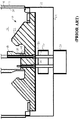
図1を参照すると、従来のX線管12の高電圧絶縁体部分10の拡大断面図が示されている。X線管12は、内部真空部16を備えた真空容器14を有する。陰極ポスト18が真空16内に設けられ、高電圧コネクタ組立体22を介して高電圧ケーブル20から電力を受け取る。コネクタ組立体22は、真空容器14に結合される主コネクタ24とファラデー箱26とを含む。ファラデー箱26は、周囲に電磁シールドを形成し且つコネクタ接続部30の絶縁破壊を防ぐ。
Referring to FIG. 1, an enlarged cross-sectional view of a high voltage insulator portion 10 of a
高電圧絶縁体32は、陰極ポスト18と真空容器14の壁34との間で、コネクタ組立体22の側面に沿って結合される。陰極ポスト18とファラデー箱26は、絶縁体32とコネクタ24とによって隔てられていることに留意されたい。陰極ポスト18と真空部16付近の絶縁体32との間の接続部44には、三重点領域が存在する。ファラデー箱26と絶縁体32との間の領域には、高電界応力領域が存在する。三重点領域は破線円38で示され、高電界応力領域は、破線円40で示され、且つ高電界が不均一な範囲である。領域38及び40は、図2に示される三重点領域38と高電界領域40である。
A
次に、図2を参照すると、絶縁体部分10の静電界線を表す4分の1拡大断面図が示されている。静電界線42は、陰極ポスト18とファラデー箱26に沿って絶縁体32を通ってほぼ延びる等電位線として示される。電界線42は、絶縁体32内の陰極ポスト18の端部44及びファラデー箱26の端部46の近傍で曲っていることに留意されたい。この電界線42の湾曲が、三重点領域38及び高電界応力領域40内の高電界応力の原因となる。電界線42の曲率が急であるほど、電界応力は強くなる。一般的に、電界線の急な湾曲は、金属形状の鋭い角及び不連続部に存在する。電子は、矢印48で示されるように、端部44から絶縁体32の表面をわたり固体から真空中へ放出される。これは電界効果放出と呼ばれる。時間の経過と共に、絶縁体32をわたる電界効果照射により、絶縁体32に亀裂が生じ、最終的にはX線管12が動作不能となる。本発明の多くの実施形態は、陰極ポスト及びファラデー箱の近傍などでX線管内の静電界線の湾曲を防止する。上記の実施形態を以下に詳細に説明する。
Next, referring to FIG. 2, a one-quarter enlarged sectional view showing the electrostatic field lines of the insulator portion 10 is shown. Electrostatic field lines 42 are shown as equipotential lines that extend generally through
以下の図では、同じ参照符号は同じ構成要素を表すように用いられる。本発明は、X線管の三重点領域内の静電界線の湾曲を最小化する装置に関して説明しているが、以下の、コンピュータ断層撮影(CT)システム、放射線治療システム、X線イメージング・システム、及び当該技術分野で公知の他の用途の装置は、種々の目的に適合させることが可能であり、これらの用途に限定されるものではない。本発明は、X線管、CT管、及び当該技術分野で公知の他のイメージング管に適用することができる。本発明は、単極及び双極イメージング管に適用することができる。 In the following figures, the same reference numerals are used to represent the same components. The present invention has been described with respect to an apparatus for minimizing the curvature of electrostatic field lines in the triple point region of an X-ray tube. The following are computed tomography (CT) systems, radiation therapy systems, X-ray imaging systems. And other applications known in the art can be adapted for various purposes and are not limited to these applications. The present invention can be applied to X-ray tubes, CT tubes, and other imaging tubes known in the art. The present invention can be applied to monopolar and bipolar imaging tubes.
以下の説明において、種々の動作パラメータ及び構成要素が、1つの構成された実施形態において説明される。これらの特定のパラメータ及び構成要素は、例証として含まれるものであり、限定を意図するものではない。 In the following description, various operating parameters and components are described in one configured embodiment. These specific parameters and components are included as examples and are not intended to be limiting.
また、用語「三重点領域」は、イメージング管の真空容器内の領域を意味し、これに沿って高電圧接続部と高電圧絶縁体とが互いに隣接し、近接し、又は接触する。三重点領域は、絶縁体の外部又は内部の領域を含むことができる。例示的な三重点領域は図1、2、5及び6に示される。 The term “triple region” means a region in the vacuum vessel of the imaging tube along which the high voltage connection and the high voltage insulator are adjacent to, in close proximity to, or in contact with each other. The triple point region can include a region outside or inside the insulator. Exemplary triple point regions are shown in FIGS.
次に、図3及び図4を参照すると、本発明の実施形態によるイメージング管52を使用したマルチスライスCTイメージング・システム50の斜視図及び概略ブロック図が示される。イメージング・システム50は、X線管組立体56と検出器アレイ58とを有するガントリ54を含む。組立体56は、イメージング管52などのX線発生装置を有する。イメージング管52は、X線ビーム60を検出器アレイ58に向けて投射する。イメージング管52及び検出器アレイ58は、並進移動可能テーブル62の周りを回転する。テーブル62は、組立体56と検出器アレイ58との間でz軸に沿って並進し、ヘリカル・スキャンを実行する。患者ボア66内で患者64を透過した後のビーム60は、検出器アレイ58で検出される。ビーム60を受信すると検出器アレイ58は、CT画像の生成に用いられる投影データを発生する。
3 and 4, a perspective view and schematic block diagram of a multi-slice
イメージング管52及び検出器アレイ58は、中心軸68の周りを回転する。ビーム60は多数の検出器素子70によって受信される。各検出器素子70は、入射X線ビーム60の強度に応じた電気信号を発生する。ビーム60が患者64を透過すると、該ビーム60は減弱される。ガントリ54の回転及び管52の動作は、制御機構71によって制御される。制御機構71は、管52に電力とタイミング信号とを供給するX線制御装置72と、ガントリ54の回転速度及び位置を制御するガントリ・モータ制御装置74とを含む。データ収集システム(DAS)76は、検出器素子70から発生されるアナログ・データをサンプリングし、後続の処理のために該アナログ・データをデジタル信号に変換する。画像再構成装置78は、サンプリングされてデジタル化された、DAS76からのX線データを受け取り、高速画像再構成を実行してCT画像を生成する。主制御装置、すなわちコンピュータ80が、CT画像を大容量記憶装置82内に格納する。
Imaging tube 52 and detector array 58 rotate about a central axis 68. Beam 60 is received by a number of detector elements 70. Each detector element 70 generates an electrical signal corresponding to the intensity of the incident X-ray beam 60. As beam 60 passes through patient 64, beam 60 is attenuated. The rotation of the gantry 54 and the operation of the tube 52 are controlled by the control mechanism 71. The control mechanism 71 includes an
コンピュータ80はまた、オペレータ・コンソール84を介してオペレータから命令及びスキャン・パラメータを受け取る。表示装置86によって、オペレータはコンピュータからの再構成画像及び他のデータを観察することができる。オペレータが供給した命令及びパラメータは、制御機構71の動作においてコンピュータ80によって用いられる。更にコンピュータ80は、テーブル・モータ制御装置88を作動させ、該制御装置がテーブル62を並進させて患者64をガントリ54内で位置決めする。
次に、図5を参照すると、大気側電磁シールド94に導電的に近接し、且つ本発明の実施形態による陰極ポスト92を有するX線管52の高電圧絶縁体部分90の拡大断面図が示される。X線管52は、内部真空部98を備えた真空容器96及び中心軸100を有する。陰極組立体102は、真空部98内に設けられ、高電圧大気側給電線組立体104から電力を受け取る。高電圧絶縁体106は、陰極組立体104、真空容器96の壁108、及び給電線組立体104の間に結合される。陰極ポスト92は、給電線組立体104と接触するように絶縁体106を貫通して延びる。陰極ポスト92が延びることにより、陰極ポスト92とシールド94との間の分離距離が最小になる。陰極ポスト92とシールド94との間の分離距離が最小になることで、これらの間に電気的な伝導が可能となる。
Referring now to FIG. 5, an enlarged cross-sectional view of the high
陰極組立体102は、アウターハウジング110を有する陰極ポスト92を含む。複数の陰極接続部112がアウターハウジング110内に設けられ、給電線組立体104に結合される。
The cathode assembly 102 includes a
給電線組立体104は、真空容器96に結合される主コネクタ114を含む。主コネクタ114は、ファラデー箱の形態とすることができるシールド94を含む。シールド94は、コネクタ114内で、且つ接続点での絶縁体106とコネクタ114との間の境界面でコネクタ接続部116を取り囲み、その絶縁破壊を防止する。コネクタ接続部116は、高電圧ケーブル118から電力を受け取り、陰極接続部112へ電力を供給する。主コネクタ114及びシールド94は、種々の形態、形状、及び寸法とすることができる。
The
絶縁体106は、陰極ポスト内部部分120、陰極ポストチャンネル122、及び外部部分124を有する。内部部分120は、完全に陰極ポスト92内部に設けることができる。陰極ポスト92は、チャンネル122内部に設けられる。絶縁体106は、真空容器96の外部にある大気126から真空部98を絶縁して分離する。絶縁体106はまた、陰極ポスト92、給電線組立体104、及び壁108の間の電位を絶縁し分離する。絶縁体106は、高絶縁耐力を有する厚いセラミック絶縁体などの誘電性絶縁体の形態とすることができ、又は当該技術分野で公知の他の形式とすることができる。絶縁体106はまた、種々の形態、形状、寸法とすることができる。
The
X線管52内の三重点領域及び高電界応力領域は、それぞれ破線円130及び131で示される。三重点領域130内及び高電界応力領域131内の静電界の湾曲は、シールド94に対する陰極ポスト92の導電的近接によって最小化される。これは図6で更に詳細に分かる。
The triple point region and high electric field stress region in the X-ray tube 52 are indicated by dashed
図6を参照すると、本発明の実施形態による図5の絶縁部分90の静電界線を表す4分の1拡大断面図を示す。絶縁体106内で陰極ポスト92に沿った静電界線132の湾曲が最小であることに留意されたい。陰極ポストの端部134及びシールド94の端部136の間及びその近傍で最小量の湾曲が存在する。X線管52内の電磁界応力は、三重点領域130及び高電界応力領域131において、図1に示されるような従来技術のX線管内の電磁界応力よりも実質的に小さい。電界線132が本来の同軸配列により近接して従う結果、電界線132は中心軸100に対してほぼ平行であり、陰極ポスト92及びシールド94などの真空容器96内に含まれる任意の中実の金属面に対して直角に終端するようになる。最小量の湾曲の残部は、図7の実施形態によって更に解消される。
Referring to FIG. 6, a quarter enlarged cross-sectional view representing the electrostatic field lines of the insulating
次に図7を参照すると、本発明の実施形態による、X線管52'の高電圧絶縁体部分90’の拡大断面図が、陰極ポスト92'が大気側電磁シールド94'と導電接触した状態で示されている。図7は本発明の別の実施形態を示す。X線管52'は、陰極組立体102’、絶縁体106'、及び給電線組立体104'を含む。絶縁体106’は、絶縁体106'の中心部分142に設けられる導電素子140を有する。導電素子140は、陰極ポスト92'及び給電線組立体104’に導電接触する。また、シールド94'は、中心軸100に沿ってシールド94よりも更に延長され、導電素子140に接触するようにする。
Referring now to FIG. 7, an enlarged cross-sectional view of the high
導電素子140は、陰極ポスト92’とシールド94'との間に設けられ、電流を伝える。導電素子140は導電リングの形態で示されるが、種々の形態、形状、及び寸法であってもよい。導電素子140は、金属材料又は当該技術分野で公知の他の導電性材料で形成することができる。 The conductive element 140 is provided between the cathode post 92 'and the shield 94' and conducts current. Although the conductive element 140 is shown in the form of a conductive ring, it may be in various forms, shapes, and dimensions. The conductive element 140 can be formed of a metal material or other conductive material known in the art.
図7の実施形態は、陰極ポスト92'とシールド94'との間に連続した導電接続部を形成する。連続した導電接続部は、絶縁体106'の内外の陰極ポスト92'及びシールド94'に沿った静電界線の湾曲を除去する。連続した導電接続部は、更に、図6に示される陰極ポスト92とシールド94との間のギャップ152の排除によりこれらの間の少量の湾曲部150を最小限にする。
The embodiment of FIG. 7 forms a continuous conductive connection between the
本発明は、陰極ポストと高電圧給電線組立体の電磁シールドとの間の最小限のギャップを具備するX線管を提供する。陰極ポストとシールドとの間のギャップを縮小すると、X線管の三重点領域及び高電界応力領域の電界応力が低下する。電界応力の低下は、スピット活動を最小にし、X線管の高電圧安定性を向上させる。本発明は、絶縁体表面に沿った電界加速及びカスケード増強放電開始に起因する電荷移動度を最小限に抑える。本発明はまた、X線管の高電圧絶縁体の絶縁耐力も向上させる。 The present invention provides an x-ray tube with a minimal gap between the cathode post and the electromagnetic shield of the high voltage feeder assembly. When the gap between the cathode post and the shield is reduced, the electric field stress in the triple point region and the high electric field stress region of the X-ray tube decreases. The reduction in field stress minimizes spit activity and improves the high voltage stability of the x-ray tube. The present invention minimizes charge mobility resulting from electric field acceleration along the insulator surface and initiation of cascade enhanced discharge. The present invention also improves the dielectric strength of the high voltage insulator of the X-ray tube.
上述の装置及び方法は、当業者であれば当該技術分野で公知の種々の用途及びシステムに適用することができる。上述の発明はまた、本発明の真の範囲から逸脱することなく変更することができる。 The apparatus and method described above can be applied by those skilled in the art to various uses and systems known in the art. The above-described invention can also be modified without departing from the true scope of the invention.
92 陰極ポスト
94 電磁シールド
96 真空容器
98 内部真空部
104 大気側給電線組立体
106 絶縁体
92
Claims (10)
内部真空部(98)を有する真空容器(96)と、
電磁シールド(94、94’)を有する大気側給電線組立体(104、104’)と、
外部大気(126)から前記内部真空部(98)を分離する絶縁体(106、106’)と、
前記電磁シールド(94、94’)に電気的に接続し、前記電磁シールド(94、94’)に近接し且つイメージング管(52、52’)内の静電界線(132)の湾曲を防ぐ、前記真空容器(96)内に少なくとも部分的に存在する陰極ポスト(92、92’)と、
を備え、
前記陰極ポスト(92、92’)が、
アウターハウジング(110)と、
前記アウターハウジング(110)内に存在する複数の陰極接続部と、
を含むイメージング管(52、52’)。 In the imaging tube (52, 52 ′)
A vacuum vessel (96) having an internal vacuum (98);
An atmosphere side feeder assembly (104, 104 ') having an electromagnetic shield (94, 94');
Insulators (106, 106 ') separating the internal vacuum (98) from the external atmosphere (126);
Electrically connected to the electromagnetic shield (94, 94 ') to prevent bending of the electrostatic field lines (132) proximate to the electromagnetic shield (94, 94') and in the imaging tube (52, 52 '); A cathode post (92, 92 ') at least partially present in the vacuum vessel (96);
Bei to give a,
The cathode post (92, 92 ′)
An outer housing (110);
A plurality of cathode connections present in the outer housing (110);
An imaging tube (52, 52 ').
陰極ポスト内部部分(120)と、
陰極ポスト外部部分(124)と、
を含む請求項1に記載のイメージング管(52、52’)。 The insulator (106, 106 ′)
A cathode post internal portion (120);
A cathode post exterior portion (124);
The imaging tube (52, 52 ') of claim 1, comprising:
The imaging tube (52, 52 ') of claim 1, wherein the atmosphere side feeder assembly (104, 104') includes a Faraday box (26) proximate to the cathode post (92, 92 ').
Applications Claiming Priority (2)
| Application Number | Priority Date | Filing Date | Title |
|---|---|---|---|
| US10/707,269 US6901136B1 (en) | 2003-12-02 | 2003-12-02 | X-ray tube system and apparatus with conductive proximity between cathode and electromagnetic shield |
| US10/707,269 | 2003-12-02 |
Publications (3)
| Publication Number | Publication Date |
|---|---|
| JP2005203354A JP2005203354A (en) | 2005-07-28 |
| JP2005203354A5 JP2005203354A5 (en) | 2008-01-24 |
| JP4768253B2 true JP4768253B2 (en) | 2011-09-07 |
Family
ID=34590837
Family Applications (1)
| Application Number | Title | Priority Date | Filing Date |
|---|---|---|---|
| JP2004348517A Expired - Fee Related JP4768253B2 (en) | 2003-12-02 | 2004-12-01 | X-ray tube system and apparatus having conductive proximity between cathode and electromagnetic shield |
Country Status (3)
| Country | Link |
|---|---|
| US (1) | US6901136B1 (en) |
| JP (1) | JP4768253B2 (en) |
| DE (1) | DE102004058289A1 (en) |
Families Citing this family (10)
| Publication number | Priority date | Publication date | Assignee | Title |
|---|---|---|---|---|
| EP1537594B1 (en) * | 2002-09-09 | 2006-01-25 | Comet Holding AG | High-voltage vacuum tube |
| US7020244B1 (en) * | 2004-12-17 | 2006-03-28 | General Electric Company | Method and design for electrical stress mitigation in high voltage insulators in X-ray tubes |
| US7668295B2 (en) * | 2007-05-14 | 2010-02-23 | General Electric Co. | System and method for high voltage transient suppression and spit protection in an x-ray tube |
| JP5278895B2 (en) * | 2008-04-25 | 2013-09-04 | 株式会社日立メディコ | Anode grounded X-ray tube equipment |
| US7881436B2 (en) | 2008-05-12 | 2011-02-01 | General Electric Company | Method and apparatus of differential pumping in an x-ray tube |
| US7783012B2 (en) * | 2008-09-15 | 2010-08-24 | General Electric Company | Apparatus for a surface graded x-ray tube insulator and method of assembling same |
| US8675818B2 (en) * | 2011-04-12 | 2014-03-18 | Varian Medical Systems, Inc. | Ceramic metallization in an x-ray tube |
| JP2016186880A (en) * | 2015-03-27 | 2016-10-27 | 東芝電子管デバイス株式会社 | X-ray tube |
| US11201031B2 (en) * | 2018-03-22 | 2021-12-14 | Varex Imaging Corporation | High voltage seals and structures having reduced electric fields |
| US10923307B1 (en) * | 2020-04-13 | 2021-02-16 | Hamamatsu Photonics K.K. | Electron beam generator |
Family Cites Families (9)
| Publication number | Priority date | Publication date | Assignee | Title |
|---|---|---|---|---|
| DE3116169A1 (en) * | 1981-04-23 | 1982-11-11 | Philips Patentverwaltung Gmbh, 2000 Hamburg | HIGH VOLTAGE VACUUM TUBES, ESPECIALLY X-RAY TUBES |
| US5136625A (en) * | 1991-10-18 | 1992-08-04 | Varian Associates, Inc. | Metal center x-ray tube |
| EP0590418B1 (en) * | 1992-10-02 | 1996-08-14 | Licentia Patent-Verwaltungs-GmbH | High voltage tube |
| US6236713B1 (en) * | 1998-10-27 | 2001-05-22 | Litton Systems, Inc. | X-ray tube providing variable imaging spot size |
| CN1596140A (en) * | 2001-06-19 | 2005-03-16 | 光电子公司 | Optically driven therapeutic radiation source |
| US6570962B1 (en) * | 2002-01-30 | 2003-05-27 | Koninklijke Philips Electronics N.V. | X-ray tube envelope with integral corona shield |
| US6816574B2 (en) * | 2002-08-06 | 2004-11-09 | Varian Medical Systems, Inc. | X-ray tube high voltage connector |
| US6922463B2 (en) * | 2002-11-14 | 2005-07-26 | Ge Medical Systems Global Technology Company, Llc | Thermally high conductive HV connector for a mono-polar CT tube |
| US6798865B2 (en) * | 2002-11-14 | 2004-09-28 | Ge Medical Systems Global Technology | HV system for a mono-polar CT tube |
-
2003
- 2003-12-02 US US10/707,269 patent/US6901136B1/en not_active Expired - Lifetime
-
2004
- 2004-12-01 JP JP2004348517A patent/JP4768253B2/en not_active Expired - Fee Related
- 2004-12-02 DE DE102004058289A patent/DE102004058289A1/en not_active Withdrawn
Also Published As
| Publication number | Publication date |
|---|---|
| US6901136B1 (en) | 2005-05-31 |
| DE102004058289A1 (en) | 2005-07-28 |
| JP2005203354A (en) | 2005-07-28 |
| US20050117704A1 (en) | 2005-06-02 |
Similar Documents
| Publication | Publication Date | Title |
|---|---|---|
| US6816574B2 (en) | X-ray tube high voltage connector | |
| JP4768253B2 (en) | X-ray tube system and apparatus having conductive proximity between cathode and electromagnetic shield | |
| US7702077B2 (en) | Apparatus for a compact HV insulator for x-ray and vacuum tube and method of assembling same | |
| EP2697814B1 (en) | Metalized ceramic sealing plate for an x-ray tube | |
| US7553080B2 (en) | Grounded rotating anode x-ray tube housing | |
| JPH08280665A (en) | X-ray computer tomography | |
| JP7048396B2 (en) | X-ray tube | |
| JP4876047B2 (en) | X-ray generator and X-ray CT apparatus | |
| US6798865B2 (en) | HV system for a mono-polar CT tube | |
| US8308506B2 (en) | Ultra-low capacitance high voltage cable assemblies for CT systems | |
| JPH0355933B2 (en) | ||
| EP0563367A4 (en) | ||
| KR101864214B1 (en) | Micro x-ray tube | |
| US4053802A (en) | High-voltage vacuum tube, particularly an x-ray tube | |
| US10032595B2 (en) | Robust electrode with septum rod for biased X-ray tube cathode | |
| CN112216584A (en) | X-ray generator with shielding component | |
| CN113272931B (en) | X-ray generating tube, X-ray generating apparatus, and X-ray imaging apparatus | |
| US4757524A (en) | X-ray generator | |
| CN106376166B (en) | High voltage source for x-ray emission device | |
| US7020244B1 (en) | Method and design for electrical stress mitigation in high voltage insulators in X-ray tubes | |
| EP3394876B1 (en) | Target assembly for an x-ray emission apparatus and x-ray emission apparatus | |
| US7197114B2 (en) | X-rays emitter and X-ray apparatus and method of manufacturing an X-ray emitter | |
| CN217444331U (en) | Cold cathode X-ray tube and X-ray generator | |
| GB2094057A (en) | X-ray generator | |
| CN114551192A (en) | Cold cathode X-ray tube and X-ray generator |
Legal Events
| Date | Code | Title | Description |
|---|---|---|---|
| A521 | Written amendment |
Free format text: JAPANESE INTERMEDIATE CODE: A523 Effective date: 20071129 |
|
| A621 | Written request for application examination |
Free format text: JAPANESE INTERMEDIATE CODE: A621 Effective date: 20071129 |
|
| RD02 | Notification of acceptance of power of attorney |
Free format text: JAPANESE INTERMEDIATE CODE: A7422 Effective date: 20101124 |
|
| RD04 | Notification of resignation of power of attorney |
Free format text: JAPANESE INTERMEDIATE CODE: A7424 Effective date: 20101124 |
|
| A977 | Report on retrieval |
Free format text: JAPANESE INTERMEDIATE CODE: A971007 Effective date: 20101203 |
|
| A131 | Notification of reasons for refusal |
Free format text: JAPANESE INTERMEDIATE CODE: A131 Effective date: 20101214 |
|
| A521 | Written amendment |
Free format text: JAPANESE INTERMEDIATE CODE: A523 Effective date: 20110302 |
|
| A01 | Written decision to grant a patent or to grant a registration (utility model) |
Free format text: JAPANESE INTERMEDIATE CODE: A01 Effective date: 20110531 |
|
| A01 | Written decision to grant a patent or to grant a registration (utility model) |
Free format text: JAPANESE INTERMEDIATE CODE: A01 |
|
| A61 | First payment of annual fees (during grant procedure) |
Free format text: JAPANESE INTERMEDIATE CODE: A61 Effective date: 20110616 |
|
| R150 | Certificate of patent or registration of utility model |
Free format text: JAPANESE INTERMEDIATE CODE: R150 |
|
| FPAY | Renewal fee payment (event date is renewal date of database) |
Free format text: PAYMENT UNTIL: 20140624 Year of fee payment: 3 |
|
| LAPS | Cancellation because of no payment of annual fees |