JP4763581B2 - Optical pickup device - Google Patents
Optical pickup device Download PDFInfo
- Publication number
- JP4763581B2 JP4763581B2 JP2006319080A JP2006319080A JP4763581B2 JP 4763581 B2 JP4763581 B2 JP 4763581B2 JP 2006319080 A JP2006319080 A JP 2006319080A JP 2006319080 A JP2006319080 A JP 2006319080A JP 4763581 B2 JP4763581 B2 JP 4763581B2
- Authority
- JP
- Japan
- Prior art keywords
- light
- optical system
- sub
- reflected
- signal
- Prior art date
- Legal status (The legal status is an assumption and is not a legal conclusion. Google has not performed a legal analysis and makes no representation as to the accuracy of the status listed.)
- Expired - Fee Related
Links
Images


Classifications
-
- G—PHYSICS
- G11—INFORMATION STORAGE
- G11B—INFORMATION STORAGE BASED ON RELATIVE MOVEMENT BETWEEN RECORD CARRIER AND TRANSDUCER
- G11B7/00—Recording or reproducing by optical means, e.g. recording using a thermal beam of optical radiation by modifying optical properties or the physical structure, reproducing using an optical beam at lower power by sensing optical properties; Record carriers therefor
- G11B7/12—Heads, e.g. forming of the optical beam spot or modulation of the optical beam
- G11B7/135—Means for guiding the beam from the source to the record carrier or from the record carrier to the detector
- G11B7/1372—Lenses
- G11B7/1378—Separate aberration correction lenses; Cylindrical lenses to generate astigmatism; Beam expanders
-
- G—PHYSICS
- G11—INFORMATION STORAGE
- G11B—INFORMATION STORAGE BASED ON RELATIVE MOVEMENT BETWEEN RECORD CARRIER AND TRANSDUCER
- G11B7/00—Recording or reproducing by optical means, e.g. recording using a thermal beam of optical radiation by modifying optical properties or the physical structure, reproducing using an optical beam at lower power by sensing optical properties; Record carriers therefor
- G11B7/08—Disposition or mounting of heads or light sources relatively to record carriers
- G11B7/09—Disposition or mounting of heads or light sources relatively to record carriers with provision for moving the light beam or focus plane for the purpose of maintaining alignment of the light beam relative to the record carrier during transducing operation, e.g. to compensate for surface irregularities of the latter or for track following
- G11B7/0901—Disposition or mounting of heads or light sources relatively to record carriers with provision for moving the light beam or focus plane for the purpose of maintaining alignment of the light beam relative to the record carrier during transducing operation, e.g. to compensate for surface irregularities of the latter or for track following for track following only
- G11B7/0903—Multi-beam tracking systems
-
- G—PHYSICS
- G11—INFORMATION STORAGE
- G11B—INFORMATION STORAGE BASED ON RELATIVE MOVEMENT BETWEEN RECORD CARRIER AND TRANSDUCER
- G11B7/00—Recording or reproducing by optical means, e.g. recording using a thermal beam of optical radiation by modifying optical properties or the physical structure, reproducing using an optical beam at lower power by sensing optical properties; Record carriers therefor
- G11B7/12—Heads, e.g. forming of the optical beam spot or modulation of the optical beam
- G11B7/135—Means for guiding the beam from the source to the record carrier or from the record carrier to the detector
- G11B7/1362—Mirrors
-
- G—PHYSICS
- G11—INFORMATION STORAGE
- G11B—INFORMATION STORAGE BASED ON RELATIVE MOVEMENT BETWEEN RECORD CARRIER AND TRANSDUCER
- G11B7/00—Recording or reproducing by optical means, e.g. recording using a thermal beam of optical radiation by modifying optical properties or the physical structure, reproducing using an optical beam at lower power by sensing optical properties; Record carriers therefor
- G11B2007/0003—Recording, reproducing or erasing systems characterised by the structure or type of the carrier
- G11B2007/0009—Recording, reproducing or erasing systems characterised by the structure or type of the carrier for carriers having data stored in three dimensions, e.g. volume storage
- G11B2007/0013—Recording, reproducing or erasing systems characterised by the structure or type of the carrier for carriers having data stored in three dimensions, e.g. volume storage for carriers having multiple discrete layers
Description
本発明は光ピックアップ装置に関し、特に光ピックアップ装置の読出し光学系に関する。 The present invention relates to an optical pickup device, and more particularly to a readout optical system of the optical pickup device.
光ディスクの1層の容量は使用する半導体レーザの波長と対物レンズの開口数(NA)に大きく依存する。半導体レーザの波長が短いほど、あるいはNAが大きいほど、記録密度を大きくでき、1層あたりの容量を増やすことができる。現在市場に流通している光ディスクドライブの主体は波長650nm付近の赤色光とNA0.6の対物レンズを使用するDVD(Digital Versatile Disk)ドライブであるが、DVDの記録密度を上回るものとして、光波長405nm付近の青紫色の半導体レーザを光源とし、NA0.85の対物レンズを使用する光ディスクドライブが出荷され始めている。今後の記録密度向上のために使用波長の短波長化を考えたとき、この青紫色より短い波長の半導体レーザ光源の開発は波長が紫外域になるため、開発に困難が予想される。また、空気中での対物レンズのNAの限界は1であるので、対物レンズによる記録密度の向上も困難になってきている。 The capacity of one layer of the optical disk greatly depends on the wavelength of the semiconductor laser used and the numerical aperture (NA) of the objective lens. As the wavelength of the semiconductor laser is shorter or as the NA is larger, the recording density can be increased and the capacity per layer can be increased. The main optical disk drive currently on the market is a DVD (Digital Versatile Disk) drive that uses red light with a wavelength of around 650 nm and an objective lens with NA of 0.6. Optical disk drives using a blue-violet semiconductor laser near 405 nm as a light source and using an objective lens with NA of 0.85 are beginning to be shipped. Considering shortening the wavelength used to improve the recording density in the future, the development of a semiconductor laser light source with a wavelength shorter than blue-violet is expected to be difficult to develop because the wavelength is in the ultraviolet region. Further, since the NA limit of the objective lens in air is 1, it is difficult to improve the recording density with the objective lens.
このような状況において、1枚の光ディスクの容量を増加させる方式として多層化が提案されている。非特許文献1には4層のROM(Read Only Memory)が紹介されている。レーザ光を多層光ディスクに照射した場合、同時に複数の層を照射することになるので層間のクロストークが問題となる。この問題を低減するために、層間隔を大きくすることが行われる。レーザ光は集光されており、目的とする層以外はレーザ光の集光位置からずれるので、クロストークを低減することができる。
Under such circumstances, multilayering has been proposed as a method for increasing the capacity of one optical disk. Non-Patent
一方、層間隔を広げると球面収差が問題になってくる。記録層の層間には空気の屈折率と異なるポリカーボネイトが使用されており、球面収差の原因となる。対物レンズの球面収差は特定の層に対して小さくなるように設計されており、他の層にレーザ光の焦点を移したとき球面収差が発生する。この収差は、通常2枚のレンズで構成されるエクスパンダーレンズ光学系あるいは液晶素子を対物レンズの前に置くことで補正することが可能である。2枚のレンズの距離あるいは液晶素子の位相を変えることで収差を補正することができる。しかし、液晶素子の補償可能範囲あるいはレンズの移動機構を小型の光ディスクドライブ装置内で実現することを考慮すると、大きい球面収差を補正することはできない。すなわち、多層光ディスクの層間隔を十分広くとることは実際の光ドライブ装置では事実上難しくなる。この結果、多層光ディスクでは層間クロストークが残ることになる。 On the other hand, when the layer spacing is increased, spherical aberration becomes a problem. Polycarbonates different from the refractive index of air are used between the recording layers, which causes spherical aberration. The spherical aberration of the objective lens is designed to be small with respect to a specific layer, and spherical aberration occurs when the focus of the laser beam is moved to another layer. This aberration can be corrected by placing an expander lens optical system or liquid crystal element, which is normally composed of two lenses, in front of the objective lens. The aberration can be corrected by changing the distance between the two lenses or the phase of the liquid crystal element. However, considering that the liquid crystal element can be compensated or the lens moving mechanism is realized in a small optical disk drive, large spherical aberration cannot be corrected. That is, it is practically difficult for the actual optical drive device to have a sufficiently large layer interval of the multilayer optical disk. As a result, interlayer crosstalk remains in the multilayer optical disc.
前述のクロストークを低減するために、特許文献1によれば、レンズで集光された多層光ディスクからの反射光の集光位置は目的とする層と隣接層では光軸上で異なるので、微小なミラーを光軸上に配置することで、目的とする反射光だけを取り出すことができ、クロストークの低減が可能となる。しかし、光ディスクからの反射光を光軸に対して横方向に曲げる方式であるため、光ヘッドは大きくならざるを得ない。また、特許文献2によれば、臨界角プリズムを使用して、隣接層からの反射光を取り除く方法が提案されている。この方法では、当該層からの反射光はコリメートされた平行光になるが、隣接層からの反射光は発散光あるいは収束光になることを利用し、光軸に対してある角度以上になった光線を、臨界角プリズムで除去しようとするものである。この方式も、臨界プリズムを2個使用するので、光ヘッドが大きくならざるを得ない。
In order to reduce the above-described crosstalk, according to
図3を用いて、光ピックアップ装置の検出光学系における多層光ディスクによるクロストークを説明する。トラッキングエラー信号の検出はここではDPP(Differential Push-Pull)法を使用するものとする。DPP法では回折格子によりレーザ光を1本の主光線と2本の副光線に分割して光ディスクを照射する。図3では主光線80のみを示している。単純化のために、501は2層の光ディスクとし、511および512は情報記録層である。対物レンズ401からの主光線の最小ビームスポット位置は主光線80で示すように情報記録層511上にあり、情報記録層511からの情報を読み出そうとしている。情報記録層511上には、図4に示すトラッキングのための案内溝が形成されており、この溝を主光線が光スポット94として照射し、同時に副光線は半トラックピッチだけずれた位置を照射スポット95、96として照射している。照射光の焦点は記録層511に合っているので、その反射光は入射光と同じ光路を逆方向に辿って図3の対物レンズ401に戻る。次に、検出レンズ402を透過し、光ビーム81となって光検出器51に入射する。検出レンズ402には非点収差が入っており、光検出器51は最小錯乱円の位置に設置される。
With reference to FIG. 3, the crosstalk caused by the multilayer optical disk in the detection optical system of the optical pickup device will be described. The tracking error signal is detected here using a DPP (Differential Push-Pull) method. In the DPP method, a laser beam is divided into one principal ray and two sub rays by a diffraction grating to irradiate the optical disc. In FIG. 3, only the
光検出器の形状とディスクからの反射光の入射状態を図5に示す。中央にある田の字状の4分割された検出器541は主光線を検出するものであり、主光線は811のスポットとして検出器541を照射する。副光線による反射光は、それぞれ2分割検出器542、543上に光スポット812、813として入射する。4分割検出器541からの信号をA、B、C、Dとし、2分割検出器542からの信号をE、Fおよび2分割検出器543からの信号をG、Hとする。このとき、トラッキングエラー信号TRは、TR=(A+B)−(C+D)−k{(E−F)+(G−H)}と表される。ここに、kは定数であり、主光線と副光線の強度比等から決められる。通常、主光線は副光線の強度と比較して10倍以上大きくなるように設定されている。また、フォーカスエラー信号をAF、データ信号をRFとしたとき、AF=A+C−(B+D)、RF=A+C+B+Dのように表される。TRおよびAF信号はレーザ光の照射位置の制御に使用される。
FIG. 5 shows the shape of the photodetector and the incident state of reflected light from the disk. A quadrant-shaped detector 541 at the center detects a chief ray, and the chief ray irradiates the detector 541 as an 811 spot. The reflected light by the sub-rays enters the two-
多層ディスクにレーザ光を照射したとき、それぞれの層からの反射光量はほぼ同量になるように設計されている。このために対物レンズに近い層の透過率が大きくなっており、対物レンズから遠い層にもレーザ光が照射できるようになっている。このような条件下では、図3に示したように情報読出し対象層である511にレーザ光の焦点を合わせると、一部のレーザ光は光ビーム82として当該層511を透過し、隣接層512で反射され、迷光である反射光ビーム83となる。この反射光ビーム83は対物レンズ401に戻り、検出レンズ402に入射した後、光検出器51の手前で一旦集光され、光ビーム84で示したように広がりながら光検出器51に入射する。光ビーム84は、光検出器面上では図5に示すように、広がった光スポット841になり、光検出器541、542、543を覆った状態となる。このため、ビーム811および812、813と干渉することになる。この干渉は、層間隔の変動による光スポット841の位相の変化に影響され、変動する。すなわち、これによる干渉状態の変動のために、ビーム811の全光量であるRF信号強度における変動はRF信号のジッターの劣化を引き起こし、データ読み出し時のエラーレートを悪化させてしまう。また、回折格子で分割されて生成される副光線の強度は設計上小さく設定されているので、隣接層からの主光線の反射光のパワーデンシティと同程度となり、このため、干渉の効果が強く現れる。この干渉も光ディスクの傾きや層間隔などに影響され、不均一な層間隔のディスクの回転で光スポット812あるいは813の光量分布が変化する。この結果、TR信号の差動信号部分(E−F)+(G−H)に影響を与えることになり、トラッキング信号のバランスを崩すことになる。これにより、トラッキングがはずれるような不具合が生じる。同様に、隣接層512が読出し対象層511の対物レンズ寄りにある場合も、隣接層から反射光が発生し、問題となる干渉が同様に生じる。
When the multilayer disk is irradiated with laser light, the amount of reflected light from each layer is designed to be substantially the same. For this reason, the transmittance of the layer close to the objective lens is increased, and the layer far from the objective lens can be irradiated with laser light. Under such conditions, when the laser beam is focused on the information
本発明の目的は、光ピックアップ装置を大型化させずに、多層光ディスクでのデータ信号やトラッキング信号へのクロストークを軽減することである。 An object of the present invention is to reduce crosstalk to a data signal and a tracking signal in a multilayer optical disk without increasing the size of the optical pickup device.
上述の課題を解決するために、主光線の隣接層からの反射の影響を少なくする方法を用いる。図3の光学系では集光レンズ402に非点収差が導入されており、光検出器は収束ビームが最小錯乱円となる光軸位置に置かれる。この場合、最小錯乱円は収差のない集光スポットと比較して大きいため、最小錯乱円の位置に置いた光検出器は広くならざるを得ない。この場合、図5において説明したように、隣接層からの反射光841が検出器542、543に迷光として入射してしまう。この迷光を低減するため、隣接光からの迷光を含めた光ディスクからの反射光を一旦非点収差がない、すなわち収差の少ない集光レンズで集光し、集光位置に部分的に反射する領域を設けた反射板を設置する。収差の小さいレンズで集光するので、焦点位置でのスポットサイズは小さくなる。他方、隣接層からの反射光は、非点収差の有無にかかわらず、広がったものなのでパワーデンシティの分布はそれほど変わらない。
In order to solve the above-described problem, a method of reducing the influence of the reflection of the chief ray from the adjacent layer is used. In the optical system of FIG. 3, astigmatism is introduced into the
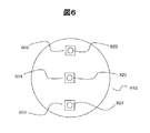
図6に、収差のないレンズで光ディスクからの反射光を絞り込んだ状態を示す。821は当該層からの主光線の反射光の集光スポット、822、823は副光線の反射光の集光スポットである。レンズに収差を入れていないので、図5で示した最小錯乱円よりも、小さいスポットになる。隣接層からの反射光842は大きく広がった状態であり、図5の場合とほとんど変わらない。ここで、部分的な反射領域を有する反射鏡を焦点位置に設置する。図6において、601は四角の形状をした反射部分を表し、主光線を反射する。602、603は同様に反射部分を表し、それぞれ副光線を反射する。この反射部分の大きさは、それぞれの光線のスポット径が小さいので、最小錯乱円の位置に置いた光検出器542あるいは543(図5)より小さくすることができる。図6の反射部分で反射された光を、図5で示した光検出器を用いて検出するとした場合、それぞれの検出器に入射する隣接層からの反射光は、反射部分601〜603の面積が小さいため減少する。一方、821、822、823の当該層からの反射光は大きくは減少しないので、両者が検出器上で干渉したとき、その干渉効果は減少する。
FIG. 6 shows a state in which the reflected light from the optical disk is narrowed by a lens without aberration. 821 is a condensing spot of the reflected light of the principal ray from the layer, and 822 and 823 are condensing spots of the reflected light of the sub-ray. Since the lens has no aberration, the spot becomes smaller than the minimum circle of confusion shown in FIG. The reflected light 842 from the adjacent layer is in a widely spread state, which is almost the same as in the case of FIG. Here, a reflecting mirror having a partial reflection region is installed at the focal position. In FIG. 6,
本発明においては、当該層および隣接層からの反射光を部分的な反射領域を有する反射鏡で反射させてから検出することで、隣接層からの反射光の影響を減少させることができる。同様の効果はピンホールの使用でも得ることが可能であるが、ピンホールは透過タイプであるため、ピンホールの後方に光学系が必要となり、装置が大型化することになる。本発明では部分的な反射領域を有する反射板を用いているので、既設の光学素子を共用できるので、装置の小型化を図ることが可能である。 In the present invention, the influence of the reflected light from the adjacent layer can be reduced by detecting the reflected light from the layer and the adjacent layer after being reflected by the reflecting mirror having a partial reflection region. A similar effect can be obtained by using a pinhole. However, since the pinhole is a transmission type, an optical system is required behind the pinhole, and the apparatus becomes large. In the present invention, since a reflector having a partial reflection region is used, an existing optical element can be shared, so that the size of the apparatus can be reduced.
本発明によると、トラッキングエラー信号を得るための光検出器に入射する隣接層による反射光の光量を減少させることができ、干渉によるトラッキングエラー信号の変動を小さくすることができる。これにより、光ディスクを読み書きするとき、光スポットがトラックをはずれることがなくなる。同時に、光検出器への隣接層からの反射光の影響を少なくすることができるので、データ信号のジッターを小さくすることができ、読み出したデータの信頼性が向上する。 According to the present invention, the amount of reflected light from the adjacent layer incident on the photodetector for obtaining the tracking error signal can be reduced, and the fluctuation of the tracking error signal due to interference can be reduced. As a result, when reading / writing from / to the optical disk, the light spot does not deviate from the track. At the same time, the influence of the reflected light from the adjacent layer on the photodetector can be reduced, so that the jitter of the data signal can be reduced and the reliability of the read data is improved.
以下、本発明の光ディスクドライブ装置を実施するための最良の形態を、図を用いて説明する。 The best mode for carrying out the optical disk drive of the present invention will be described below with reference to the drawings.
図1に、光ディスクドライブ装置の光ピックアップ部分を示す。半導体レーザ101から出射したレーザ光を、コリメータレンズ403と三角プリズム102により円形のコリメートされた光ビームに変換する。コリメートされたビームは回折格子103により3本のビームに分割され、1本の主光線と2本の副光線になる。主光線の進行方向は入射ビームと同じ方向であるが、副ビームは光軸の両側にある傾きを持った出射光となる。通常、主光線と副光線の光量差は10倍以上に設定される。3本のビームは偏光ビームスプリッタ104を透過し、λ/4板105により円偏光に変換され、回転機構により回転する多層ディスク501に対物レンズ404で絞り込まれる。ここでは2層ディスクを図示しているが、2層に限定されるものではなく、3層以上の多層ディスクにも実施可能である。読出し対象層(当該層)は511であり、レーザ光の最小スポットの位置が511上にある。隣接層512からも反射光83が発生し、クロストークの原因である迷光となる。
FIG. 1 shows an optical pickup portion of the optical disk drive device. Laser light emitted from the
多層ディスクからの反射光は迷光も含めて、対物レンズ404を戻り、λ/4板105により、元の偏光方向に対して直交する方向の直線偏光に変換される。このため偏光ビームスプリッタ104で反射され、λ/4板106に向かい、円偏光に変換される。その後、集光レンズ405で集光され、反射板43で反射される。反射板43は記録層511からの反射光が最小スポットになる位置に設置されている。反射板43の形状を図7に示す。主光線は反射領域431で反射され、二つの副光線は反射領域432および433で反射される。それぞれの反射領域の大きさは半径10μmであり、中心間隔は130μmである。反射板43による反射光は集光レンズ405に戻り、λ/4板106により入射時の偏光方向に対して直交した偏光方向の直線偏光となり、ビームスプリッタ104を透過する。406は非点収差が入った集光レンズであり、最小錯乱円の位置に光検出器52が置かれる。光検出器の感度のある部分の形状は図5で示した通りである。光検出器からの信号は信号処理回路53で処理され、光スポットの位置を制御するAF信号およびTR信号、データ信号であるRF信号が形成される。
Reflected light from the multilayer disk, including stray light, returns to the
図10に信号処理のための電子回路を示す。光検出器541および542、543は図5で示したものと同様である。4分割検出器541は主光線を検出し、2分割検出器542、543はそれぞれ副光線を検出する。551から555までが差動増幅器であり、561から566までが加算回路である。580はk倍の増幅器であり、kは主光線と副光線の強度比を勘案して決まる値である。各検出器からの信号はプリアンプで増幅された後、これらの電子回路で処理され、制御信号あるいはデータ信号となる。4分割検出器からの出力AおよびB、C、Dをすべてを加え合わせた信号は572であり、データ信号である。574は非点収差法によるAF信号となる。573は主光線によるプッシュプル信号であり、571は副ビームによる副プッシュプル信号である。571の信号は増幅器580でk倍に増幅され、主光線によるプッシュプル信号573と共に差動増幅器555で処理され、TR信号575となる。
FIG. 10 shows an electronic circuit for signal processing. The
図10の571の副プッシュプル信号(SPP)の計算例を図11に示す。使用波長は0.405μm、対物レンズのNAは0.85、トラックピッチは0.32μmとする。計算では、主光線のスポット位置は対物レンズに近い511の記録層のオントラック上にあり、副光線の位置は半トラックずれた位置に固定されているものとして、層間隔を変化させながら、2層の干渉を考慮したSPPを計算する。このSPPはトラック位置を変化させていないので、干渉効果によるSPPの変動が計算できる。図11の横軸は二つの記録層の層間隔であり、縦軸はSPP振幅で規格化したSPP信号である。白抜きの四角で示した線が実施例1によるSPP信号である。比較のために、反射板43がない通常の光学系、すなわち反射板43の位置に光検出器を541と542、543を配置した光学系での計算結果を同時に示す。この図より、この層間隔の範囲では、SPP信号の変動は、実施例1では0.024であるが、対策のない従来の光学系では0.22となる。
FIG. 11 shows a calculation example of the sub push-pull signal (SPP) 571 in FIG. The wavelength used is 0.405 μm, the NA of the objective lens is 0.85, and the track pitch is 0.32 μm. In the calculation, it is assumed that the spot position of the principal ray is on the on-track of the
本実施例では、集光レンズ405と非点収差入りレンズ406の焦点距離を両者とも46mmとした。集光レンズ405によるスポットサイズは4μmとなる。また,非点収差入りレンズ406の非点隔差は1.7mmであり,最小錯乱円でのスポットサイズは約30μmである。このように小さいスポットサイズのビームを小さい反射領域で反射することができるので,SPP変動を減少させることが可能になる。
In this embodiment, the focal lengths of the
以上のように、本発明によると、層間隔の変動に伴ってトラッキングエラー信号が変動する現象を小さくすることができる。隣接層からの反射光とトラッキングのための副光線が干渉し、その位相差が層間隔で変わるので、サブプッシュプル信号が変動するが、本発明により隣接層からの反射光の影響を小さくできるので、トラッキングエラー信号の変動が小さくなる。これにより、精度の高いレーザ光照射位置の制御が可能となり、読出しおよび書込みのときのレーザ照射位置を正確に決められるので信号の品質が向上する。また、データ信号自体も隣接層からの反射光の混入が小さくなるので、エラーの少ないデータ信号を得ることができる。 As described above, according to the present invention, it is possible to reduce the phenomenon that the tracking error signal fluctuates as the layer spacing fluctuates. The reflected light from the adjacent layer interferes with the tracking sub-beam and the phase difference changes with the layer spacing, so the sub push-pull signal fluctuates, but the present invention can reduce the influence of the reflected light from the adjacent layer. Therefore, the fluctuation of the tracking error signal is reduced. Thereby, it is possible to control the laser beam irradiation position with high accuracy, and the laser irradiation position at the time of reading and writing can be accurately determined, so that the signal quality is improved. In addition, since the data signal itself is less mixed with the reflected light from the adjacent layer, a data signal with few errors can be obtained.
本実施例では偏光光学系を用いたが、半導体レーザの最大出力に十分余裕がある場合は、104の偏光ビームスプリッタを通常のビームスプリッタに置き換え、105と106のλ/4板を取り除いた光学系を使用することも可能である。
In this embodiment, the polarization optical system is used. However, if there is a sufficient margin in the maximum output of the semiconductor laser, the
実施例1では反射板43の形状として、主光線用と副光線用の反射領域の大きさが同じものを使用した。しかし,フォーカスの引き込み範囲が必ずしも設計どおりでない場合がある。これに対処するため、実施例2では、主光線を反射する領域の大きさと副光線を反射する領域の大きさとが異なっている。図1の反射板43の位置に、一例として代替設置すべき反射板を図8に示す。反射板46の反射部分461が主光線用であり、反射部分462、463が副光線用である。この反射板を使用したときの、図10の571の副プッシュプル信号(SPP)の計算例を図12に示す。ここに、462および463の反射領域の半径を10μmとし、461の半径を30μmと40μmに設定した。その他のパラメータは、実施例1と同様に、反射部分の中心間隔を130μmとし、使用波長は0.405μm、対物レンズのNAは0.85、トラックピッチは0.32μmとする。図12の横軸は二つの記録層の層間隔であり、縦軸はSPP振幅で規格化したSPP信号である。△印は中心の反射部分の半径が40μm、○印は半径が30μmのSPP信号を示す。この図より半径が40μmのSPP変動は0.061、半径が30μmの場合のSPP変動は0.053となる。図11で示したように、対策がない場合のSPP変動は0.21なのでSPP変動は減少しており、本発明の効果を示している。
In Example 1, as the shape of the
図13に、光軸方向に光ディスクを移動させたときのAF信号574の変化を示す。横軸はデフォーカス量を表し、デフォーカスがゼロで光ディスクの記録面とレーザ光の最小スポットの位置とが一致している。461の反射部分の半径が30μmのときは引き込み範囲が1.25μm、半径40μmのときは1.45μmとなり、半径を大きくすると引き込み範囲が広くなる。
FIG. 13 shows changes in the AF signal 574 when the optical disk is moved in the optical axis direction. The horizontal axis represents the defocus amount, and the defocus is zero, and the recording surface of the optical disc and the position of the minimum spot of the laser beam coincide with each other. When the radius of the
また、図9に示したストライプ状の反射領域を有する反射板を図1の反射板43の位置に使用しても、隣接層からの反射光の影響を低減することができる。471の反射領域は主光線を反射し、472と473の領域は副光線を反射する。主光線と二つの副光線の中心を通る直線に対して、ストライプの方向は垂直だけでなく、斜めの方向に設定することも可能である。これらの場合、ストライプ状の反射領域を有する反射板は横方向に移動させるだけで、3本のビームと位置調整ができるので、調整が容易になる利点がある。
Further, even if the reflecting plate having the stripe-shaped reflecting region shown in FIG. 9 is used at the position of the reflecting
図2に示した実施例3では、回折格子103と偏光ビームスプリッタ104がコリメータレンズ407より半導体レーザ101側に設置されている。従って、半導体レーザ101から出射したレーザ光は発散光の状態で偏光ビームスプリッタ104を透過し、その後コリメータレンズ407でコリメートされた光ビームに変換されて回折格子105に入射する。実施例1では回折格子103と偏光ビームスプリッタ104がコリメータレンズ403と対物レンズ404の間に設置されていたため、集光レンズ405が必要であったが、実施例3では図2に示すように、多層ディスク501の読出し対象層511から反射された光ビームはコリメータレンズ407を通ると収束光になるため、集光レンズが必要ないので、部品点数を削減できる効果がある。
In the third embodiment illustrated in FIG. 2, the
実施例4を図14に示す。光ディスク501からの反射光は偏光ビームスプリッタ104で反射された後、λ/4板106を透過し円偏光となり、反射板43で反射される。反射板43には光検出器52が、光軸からはずれたところに設置されているが、偏光ビームスプリッタ104で反射された光ディスクからの反射光を直接検出するためのものではない。部分的な反射領域を有する反射板43で反射された光はλ/4板を通過することで、偏光方向が入射時とは90度異なるものとなっているので、偏光ビームスプリッタ104を透過し、凹面鏡48で反射される。凹面鏡の光軸は光検出器52の方向に向いており、反射光は光検出器52で検出される。AF信号を得るために非点収差法を用いるので、凹面鏡48には非点収差が入っている。光検出器52で検出された光による信号は信号処理回路53で処理され、光スポットの位置を制御するAF信号およびTR信号、データ信号であるRF信号が形成される。本実施例では凹面鏡48を用いることで、光検出器への光路を反射板43への光路と共用でき、反射板43上に光検出器を置くことができる。これにより、偏光ビームスプリッタ104より上部の光学系がなくなるので、装置を小型化する効果がある。
Example 4 is shown in FIG. The reflected light from the
SPPの変動を減少させることが可能な光ディスクドライブ装置の実施例を図15に示す。711から714までの回路はデータを多層光ディスク501に記録するためのものである。711は誤り訂正用符号化回路であり、データに誤り訂正符号が付加される。712は記録符号化回路であり、1−7PP方式でデータを変調する。713は記録補償回路であり、マーク長に適した書込みのためのパルスを発生する。発生したパルス列に基づき、半導体レーザ駆動回路714により、光ピックアップ60内の半導体レーザを駆動し、対物レンズから出射したレーザ光80を変調する。モータ502によって回転駆動される光ディスク501上には相変化膜が形成されており、レーザ光で熱せられ、急冷されるとアモルファス状態になり、徐冷されると結晶状態になる。これらの二つの状態は反射率が異なり、マークを形成することができる。書き込み状態では、レーザ光のコヒーレンシーを低下させる高周波重畳を行わないため、隣接層からの反射光と当該層からの反射光は干渉しやすい状態になっている。このため、SPPの変動を低減するための対策を行わない場合は、トラッキングがはずれたり、隣接トラックのデータを消したりする不具合が生じる。本実施例では、光ピックアップ60には実施例1から4で示された光ピックアップのいずれかが採用されており、多層ディスクにおいてもトラッキングの不具合は生じない。
FIG. 15 shows an embodiment of an optical disk drive device capable of reducing the fluctuation of SPP.
721から726の回路はデータの読み出しのためのものである。721はイコライザーであり、最短マーク長付近の信号雑音比を改善する。この信号は722のPLL回路に入力され、クロックが抽出される。また、イコライザーで処理されたデータ信号は抽出されたクロックのタイミングで723のA−D変換器でデジタル化される。724はPRML(Pertial Response Maximum Likelyhood)信号処理回路であり、ビタビ復号を行う。記録復号化回路725では1−7PP方式の変調規則に基づき復号化し、誤り訂正回路726でデータを復元する。
本発明により、光ディスクドライブ装置において多層光ディスクを読み出すときに発生する隣接層からの反射光の影響を低減することができる。多層光ディスクを読み出すときあるいは書き込むとき、光ディスクに対してレーザ光のトラッキング位置の制御を誤差信号により正確に行う必要がある。隣接層からの反射光があると、干渉効果による誤差信号の変移のためにトラッキング位置に狂いが生じ、データ信号を精度よく読み出したり、あるいは書き込み位置を精度よく定めることができなくなる。本発明では、これらの不具合をなくすることができる。さらに、データ信号自体に混入する隣接層からの反射光によるクロストークを低減できるので、データ信号の品質を向上することができる。 According to the present invention, it is possible to reduce the influence of reflected light from an adjacent layer that is generated when a multilayer optical disc is read out in an optical disc drive apparatus. When reading or writing a multilayer optical disc, it is necessary to accurately control the tracking position of the laser beam with respect to the optical disc using an error signal. When there is reflected light from the adjacent layer, the tracking position is deviated due to the shift of the error signal due to the interference effect, and the data signal cannot be read accurately or the writing position cannot be determined accurately. In the present invention, these problems can be eliminated. Furthermore, since the crosstalk due to the reflected light from the adjacent layer mixed in the data signal itself can be reduced, the quality of the data signal can be improved.
43:反射板、46:反射板、47:反射板、48:非点収差入り凹面鏡、52:検出器、53:信号処理回路、101:半導体レーザ、103:回折格子、104:偏光ビームスプリッタ、105:λ/4板、106:λ/4板、404:対物レンズ、405:集光レンズ、406:非点収差入り集光レンズ、501:多層ディスク、541:4分割検出器、542:2分割検出器、543:2分割検出器、601:部分的反射領域、602:部分的反射領域、603:部分的反射領域、821:主光線ビームスポット、822:副光線ビームスポット、823:副光線ビームスポット 43: reflector, 46: reflector, 47: reflector, 48: concave mirror with astigmatism, 52: detector, 53: signal processing circuit, 101: semiconductor laser, 103: diffraction grating, 104: polarization beam splitter, 105: λ / 4 plate, 106: λ / 4 plate, 404: objective lens, 405: condenser lens, 406: condenser lens with astigmatism, 501: multilayer disc, 541: 4-segment detector, 542: 2 Split detector, 543: Two split detector, 601: Partial reflection area, 602: Partial reflection area, 603: Partial reflection area, 821: Main beam spot, 822: Sub beam spot, 823: Sub beam Beam spot
Claims (2)
前記レーザ光源からのレーザ光を主光線と副光線に分割し、前記主光線と副光線を多層光情報記憶媒体の一つの記録層に集光する集光光学系と、
前記多層光情報記憶媒体の前記記録層から反射された反射光を検出する検出光学系とを有し、
前記検出光学系は、前記記録層からの反射光を絞り込む光学系と、前記光学系によって絞り込まれた前記主光線のスポット位置及び前記副光線のスポット位置にそれぞれ独立してストライプ状の反射領域が設けられた反射板と、非点収差入り集光素子と、前記主光線を検出する検出素子及び前記副光線を検出する検出素子を備える光検出器とを含み、前記反射板によって反射された反射光を前記非点収差入り集光素子によって前記光検出器上に集光して検出することを特徴とする光ピックアップ装置。 A laser light source;
A condensing optical system that divides laser light from the laser light source into principal rays and sub rays, and condenses the principal rays and sub rays on one recording layer of a multilayer optical information storage medium;
A detection optical system for detecting reflected light reflected from the recording layer of the multilayer optical information storage medium,
The detection optical system includes an optical system that narrows the reflected light from the recording layer, and a stripe-shaped reflection region that is independent of the spot position of the principal ray and the spot position of the sub-ray, which are narrowed down by the optical system. A reflection plate including a reflection plate provided, a condensing element with astigmatism, and a photodetector having a detection element for detecting the principal ray and a detection element for detecting the sub-ray, and reflected by the reflection plate An optical pickup device, wherein light is condensed and detected on the photodetector by the condensing element including astigmatism.
前記媒体駆動部に保持された多層光情報記憶媒体にレーザ光を照射し、記録情報を検出する信号処理光学系を有する光ピックアップ装置と、
前記光ピックアップ装置の信号処理光学系によって検出された信号から焦点位置制御信号、トラッキング位置制御回路、データ信号を取り出す信号処理回路とを有し、
前記信号処理光学系は、レーザ光源と、前記レーザ光源からのレーザ光を主光線と副光線に分割し、前記主光線と副光線を前記多層光情報記憶媒体の一つの記録層に集光する集光光学系と、前記記録層から反射された反射光を検出する検出光学系とを有し、前記検出光学系は、前記記録層からの反射光を絞り込む光学系と、前記光学系によって絞り込まれた前記主光線のスポット位置及び前記副光線のスポット位置にそれぞれ独立してストライプ状の反射領域が設けられた反射板と、非点収差入り集光素子と、前記主光線を検出する検出素子及び前記副光線を検出する検出素子を備える光検出器とを含み、前記反射板によって反射された反射光を前記非点収差入り集光素子によって前記光検出器上に集光して検出することを特徴とする光ディスクドライブ装置。 A medium driving unit for holding and rotating the multilayer optical information storage medium;
An optical pickup device having a signal processing optical system for irradiating a multilayer optical information storage medium held by the medium driving unit with laser light to detect recorded information;
A focus position control signal, a tracking position control circuit, and a signal processing circuit for extracting a data signal from the signal detected by the signal processing optical system of the optical pickup device;
The signal processing optical system divides a laser light source and laser light from the laser light source into a principal ray and a sub-light, and condenses the main light and the sub-light on one recording layer of the multilayer optical information storage medium. A condensing optical system, and a detection optical system for detecting reflected light reflected from the recording layer, the detection optical system narrowing the reflected light from the recording layer, and the optical system A reflecting plate provided with a stripe-shaped reflecting region independently at each of the spot position of the principal ray and the spot position of the sub-ray, a condensing element with astigmatism, and a detection element for detecting the principal ray And a photodetector having a detection element for detecting the sub-light, and the reflected light reflected by the reflector is condensed and detected on the photodetector by the condensing element with astigmatism. Light dice characterized by Click the drive device.
Priority Applications (3)
| Application Number | Priority Date | Filing Date | Title |
|---|---|---|---|
| JP2006319080A JP4763581B2 (en) | 2006-11-27 | 2006-11-27 | Optical pickup device |
| US11/704,953 US7664005B2 (en) | 2006-11-27 | 2007-02-12 | Optical pickup apparatus |
| CN200710005764A CN100583255C (en) | 2006-11-27 | 2007-02-13 | Optical pickup apparatus |
Applications Claiming Priority (1)
| Application Number | Priority Date | Filing Date | Title |
|---|---|---|---|
| JP2006319080A JP4763581B2 (en) | 2006-11-27 | 2006-11-27 | Optical pickup device |
Publications (3)
| Publication Number | Publication Date |
|---|---|
| JP2008135097A JP2008135097A (en) | 2008-06-12 |
| JP2008135097A5 JP2008135097A5 (en) | 2009-07-30 |
| JP4763581B2 true JP4763581B2 (en) | 2011-08-31 |
Family
ID=39465462
Family Applications (1)
| Application Number | Title | Priority Date | Filing Date |
|---|---|---|---|
| JP2006319080A Expired - Fee Related JP4763581B2 (en) | 2006-11-27 | 2006-11-27 | Optical pickup device |
Country Status (3)
| Country | Link |
|---|---|
| US (1) | US7664005B2 (en) |
| JP (1) | JP4763581B2 (en) |
| CN (1) | CN100583255C (en) |
Families Citing this family (7)
| Publication number | Priority date | Publication date | Assignee | Title |
|---|---|---|---|---|
| KR20080076650A (en) * | 2007-02-16 | 2008-08-20 | 삼성전자주식회사 | Optical pick-up and disc apparatus having the same |
| CN101339779B (en) * | 2008-07-09 | 2011-11-02 | 中国华录·松下电子信息有限公司 | Tracking servo method of CD player and special equipment |
| JP5094691B2 (en) * | 2008-12-09 | 2012-12-12 | 株式会社日立メディアエレクトロニクス | Optical pickup device |
| JP5149235B2 (en) * | 2009-04-20 | 2013-02-20 | 株式会社日立メディアエレクトロニクス | Optical pickup device |
| JP5286233B2 (en) | 2009-11-27 | 2013-09-11 | 株式会社日立メディアエレクトロニクス | Optical pickup device |
| CN103329202B (en) | 2011-01-20 | 2016-01-13 | 三菱电机株式会社 | Optical take-up apparatus and optical disc apparatus |
| US9689987B1 (en) * | 2012-06-13 | 2017-06-27 | Physical Optics Corporation | Integrative optics system, device, and method |
Family Cites Families (7)
| Publication number | Priority date | Publication date | Assignee | Title |
|---|---|---|---|---|
| JP3670720B2 (en) * | 1995-07-25 | 2005-07-13 | ペンタックス株式会社 | Manufacturing method of information reading device |
| KR20000009844A (en) * | 1998-07-29 | 2000-02-15 | 사까이 히로시 | Optical pickup |
| JP2002367211A (en) | 2001-06-11 | 2002-12-20 | Hitachi Ltd | Optical information recording and reproducing device |
| EP1455351B1 (en) * | 2001-12-14 | 2011-08-17 | Panasonic Corporation | Optical information reproducing method and optical information processing apparatus |
| JP2004234818A (en) * | 2003-01-07 | 2004-08-19 | Matsushita Electric Ind Co Ltd | Optical head |
| JP4325468B2 (en) | 2004-04-07 | 2009-09-02 | 株式会社日立製作所 | Optical information recording / reproducing apparatus |
| JP2008004239A (en) * | 2006-06-26 | 2008-01-10 | Sharp Corp | Optical pickup and optical disk driving device provided with the same |
-
2006
- 2006-11-27 JP JP2006319080A patent/JP4763581B2/en not_active Expired - Fee Related
-
2007
- 2007-02-12 US US11/704,953 patent/US7664005B2/en not_active Expired - Fee Related
- 2007-02-13 CN CN200710005764A patent/CN100583255C/en not_active Expired - Fee Related
Also Published As
| Publication number | Publication date |
|---|---|
| CN101192428A (en) | 2008-06-04 |
| JP2008135097A (en) | 2008-06-12 |
| US20080127238A1 (en) | 2008-05-29 |
| CN100583255C (en) | 2010-01-20 |
| US7664005B2 (en) | 2010-02-16 |
Similar Documents
| Publication | Publication Date | Title |
|---|---|---|
| US7460448B2 (en) | Optical pick-up head, optical information apparatus, and optical information reproducing method | |
| JP4620631B2 (en) | Optical disk drive device | |
| JP4763581B2 (en) | Optical pickup device | |
| US8036090B2 (en) | Optical pickup device | |
| US7126899B2 (en) | Optical recording medium processing device and focal point control method thereof | |
| JP5007196B2 (en) | Optical pickup device | |
| US8107348B2 (en) | Optical pickup apparatus for use on a multi-layered optical information storage medium | |
| US20080267019A1 (en) | Optical Pickup Apparatus and Optical Disk Drive | |
| JP5286233B2 (en) | Optical pickup device | |
| US7796488B2 (en) | Optical pickup apparatus | |
| JP5094691B2 (en) | Optical pickup device | |
| JP4268568B2 (en) | Optical head and optical information processing apparatus provided with optical head | |
| JP5318033B2 (en) | Optical pickup device | |
| JP4186857B2 (en) | Optical information recording and / or reproducing apparatus and focus control method thereof | |
| JPH04366428A (en) | Optical head and optical information recording device | |
| JP2010061772A (en) | Multilayer optical disk | |
| JP2012108980A (en) | Optical pickup device and optical disk drive | |
| JP2010049750A (en) | Multilayer optical disk |
Legal Events
| Date | Code | Title | Description |
|---|---|---|---|
| A521 | Request for written amendment filed |
Free format text: JAPANESE INTERMEDIATE CODE: A523 Effective date: 20090616 |
|
| A621 | Written request for application examination |
Free format text: JAPANESE INTERMEDIATE CODE: A621 Effective date: 20090616 |
|
| A977 | Report on retrieval |
Free format text: JAPANESE INTERMEDIATE CODE: A971007 Effective date: 20101206 |
|
| A131 | Notification of reasons for refusal |
Free format text: JAPANESE INTERMEDIATE CODE: A131 Effective date: 20101221 |
|
| A521 | Request for written amendment filed |
Free format text: JAPANESE INTERMEDIATE CODE: A523 Effective date: 20110202 |
|
| TRDD | Decision of grant or rejection written | ||
| A01 | Written decision to grant a patent or to grant a registration (utility model) |
Free format text: JAPANESE INTERMEDIATE CODE: A01 Effective date: 20110607 |
|
| A01 | Written decision to grant a patent or to grant a registration (utility model) |
Free format text: JAPANESE INTERMEDIATE CODE: A01 |
|
| A61 | First payment of annual fees (during grant procedure) |
Free format text: JAPANESE INTERMEDIATE CODE: A61 Effective date: 20110609 |
|
| FPAY | Renewal fee payment (event date is renewal date of database) |
Free format text: PAYMENT UNTIL: 20140617 Year of fee payment: 3 |
|
| R150 | Certificate of patent or registration of utility model |
Free format text: JAPANESE INTERMEDIATE CODE: R150 |
|
| LAPS | Cancellation because of no payment of annual fees |