JP4758039B2 - Electronic equipment - Google Patents
Electronic equipment Download PDFInfo
- Publication number
- JP4758039B2 JP4758039B2 JP2001278944A JP2001278944A JP4758039B2 JP 4758039 B2 JP4758039 B2 JP 4758039B2 JP 2001278944 A JP2001278944 A JP 2001278944A JP 2001278944 A JP2001278944 A JP 2001278944A JP 4758039 B2 JP4758039 B2 JP 4758039B2
- Authority
- JP
- Japan
- Prior art keywords
- unit
- display
- electronic device
- panel
- circuit
- Prior art date
- Legal status (The legal status is an assumption and is not a legal conclusion. Google has not performed a legal analysis and makes no representation as to the accuracy of the status listed.)
- Expired - Fee Related
Links
Images


Description
【0001】
【発明の属する技術分野】
本発明は、据置型電話、ファクシミリ、パーソナルコンピュータなどの情報端末、または、携帯電話、PHS(Personal Handy Phone system)、PDA(Personal Digital Assistant)などに代表される携帯情報端末、或いはインターネットに接続して情報の送受信を行う情報端末などの電子装置に関する。尚、本明細書において携帯情報端末とは、利用者が携帯することが可能な電子装置であって、屋外または屋内において無線電話または有線電話または、インターネットを介してデータまたは情報の送受信が可能である電子装置を指す。
【0002】
【従来の技術】
携帯電話装置(若しくは、単に携帯電話)に代表される携帯型の電子装置は、無線通信回線やインターネットなどの電話回線を利用した情報通信網の確立と、通話料金や本体価格の低下及びその利便性があいまって急速に普及している。携帯電話装置は、筐体に通信回路、表示装置、操作キー、音声入力部、音声出力部、筐体から突出させることが可能なアンテナなどが一体に備えられている。
【0003】
携帯電話装置に代表される携帯型の電子装置は、外観や機能だけでなく、重量や連続使用可能時間(バッテリー寿命)の長さなどが利用者の選択基準となっている。そのために、携帯型の電子装置の重量を軽くし、かつ一回の充電で使用可能な時間を長くするために様々な工夫が凝らされている。その結果、不要と思われる機能は可能な限り削除されている。
【0004】
【発明が解決しようとする課題】
例えば、インターネットメールを送受信可能な携帯電話装置にしても、操作キーの数は数字キーと特殊キーに対応した12〜20個程度が普通であり、漢字を含む日本語文字や特殊文字をデータとして入力するためには、入力モードを切り替えて複雑な操作をする必要があった。
【0005】
本発明は、このような事実を鑑み、より使い勝手の良い電子装置を提供することを目的とする。
【0006】
【課題を解決するための手段】
本発明は、携帯電話装置に代表される携帯情報端末、パーソナルコンピュータや据置型電話装置に代表される情報端末などの電子装置において、情報を入力するための各操作キーに、EL素子を有する画素部と、該画素部を駆動するための駆動回路とを設ける。そして各操作キーが有する画素部及び駆動回路は、全て同一基板上に一体形成されている。当該画素部によって各操作キーに表示される記号(文字、数字、絵文字を含む)で、利用者が操作キーを識別できるようにすることを特徴とする。
【0007】
このような構成によって、暗所においても利用者が操作キーを識別することができる。尚、本明細書において、各操作キーに対応する画素部及び駆動回路を単位ディスプレイと呼ぶ。また、全ての単位ディスプレイは同じ基板上に形成されており、本明細書において、該基板を含む全ての単位ディスプレイをEL表示装置と呼ぶ。
【0008】
なお本発明の電子装置は電話としての機能を有していても良い。
【0009】
さらに、各操作キーにおいて、画素部に表示される記号の向きは、電子装置の縦横の向きに応じて切り替えることが可能である。記号の向きの切り替えは、メモリーに記憶されている縦方向に表示した記号の画像情報と、横方向に表示した記号の画像情報とをそれぞれ読み出すことで実現することが可能である。
【0010】
単位ディスプレイは、単純マトリクス型若しくはアクティブマトリクス型のいずれも適用可能である。特に好ましいのはアクティブマトリクス型であり、画素部はEL素子と、TFTとを有する画素が複数備えられていることを特徴とする。EL素子の発光効率を高めるためには、EL素子の発光層に三重項励起子化合物を含む材料で形成することは有効な手段として適用される。
【0011】
上記構成によって、電子装置の使い勝手を良くすることができる。
【0012】
【発明の実施の形態】
図1に示すのは本発明に用いることのできる携帯電話装置の一例であり、101は表示装置が組み込まれた第1の表示パネル、102は操作キーを備えた第2の表示パネルである。第1の表示パネル101と第2の表示パネル102とは、蝶番を用いて接続部103で接続されている。そして接続部103における、第1の表示パネル101の表示装置104が設けられている面と第2の表示パネル102の操作キー106が設けられている面との角度θは、任意に変えることができる。アンテナ109は、第1の表示パネル101に収納される構造であり、使用時には第1の表示パネル101から引き延ばすことが可能である。
【0013】
第1の表示パネル101は、表示装置104の他に、音声入力部108とアンテナ109が備えられている。一方、第2の表示パネル102には操作キー106、電源スイッチ107、音声出力部105が備えられている。
【0014】
操作キー106には、透光性のボタンと、各ボタンに対応して設けられ筐体の内側に設けられた単位ディスプレイとを有している。単位ディスプレイは、画素部と該画素部を駆動する駆動回路(ソース信号線駆動回路、ゲート信号線駆動回路)を有している。
【0015】
駆動回路、メモリー、その他回路は、操作キーの間の部分に挿入することによって、EL表示装置自体の面積の増加を招くことなく配置することが可能である。
【0016】
画素部に表される記号が、透光性のボタンを通して認識できるようになっている。図2は本発明を用いた携帯電話装置や、PDAの操作キー構成を説明する断面図である。
【0017】
図2(A)において、筐体201の内側には、ガラスエポキシ樹脂またはセラミックで形成されたプリント基板202があり、ベースバンド部としてCPU(マイクロプロセッサ)やDSP(デジタル信号処理プロセッサ)、各種メモリー(フラッシュメモリーやSRAM)などの信号処理回路や、ミキサや周波数シンセサイザなどを搭載した送受信回路部が形成されている。
【0018】
プリント基板202の、上述した各種回路が形成されている面とは反対の面側にEL表示装置204が設けられている。EL表示装置204は基板212と、基板212上に設けられた複数の単位ディスプレイ205と、カバー材213とを有している。単位ディスプレイ205は、基板212とカバー材213との間に封止されている。
【0019】
筐体201の外側から認識可能な操作キーのボタン203は透光性であり、その下部には単位ディスプレイ205が有する画素部が設けられている。このような構成により、単位ディスプレイ205で表示される記号は、ボタン203を通して認識することができる。
【0020】
単位ディスプレイ205は基板212上に形成された配線206と接続している。プリント基板202の回路と、基板212の回路との接続形式は特に限定されないが、例えばFPC(フレキシブルプリント配線板:Flexible Printed Circuit)210を用いて、配線206とプリント基板202の回路とを接続しても良い。
【0021】
透光性のボタン203と基板212との間には、電極209a、209bと、ダイヤフラム208と、ダイアフラム208が固定されている可撓性シート207とが設けられている。ダイアフラム208はアルミニウムや銅を主成分とする合金で形成され、導電性を持っている。ダイアフラム208はボタン203に対応して設けられている。この電極209a、209bは前述の各種回路のうち、キー入力を検知する回路に接続している。
【0022】
図2(A)で示すように、通常の状態ではダイアフラム208は一方の電極である209aとのみ接触している。図2(B)に示すように、使用者がボタン203を矢印の方向に押すと、可撓性シート207と、ダイアフラム208とが共に変形し、ダイアフラム208は電極209aと209bの両方と接触し導通がとれる。このようにして、ボタン操作の有無を検知して入力情報を得る。
【0023】
図26を用いて、電極209bの接続構成について説明する。図26(A)に示すとおり、電極209bは引き出し配線271に接続されており、引き出し配線271は接続部274においてFPC273に接続されている。FPC273はプリント基板202上に設けられた回路に接続されている。なお、必ずしもFPCを用いて接続しなくても良く、FPC以外のコネクターを用いることも可能である。
【0024】
また図26(B)に示すように、基板212にコンタクトホールを形成し、接続配線272によって、引き出し配線271と配線206とを電気的に導通させても良い。
【0025】
なお、ダイヤフラムを用いずに、タッチパネルを用いて、ボタン操作の有無を検知することも可能である。
【0026】
タッチパネルは図10に示すように、短冊型の透明導電膜でなる第1抵抗膜401が列方向に形成された第1基板403と、同じく短冊型の透明導電膜でなる第2抵抗膜402が行方向に形成された第2基板404とが、間に隙間を設けて重なっている。第2基板404は可撓性を有していることが必要である。
【0027】
列方向に並べられた第1抵抗膜401に、第1抵抗膜接続部407において接続された第1FPC405を介して、所定の電圧が印加されている。また行方向に並べられた第2抵抗膜402に、第2抵抗膜接続部408において接続された第2FPC406を介して、第1抵抗膜401に印加される電圧とは異なる電圧が印加されている。
【0028】
透光性のボタン409は、第1抵抗膜401と第2抵抗膜402とが重なる部分上に設けられている。
【0029】
図11はタッチパネル410を有する操作キーの断面図である。図11(A)で示すように、通常の状態では第1抵抗体401と第2抵抗体402は接触していない。また、第1抵抗膜401または第2抵抗膜402は、プリント基板202上に設けられた回路に、FPC等を介して接続されている。
【0030】
そして図11(B)に示すように、使用者がボタン409を押すことで、第2基板404の表面に圧力がかかると、第1抵抗膜401の1つと第2抵抗膜402の1つとが接触する。そして接触する位置に応じた電圧が、接触した第1抵抗膜401の1つと第2抵抗膜402の1つに発生する。全ての抵抗膜の電圧の変化を測定することで、接触した第1抵抗膜401と第2抵抗膜402との位置を割り出すことができる。よって、使用者が押したボタン409の位置の情報を、電子データとして携帯情報端末に取り込むことができる。
【0031】
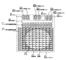
図3はボタン203、単位ディスプレイ205、配線206が形成されている基板212の上面図である。基板212の端部には接続用の端子211が備えられている。
【0032】
なお、プリント基板202上に設けられているコントローラーとメモリーは、基板212上に形成されていても良い。コントローラーとメモリーが、基板212上に形成されている場合の、基板212の上面図を図4に示す。
【0033】
図3において既に図示したものには同じ符号を付す。配線206はコントローラー215に接続されている。コントローラー215は各単位ディスプレイの駆動回路を駆動するのに用いられるクロック信号(CLK)やスタートパルス信号(SP)を生成する。またメモリー216に記憶されている記号の画像情報を読み出して、各単位ディスプレイのソース信号線駆動回路に入力する。
【0034】
なおメモリー216は各単位ディスプレイごとに設けても良い。
【0035】
単位ディスプレイ205の上面図を図5に示す。
【0036】
単位ディスプレイ205は、画素部214と、ソース信号線駆動回路217と、ゲート信号線駆動回路218とを有している。透光性のボタン203は画素部214上に設けられている。画素部214は複数の画素214を有しており、各画素はEL素子(図示せず)とTFT(図示せず)とをそれぞれ有している。
【0037】
なおメモリーを単位ディスプレイごとに設ける構成であっても良い。図6にメモリーが設けられた単位ディスプレイの上面図を示す。図5において既に図示したものには同じ符号を付す。
【0038】
図6に示す単位ディスプレイは、メモリーを3つ有している。なお単位ディスプレイごとに設けられるメモリーの数は、これに限定されない。メモリーの数は設計者が適宜設定することが可能である。
【0039】
図6に示す単位ディスプレイは、第1メモリー221、第2メモリー222、第3メモリー223と、第1〜3メモリーから記号の画像情報を読み出す選択回路220とを有している。第1メモリー221には数字の画像情報が記憶されており、第2メモリー222にはカナの画像情報が記憶されており、第3メモリー223にはアルファベットの画像情報が記憶されている。
【0040】
第1メモリー221は、縦表示用第1メモリー221aと、横表示用第1メモリー221bとを有している。縦表示用第1メモリー221aには縦方向の数字の画像情報が記憶されており、横表示用第1メモリー221bには横方向の数字の画像情報が記憶されている。
【0041】
第2メモリー222は、縦表示用第2メモリー222aと、横表示用第2メモリー222bとを有している。縦表示用第2メモリー222aには縦方向のカナの画像情報が記憶されており、横表示用第2メモリー222bには横方向のカナの画像情報が記憶されている。
【0042】
第3メモリー223は、縦表示用第3メモリー223aと、横表示用第3メモリー223bとを有している。縦表示用第3メモリー223aには縦方向のカナの画像情報が記憶されており、横表示用第3メモリー223bには横方向のカナの画像情報が記憶されている。
【0043】
例えば画素部214に数字を縦に表示させたい場合、選択回路220によって縦表示用第1メモリー221aから縦方向の数字の画像情報が読み出され、ソース信号線駆動回路218に入力される。
【0044】
なお、必ずしも1つの記号のみが、画素部214に表示されるわけではない。複数の記号が画素部214に表示されるように、複数の記号の画像情報が1つの画素部214に表示されるようにしても良い。
【0045】
第1〜3メモリーはフラッシュメモリーであっても、マスクROMであっても良い。図7に、単位ディスプレイが有するメモリーに用いられるマスクROMの構成を示す。
【0046】
マスクROMは複数のアドレス240がマトリクス状に設けられており、各アドレス240において選択用TFT241が設けられている。選択用TFT241のゲート電極は、走査線242に接続されている。選択用TFT241のソース領域とドレイン領域は、一方は読み出し用配線243に接続されており、もう一方は2つの電源のいずれか片方に接続されている。
【0047】
2つの電源は、一方は高電圧側電源(VDD)であり、もう一方は低電圧側電源(GND)である。各アドレス240において選択用TFT241が接続されている電源は、該メモリーが有する画像情報によって決まる。
【0048】
データ読み出しTFT244はゲート電極が選択線245に接続されている。データ読み出しTFT244のソース領域とドレイン領域は、一方は読み出し用配線243に、もう一方は出力線246に接続されている。
【0049】
選択用シフトレジスタ247から出力される選択用タイミング信号は、選択用バッファ248において増幅され、各走査線242に入力される。走査線242にゲート電極が接続された選択用TFT241は、選択用タイミング信号によってオンになり、電源(GNDまたはVDD)と読み出し用配線243とが電気的に導通する。
【0050】
次に読み出し用シフトレジスタ249から出力される読み出し用タイミング信号は、読み出し用バッファ250において増幅され、各選択線245に入力される。選択線245にゲート電極が接続されたデータ読み出し用TFT244は順にオンになり、読み出し用配線243を介して電源(GNDまたはVDD)の電位が出力線246に入力される。
【0051】
全てのアドレス240において上述した動作が行われることで、メモリーが有する画像情報を読み出すことができる。
【0052】
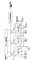
図8は本発明の電子装置の構成を説明するブロック図である。図8で示すシステムにおいて、キー入力部522には、単位ディスプレイ523とキー入力検知部524が備えられている。CPU506のキーボードインターフェイス部508はキーボードコントロール回路(コントローラー)520を介して単位ディスプレイ523が表示する記号の画像を制御する。
【0053】
また、キー入力検知部524からの信号は、入力信号処理回路521を介してキーボードインターフェイス部508に入力し、CPU506内部でデータ処理を行い、所定の情報をコントロール回路512に出力し、表示装置513にその情報を表示させたり送信をしたりする。
【0054】
その他の外部回路の構成は、安定化電源と高速高精度のオペアンプからなる電源504、音声処理回路502、外部インターフェイスポート505、送受信回路515などから成っている。また、CPU506には映像信号処理回路507が内蔵されている。また、CPU506にはVRAM511、DRAM509、フラッシュメモリー510及びメモリーカード503が接続されている。CPU503で処理された情報は、映像信号(データ信号)として映像信号処理回路507からコントロール回路512に出力する。コントロール回路512は、映像信号とクロックを表示装置513に供給する。具体的には、映像信号を表示装置の各画素に対応したデータに振り分ける機能と、外部から入力される水平同期信号及び垂直同期信号を、駆動回路のスタート信号及び内蔵電源回路の交流化のタイミング制御信号に変換する機能を持っている。
【0055】
図8で示すように、本発明の電子装置は、操作キーに設けられた複数の単位ディスプレイをCPUが集中して管理して制御する構成をとっている。
【0056】
図9を用いて、キーボードコントロール回路(コントローラー)520がソース信号駆動回路用のクロック信号(S−CLK)、スタートパルス信号(S−SP)と、ゲート信号駆動回路用のクロック信号(G−CLK)、スタートパルス信号(G−SP)とを生成する仕組みについて説明する。なお図9に示したコントローラーは、基準となるクロック信号の24倍の周期を有するS−SPを出力する。
【0057】
コントローラーはカウンタ回路261、262と、AND回路263、264とを有している。基準となるクロック信号(CLK)と、リセット信号(Res1)とがカウンタ回路261に入力されると、カウンタ回路261から4つの信号(out1〜4)がAND回路263に入力される。out1は基準となるクロック信号の周期を2倍にした信号であり、out2は同じく4倍、out3は同じく8倍、out4は同じく16倍にした信号である。
【0058】
out1はS−CLKとしてソース信号線駆動回路に入力される。またAND263から出力された信号はS−SPとしてソース信号線駆動回路に入力される。
【0059】
また、out1とリセット信号(Res2)はカウンタ回路262に入力される。そしてカウンタ回路262から4つの信号(out5〜8)がAND回路264に入力される。out5はout1の周期を2倍にした信号であり、out6は同じく4倍、out7は同じく8倍、out8は同じく16倍にした信号である。
【0060】
out5はG−CLKとしてゲート信号線駆動回路に入力される。またAND264から出力された信号はG−SPとしてゲート信号線駆動回路に入力される。
【0061】
本発明の単位ディスプレイは、単純マトリクス型、若しくはアクティブマトリクス型のいずれを採用することが可能である。
【0062】
単位ディスプレイに設けられるEL素子は、一対の電極(陽極と陰極)間に無機または有機EL材料(蛍光材料)から成る発光層を備えた構成をもっている。単位ディスプレイの画素部は特に限定されないが、10×10個または15×15個程度の画素をマトリクス状に配置して形成する。
【0063】
図12に本発明で用いられる単純マトリクス型の単位ディスプレイの画素部の構成を示す。
【0064】
基板2601上に陽極2602が短冊状に並べられて形成されている。そして基板2601上と陽極2602を覆ってマトリクス状に絶縁膜2603が形成されている。そして隣接するEL層及び陰極を分離するためのバンク2604が絶縁膜2603上に設けられている。
【0065】
バンク2604は隣接するEL層及び陰極を電気的に分離するためにも絶縁性の材料を用いて形成することが好ましい。
【0066】
そして基板2601、陽極2602、絶縁膜2603及びバンク2604を有するパッシブ基板上に、EL層2605と陰極2607とが順に積層して形成される。バンク2604を挟んで隣り合うEL層2605と陰極2607とは、バンク2604によって分離されている。EL層2605の材料は公知の材料を用いれば良く、ZnS:Mn、CdSSe、SrSなどの材料を用いて形成する。
【0067】
有機EL材料には低分子系(モノマー系)材料と高分子系(ポリマー系)材料があるがどちらを用いても良い。低分子系材料を用いる場合は蒸着法を用いるが、高分子系材料を用いる場合はスピンコート法や印刷法またはインクジェット法などを用いる。低分子系有機EL材料の一例は、正孔注入層として20nm厚の銅フタロシアニン(CuPc)膜を設け、その上に発光層として70nm厚のトリス−8−キノリノラトアルミニウム錯体(Alq3)膜を設けた積層構造としている。Alq3にキナクリドン、ペリレンもしくはDCM1といった蛍光色素を添加することで発光色を制御することができる。
【0068】
但し、以上の例はEL層として用いることのできる低分子系有機EL材料の一例であって、これに限定されるものではない。発光層、電荷輸送層または電荷注入層を自由に組み合わせてEL層(発光及びそのためのキャリアの移動を行わせるための層)を形成すれば良い。例えば、電荷輸送層や電荷注入層として炭化珪素等の無機材料を用いることも可能である。
【0069】
高分子系材料では、π共役ポリマー材料などが知られている。その代表例は結晶質半導体膜パラフェニレンビニレン(PPV)系、ポリビニルカルバゾール(PVK)系、ポリフルオレン系などが上げられる。このような材料を用いて形成されるEL層は、単層又は積層構造で用いられるが、積層構造で用いた方が発光効率は良い。一般的には陽極上に正孔注入層/正孔輸送層/発光層/電子輸送層の順に形成されるが、正孔輸送層/発光層/電子輸送層、または正孔注入層/正孔輸送層/発光層/電子輸送層/電子注入層のような構造でも良い。本発明では公知のいずれの構造を用いても良いし、EL層に対して蛍光性色素等をドーピングしても良い。
【0070】
カラー表示をする場合には大別して四つの方式があり、R(赤)G(緑)B(青)に対応した三種類のEL素子を形成する方式、白色発光のEL素子とカラーフィルターを組み合わせた方式、青色又は青緑発光のEL素子と蛍光体(蛍光性の色変換層:CCM)とを組み合わせた方式、陰極(対向電極)に透明電極を使用してRGBに対応したEL素子を重ねる方式がある。
【0071】
具体的なEL層としては、赤色に発光するEL層にはシアノポリフェニレン、緑色に発光するEL層にはポリフェニレンビニレン、青色に発光するEL層にはポリフェニレンビニレンまたはポリアルキルフェニレンを用いれば良い。EL層の厚さは30〜150nmとすれば良い。前記の例は発光層として用いることのできる有機EL材料の一例であり、これに限定されるものではない。発光層、電荷輸送層、電荷注入層を形成するための材料は、その可能な組合せにおいて自由に選択することができる。
【0072】
上記の例は発光層として用いることのできる有機EL材料の一例であり、これに限定されるものではない。発光層、電荷輸送層、電荷注入層を形成するための材料は、その可能な組合せにおいて自由に選択することができる。本実施の形態で示すEL層は、発光層とPEDOT(ポリチオフェン)またはPAni(ポリアニリン)から成る正孔注入層を設けた構造とする。
【0073】
単純マトリクス型はアクティブマトリクス型に比べて、作製方法が簡便であり、コストも低い。そのため、携帯情報端末自体のコストを低くすることが可能である。
【0074】
なお本発明の単位ディスプレイの画素部は、図12に示した構成に限定されない。
【0075】
図13はアクティブマトリクス型の単位ディスプレイの構造を示す一例を示している。TFTはチャネル形成領域を形成する半導体膜の材質により、アモルファスシリコンTFTやポリシリコンTFTと区別されることがあるが、そのいずれを採用しても構わない。
【0076】
基板601はガラス基板または有機樹脂基板が採用される。有機樹脂材料はガラス材料と比較して軽量であり、電子装置自体の軽量化に有効に作用する。単位ディスプレイを作製する上で適用できるものとしては、ポリイミド、ポリエチレンテレフタレート(PET)、ポリエチレンナフタレート(PEN)、ポリエーテルサルフォン(PES)、アラミドなどの有機樹脂材料を用いることができる。
【0077】
しかし、有機樹脂基板は、現在市場に供給されている材料の中で450℃以上の熱処理に耐えるものはない。しかし、レーザーアニール技術を使えば、基板加熱温度が300℃以下でもポリシリコンTFTを作製することが可能となる。また、ポリシリコンTFTの製造プロセスでは、水素化処理がしばしば必要とされるが、これはプラズマを援用した水素化処理を行うことで、200℃程度の基板温度でもその効果を得ることができる。
【0078】
図13では駆動回路650にnチャネル型TFT652とpチャネル型TFT653が形成され、画素部651にスイッチング用TFT654、EL駆動用TFT655が形成されている様子を示している。これらのTFTは、半導体層603〜606、ゲート絶縁膜607、ゲート電極608〜611などを用いて形成されている。
【0079】
基板601上に形成するブロッキング層602は基板601からオリゴマーなどが析出しないように、酸化窒化シリコン(SiOxNyで表される)、窒化シリコン膜などを50〜200nmの厚さに形成して設ける。層間絶縁膜は窒化シリコン、酸化窒化シリコンなどで形成される無機絶縁膜618と、アクリルまたはポリイミドなどで形成される有機絶縁膜619とから成っている。
【0080】
駆動回路部650の回路構成は、ゲート信号線駆動回路とソース信号線駆動回路とで異なるがここでは省略する。nチャネル型TFT652及びpチャネル型TFT653には配線612、613が接続され、これらのTFTを用いて、シフトレジスタやラッチ回路、バッファ回路などが形成される。
【0081】
画素部651では、ソース信号線614がスイッチング用TFT654のソース側に接続し、ドレイン側の配線615はEL駆動用TFT655のゲート電極611と接続している。また、EL駆動用TFT655のソース側は電源供給線617と接続し、ドレイン側の電極616がEL素子の陽極と接続するように配線されている。図14はこのような画素の上面図を示し、便宜上図13と共通する符号を用いて示している。また、図14において、A−A'線に対応する断面が図13において示されている。また、図14(B)はその等価回路を示している。
【0082】
単位ディスプレイは、図13に示すように、これら配線を覆うようにアクリルやポリイミドなどの有機樹脂、好適には感光性の有機樹脂を用いてバンク620、621が形成される。EL素子656は、ITO(酸化インジウム・スズ)で形成される陽極622、有機EL材料を用いて作製されるEL層623、MgAgやLiFなどのアルカリ金属またはアルカリ土類金属などの材料を用いて形成される陰極624とから成っている。バンク620、621は、陽極622の端部を覆うように形成され、この部分で陰極と陽極とがショートすることを防ぐために設ける。
【0083】
EL層623の上にはEL素子の陰極624が設けられる。陰極624としては、仕事関数の小さいマグネシウム(Mg)、リチウム(Li)若しくはカルシウム(Ca)を含む材料を用いる。好ましくはMgAg(MgとAgをMg:Ag=10:1で混合した材料)でなる電極を用いれば良い。他にもMgAgAl電極、LiAl電極、また、LiFAl電極が挙げられる。
【0084】
陰極624はEL層623を形成した後、大気解放しないで連続的に形成することが望ましい。陰極624とEL層623との界面状態はEL素子の発光効率に大きく影響するからである。なお、本明細書中では、陽極(画素電極)、EL層及び陰極で形成される発光素子をEL素子と呼ぶ。
【0085】
EL層623と陰極624とでなる積層体は、各画素で個別に形成する必要があるが、EL層623は水分に極めて弱いため、通常のフォトリソグラフィ技術を用いることができない。また、アルカリ金属を用いて作製される陰極424は容易に酸化されてしまう。従って、メタルマスク等の物理的なマスク材を用い、真空蒸着法、スパッタ法、プラズマCVD法等の気相法で選択的に形成することが好ましい。なお、EL層を選択的に形成する方法として、インクジェット法やスクリーン印刷法等を用いることも可能であるが、これらは現状では陰極の連続形成ができないので、上述の方法が好ましいと言える。
【0086】
また、陰極624上に外部の水分等から保護するための保護電極を積層しても良い。保護電極としては、アルミニウム(Al)、銅(Cu)若しくは銀(Ag)を含む低抵抗な材料を用いることが好ましい。或いは、透明電極を用いることで、図13において上方に光を放射させることもできる(これを便宜上、上面放射という)。その場合、有機樹脂層間絶縁膜絶縁膜611に黒色の顔料を混合させると、偏光板を用いなくても非発光時に黒色の画面を形成できる。この保護電極にはEL層の発熱を緩和する放熱効果も期待できる。また、上記EL層623、陰極624を形成した後、大気解放しないで連続的に保護電極まで形成することも有効である。
【0087】
三色に発光するEL素子を集積化したEL表示装置を用いると、例えば、使用者の好みに応じた色で照明させることや、着信時の呼び出し音と共に、登録されているグループ毎に照明の色を変えて、着信時の識別性を高めることもできる。EL素子の駆動電圧は1〜7V、好ましくは3Vであり、LSIの駆動電圧とほぼ同じ電圧で動作するので、昇圧回路を必要としない。
【0088】
いずれにしても、携帯電話装置など携帯型の電子装置において用いる場合には、少ない消費電力で高い輝度が得られることが要求される。EL層を形成する材料には、一重項励起子(シングレット)により発光する有機化合物(以下、シングレット化合物という)と、三重項励起子(トリプレット)により発光する有機化合物(以下、トリプレット化合物という)とがあり、これらを併用することも可能である。なお、シングレット化合物とは一重項励起のみを経由して発光する化合物を指し、トリプレット化合物とは三重項励起を経由して発光する化合物を指す。
【0089】
トリプレット化合物は、としては以下の論文に記載の有機化合物が代表的な材料として挙げられる。(1)T.Tsutsui, C.Adachi, S.Saito, Photochemical Processes in Organized Molecular Systems, ed.K.Honda, (Elsevier Sci.Pub., Tokyo,1991) p.437.(2)M.A.Baldo, D.F.O'Brien, Y.You, A.Shoustikov, S.Sibley, M.E.Thompson, S.R.Forrest, Nature 395 (1998) p.151.この論文には次の式で示される有機化合物が開示されている。(3)M.A.Baldo, S.Lamansky, P.E.Burrrows, M.E.Thompson, S.R.Forrest, Appl.Phys.Lett.,75 (1999) p.4.(4)T.Tsutsui, M.-J.Yang, M.Yahiro, K.Nakamura, T.Watanabe, T.tsuji, Y.Fukuda, T.Wakimoto, S.Mayaguchi, Jpn.Appl.Phys., 38 (12B) (1999) L1502.
【0090】
また、上記論文に記載された発光性材料だけでなく、次の分子式で表される発光性材料(具体的には金属錯体もしくは有機化合物)を用いることが可能であると考えている。
【0091】
【化1】

【化2】
上記分子式において、Mは周期表の8〜10族に属する元素である。上記論文では、白金、イリジウムが用いられている。また、本発明者はニッケル、コバルトもしくはパラジウムは、白金やイリジウムに比べて安価であるため、EL表示装置の製造コストを低減する上で好ましいと考えている。特に、ニッケルは錯体を形成しやすいため生産性も高く好ましいと考えられる。
【0094】
上記トリプレット化合物は、シングレット化合物よりも発光効率が高く、同じ発光輝度を得るにも動作電圧(EL素子を発光させるに要する電圧)を低くすることが可能である。
【0095】
例えば、赤色に発光する発光層として発光効率の高いトリプレット化合物を用いると、緑色に発光する発光層や青色に発光する発光層と同じ発光輝度を得ながらも動作電圧を揃えることが可能である。従って、赤色に発光する発光層の劣化が極端に早まることはなく、色ずれ等の問題を起こさずにカラー表示を行うことが可能となる。
【0096】
尚、ここでは赤色に発光する発光層としてトリプレット化合物を用いた例を示しているが、さらに緑色に発光する発光層もしくは青色に発光する発光層にトリプレット化合物を用いることも可能である。
【0097】
図13ではスイッチング用TFT654をマルチゲート構造とし、EL駆動用TFT655にはゲート電極とオーバーラップするLDDを設けている。ポリシリコンを用いたTFTは、高い動作速度を示すが故にホットキャリア注入などの劣化も起こりやすい。そのため、図13のように、画素内において機能に応じて構造の異なるTFT(オフ電流の十分に低いスイッチング用TFTと、ホットキャリア注入に強いEL駆動用TFT)を形成することは、高い信頼性を有し、且つ、良好な画像表示が可能な(動作性能の高い)表示装置を作製する上で非常に有効である。
【0098】
次にEL表示装置の接続端子の構造について説明する。
【0099】
EL表示装置の接続端子の構成には、何ら限定はないが、一例として、図15で示すようにチタン(Ti)とアルミニウム(Al)とから成る配線705と陽極として形成したITO706とを積層して形成している。図16は、接続端子部におけるA−A'線に対応する断面図を示している。基板701と封止基板702はシール材703で貼り合わされている。駆動回路において、EL層707、陰極708はバンク709上に形成されるが、陰極708を配線とコンタクトさせるため図示するようなコンタクト部710を設けている。
【0100】
次に、単位ディスプレイが有する駆動回路の構成について説明する。
【0101】
図17に示すように、単位ディスプレイはソース信号線駆動回路920、ゲート信号線駆動回路922、画素部900から成っている。
【0102】
ソース信号線駆動回路920は、シフトレジスタ920a、ラッチ(A)920b、ラッチ(B)920cを有している。ソース信号線駆動回路920において、シフトレジスタ920aにクロック信号(CLK)およびスタートパルス(SP)が入力される。シフトレジスタ920aは、これらのクロック信号(CLK)およびスタートパルス(SP)に基づきタイミング信号を順に発生させ、後段の回路へタイミング信号を順次供給する。
【0103】
なおシフトレジスタ920aからのタイミング信号を、バッファ等(図示せず)によって緩衝増幅し、後段の回路へ緩衝増幅したタイミング信号を順次供給しても良い。タイミング信号が供給される配線には、多くの回路あるいは素子が接続されているために負荷容量(寄生容量)が大きい。この負荷容量が大きいために生ずるタイミング信号の立ち上がりまたは立ち下がりの”鈍り”を防ぐために、このバッファが設けられる。
【0104】
シフトレジスタ920aからのタイミング信号は、ラッチ(A)920bに供給される。ラッチ(A)920bは、画像情報を有するデジタル信号(digital signals)を処理する複数のステージのラッチを有している。ラッチ(A)920bは、前記タイミング信号が入力されると同時に、デジタル信号を順次書き込み保持する。
【0105】
ラッチ(A)920bの全ステージのラッチへのデジタル信号の書き込みが一通り終了するまでの時間を、ライン期間と呼ぶ。すなわち、ラッチ(A)920b中で一番左側のステージのラッチにデジタル信号の書き込みが開始される時点から、一番右側のステージのラッチにデジタル信号の書き込みが終了する時点までの時間間隔がライン期間である。実際には、上記ライン期間に水平帰線期間が加えられた期間をライン期間に含むことがある。
【0106】
1ライン期間が終了すると、ラッチ(B)920cにラッチシグナル(Latch Signal)が供給される。この瞬間、ラッチ(A)920bに書き込まれ保持されているデジタル信号は、ラッチ(B)920cに一斉に送出され、ラッチ(B)920cの全ステージのラッチに書き込まれ、保持される。デジタル信号をラッチ(B)920cに送出し終えたラッチ(A)920bは、シフトレジスタ920aからのタイミング信号に基づき、再びデジタル信号の書き込みを順次行う。この2順目の1ライン期間中には、ラッチ(B)920bに書き込まれ、保持されているデジタル信号がソース信号線S1〜Sxに入力される。
【0107】
一方、ゲート信号線駆動回路922は、それぞれシフトレジスタ、バッファ(いずれも図示せず)を有している。また場合によっては、ゲート信号線駆動回路922が、シフトレジスタ、バッファの他にレベルシフトを有していても良い。ゲート信号線駆動回路922において、シフトレジスタ(図示せず)からのゲート信号がバッファ(図示せず)に供給され、対応するゲート信号線に供給される。ゲート信号線G1〜Gyには、それぞれ1ライン分の画素のスイッチング用TFTのゲート電極が接続されており、1ライン分全ての画素のスイッチング用TFTを同時にオンの状態にしなくてはならないので、バッファは大きな電流を流すことが可能なものが用いられる。尚、ソース信号線駆動回路とゲート信号線駆動回路の数、構成及びその動作は、本実施の形態で示した構成に限定されない。
【0108】
以上のようなキーボードを持つ本発明の電子装置は、画素部に表示される記号の方向及び操作キーに表示される記号の種類を、利用者が適宜変更することが可能である。例えば、図18(A)に示すように通常は数字を表しておく。利用者はメニューキーなどの操作により表示を切り替えると図18(B)に示すようにひらがな表示にしたり、図18(C)に示すようにアルファベット表示に切り替えることができる。操作キーに設けるEL素子をカラー表示可能としておくと、さらに色の情報を持たせることができる。そうすると、使用者の好みに応じた色で照明させることや、着信時の呼び出し音と共に、登録されているグループ毎に照明の色を変えて、着信時の識別性を高めることもできる。次に、図19に本発明により完成する電子装置の外観図の一例を示す。
【0109】
図19(A)には表示用パネル301と操作用パネル302とを横方向に並べたときに、表示部304に表示される画像の方向と、操作キー306に表示される文字、数字、記号等の画像の方向とが、利用者側から見て本来の方向にある場合を示している。
【0110】
図19(B)には表示用パネル301と操作用パネル302とを縦方向に並べたときに、表示部304に表示される画像の方向と、操作キー306に表示される文字、数字、記号等の画像の方向とが、利用者側から見て本来の方向にある場合を示している。
【0111】
本発明の電子装置は、利用者の使い勝手に合わせて、表示部304に表示される画像の方向及び操作キー306に表示される文字、数字、記号等の画像の方向を、図19(A)に示した方向と図19(B)に示した方向とに切り替えることが可能である。
【0112】
なお図19では表示部304に表示される画像の方向と、操作キー306に表示される文字、数字、記号等の画像の方向とが常に同じ場合について説明したが、本発明はこれに限定されない。表示部304に表示される画像の方向と、操作キー306に表示される文字、数字、記号等の画像の方向とが異なっていても良い。また、図19に示した操作キーが表示している文字、数字及び記号は一例であり、本発明の電子装置はこれらの文字、数字及び記号に限定されない。
【0113】
また、表示部304に表示される画像の方向と、操作キー306に表示される文字、数字、記号等の画像の方向とを、接続部303における表示用パネル301の表示部304を有する面と操作用パネル302の操作キー106を有する面との間の角度θによって自動的に変更するような構成にしても良い。
【0114】
また操作キーの表示の明暗を切り替えられるような構成にしても良い。図20(A)に示した操作キー356は白色の地に黒色の単数または複数の記号が表示されている。図20(B)に示した操作キー356は黒色の地に白色の単数または複数の記号が表示されている。
【0115】
なお図20(A)、図20(B)では、黒色または白色で表示を行う操作キーについて説明したが、本発明はこの構成に限定されない。操作キーが白色以外の色の表示を行っても良い。例えば黒色の地に黄色表示、白色の地に緑色表示、または青色の地に黒色表示を行っても構わない。
【0116】
上記構成によって、電子装置自体の消費電力を抑えることが可能である。
【0117】
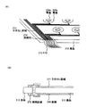
また、携帯電話装置はインターネットに接続して電子メールの送受信やホームページの検索などをすることが可能となっている。音声以外の文字情報は、操作キーを片手で操作して入力することが多い。その場合、利き手の親指または人差し指で操作キーを操作する。図20は図1で示す携帯電話装置の使用形態を説明する図である。インターネットに接続可能な携帯電話装置では、一画面に表示可能な画像情報量を増加させ、高精細化するために表示装置の大型化が成されている。しかし、画面の見やすさが向上するにつれ、使用者本人以外の第3者が表示された情報を見ることが容易となり、プライバシーが保たれなくなる。
【0118】
それに対し、本発明の携帯電話装置の操作キー106及び表示装置104の配置は、図21で示すように、操作キー106を操作しながら掌で表示装置104の画面をある程度覆い隠すことができるので、プライバシーを確保することができる。また、使用者にとっては安心感を持つことができる。
【0119】
また、表示装置104にイメージセンサーまたはエリアセンサーを内蔵させ、手のひらを表示装置104に覆いかぶせるようにして使用することにより、掌の紋章(手相)を用いて本人認証を行うことができる。認証は操作キー106でキー操作を行うとともに、使用者の手相をセンサー内蔵表示装置が個体情報を読み取り、認証作業を行う。認証作業はセンサーが読み取った個体情報と、内蔵するフラッシュメモリーや不揮発性メモリーに記憶されている個体情報とを照合して行う。
【0120】
尚、図21では操作キー106を親指で操作している例について示しているが、図22に示すように人差し指で操作する場合も同様である。
【0121】
また、本発明の電子装置の表示装置として用いられるELディスプレイと、単位ディスプレイに用いられるEL素子の輝度を、電子装置の外部の明るさに応じて調整するようにしても良い。
【0122】
図23に、電子装置の外部の明るさを検知するセンサの構成を示す。なお図23ではR(赤)、G(緑)、B(青)の3色のEL素子の輝度を調整する場合について説明するが、単色のEL素子の場合についても同様に実施することが可能である。
【0123】
センサ部1501は、RGBにそれぞれ対応したセンサ(R用センサ1501r、G用センサ1501g、B用センサ1501b)を有している。さらにそれぞれのセンサは、リセット用TFT1502、バッファ用TFT1503、ダイオード1504を有している。
【0124】
リセット用TFT1502のゲート電極はリセット信号線RLに接続されている。リセット用TFT1502のソース領域はセンサ用電源線VB及びバッファ用TFT1503のドレイン領域に接続されている。センサ用電源線は常に一定の電位(基準電位)に保たれている。またリセット用TFT1502のドレイン領域はダイオード1504及びバッファ用TFT1503のゲート電極に接続されている。
【0125】
バッファ用TFT1503のソース領域はセンサ出力配線FLに接続されている。またセンサ出力配線FLは定電流電源1505に接続されており、常に一定の電流が流れている。そしてバッファ用TFT1503のドレイン領域は常に一定の基準電位に保たれているセンサ用電源線VBに接続されており、バッファ用TFT1503はソースフォロワ(source follower)として機能する。
【0126】
図示しないが、ダイオード1504はカソードと、アノードと、カソードとアノードの間に設けられた光電変換層とを有している。
【0127】
リセット用TFT1502とバッファ用TFT1503は、どちらか一方がnチャネル型TFTで、残りの一方がpチャネル型TFTであることが望ましい。
【0128】
次にセンサ部1501において、ダイオード1504が外部の輝度を検知する仕組みについて説明する。
【0129】
まずリセット信号線RLに入力されたリセット信号によって、リセット用TFT1502がオンになる。よってセンサ用電源線VBの基準電位がバッファ用TFT1503のゲート電極に与えられる。そしてバッファ用TFT1503のソース領域はセンサ出力配線FLを介して定電流電源に接続されており、バッファ用TFT1503のソース領域とゲート電極の電位差VGSは常に一定である。よってバッファ用TFT1503のソース領域は、基準電位からVGSを差し引いた電位に保たれる。なお本明細書では、リセット用TFT1502がオンの状態である期間をリセット期間と呼ぶ。
【0130】
次にリセット信号線RLに入力されたリセット信号の電位が変化して、リセット用TFT1502がオフになる。よってセンサ用電源線VBの基準電位は、バッファ用TFT1503のゲート電極に与えられない。なお、リセット用TFT1502がオフの状態にある期間を、本明細書ではサンプル期間と呼ぶ。
【0131】
デジタル方式で駆動するELディスプレイの場合、サンプル期間はアドレス期間Taよりも長いことが好ましい。
【0132】
ダイオード1504に外部の光が照射されることで、ダイオード1504に電流が流れる。そのため、リセット期間において一定だったバッファ用TFT1503のゲート電極の電位は、サンプル期間において変化し、その電位の変化の大きさはダイオード1504に流れる電流の大きさによって変わる。
【0133】
ダイオード1504に流れる電流は、ダイオード1504に照射される光の強さに比例する。つまり外部が明るいときと暗いときとでは、明るいときの方が、ダイオード1504によりたくさん電流が流れることになる。よって、外部が明るいときの方が、暗いときに比べて、バッファ用TFT1503のゲート電極の電位は大きく変化する。
【0134】
バッファ用TFT1503のソース領域とゲート電極の電位差VGSは常に一定であるので、バッファ用TFT1503のソース領域は、バッファ用TFT1503のゲート電極の電位からVGSを差し引いた電位に保たれる。そのためバッファ用TFT1503のゲート電極の電位が変化すると、それに伴ってバッファ用TFT1503のソース領域の電位も変化する。
【0135】
バッファ用TFT1503のソース領域の電位はセンサ出力配線FLに与えられる。センサ出力配線FLの電位は、センサ選択回路1506によって順に選択された選択用TFT1507によって、センサ出力信号として輝度調整回路1508に入力される。
【0136】
図23に輝度調整回路1508のブロック図を示す。輝度調整回路1508はA/D変換回路1509、演算回路1510、補正メモリ1513、D/A変換回路1511を有している。なお、図23には補正メモリ1513が演算回路1510の一部である場合の構成を示したが、補正メモリ1513が演算回路1510と別個に設けられていても良い。
【0137】
センサ出力信号がA/D変換回路1509に入力されると、デジタルのセンサ出力信号に変換されて出力される。A/D変換回路1509から出力されたデジタルのセンサ出力信号は、演算回路1510に入力される。
【0138】
補正メモリ1513には、外部の輝度に対する、適切な電源供給線の電位の値(補正基準データ)が記憶されている。演算回路1510は、実際に演算回路1510に入力されたデジタルのセンサ出力信号から外部の輝度を割り出し、補正メモリ1513に記憶されている補正基準データを読み出す。
【0139】
そして読み出された補正基準データによって、EL素子が理想の輝度を得るために必要な電源供給線の電位(電源電位)の高さを情報として有するデジタルの補正信号が、D/A変換回路1511に入力する。
【0140】
D/A変換回路1511に入力されたデジタルの補正信号は、アナログに変換され、電源供給線の電源に入力される。電源供給線の電源は、入力されたアナログの補正信号によって定められた高さの電源電位を、電源供給線に与える。外部の輝度が変化した場合には、それに対応するように電源供給線の電源電位を補正し、使用者が見やすいように輝度を調整する。
【0141】
なおRGBに対応する3種類のEL素子を用いたELディスプレイの場合、輝度調整回路1508及び電源供給線の電源は補正したい色ごとに設ける必要がある。
【0142】
また、本発明は、図25に示すような液晶表示装置を表示装置に適用したノート型のコンピュータに適用することができる。図25(A)に示すコンピュータは本体1401、液晶表示装置を用いた表示装置1403、画像入力部1402、キーボード部1404を備えており、本発明はキーボード部1404に適用することができる。携帯性を重視した電子装置におけるキーボード部はキーの大きさや数に限界があり、本発明の操作キーを用いることにより、それぞれのキーに情報表示機能を持たせることで、データなどの入力作業を支援することができる。
【0143】
図25(B)に示す電話装置はファクシミリ機能が付加されたものでも良く、本体1410、受話器1411、電話番号などを表示する表示装置1412、操作キー1413などから成っている。本発明は操作キー1413に適用することが可能であり、このような据置型の電子装置においても利用者の入力作業を支援して利便性を高めることができる。
【0144】
図25では本発明が適用される電子装置の一例について示したが、その他にもディッスクトップ型コンピュータのキーボード、テレビ受像器やオーディオのリモコン、自動販売機の選択ボタン、様々な生産装置の制御盤に設けるスイッチなどあらゆる電子装置に適用できる。
【0145】
【発明の効果】
本発明の電子装置は、記号を入力するための操作キーに単位ディスプレイが設けられ、当該単位ディスプレイによって表示される記号の画像で、利用者が操作キーを識別することを可能としている。このような構成によって、限られた数の操作キーを有効利用することが可能となり、操作キーの多機能化と相まって利用者の便利性を高めることができる。
【0146】
さらに、電子装置の向きと、単位ディスプレイにより操作キーに表示される記号の向きとを、利用者が適宜変えること可能とし、操作性を向上させている。上記構成によって、電子装置の使い勝手を良くすることができる。
【図面の簡単な説明】
【図1】 携帯型の電子装置の一例を説明する図。
【図2】 本発明における電子装置の操作キーの構成を説明する図。
【図3】 本発明における電子装置の操作キーの構成を説明する図。
【図4】 本発明における電子装置の操作キーの構成を説明する図。
【図5】 単位ディスプレイの構成を説明する図。
【図6】 単位ディスプレイの構成を説明する図。
【図7】 マスクROMの構成を説明する図。
【図8】 本発明の電子装置の構成を説明するブロック図。
【図9】 コントローラーの構成を説明する図。
【図10】 タッチパネルの構成を説明する図。
【図11】 本発明における電子装置の操作キーの構成を説明する図。
【図12】 単純マトリクス型の画素部の構成を説明する図。
【図13】 単位ディスプレイの駆動回路と画素部の構成を説明する断面図。
【図14】 単位ディスプレイの画素部の構成を説明する上面図と等価回路図。
【図15】 単位ディスプレイの入力端子部の構成を説明する図。
【図16】 単位ディスプレイの入力端子部の構成を説明する図。
【図17】 単位ディスプレイの構成を説明するブロック図。
【図18】 本発明における電子装置の操作パネルの拡大図。
【図19】 本発明を用いた携帯型の電子装置の外観図。
【図20】 本発明における電子装置の操作パネルの拡大図。
【図21】 本発明を用いた携帯型の電子装置の操作形態について説明する図。
【図22】 本発明を用いた携帯型の電子装置の操作形態について説明する図。
【図23】 センサ部の構成を説明する図。
【図24】 センサ部から出力された信号によって輝度が補正される仕組みを説明する図。
【図25】 電子装置の一例を説明する図。
【図26】 引き出し配線の接続構成を示す図。[0001]
BACKGROUND OF THE INVENTION
The present invention is connected to an information terminal such as a stationary telephone, a facsimile, a personal computer, a portable information terminal represented by a mobile phone, a personal handy phone system (PHS), a PDA (Personal Digital Assistant), or the Internet. The present invention relates to an electronic device such as an information terminal that transmits and receives information. In this specification, a portable information terminal is an electronic device that can be carried by a user, and can transmit and receive data or information via a wireless telephone, a wired telephone, or the Internet outdoors or indoors. Refers to an electronic device.
[0002]
[Prior art]
A portable electronic device represented by a mobile phone device (or simply a mobile phone) establishes an information communication network using a telephone line such as a wireless communication line or the Internet, lowers a call charge or a body price, and its convenience. It is rapidly spreading due to its sex. A cellular phone device is integrally provided with a communication circuit, a display device, operation keys, a voice input unit, a voice output unit, an antenna that can be projected from the case, and the like.
[0003]
A portable electronic device typified by a cellular phone device has not only the appearance and function but also the weight and the length of continuous usable time (battery life) as the selection criteria of the user. For this reason, various ideas have been devised in order to reduce the weight of the portable electronic device and to increase the usable time by one charge. As a result, functions that seem unnecessary are removed as much as possible.
[0004]
[Problems to be solved by the invention]
For example, even in a mobile phone device capable of transmitting and receiving Internet mail, the number of operation keys is usually about 12 to 20 corresponding to numeric keys and special keys, and Japanese characters and special characters including kanji are used as data. In order to input, it was necessary to switch input modes and perform complicated operations.
[0005]
In view of such a fact, an object of the present invention is to provide a more convenient electronic device.
[0006]
[Means for Solving the Problems]
The present invention relates to a pixel having an EL element in each operation key for inputting information in an electronic device such as a portable information terminal typified by a mobile phone device, an information terminal typified by a personal computer or a stationary phone device. And a driving circuit for driving the pixel portion are provided. The pixel portion and the drive circuit included in each operation key are all integrally formed on the same substrate. It is characterized in that a user can identify an operation key by a symbol (including letters, numbers, and pictographs) displayed on each operation key by the pixel portion.
[0007]
With such a configuration, the user can identify the operation key even in a dark place. In this specification, a pixel portion and a drive circuit corresponding to each operation key are referred to as a unit display. All unit displays are formed on the same substrate. In this specification, all unit displays including the substrate are referred to as EL display devices.
[0008]
Note that the electronic device of the present invention may have a telephone function.
[0009]
Furthermore, in each operation key, the direction of the symbol displayed on the pixel portion can be switched according to the vertical and horizontal directions of the electronic device. The switching of the direction of the symbol can be realized by reading the image information of the symbol displayed in the vertical direction and the image information of the symbol displayed in the horizontal direction stored in the memory.
[0010]
As the unit display, either a simple matrix type or an active matrix type can be applied. The active matrix type is particularly preferable, and the pixel portion includes a plurality of pixels each having an EL element and a TFT. In order to increase the light emission efficiency of an EL element, it is applied as an effective means to form the light emitting layer of the EL element from a material containing a triplet exciton compound.
[0011]
With the above configuration, usability of the electronic device can be improved.
[0012]
DETAILED DESCRIPTION OF THE INVENTION
FIG. 1 shows an example of a cellular phone device that can be used in the present invention.
[0013]
The
[0014]
The
[0015]
The drive circuit, the memory, and other circuits can be arranged without increasing the area of the EL display device itself by being inserted between the operation keys.
[0016]
The symbol represented in the pixel portion can be recognized through a translucent button. FIG. 2 is a cross-sectional view for explaining the configuration of operation keys of a cellular phone device or PDA using the present invention.
[0017]
In FIG. 2A, a printed circuit board 202 made of glass epoxy resin or ceramic is inside a housing 201, and a baseband unit is a CPU (microprocessor), a DSP (digital signal processor), various memories. A signal processing circuit such as a (flash memory or SRAM), and a transmission / reception circuit unit equipped with a mixer, a frequency synthesizer, and the like are formed.
[0018]
An
[0019]
The operation
[0020]
The
[0021]
Between the
[0022]
As shown in FIG. 2A, in a normal state, the diaphragm 208 is in contact with only one
[0023]
A connection configuration of the
[0024]
As shown in FIG. 26B, a contact hole may be formed in the
[0025]
Note that it is also possible to detect the presence or absence of button operation using a touch panel without using a diaphragm.
[0026]
As shown in FIG. 10, the touch panel includes a
[0027]
A predetermined voltage is applied to the
[0028]
The
[0029]
FIG. 11 is a cross-sectional view of an operation key having the
[0030]
As shown in FIG. 11B, when the user presses the
[0031]
FIG. 3 is a top view of the
[0032]
The controller and the memory provided on the printed board 202 may be formed on the
[0033]
In FIG. 3, the same reference numerals are given to those already illustrated. The
[0034]
The
[0035]
A top view of the
[0036]
The
[0037]
In addition, the structure which provides a memory for every unit display may be sufficient. FIG. 6 shows a top view of a unit display provided with a memory. In FIG. 5, the same reference numerals are given to those already illustrated.
[0038]
The unit display shown in FIG. 6 has three memories. The number of memories provided for each unit display is not limited to this. The number of memories can be set as appropriate by the designer.
[0039]
The unit display shown in FIG. 6 includes a
[0040]
The
[0041]
The second memory 222 includes a vertical display
[0042]
The third memory 223 includes a vertical display
[0043]
For example, when it is desired to display numbers vertically in the
[0044]
Note that only one symbol is not necessarily displayed on the
[0045]
The first to third memories may be flash memories or mask ROMs. FIG. 7 shows a configuration of a mask ROM used for a memory included in the unit display.
[0046]
The mask ROM is provided with a plurality of addresses 240 in a matrix, and a
[0047]
One of the two power supplies is a high voltage power supply (VDD), and the other is a low voltage power supply (GND). The power source to which the
[0048]
The data read
[0049]
The selection timing signal output from the selection shift register 247 is amplified in the
[0050]
Next, the read timing signal output from the read shift register 249 is amplified in the read buffer 250 and input to each selection line 245. The
[0051]
By performing the above-described operation at all addresses 240, it is possible to read image information held in the memory.
[0052]
FIG. 8 is a block diagram illustrating the configuration of the electronic device of the present invention. In the system shown in FIG. 8, the
[0053]
A signal from the key
[0054]
The configuration of other external circuits includes a
[0055]
As shown in FIG. 8, the electronic apparatus of the present invention has a configuration in which a CPU centrally manages and controls a plurality of unit displays provided on operation keys.
[0056]
9, the keyboard control circuit (controller) 520 has a clock signal (S-CLK) for the source signal driving circuit, a start pulse signal (S-SP), and a clock signal (G-CLK for the gate signal driving circuit). ), A mechanism for generating the start pulse signal (G-SP) will be described. Note that the controller shown in FIG. Four An S-SP having a double period is output.
[0057]
The controller has
[0058]
out1 is input to the source signal line driver circuit as S-CLK. The signal output from the AND 263 is input to the source signal line driver circuit as S-SP.
[0059]
In addition, out1 and the reset signal (Res2) are input to the
[0060]
out5 is input to the gate signal line driver circuit as G-CLK. The signal output from the AND 264 is input to the gate signal line driver circuit as G-SP.
[0061]
The unit display of the present invention can adopt either a simple matrix type or an active matrix type.
[0062]
The EL element provided in the unit display has a configuration in which a light emitting layer made of an inorganic or organic EL material (fluorescent material) is provided between a pair of electrodes (anode and cathode). The pixel portion of the unit display is not particularly limited, but is formed by arranging about 10 × 10 or 15 × 15 pixels in a matrix.
[0063]
FIG. 12 shows a configuration of a pixel portion of a simple matrix type unit display used in the present invention.
[0064]
An
[0065]
The
[0066]
An
[0067]
Organic EL materials include low molecular (monomer) materials and high molecular (polymer) materials, either of which may be used. When a low molecular material is used, a vapor deposition method is used. When a high molecular material is used, a spin coating method, a printing method, an ink jet method, or the like is used. An example of a low molecular weight organic EL material is a 20 nm thick copper phthalocyanine (CuPc) film provided as a hole injection layer, and a 70 nm thick tris-8-quinolinolato aluminum complex (Alq) as a light emitting layer thereon. Three ) A laminated structure provided with a film. Alq Three The emission color can be controlled by adding a fluorescent dye such as quinacridone, perylene, or DCM1.
[0068]
However, the above example is an example of a low molecular weight organic EL material that can be used as an EL layer, and is not limited thereto. An EL layer (a layer for emitting light and moving carriers therefor) may be formed by freely combining a light-emitting layer, a charge transport layer, or a charge injection layer. For example, an inorganic material such as silicon carbide can be used for the charge transport layer and the charge injection layer.
[0069]
Among polymer materials, π-conjugated polymer materials are known. Typical examples thereof include crystalline semiconductor films such as paraphenylene vinylene (PPV), polyvinyl carbazole (PVK), and polyfluorene. An EL layer formed using such a material is used in a single layer or a stacked structure, but the light emission efficiency is better when the EL layer is used in a stacked structure. Generally, the hole injection layer / hole transport layer / light emitting layer / electron transport layer are formed on the anode in this order, but the hole transport layer / light emitting layer / electron transport layer, or hole injection layer / hole are formed. A structure such as a transport layer / a light emitting layer / an electron transport layer / an electron injection layer may be used. In the present invention, any known structure may be used, and the EL layer may be doped with a fluorescent dye or the like.
[0070]
There are four main methods for color display: a method of forming three types of EL elements corresponding to R (red), G (green), and B (blue), and a combination of white light-emitting EL elements and color filters. A combination of a blue or blue-green light emitting EL element and a phosphor (fluorescent color conversion layer: CCM), and using a transparent electrode on the cathode (counter electrode) to stack EL elements corresponding to RGB There is a method.
[0071]
As a specific EL layer, cyanopolyphenylene may be used for an EL layer that emits red light, polyphenylene vinylene may be used for an EL layer that emits green light, and polyphenylene vinylene or polyalkylphenylene may be used for an EL layer that emits blue light. The thickness of the EL layer may be 30 to 150 nm. The above example is an example of an organic EL material that can be used as a light emitting layer, and the present invention is not limited to this. The materials for forming the light emitting layer, the charge transport layer, and the charge injection layer can be freely selected in the possible combinations.
[0072]
The above example is an example of an organic EL material that can be used as a light emitting layer, and is not limited thereto. The materials for forming the light emitting layer, the charge transport layer, and the charge injection layer can be freely selected in the possible combinations. The EL layer described in this embodiment has a structure in which a light-emitting layer and a hole injection layer made of PEDOT (polythiophene) or PAni (polyaniline) are provided.
[0073]
The simple matrix type has a simpler manufacturing method and lower cost than the active matrix type. Therefore, it is possible to reduce the cost of the portable information terminal itself.
[0074]
Note that the pixel portion of the unit display of the present invention is not limited to the configuration shown in FIG.
[0075]
FIG. 13 shows an example of the structure of an active matrix unit display. A TFT may be distinguished from an amorphous silicon TFT or a polysilicon TFT depending on the material of a semiconductor film forming a channel formation region, either of which may be adopted.
[0076]
The
[0077]
However, there is no organic resin substrate that can withstand heat treatment at 450 ° C. or higher among materials currently on the market. However, if laser annealing technology is used, a polysilicon TFT can be fabricated even when the substrate heating temperature is 300 ° C. or lower. Further, in the manufacturing process of the polysilicon TFT, a hydrogenation treatment is often required, and this effect can be obtained even at a substrate temperature of about 200 ° C. by performing a hydrogenation treatment using plasma.
[0078]
FIG. 13 shows a state where an n-channel TFT 652 and a p-channel TFT 653 are formed in the driver circuit 650, and a switching
[0079]
The
[0080]
The circuit configuration of the driver circuit portion 650 differs between the gate signal line driver circuit and the source signal line driver circuit, but is omitted here.
[0081]
In the pixel portion 651, the
[0082]
As shown in FIG. 13, in the unit display,
[0083]
On the
[0084]
The
[0085]
A stacked body including the
[0086]
Further, a protective electrode for protecting from external moisture or the like may be stacked on the
[0087]
When an EL display device in which EL elements emitting three colors are integrated is used, for example, illumination is performed in a color according to the user's preference, and a ringing tone at the time of incoming call is used for each registered group. You can also change the color to increase the discriminability when receiving a call. The drive voltage of the EL element is 1 to 7 V, preferably 3 V, and operates at substantially the same voltage as the LSI drive voltage, so that a booster circuit is not required.
[0088]
In any case, when used in a portable electronic device such as a cellular phone device, it is required to obtain high luminance with low power consumption. The material forming the EL layer includes an organic compound that emits light by singlet excitons (hereinafter referred to as a singlet compound), and an organic compound that emits light by triplet excitons (hereinafter referred to as a triplet), and These can be used in combination. The singlet compound refers to a compound that emits light only through singlet excitation, and the triplet compound refers to a compound that emits light via triplet excitation.
[0089]
Examples of the triplet compound include organic compounds described in the following papers as typical materials. (1) T. Tsutsui, C. Adachi, S. Saito, Photochemical Processes in Organized Molecular Systems, ed. K. Honda, (Elsevier Sci. Pub., Tokyo, 1991) p.437. (2) MABaldo, DFO ' Brien, Y.You, A.Shoustikov, S.Sibley, METhompson, SRForrest, Nature 395 (1998) p.151. This paper discloses an organic compound represented by the following formula. (3) MABaldo, S. Lamansky, PEBurrrows, METhompson, SRForrest, Appl. Phys. Lett., 75 (1999) p. 4. (4) T. Tsutsui, M.-J. Yang, M. Yahiro, K. Nakamura, T. Watanabe, T. tsuji, Y. Fukuda, T. Wakimoto, S. Mayaguchi, Jpn. Appl. Phys., 38 (12B) (1999) L1502.
[0090]
In addition to the luminescent material described in the above paper, it is considered possible to use a luminescent material represented by the following molecular formula (specifically, a metal complex or an organic compound).
[0091]
[Chemical 1]
[Chemical 2]
In the above molecular formula, M is an element belonging to
[0094]
The triplet compound has higher luminous efficiency than the singlet compound, and the operating voltage (voltage required for causing the EL element to emit light) can be lowered to obtain the same light emission luminance.
[0095]
For example, when a triplet compound having high emission efficiency is used as the light emitting layer that emits red light, the operating voltage can be made uniform while obtaining the same light emission luminance as the light emitting layer that emits green light or the light emitting layer that emits blue light. Therefore, the deterioration of the light emitting layer emitting red light is not accelerated rapidly, and color display can be performed without causing problems such as color misregistration.
[0096]
Here, an example in which a triplet compound is used as a light emitting layer emitting red light is shown, but a triplet compound can also be used for a light emitting layer emitting green light or a light emitting layer emitting blue light.
[0097]
In FIG. 13, the switching
[0098]
Next, the structure of the connection terminal of the EL display device will be described.
[0099]
The structure of the connection terminal of the EL display device is not limited at all. For example, as shown in FIG. 15, a
[0100]
Next, the configuration of the drive circuit included in the unit display will be described.
[0101]
As shown in FIG. 17, the unit display includes a source signal line driving circuit 920, a gate signal
[0102]
The source signal line driver circuit 920 includes a shift register 920a, a latch (A) 920b, and a latch (B) 920c. In the source signal line driver circuit 920, a clock signal (CLK) and a start pulse (SP) are input to the shift register 920a. The shift register 920a sequentially generates timing signals based on the clock signal (CLK) and the start pulse (SP), and sequentially supplies the timing signals to subsequent circuits.
[0103]
Note that the timing signal from the shift register 920a may be buffered and amplified by a buffer or the like (not shown), and the buffered timing signal may be sequentially supplied to a subsequent circuit. Since many circuits or elements are connected to the wiring to which the timing signal is supplied, the load capacitance (parasitic capacitance) is large. This buffer is provided in order to prevent “blunting” of the rising edge or falling edge of the timing signal caused by the large load capacity.
[0104]
The timing signal from the shift register 920a is supplied to the latch (A) 920b. The latch (A) 920b includes a plurality of stages of latches for processing digital signals having image information. The latch (A) 920b sequentially writes and holds digital signals at the same time as the timing signal is input.
[0105]
The time until digital signal writing to all the latches of the latch (A) 920b is completed is called a line period. That is, the time interval from the time when the writing of the digital signal to the latch of the leftmost stage in the latch (A) 920b is started until the time when the writing of the digital signal to the latch of the rightmost stage is completed is line. It is a period. Actually, the line period may include a period obtained by adding a horizontal blanking period to the line period.
[0106]
When one line period ends, a latch signal (Latch Signal) is supplied to the latch (B) 920c. At this moment, the digital signals written and held in the latch (A) 920b are sent all at once to the latch (B) 920c, and are written and held in the latches of all the stages of the latch (B) 920c. The latch (A) 920b which has finished sending the digital signal to the latch (B) 920c sequentially writes the digital signal again based on the timing signal from the shift register 920a. During this second line of one line period, the digital signals written and held in the latch (B) 920b are input to the source signal lines S1 to Sx.
[0107]
On the other hand, each of the gate signal
[0108]
In the electronic apparatus of the present invention having the keyboard as described above, the user can appropriately change the direction of the symbol displayed on the pixel portion and the type of the symbol displayed on the operation key. For example, numbers are usually represented as shown in FIG. When the user switches the display by operating the menu key or the like, the user can switch to the hiragana display as shown in FIG. 18B or the alphabet display as shown in FIG. If the EL element provided in the operation key can be displayed in color, further color information can be provided. In this case, it is possible to illuminate with a color according to the user's preference, and to change the color of the illumination for each registered group together with the ringing tone at the time of incoming call, thereby enhancing the discriminability at the time of incoming call. Next, FIG. 19 shows an example of an external view of an electronic device completed according to the present invention.
[0109]
In FIG. 19A, when the
[0110]
FIG. 19B shows the direction of the image displayed on the display portion 304 and the characters, numbers, and symbols displayed on the
[0111]
In the electronic device of the present invention, the direction of an image displayed on the display unit 304 and the direction of an image such as characters, numbers, and symbols displayed on the
[0112]
Note that FIG. 19 illustrates the case where the direction of the image displayed on the display unit 304 is always the same as the direction of the image such as letters, numbers, and symbols displayed on the
[0113]
Further, the direction of the image displayed on the display unit 304 and the direction of the image such as characters, numbers, and symbols displayed on the
[0114]
Further, it may be configured such that the display of the operation key can be switched between light and dark. The operation key 356 shown in FIG. 20A has a black symbol or symbols displayed on a white background. In the operation key 356 shown in FIG. 20B, a white symbol or symbols are displayed on a black background.
[0115]
In FIGS. 20A and 20B, the operation keys for displaying in black or white have been described, but the present invention is not limited to this configuration. The operation key may display a color other than white. For example, yellow display on a black background, green display on a white background, or black display on a blue background may be performed.
[0116]
With the above configuration, power consumption of the electronic device itself can be suppressed.
[0117]
In addition, the mobile phone device can be connected to the Internet to send and receive e-mails and search home pages. Character information other than voice is often input by operating an operation key with one hand. In that case, the operation key is operated with the thumb or index finger of the dominant hand. FIG. 20 is a diagram for explaining a usage pattern of the mobile phone device shown in FIG. In mobile phone devices that can be connected to the Internet, the size of display devices has been increased in order to increase the amount of image information that can be displayed on one screen and to achieve higher definition. However, as the visibility of the screen improves, it becomes easier for a third party other than the user to view the displayed information, and privacy cannot be maintained.
[0118]
On the other hand, the arrangement of the
[0119]
Further, by using an image sensor or an area sensor incorporated in the
[0120]
21 shows an example in which the
[0121]
Moreover, you may make it adjust the brightness | luminance of the EL display used as a display apparatus of the electronic device of this invention, and the EL element used for a unit display according to the external brightness of an electronic device.
[0122]
FIG. 23 shows the configuration of a sensor that detects the brightness outside the electronic device. Note that FIG. 23 illustrates the case of adjusting the luminance of the EL elements of three colors R (red), G (green), and B (blue), but the same can be applied to the case of a single color EL element. It is.
[0123]
The
[0124]
The gate electrode of the reset TFT 1502 is connected to the reset signal line RL. The source region of the reset TFT 1502 is connected to the sensor power supply line VB and the drain region of the
[0125]
The source region of the
[0126]
Although not shown, the
[0127]
One of the reset TFT 1502 and the
[0128]
Next, a mechanism in which the
[0129]
First, the reset TFT 1502 is turned on by the reset signal input to the reset signal line RL. Therefore, the reference potential of the sensor power supply line VB is applied to the gate electrode of the
[0130]
Next, the potential of the reset signal input to the reset signal line RL changes, and the reset TFT 1502 is turned off. Therefore, the reference potential of the sensor power supply line VB is not applied to the gate electrode of the
[0131]
In the case of an EL display driven in a digital manner, the sample period is preferably longer than the address period Ta.
[0132]
A current flows through the
[0133]
The current flowing through the
[0134]
Potential difference V between source region and gate electrode of
[0135]
The potential of the source region of the
[0136]
FIG. 23 shows a block diagram of the luminance adjustment circuit 1508. The luminance adjustment circuit 1508 includes an A / D conversion circuit 1509, an
[0137]
When the sensor output signal is input to the A / D conversion circuit 1509, it is converted into a digital sensor output signal and output. A digital sensor output signal output from the A / D conversion circuit 1509 is input to the
[0138]
The
[0139]
Based on the read correction reference data, a digital correction signal having, as information, the height of the potential of the power supply line (power supply potential) necessary for the EL element to obtain an ideal luminance is used as the D / A conversion circuit 1511. To enter.
[0140]
The digital correction signal input to the D / A conversion circuit 1511 is converted to analog and input to the power supply of the power supply line. The power supply of the power supply line supplies a power supply potential having a height determined by the input analog correction signal to the power supply line. When the external brightness changes, the power supply potential of the power supply line is corrected so as to cope with it, and the brightness is adjusted so that the user can easily see it.
[0141]
Note that in the case of an EL display using three types of EL elements corresponding to RGB, the luminance adjustment circuit 1508 and the power source of the power supply line need to be provided for each color to be corrected.
[0142]
Further, the present invention can be applied to a notebook computer in which a liquid crystal display device as shown in FIG. 25 is applied to a display device. A computer shown in FIG. 25A includes a main body 1401, a display device 1403 using a liquid crystal display device, an image input portion 1402, and a
[0143]
The telephone device shown in FIG. 25B may be provided with a facsimile function, and includes a
[0144]
FIG. 25 shows an example of an electronic apparatus to which the present invention is applied. In addition, a keyboard of a desktop computer, a television receiver or an audio remote controller, a selection button of a vending machine, and control of various production apparatuses. It can be applied to all electronic devices such as switches provided on the panel.
[0145]
【The invention's effect】
In the electronic device of the present invention, a unit display is provided on an operation key for inputting a symbol, and the user can identify the operation key by an image of the symbol displayed by the unit display. With such a configuration, it is possible to effectively use a limited number of operation keys, and the convenience of the user can be enhanced in combination with the multifunctional operation keys.
[0146]
Furthermore, the direction of the electronic device and the direction of the symbols displayed on the operation keys by the unit display can be appropriately changed by the user, thereby improving the operability. With the above configuration, usability of the electronic device can be improved.
[Brief description of the drawings]
FIG. 1 illustrates an example of a portable electronic device.
FIG. 2 is a diagram illustrating a configuration of operation keys of an electronic device according to the present invention.
FIG. 3 is a diagram illustrating a configuration of operation keys of an electronic device according to the present invention.
FIG. 4 is a diagram illustrating a configuration of operation keys of an electronic device according to the present invention.
FIG. 5 is a diagram illustrating a configuration of a unit display.
FIG. 6 is a diagram illustrating a configuration of a unit display.
FIG. 7 illustrates a configuration of a mask ROM.
FIG. 8 is a block diagram illustrating a structure of an electronic device of the invention.
FIG. 9 is a diagram illustrating the configuration of a controller.
FIG 10 illustrates a structure of a touch panel.
FIG. 11 is a diagram illustrating a configuration of operation keys of an electronic device according to the present invention.
FIG. 12 illustrates a structure of a simple matrix pixel portion.
FIG. 13 is a cross-sectional view illustrating a configuration of a driving circuit and a pixel portion of a unit display.
FIG. 14 is a top view and an equivalent circuit diagram illustrating a configuration of a pixel portion of a unit display.
FIG. 15 is a diagram illustrating a configuration of an input terminal portion of a unit display.
FIG. 16 is a diagram illustrating a configuration of an input terminal portion of a unit display.
FIG. 17 is a block diagram illustrating the configuration of a unit display.
FIG. 18 is an enlarged view of an operation panel of the electronic device according to the present invention.
FIG. 19 is an external view of a portable electronic device using the present invention.
FIG. 20 is an enlarged view of an operation panel of the electronic device according to the present invention.
FIG. 21 is a diagram illustrating an operation mode of a portable electronic device using the invention.
FIG. 22 illustrates an operation mode of a portable electronic device using the invention.
FIG. 23 is a diagram illustrating a configuration of a sensor unit.
FIG. 24 is a diagram illustrating a mechanism in which luminance is corrected by a signal output from a sensor unit.
FIG 25 illustrates an example of an electronic device.
FIG. 26 is a diagram showing a connection configuration of lead wires.
Claims (12)
複数の前記ボタンの操作の有無を検知する検知手段と、Detecting means for detecting presence or absence of operation of a plurality of the buttons;
複数の前記ボタンに対応して設けられた複数の単位ディスプレイと、を備えた操作キーを有し、A plurality of unit displays provided corresponding to the plurality of buttons, and an operation key comprising:
前記検知手段は、複数の前記単位ディスプレイと複数の前記ボタンとの間に配置されており、The detection means is disposed between the plurality of unit displays and the plurality of buttons.
複数の前記単位ディスプレイは、全て同一のガラス基板上に形成されたものであることを特徴とする電子装置。The plurality of unit displays are all formed on the same glass substrate.
前記検知手段は、一対の電極とダイアフラムとを複数有し、The detection means includes a plurality of pairs of electrodes and diaphragms,
複数の前記単位ディスプレイは、前記ガラス基板の一方の面に形成されたものであり、The plurality of unit displays are formed on one surface of the glass substrate,
複数の前記一対の電極は、前記ガラス基板の他方の面に形成されたものであり、The plurality of the pair of electrodes are formed on the other surface of the glass substrate,
複数の前記ダイアフラムはそれぞれ、複数の前記ボタンと複数の前記一対の電極との間に配置されており、Each of the plurality of diaphragms is disposed between the plurality of buttons and the plurality of pairs of electrodes,
前記ダイアフラムは、前記一対の電極と重なる位置に配置されているとともに、前記一対の電極の一方と接触していることを特徴とする電子装置。The diaphragm is disposed at a position overlapping the pair of electrodes and is in contact with one of the pair of electrodes.
前記検知手段は、タッチパネルであることを特徴とする電子装置。The electronic device is characterized in that the detection means is a touch panel.
複数の前記単位ディスプレイを制御するCPUが設けられたプリント基板を有し、A printed circuit board provided with a CPU for controlling a plurality of the unit displays;
複数の前記単位ディスプレイは、前記検知手段と前記プリント基板との間に設けられており、The plurality of unit displays are provided between the detection means and the printed circuit board,
複数の前記ボタンと、前記検知手段と、複数の前記単位ディスプレイと、前記プリント基板と、は重なるように配置されていることを特徴とする電子装置。The electronic device, wherein the plurality of buttons, the detection means, the plurality of unit displays, and the printed circuit board are arranged to overlap each other.
表示部と音声入力部とが設けられた第1のパネルと、A first panel provided with a display unit and a voice input unit;
前記操作キーと音声出力部とが設けられた第2のパネルと、を有し、A second panel provided with the operation keys and a voice output unit,
前記第1のパネルと前記第2のパネルとは連結されており、The first panel and the second panel are connected,
前記表示部には掌の紋章の認証を行うためのエリアセンサーが内蔵されていることを特徴とする電子装置。An electronic device, wherein the display unit includes an area sensor for authenticating a palm crest.
前記表示部が前記掌に覆われた状態で、前記操作キーを用いた第1の操作が行われることを特徴とする電子装置。An electronic apparatus in which a first operation using the operation keys is performed in a state where the display unit is covered with the palm.
前記表示部が前記掌に覆われた状態且つ前記操作キーを用いた第2の操作が行われている状態で、前記認証が行われることを特徴とする電子装置。The electronic device is characterized in that the authentication is performed in a state where the display unit is covered with the palm and a second operation using the operation key is performed.
複数の前記単位ディスプレイに表示される第1の記号の上方向が前記音声入力部から前記音声出力部へ向かう第1の方向と一致し、且つ、前記表示部に表示される第2の記号の上方向が前記第1の方向と一致する第1の設定状態を有することを特徴とする電子装置。The upper direction of the first symbol displayed on the plurality of unit displays matches the first direction from the voice input unit to the voice output unit, and the second symbol displayed on the display unit An electronic apparatus having a first setting state in which an upward direction coincides with the first direction.
複数の前記単位ディスプレイに表示される第1の記号の上方向が前記音声入力部から前記音声出力部へ向かう第1の方向と一致し、且つ、前記表示部に表示される第2の記号の上方向が前記第1の方向と一致する第1の設定状態と、The upper direction of the first symbol displayed on the plurality of unit displays matches the first direction from the voice input unit to the voice output unit, and the second symbol displayed on the display unit A first setting state in which an upward direction matches the first direction;
前記第1の記号の上方向が前記第1の方向と垂直な第2の方向と一致し、且つ、前記第2の記号の上方向が前記第2の方向と一致する第2の設定状態と、の切り替えが行われることを特徴とする電子装置。A second setting state in which the upward direction of the first symbol coincides with a second direction perpendicular to the first direction, and the upward direction of the second symbol coincides with the second direction; The electronic device is characterized in that switching is performed.
前記第1のパネルの前記表示部を有する面と、前記第2のパネルの前記操作キーと、の角度に応じて前記第1の設定状態と前記第2の設定状態とが切り替わることを特徴とする電子装置。The first setting state and the second setting state are switched according to an angle between a surface of the first panel having the display unit and the operation key of the second panel. Electronic device to play.
前記第1のパネルにアンテナが設けられていることを特徴とする電子装置。An electronic device, wherein an antenna is provided on the first panel.
複数の前記単位ディスプレイの表示の明暗の切り替えが可能なことを特徴とする電子装置。An electronic device characterized in that the display of the plurality of unit displays can be switched between light and dark.
Priority Applications (1)
| Application Number | Priority Date | Filing Date | Title |
|---|---|---|---|
| JP2001278944A JP4758039B2 (en) | 2000-09-14 | 2001-09-14 | Electronic equipment |
Applications Claiming Priority (4)
| Application Number | Priority Date | Filing Date | Title |
|---|---|---|---|
| JP2000280047 | 2000-09-14 | ||
| JP2000280047 | 2000-09-14 | ||
| JP2000-280047 | 2000-09-14 | ||
| JP2001278944A JP4758039B2 (en) | 2000-09-14 | 2001-09-14 | Electronic equipment |
Publications (3)
| Publication Number | Publication Date |
|---|---|
| JP2002175144A JP2002175144A (en) | 2002-06-21 |
| JP2002175144A5 JP2002175144A5 (en) | 2008-10-16 |
| JP4758039B2 true JP4758039B2 (en) | 2011-08-24 |
Family
ID=26600001
Family Applications (1)
| Application Number | Title | Priority Date | Filing Date |
|---|---|---|---|
| JP2001278944A Expired - Fee Related JP4758039B2 (en) | 2000-09-14 | 2001-09-14 | Electronic equipment |
Country Status (1)
| Country | Link |
|---|---|
| JP (1) | JP4758039B2 (en) |
Families Citing this family (1)
| Publication number | Priority date | Publication date | Assignee | Title |
|---|---|---|---|---|
| KR101266248B1 (en) * | 2006-08-07 | 2013-05-22 | 삼성디스플레이 주식회사 | Display Device, Method of Manufacturing The Same And Mobile Communication Terminal Having The Same |
Family Cites Families (6)
| Publication number | Priority date | Publication date | Assignee | Title |
|---|---|---|---|---|
| JPS617913A (en) * | 1984-06-22 | 1986-01-14 | Tadakore Kajiyama | Key input device and its assembling method |
| JPS6282454A (en) * | 1985-10-08 | 1987-04-15 | Canon Inc | Electronic equipment |
| JPS6375820A (en) * | 1986-09-18 | 1988-04-06 | Anritsu Corp | Multi-item information input device |
| JPH0817283A (en) * | 1994-06-30 | 1996-01-19 | Achilles Corp | Rubber contact switch |
| JPH09321846A (en) * | 1996-05-29 | 1997-12-12 | Yazaki Corp | Portable terminal equipment |
| JPH11329739A (en) * | 1998-05-11 | 1999-11-30 | Oki Electric Ind Co Ltd | Organic el element and production of the same |
-
2001
- 2001-09-14 JP JP2001278944A patent/JP4758039B2/en not_active Expired - Fee Related
Also Published As
| Publication number | Publication date |
|---|---|
| JP2002175144A (en) | 2002-06-21 |
Similar Documents
| Publication | Publication Date | Title |
|---|---|---|
| US9112963B2 (en) | Electronic device and method of usage thereof | |
| JP6611881B2 (en) | Light emitting device | |
| US6680577B1 (en) | EL display device and electronic apparatus | |
| US8644498B2 (en) | Electronic device | |
| US20180175119A1 (en) | Light-Emitting Device | |
| JP2022106858A (en) | Display device | |
| TWI242391B (en) | Light emitting device | |
| JP4718731B2 (en) | Electronic equipment | |
| TWI250498B (en) | Display device and electric equipment using the same | |
| US20090026969A1 (en) | Organic light emitting device | |
| US20090002280A1 (en) | Organic light emitting device and method of driving the same | |
| KR20120034706A (en) | Display device | |
| CN109728174A (en) | Organic electroluminescent device, Organnic electroluminescent device and electronic equipment | |
| US20240065028A1 (en) | Display device and pixel array substrate thereof | |
| JP4758039B2 (en) | Electronic equipment | |
| WO2003091982A1 (en) | Display device and electronic apparatus | |
| JP4906145B2 (en) | EL display device | |
| JP2001339492A (en) | Electronic equipment | |
| JP2006058898A (en) | Display panel driving driver of light emitting display device, and light emitting display device, and driving method for display panel of light emitting display device | |
| JP4314000B2 (en) | Display device | |
| JP3583413B2 (en) | Switch element, display device and semiconductor device using the same | |
| KR101572264B1 (en) | Organic Light Emitting Display Device and Manufacturing Method of the same | |
| KR100603401B1 (en) | Active matrix type electroluminescent display device and mobile apparatus therewith | |
| CN106972107A (en) | Organic Light Emitting Diode and the organic LED display device including it | |
| KR100669771B1 (en) | Active matrix light emitting diode display and mobile apparatus therewith |
Legal Events
| Date | Code | Title | Description |
|---|---|---|---|
| A521 | Request for written amendment filed |
Free format text: JAPANESE INTERMEDIATE CODE: A523 Effective date: 20080829 |
|
| A621 | Written request for application examination |
Free format text: JAPANESE INTERMEDIATE CODE: A621 Effective date: 20080829 |
|
| A977 | Report on retrieval |
Free format text: JAPANESE INTERMEDIATE CODE: A971007 Effective date: 20100827 |
|
| A131 | Notification of reasons for refusal |
Free format text: JAPANESE INTERMEDIATE CODE: A131 Effective date: 20101221 |
|
| A521 | Request for written amendment filed |
Free format text: JAPANESE INTERMEDIATE CODE: A523 Effective date: 20110131 |
|
| TRDD | Decision of grant or rejection written | ||
| A01 | Written decision to grant a patent or to grant a registration (utility model) |
Free format text: JAPANESE INTERMEDIATE CODE: A01 Effective date: 20110524 |
|
| A01 | Written decision to grant a patent or to grant a registration (utility model) |
Free format text: JAPANESE INTERMEDIATE CODE: A01 |
|
| A61 | First payment of annual fees (during grant procedure) |
Free format text: JAPANESE INTERMEDIATE CODE: A61 Effective date: 20110602 |
|
| R150 | Certificate of patent or registration of utility model |
Ref document number: 4758039 Country of ref document: JP Free format text: JAPANESE INTERMEDIATE CODE: R150 Free format text: JAPANESE INTERMEDIATE CODE: R150 |
|
| FPAY | Renewal fee payment (event date is renewal date of database) |
Free format text: PAYMENT UNTIL: 20140610 Year of fee payment: 3 |
|
| FPAY | Renewal fee payment (event date is renewal date of database) |
Free format text: PAYMENT UNTIL: 20140610 Year of fee payment: 3 |
|
| R250 | Receipt of annual fees |
Free format text: JAPANESE INTERMEDIATE CODE: R250 |
|
| R250 | Receipt of annual fees |
Free format text: JAPANESE INTERMEDIATE CODE: R250 |
|
| R250 | Receipt of annual fees |
Free format text: JAPANESE INTERMEDIATE CODE: R250 |
|
| R250 | Receipt of annual fees |
Free format text: JAPANESE INTERMEDIATE CODE: R250 |
|
| R250 | Receipt of annual fees |
Free format text: JAPANESE INTERMEDIATE CODE: R250 |
|
| R250 | Receipt of annual fees |
Free format text: JAPANESE INTERMEDIATE CODE: R250 |
|
| R250 | Receipt of annual fees |
Free format text: JAPANESE INTERMEDIATE CODE: R250 |
|
| LAPS | Cancellation because of no payment of annual fees |