JP4745477B2 - Electrostatic discharge protection for sensors - Google Patents
Electrostatic discharge protection for sensors Download PDFInfo
- Publication number
- JP4745477B2 JP4745477B2 JP36093299A JP36093299A JP4745477B2 JP 4745477 B2 JP4745477 B2 JP 4745477B2 JP 36093299 A JP36093299 A JP 36093299A JP 36093299 A JP36093299 A JP 36093299A JP 4745477 B2 JP4745477 B2 JP 4745477B2
- Authority
- JP
- Japan
- Prior art keywords
- layer
- conductive
- sensor
- dielectric layer
- passivation
- Prior art date
- Legal status (The legal status is an assumption and is not a legal conclusion. Google has not performed a legal analysis and makes no representation as to the accuracy of the status listed.)
- Expired - Lifetime
Links
Images


Classifications
-
- G—PHYSICS
- G06—COMPUTING; CALCULATING OR COUNTING
- G06V—IMAGE OR VIDEO RECOGNITION OR UNDERSTANDING
- G06V40/00—Recognition of biometric, human-related or animal-related patterns in image or video data
- G06V40/10—Human or animal bodies, e.g. vehicle occupants or pedestrians; Body parts, e.g. hands
- G06V40/12—Fingerprints or palmprints
- G06V40/13—Sensors therefor
- G06V40/1329—Protecting the fingerprint sensor against damage caused by the finger
Landscapes
- Engineering & Computer Science (AREA)
- Human Computer Interaction (AREA)
- Physics & Mathematics (AREA)
- General Physics & Mathematics (AREA)
- Multimedia (AREA)
- Theoretical Computer Science (AREA)
- Measurement Of Length, Angles, Or The Like Using Electric Or Magnetic Means (AREA)
- Image Input (AREA)
- Measurement Of The Respiration, Hearing Ability, Form, And Blood Characteristics Of Living Organisms (AREA)
- Semiconductor Integrated Circuits (AREA)
- Structures Or Materials For Encapsulating Or Coating Semiconductor Devices Or Solid State Devices (AREA)
Description
【0001】
【発明の属する技術分野】
本発明は、大略、静電荷散逸技術分野に関するものであって、更に詳細には、センサデータを採取するために充分な感度を維持しながらセンサ装置を静電放電損傷から保護する構造(装置)及び方法に関するものである。
【0002】
【従来の技術】
本発明の範囲を制限することなしに、1例として、通常の使用期間中に集積回路指紋センサを環境から保護することに関連してその背景について説明する。
【0003】
従来、この分野において、線即ち山及び谷から構成されている指紋パターンの検知は、各個人が独特の指紋を有しているという観察に基づいて特定の個人を識別するために有用なものである。従って、指紋は、積極的に個人を識別するばかりでなく、既存の1組のパターンにマッチ即ち一致することのない指紋形状を有する個人を排除するために使用することが可能である。
【0004】
指紋検知は、指紋画像を採取する光学的及び機械的検知技術から発展したものである。これらのシステムにおいては、通常、機械的及び光学的センサが、スキャナ又はカメラを使用して指紋画像を採取し、その採取した情報を解析することが可能なアナログ又はデジタル信号へ処理し、且つその採取した信号に基づいて出力を供給する。然しながら、その画像を採取した時に使用可能な照明及びコントラスト条件が、採取したデータ、従ってセンサ出力の解析に影響を与える。更に、画像採取システムは虚偽の画像を使用して容易にだまされる。更に、従来の光学的センサは、通常、大型の光学系を必要とし、これらのタイプのセンサをポータブルなシステムとすることを非現実的なものとしている。
【0005】
別の種類の指紋センサは、発明者がTsikosの米国特許第4,353,056号に開示されているような容量性センサである。この特許は、指紋を受取るための検知表面を具備する検知部材を組込んだセンサを使用している。該検知表面は観察中の指の皮膚の山及び谷を検知する手段を具備している。該検知部材は、指を検知表面に押圧させた場合に、指紋のパターンを検知する多数のコンデンサを包含している。該検知部材によって得られた情報は電気的信号へ変換される。これらのコンデンサは、それ自身が指紋の形状に適合する可撓性のあるメンブレンによって使用環境から絶縁されている。然しながら、該可撓性のあるメンブレンを繰返し屈曲させ且つ圧縮することによって、装置障害が発生し且つメンブレンを交換する必要性が発生する。
【0006】
発明者がRuell et al.の米国特許第4,385,831号は、指紋のトポグラフィ即ち地形的特徴に応答して電気的出力信号を供給する指紋センサを開示している。該センサは、少なくとも部分的に、光透過性の弾性物質によって形成されているコンタクトボディ即ち接触本体を組込んでいる。該弾性接触物質は受光表面を具備する平坦なセンサプレートへ取付けることが可能である。該センサは、更に、指紋の山及び谷を測定するための光源及び光検知器を組込んでいる。該接触本体の弾性的性質は繰返し圧縮及び屈曲を発生し、そのことはセンサと指との間の接触点を劣化させる。
【0007】
意図された使用環境からセンサを保護する現在の方法及び構造は、センサが露呈される独特の環境条件、特に、例えば人間の皮膚又はセンサと接触されるか又は近接される場合のあるその他の物体上における静電気の蓄積の問題に対処するものではないことも判明している。センサ保護と感度とは、通常、許容可能な信号対雑音比と適切な保護の両方を達成するために注意深くバランスされねばならない。一般的に、センサ保護が増加すると、センサ感度が減少する。使用期間中にセンサ回路の一部を形成する能動回路又はセンサ表面構造に電気的損傷が発生する場合には、現在の静電放電回路は静電放電からセンサ回路を保護するものではない。
【0008】
センサ及びユーザは異なる電位即ち接地にある物体と比較して著しく大きな電位を発生する可能性のある多様な環境条件に露呈される場合があるので、センサは耐久性のある静電放電保護を備えるべきものであることが判明している。例えば、ユーザが著しく異なる電圧を有するセンサに近づく場合には、急激的な電気的放電がセンサの動作障害を発生する場合があり、そのような障害は一時的なもの又は永久的なものである場合がある。
【0009】
ソリッドステートアレイ用の典型的な静電放電保護回路は比較的性能が劣る場合がある。何故ならば、このタイプの回路形態においては、セルの埋設されており且つ接地されていないコンデンサプレートをトランジスタゲートへ接続し及び/又はセルの接地されておらず且つ埋設されているコンデンサプレートを逆バイアスされているダイオードによってシステム接地電位へ接続させることが通常だからである。このタイプの構成及び配列においては、人間の体及びその指先によって担持される静電荷は数キロボルト(kV)又はそれ以上の範囲のものとなる場合があり、ソリッドステートセルの上側の誘電体/パッシベーション層を破壊するのに充分に高いものとなる場合がある。このような破壊が発生すると、埋設されているコンデンサプレートと関連している接地されていない回路ノードにおける電位が上昇し且つ関連するアレイセルに対して損傷を発生する場合がある。センサの感度を最適なレベル近くに維持しながらデータ又はセンサに対する損傷を回避せねばならない。
【0010】
指紋センサの保護に関する現在の構造の別の顕著な問題は、例えば指の表面に存在する油及び蛋白質等の物質からの汚染である。これらの汚染物を除去するために、しばしば、センサ表面をクリーニングするために有機又は無機の溶媒又は洗剤を使用することが必要である。従って、静電放電保護はこれらのしばしば腐食性の化合物に対して耐久性を有するものでなければならない。
【0011】
別の懸念される分野は衛生である。指及び環境は、多数の微生物及びバクテリアを包含する傾向にあり、それらはその他の汚染物と共にセンサから取除かれる。これらの微生物及びバクテリアを除去し且つユーザの間の感染の可能性を減少させるために抗細菌性で抗菌性の消毒剤がセンサをクリーニングするためにしばしば使用される。これらの消毒剤は、しばしば、厳しい研磨剤、酵素、有機又は無機の溶媒又は洗剤を有している。従って、静電放電保護はこれらのしばしば腐食性であるクリーニング化合物に対して耐久性を有するものでなければならない。
【0012】
【発明が解決しようとする課題】
機械的応力に耐えるセンサ能力を維持すると共に静電放電からセンサを保護する構造(装置)及び方法が必要とされている。このような構造は通常の使用期間中にセンサが継続して機能することを許容するばかりでなく、センサが露呈される可能性のある湿度、電気、熱、光等の極限条件に耐えるものでなければならない。センサの静電放電構造は、化学的洗剤及び溶媒に対して耐久性があり、且つセンサの基本的なコンポーネント即ち部品と適合性を有するものとすべきである。
【0013】
従って、本発明は、以上の点に鑑みなされたものであって、上述した如き従来技術の欠点を解消し、センサの静電放電保護特性を改善する技術を提供することを目的とする。本発明の別の目的とするところは、指紋センサ等のセンサにおける静電放電に対する保護を改善した方法及び構造(装置)を提供することをである。
【0014】
【課題を解決するための手段】
本発明は、指紋センサ等のセンサ回路において静電放電能力を与える方法及びシステムを提供している。本発明が有用なタイプのセンサアレイにおいては、各検知セルは誘電体によって被覆されている接地されていない金属コンデンサプレートを有している。例えば誘電体と接触するか又はそれと近接する指先等の接地されていない物体が金属コンデンサプレートの間の第三コンデンサプレートを形成する。人間の体によって担持される静電荷は、金属コンデンサプレートを被覆している誘電体層を破壊するのに充分に高いものとなる場合がある。本発明は、このようなセンサアレイの静電放電性能を改善するものである。
【0015】
本発明は、静電荷を散逸させるプロセス及び装置を提供しており、誘電体層が第一及び第二導電性コンデンサプレートの上に配設されており、第一及び第二導電性プレートを分離している。導電層が該誘電体層の少なくとも一部の上に配設されており且つ該導電性プレートの一部の上又はそれに隣接して配設されている。本発明は、又、該導電層の一部に隣接するか又はその上に配設されている保護層を有することが可能である。
【0016】
【発明の実施の形態】
本発明の種々の実施例を製造及び使用する場合について以下に詳細に説明するが、本発明は、多様な特定の実施形態で実施することが可能な多数の適用可能な発明概念を提供するものであることを理解すべきである。本明細書において説明する特定の実施例は本発明を製造及び使用する単なる例示的な態様を示すものであって、本発明の範囲を画定するものではない。
【0017】
背景として、図1を参照すると、ユーザ入力装置1のブロック図が示されている。ユーザ入力装置1は、好適には、単一のチップ内に集積化されており、且つそれは複数個のセンサ即ちピクセルセル3からなるアレイ2を有している。説明の便宜上、アレイ2は9個のセル3を有するものとして示してある。実際の装置においては、9個より大きい数のセルが設けられる可能性が高い。各個別的な検知セル3はアレイ2の1個のピクセルを表わしており、通常、指紋の山の幅よりも小さい。アレイ2内には充分な数のセル3が設けられており、従って指紋の幾つかの山及び谷を検知することが可能である。好適実施例においては、ピクセルセル3は約50μmのピッチで設けられており、それは指紋画像に対し1インチ当たり約508個のドット(dpi)の分解能に対応している。
【0018】
装置1は水平方向のスキャニングステージ4と垂直方向のスキャニングステージ5とを有している。スキャニングステージ4及び5は、所定のスキャニングパターンに従って一度にアレイ2内の1個のセルから検知を行うことを可能とする。
【0019】
入力センサ装置1は電源及びスキャン制御装置6を有している。電源及びスキャン制御装置6はアレイ2の各セル3に対して基準電圧を供給する。電源及びスキャン制御装置6は、更に、セル3の所望のスキャニングを発生するためにスキャニングステージ4及び5を動作させる。
【0020】
更なる背景として、図2を参照すると、セル3の構造及び動作が示されている。本発明の好適なセルは、「容量性距離センサ(CAPACITIVE DISTANCE SENSOR)」という名称の1997年2月13日付で出願した発明者がTartagniの米国特許出願第08/799,543号に開示されているタイプのものであり、その出願の開示内容を引用によって本明細書に取込む。本発明の技術は、容量性フィードバック検知回路に基づく能動ピクセル構成を使用している。
【0021】
各セル3(3a,3b)は半導体基板(図3を参照して以下に説明する)上に支持されている第一導電性プレート10及び第二導電性プレート12を有しており、該基板は、好適には、従来のシリコン基板であり、それは上表面領域14に浅いエピタキシャル層を有している場合がある。該基板の上表面は絶縁層16を有している。絶縁層16は、好適には、酸化物層であって、それは従来の熱的に付着形成した二酸化シリコン層とすることが可能である。絶縁層16は、更に、好適には硬質又は超硬質物質からなる保護即ちパッシベーションコーティングを有することが可能である。保護コーティングが付加されている場合には、絶縁層16はセンサ3を摩耗、汚染及び静電放電から保護する。
【0022】
各セル3は高利得の反転増幅器18(18a,18b)を有している。増幅器18の入力は入力コンデンサ20(20a,20b)を介して基準電圧源Vrefへ接続している。各増幅器18の出力は出力Vout(Vouta,Voutb)へ接続している。各増幅器18の入力は夫々の導電性プレート10へ接続しており且つ各増幅器18の出力は夫々の導電性プレート12へ接続しており、それにより電荷積分器を形成しており、そのフィードバック容量は2つの導電性プレート10及び12の間の実効容量である。
【0023】
絶縁層16の表面上に物体が存在しない場合には、プレート10と12との間の実効容量は層16を介して見た場合の周辺容量及び領域29(29a,29b)におけるセンサの表面近くの空気である。領域29におけるプレート10と12との間の距離は約2μmである。例えば指等の物体22が絶縁層16の表面に置かれた場合には、該物体(例えば、皮膚表面)の導電性特性及び該物体のセンサ表面に対する近接性がプレート10と12との間の容量結合を修正すべく作用する。該物体は、絶縁層16と層16及び該物体の間の空気の可変厚さの両方を包含する全体的な誘電体層によってプレート10及び12から離隔されている。指紋の谷24が指紋の山26よりもセンサ表面から遠くに離れているので、指紋の谷24下側のセンサ3は指紋の山26下側のセンサ3よりも導電性プレート10及び12と皮膚表面との間においてより大きな距離を有している。この全体的な誘電体層の厚さ「d」は各セル3のプレート10と12との間の容量結合を変調させる。従って、指紋の谷24下側のセンサ3は指紋の山26下側のセンサ3とは異なる実効容量を呈する。図2に示したように、センサ3aの実効容量はセンサ3bの実効容量とは異なっている。VoutaはVoutbとは異なっている。何故ならば、Voutは実効フィードバック容量に逆比例するからである。
【0024】
図1のスキャニングステージ4及び5はアレイ2内の多数のセル3を逐次的に読取ることを可能とすべく動作する。センサ3は2つのフェーズで動作する。第一フェーズ期間中に、増幅器18の入力と出力とを短絡させることによって増幅器18はスイッチ28(28a,28b)でリセットされる。このことは、増幅器18をしてその論理的スレッシュホールドに安定化させる。第二フェーズ期間中に、固定電荷が増幅器へ入力され、導電性プレート10と12の間の実効容量であるフィードバック容量に逆比例して出力電圧をスイングさせる。この実効フィードバック容量は層16と指22及び層16の上部との間の空気を包含する距離「d」においての全体的な誘電体を横断して見た場合のプレート10と12との間の容量である。
【0025】
固定量の入力電荷に対して、増幅器18の出力は実効フィードバック容量値に依存して2つの極限の間の範囲にある。第一の極限は、実効フィードバック容量が非常に小さい場合の飽和電圧レベルである。第二の極限は、実効フィードバック容量が大きい場合のリセット値である論理的スレッシュホールドに近い電圧である。皮膚とセンサとの間の距離が電荷積分器の実効フィードバック容量を変化させるので、指紋の山26下側のセンサ3aの出力は指紋の谷24下側のセンサ3bの出力とは異なっている。従って、全体的な指紋パターンは、隣接するピクセルセルの容量値における差を検知することによってデジタル化することが可能である。ピクセルの回路を介して接地へ散逸されるのではなく導電性経路を介して静電荷が接地へ散逸されるように、各ピクセル(不図示)に対して又はその周りに接地への導電性経路が設けられるべきであることが重要である。効果的なものであるためには、このような静電放電層は、ピクセルの内部回路及び該回路を環境から絶縁している絶縁体を介しての接地への経路よりもより導電性の接地への経路を提供するものでなければならない。
【0026】
本発明の構造及び方法は、例えば1例として本明細書において記載する指紋センサ及び本発明の開示に鑑み当業者にとって公知の多様な画像センサについて使用することが可能である。
【0027】
上述したように、上述した容量結合型センサを使用する場合には、最大で508dpiの分解能を達成することが可能である。画像処理アルゴリズムを改良した場合には、750dpi又はそれ以上の分解能を具備するセンサを期待することが可能である。指紋の山及び谷を検知する場合に使用するために、複数個のセルからなるアレイ2を使用して指紋パターンをサンプルする。全体的なチップは、又、上述した制御及び基準に加えて、付加的なタイミング及び電圧制御及び基準を包含することが可能である。
【0028】
次に、静電荷を散逸させ且つピクセルセルを保護する構造及び方法について説明する。図3を参照して、1実施例において、本発明と共に使用する絶縁層16を形成する場合について説明する。例えば接地されていない指先等の物体によって担持される場合のある静電荷に関する静電放電保護が、絶縁層16内に多数の導電性経路を配置させることによって与えられている。例えば容量結合型指紋センサ等の各ピクセルセル3がシリコン基板13上に形成されている。基板13はP型又はN型の導電型を有することが可能である。基板13は、例えば、シリコン、ガラス、ガリウム砒素、シリコン・オン・インシュレータ(SOI)構成体、エピタキシャル形成体、ゲルマニウム、ゲルマニウムシリコン、ポリシリコン、アルモファスシリコン、又は同様の半導電性又は導電性基板から構成することが可能である。基板13は、典型的に、単結晶シリコンから構成されており、且つ所望の導電度に依存して、ボロン、燐又は砒素原子で軽度にドープすることが可能である。
【0029】
図3において、絶縁層16及びそれを構成するコンポーネント層の概略断面図が示されている。好適には、後の層を導電性プレート10及び12及び基板13から電気的に分離させる厚さにプラズマエンハンスト気相成長(PECVD)を使用する付着形成技術によって、導電性プレート10及び12及び基板13の上に誘電体層30を形成することが可能である。誘電体層30は、例えば、二酸化シリコン又はガラス等の電気的分離を確保する適宜の誘電体物質及び厚さで形成することが可能である。そのガラスは、例えば、皮膚等の物体からナトリウムイオンを捕獲すべく作用することの可能な燐又はボロン及び燐を包含することが可能である。誘電体層30の厚さは、例えば、付着形成時間を変えることによって変化させることが可能である。層30は、好適には、6,000と12,000Åの間である。一方、誘電体層30は、所望の誘電体定数を具備する適合性のある誘電体物質から形成した第一誘電体層30′及び第二誘電体層31を具備する複合層とすることが可能である。複合層が形成される場合には、層30′は、好適には、二酸化シリコン又はガラスであり且つ層31は、好適には、窒化シリコンである。これらの層30′及び31の各々は約3,000と6,000Åの間の厚さを有することが可能である。誘電体層30の少なくとも一部の上に導電層32が配設されており、それは、スパッタ形成するか、又は、例えば、以下に更に詳細に説明するように、PECVDによって付着形成することが可能である。
導電層32の上又はそれに隣接し且つ露出されている誘電体層31の上にパッシベーション層34を形成することが可能であり、この場合も例えばPECVDによって付着形成することが可能である。上側に存在するパッシベーション層34は、例えば、炭化珪素又は炭化珪素と窒化珪素との組合せ等のセンサを保護するのに適した硬質物質とすることが可能である。この上側に存在するパッシベーション層34は、それが形成される場合には、センサを摩耗及び汚染から保護するのに充分に厚いものであるが、導電層32が層16の表面に発生した静電荷をアレイ2のセル3の能動回路から遠ざかる方向に転送させることが可能であるように充分薄いものとすべきである。好適実施例においては、パッシベーション層34は約2,000と3,000Åの間である。導電層32は、更に、ピクセルの内部回路及び該回路を環境から絶縁している誘電体を介しての接地への経路よりもより導電性である接地への導電性経路を提供している電荷散逸回路(不図示)へ結合させることが可能である。層34はここではコンフォーマル即ち適合性のある層として示してあるが、それはエッチバックして実質的に平坦な層とするか、又は例えばスピン・オン・ガラス等の形成された場合に平坦状である物質から形成することが可能である。
【0030】
上側に存在するパッシベーション層34は下側に存在するセンサに対して、より特定的には、全体的な絶縁層16に対して耐久性を与えている。導電層32の厚さ、組成及び位置は、例えば指等の容量源と導電性プレート10及び12との間に導電層32を配置させることによって発生するセンサ3の感度に与える影響を最小としながら、静電荷をセンサ3から遠ざかる方向に運ぶ能力を最適化するために変化させることが可能である。
【0031】
導電層32の厚さは、所望の物質に依存して約500と15,000Åの間とすることが可能である。導電層32の厚さは、層16における導電性物質に対する誘電体物質の所望の比、所望の固有抵抗レベル、層16の形状及び寸法等に依存して、増加又は減少させることが可能である。導電層32の組成は電荷担持能力及び付加的な損傷保護のために適切な物質から形成することが可能である。例えば、約0.04Ω/□の固有抵抗を有し約5,000と15,000Åの間の厚さにアルミウム又はアルミニウム合金を形成することが可能である。一方、約10Ω/□の固有抵抗を有し約500と1,000Åの間の厚さにチタン層を形成することが可能である。一方、約0.14Ω/□の固有抵抗を有し約4,000と8,000Åの間の厚さにタングステン層を形成することが可能である。
【0032】
選択された導電性物質は、静電荷が導電性プレート10及び12に到達することを防止するためにこの層を介して静電荷が散逸することを可能とするのに充分に低いシート抵抗を有するべきである。層16におけるコンポーネント層30,32,34の各々に対して使用される物資は、下側に存在するセンサの性能に悪影響を与える場合のある層間の接着問題を最小とすべく選択すべきである。導電層32は、例えば指紋センサと共に使用する絶縁層16を形成するために現在使用されているのと同一の装置を使用して付着形成することが可能である。従って、本発明は、製造上のコスト及び効率において付加的な利点を提供している。現在のPECVD装置を使用することによって、全体的な層16は、例えば300℃以下の比較的低い温度で付着形成することが可能である。
【0033】
1例として、導電層32を形成する1実施例においては、初期的に、チタン層をブランケット即ち全面一様に付着形成し、次いでそのチタンの上に窒化チタンを形成する。次いで、該窒化チタンの上にタングステンを形成して複合導電層32を形成する。
【0034】
次に、図4を参照すると好適実施例において、ホトレジスト(不図示)を形成し且つパターン形成してパッシベーション層34に開口36を形成し、導電性プレート10及び12の上側に存在する導電層32の選択した部分即ち領域を露出させる。開口36内において露出された層32をエッチングし、図5に示したように、個々のセル3の導電性プレート10及び12の上側に存在する領域において誘電体層30を露出させる。一方、導電層32は、例えばホトレジストをパターン形成し、次いで所望の物質を付着形成又はスパッタリングすることによって、誘電体層31の選択した領域の上にのみ導電層32を形成することが可能である。1実施例においては、センサセル3の感度を最大とするために、導電性プレート10及び12の実質的に全ての上の導電層32を除去することが望ましい。本発明の更に別の実施例が示されており、その場合には、開口36を具備する上側に存在するパッシベーション層34が導電性プレート10及び12の上側に存在する導電層32の領域を露出させている。図4に示したように導電層32をエッチングすることなしにパッシベーション層34に開口36を形成することは、例えば指等の物体が導電層32と直接接触することを可能とし、それにより指がセンサ3のコンデンサプレート10,12の上側に存在する導電層32と近接した場合に発生する静電荷を該導電層が散逸させる能力を向上させている。然しながら、導電層32が導電性プレート10,12の一部又は全ての上に残される場合には、センサセル3の感度は減少する。
【0035】
次に、図5を参照すると、別の実施例が示されており、その場合には、パッシベーション層32を導電層32と同一のパターンでパターン形成し且つエッチングし、従って開口36を形成し、その開口内において導電性プレート10及び12の上方で誘電体層30が露出される。この実施例においては、センサ3の感度が向上されるが、静電放電保護が低下する可能性がある。何故ならば、例えば接地されていない指等の物体が開口36の側部においてのみ導電層32と近接するか又は接触するに過ぎないからである。導電性プレート10及び12の上側の領域からパッシベーション層34が除去される場合には、センサ回路に対する損傷保護も減少される場合がある。
【0036】
次に、図6を参照すると、別の実施例が示されており、その場合には、パッシベーション層34が前にパターン形成した導電層32の上及び開口36内の露出されている誘電体層30の上に形成されている。パッシベーション層34はセンサ3に対して機械的保護を与え且つ下側に存在する層と接着する任意の物質から形成することが可能である。更に、上側に存在するパッシベーション層34は、センサ1の感度の幾等か又は殆どを維持しながら本発明に基づく装置の静電荷散逸特性を向上するために部分的に導電性である物質から形成することが可能である。1実施例においては、パッシベーション層34は少なくとも部分的に炭化珪素から形成しており、それにより二酸化シリコン又は窒化シリコンより良好な機械的保護を与えている。然しながら、パッシベーション層34は多様なシリコンをベースとした層及びその他の形態の機械的及び環境保護物質を結合させることが可能である。
【0037】
パッシベーション層34が導電層32及び開口36内の誘電体層30の上側に存在しているこの実施例においては、層32を介しての静電放電保護を与えながらセンサ3の感度を最大にしている。例えば接地されていない指等の物体がパッシベーション層に接触すると、該物体は導電層32及び誘電体層30の両方と近接することとなる。
【0038】
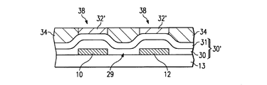
次に、図7を参照すると、別の実施例が示されており、その場合には、パッシベーション層34が導電層32と共に実質的に平坦状に形成されており、導電層32は導電性プレート10及び12の上に少なくとも部分的に設けられている。1実施例においては、誘電体層30を形成した後にパッシベーション層34を形成する。パッシベーション層34をパターン形成し且つエッチングして開口38を形成し、導電性プレート10及び12の全て又は少なくとも一部の上側に存在する誘電体層30の一部を露出させる。次いで、導電層32をパッシベーション層34の上に形成し、パターン形成し且つエッチングして実質的にパッシベーション層34と共に平坦状に開口38内に導電性領域32′を形成する。導電性領域32′は図7に示したように導電性プレート10及び12の少なくとも一部の上に存在しており且つ指先が層16の上表面と接触する場合の静電放電保護を与える。
【0039】
一方、導電性領域32′はパッシベーション層34を形成する前に形成し、次いで導電性プレート10及び12の上側における領域において誘電体層30の上側でパターン形成し且つエッチングすることが可能である。この実施例においては、次いで、パッシベーション層34を形成し且つエッチバックして図7に示したように導電性領域32′と共に実質的に平坦状とさせる。層の最適なパターン及び/又は所望の層の各々を形成するシーケンスは、セル3の感度を最大としながら、導電性プレート10,12ではなく導電層32又は導電性領域32′を介して静電荷を散逸させることによりセンサ回路を適切に損傷から保護するものである。
【0040】
以上、本発明の具体的実施の態様について詳細に説明したが、本発明は、これら具体例にのみ制限されるべきものではなく、本発明の技術的範囲を逸脱することなしに種々の変形が可能であることは勿論である。
【0041】
以下の関連特許出願の各々はあるタイプの静電放電保護方法及び装置を開示しており、それらの開示内容は引用によって本明細書に取込む。即ち、「容量型指紋検知アレイの静電放電保護(ELECTROSTATIC DISCHARGE PROTECTION OF A CAPACITIVE TYPE FINGERPRINT SENSING ARRAY)」という名称の1997年9月11日付で出願された米国特許出願第08/927,450号(エスティーマイクロエレクトロニクスドケット番号97−B−037)、「集積回路センサ用の選択的にドープした静電放電層(SELECTIVELY DOPED ELECTROSTATIC DISCHARGE LAYER FOR AN INTEGRATED CIRCUIT SENSOR)」という名称の1998年8月31日付で出願した米国特許出願第09/144,182号、「能動回路表面用の静電荷散逸(STATIC CHARGE DISSIPATIONFOR AN ACTIVE CIRCUIT SURFACE)」という名称の本願の基礎となっている米国特許出願と同日付で出願された米国特許出願(代理人ドケット番号119932−1042、エスティーマイクロエレクトロニクスドケット番号97−B−179)、「センサ用静電荷散逸パッド(STATIC CHARGE DISSIPATION PADS FOR SENSORS)」という題名の本願の基礎となっている米国特許出願と同日付で出願された米国特許出願(代理人ドケット番号119932−1038、エスティーマイクロエレクトロニクスドケット番号98−B−085)、「センサ導電層に接触させる装置及び方法(APPARATUS AND METHOD FOR CONTACTING A SENSOR CONDUCTIVE LAYER)」という題名の本願の基礎となっている米国特許出願と同日付で出願された米国特許出願(代理人ドケット番号119932−1039、エスティーマイクロエレクトロニクスドケット番号98−B−087)、「導電層に接触する装置及び方法(APPARATUS AND METHOD FOR CONTACTING A CONDUCTIVE LAYER)」という題名の本願の基礎となっている米国特許出願と同日付で出願された米国特許出願(代理人ドケット番号119932−1040、エスティーマイクロエレクトロニクスドケット番号98−B−088)、「センサ用の地形的静電保護グリッド(TOPOGRAPHICAL ELECTROSTATIC PROTECTION GRID FOR SENSORS)」という名称の本願出願の基礎となっている米国出願と同日付で出願された米国特許出願(代理人ドケット番号119932−1041、エスティーマイクロエレクトロニクスドケット番号98−B−090)の各々の開示内容を引用によって本明細書に取込む。
【図面の簡単な説明】
【図1】 本発明に基づくセンサアレイを示した概略ブロック図。
【図2】 本発明に基づく個別的なセンサセル及びそれらの電気的動作の物理的構造を示した概略図。
【図3】 本発明に基づく静電放電保護用の基本的構造の1実施例を示した概略断面図。
【図4】 本発明に基づく静電放電保護用の基本的構造の1実施例を示した概略断面図。
【図5】 本発明に基づく静電放電保護用の構造の別の実施例を示した概略断面図。
【図6】 本発明に基づく静電放電保護用の構造の更に説明の実施例を示した概略断面図。
【図7】 本発明に基づく静電放電保護用の構造の更に別の実施例を示した概略断面図。
【符号の説明】
1 ユーザ入力装置
2 アレイ
3 セル
4 水平方向スキャニングステージ
5 垂直方向スキャニングステージ
6 電源・スキャン制御装置
10,12 導電性プレート
16 絶縁層
18 増幅器
30,30′ 誘電体層
32 導電層
34 パッシベーション層
36 開口[0001]
BACKGROUND OF THE INVENTION
The present invention generally relates to the field of electrostatic charge dissipation, and more particularly, a structure (device) for protecting a sensor device from electrostatic discharge damage while maintaining sufficient sensitivity to collect sensor data. And a method.
[0002]
[Prior art]
Without limiting the scope of the present invention, as an example, the background will be described in connection with protecting an integrated circuit fingerprint sensor from the environment during normal use.
[0003]
Traditionally in this field, the detection of fingerprint patterns composed of lines or peaks and valleys is useful for identifying specific individuals based on the observation that each individual has a unique fingerprint. is there. Thus, fingerprints can be used not only to positively identify individuals, but also to exclude individuals with fingerprint shapes that do not match an existing set of patterns.
[0004]
Fingerprint detection has evolved from optical and mechanical detection techniques that collect fingerprint images. In these systems, mechanical and optical sensors typically take a fingerprint image using a scanner or camera, process it into an analog or digital signal that can be analyzed, and An output is provided based on the collected signal. However, the illumination and contrast conditions available when the image is acquired affects the analysis of the acquired data and thus the sensor output. Furthermore, the image acquisition system is easily fooled using false images. Furthermore, conventional optical sensors typically require large optical systems, making it unrealistic to make these types of sensors portable systems.
[0005]
Another type of fingerprint sensor is a capacitive sensor as disclosed by the inventor in US Pat. No. 4,353,056 to Tsikos. This patent uses a sensor incorporating a sensing member with a sensing surface for receiving a fingerprint. The detection surface comprises means for detecting peaks and valleys in the skin of the finger being observed. The detection member includes a number of capacitors for detecting a fingerprint pattern when the finger is pressed against the detection surface. Information obtained by the detection member is converted into an electrical signal. These capacitors are isolated from the environment of use by a flexible membrane that itself conforms to the shape of the fingerprint. However, repeated flexing and compression of the flexible membrane causes device failure and the need to replace the membrane.
[0006]
The inventor has described Ruell et al. U.S. Pat. No. 4,385,831 discloses a fingerprint sensor that provides an electrical output signal in response to fingerprint topography. The sensor incorporates a contact body or contact body formed at least in part by a light transmissive elastic material. The elastic contact material can be attached to a flat sensor plate having a light receiving surface. The sensor further incorporates a light source and photodetector for measuring the peaks and valleys of the fingerprint. The elastic nature of the contact body repeatedly compresses and bends, which degrades the contact point between the sensor and the finger.
[0007]
Current methods and structures to protect the sensor from the intended use environment are unique environmental conditions in which the sensor is exposed, particularly human skin or other objects that may be in contact with or in close proximity to the sensor. It has also been found not to address the problem of static buildup above. Sensor protection and sensitivity usually must be carefully balanced to achieve both an acceptable signal-to-noise ratio and adequate protection. In general, as sensor protection increases, sensor sensitivity decreases. The current electrostatic discharge circuit does not protect the sensor circuit from electrostatic discharge if electrical damage occurs in the active circuit or sensor surface structure that forms part of the sensor circuit during use.
[0008]
Since the sensor and user may be exposed to a variety of environmental conditions that can generate significantly different potentials compared to objects at different potentials, i.e. ground, the sensor has durable electrostatic discharge protection. It turns out that it should be. For example, if a user approaches a sensor with a significantly different voltage, a sudden electrical discharge may cause sensor malfunction, which is temporary or permanent. There is a case.
[0009]
Typical electrostatic discharge protection circuits for solid state arrays may have relatively poor performance. This is because, in this type of circuit configuration, the cell's buried and ungrounded capacitor plate is connected to the transistor gate and / or the cell's ungrounded and buried capacitor plate is reversed. This is because it is usually connected to the system ground potential by a biased diode. In this type of configuration and arrangement, the electrostatic charge carried by the human body and its fingertips can be in the range of several kilovolts (kV) or higher, and the dielectric / passivation on the top side of the solid state cell. May be high enough to break the layer. When such a breakdown occurs, the potential at the ungrounded circuit node associated with the embedded capacitor plate may increase and cause damage to the associated array cell. Damage to the data or sensor must be avoided while maintaining the sensitivity of the sensor near the optimum level.
[0010]
Another significant problem with current structures for protecting fingerprint sensors is contamination from substances such as oils and proteins present on the finger surface. In order to remove these contaminants, it is often necessary to use organic or inorganic solvents or detergents to clean the sensor surface. Therefore, electrostatic discharge protection must be durable against these often corrosive compounds.
[0011]
Another area of concern is hygiene. Fingers and the environment tend to contain a large number of microorganisms and bacteria, which are removed from the sensor along with other contaminants. Antibacterial and antibacterial disinfectants are often used to clean sensors to remove these microorganisms and bacteria and reduce the likelihood of infection among users. These disinfectants often have harsh abrasives, enzymes, organic or inorganic solvents or detergents. Thus, electrostatic discharge protection must be durable against these often corrosive cleaning compounds.
[0012]
[Problems to be solved by the invention]
There is a need for structures (apparatus) and methods that maintain sensor ability to withstand mechanical stresses and protect the sensor from electrostatic discharge. Such a structure not only allows the sensor to continue to function during normal use, but also withstands extreme conditions such as humidity, electricity, heat, light, etc. that the sensor may be exposed to. There must be. The electrostatic discharge structure of the sensor should be resistant to chemical detergents and solvents and compatible with the basic components of the sensor.
[0013]
Accordingly, the present invention has been made in view of the above points, and an object of the present invention is to provide a technique for solving the above-described drawbacks of the prior art and improving the electrostatic discharge protection characteristics of the sensor. Another object of the present invention is to provide a method and structure (apparatus) with improved protection against electrostatic discharge in sensors such as fingerprint sensors.
[0014]
[Means for Solving the Problems]
The present invention provides a method and system for providing electrostatic discharge capability in a sensor circuit such as a fingerprint sensor. In a type of sensor array in which the present invention is useful, each sensing cell has an ungrounded metal capacitor plate that is covered by a dielectric. For example, an ungrounded object such as a fingertip in contact with or in close proximity to the dielectric forms a third capacitor plate between the metal capacitor plates. The electrostatic charge carried by the human body may be high enough to destroy the dielectric layer covering the metal capacitor plate. The present invention improves the electrostatic discharge performance of such a sensor array.
[0015]
The present invention provides a process and apparatus for dissipating electrostatic charge, wherein a dielectric layer is disposed over first and second conductive capacitor plates, separating the first and second conductive plates. is doing. A conductive layer is disposed on at least a portion of the dielectric layer and disposed on or adjacent to a portion of the conductive plate. The present invention can also include a protective layer adjacent to or disposed on a portion of the conductive layer.
[0016]
DETAILED DESCRIPTION OF THE INVENTION
Various embodiments of the present invention are described in detail below for the manufacture and use of the invention, but the present invention provides a number of applicable inventive concepts that can be implemented in a variety of specific embodiments. Should be understood. The specific embodiments described herein are merely illustrative of ways to make and use the invention and do not delimit the scope of the invention.
[0017]
As background, referring to FIG. 1, a block diagram of a user input device 1 is shown. The user input device 1 is preferably integrated in a single chip and has an array 2 consisting of a plurality of sensors or pixel cells 3. For convenience of explanation, the array 2 is shown as having nine cells 3. In an actual apparatus, there is a high possibility that more than nine cells are provided. Each individual sensing cell 3 represents one pixel of the array 2 and is usually smaller than the width of the fingerprint crest. A sufficient number of cells 3 are provided in the array 2 so that it is possible to detect several peaks and valleys of the fingerprint. In the preferred embodiment, the pixel cells 3 are provided at a pitch of about 50 μm, which corresponds to a resolution of about 508 dots per inch (dpi) for a fingerprint image.
[0018]
The apparatus 1 has a horizontal scanning stage 4 and a vertical scanning stage 5. Scanning stages 4 and 5 make it possible to detect from one cell in the array 2 at a time according to a predetermined scanning pattern.
[0019]
The input sensor device 1 has a power supply and scan control device 6. The power supply and scan controller 6 supplies a reference voltage to each cell 3 of the array 2. The power supply and scan controller 6 further operates the scanning stages 4 and 5 to generate the desired scanning of the cell 3.
[0020]
For further background, referring to FIG. 2, the structure and operation of cell 3 is shown. A preferred cell of the present invention is disclosed in Tartagni US patent application Ser. No. 08 / 799,543, filed on Feb. 13, 1997, entitled “CAPACTIVE DISTANCE SENSOR”. The disclosure of which application is incorporated herein by reference. The technique of the present invention uses an active pixel configuration based on capacitive feedback sensing circuitry.
[0021]
Each cell 3 (3a, 3b) has a first
[0022]
Each cell 3 has a high gain inverting amplifier 18 (18a, 18b). The input of the amplifier 18 is input to a reference voltage source V via an input capacitor 20 (20a, 20b). ref Connected to. The output of each amplifier 18 is output V out (V outa , V outb ). The input of each amplifier 18 is connected to a respective
[0023]
When no object is present on the surface of the insulating
[0024]
The scanning stages 4 and 5 of FIG. 1 operate to allow a number of cells 3 in the array 2 to be read sequentially. The sensor 3 operates in two phases. During the first phase, the amplifier 18 is reset by the switch 28 (28a, 28b) by shorting the input and output of the amplifier 18. This causes the amplifier 18 to stabilize to its logical threshold. During the second phase, a fixed charge is input to the amplifier, causing the output voltage to swing inversely proportional to the feedback capacitance, which is the effective capacitance between the
[0025]
For a fixed amount of input charge, the output of amplifier 18 is in the range between the two limits depending on the effective feedback capacitance value. The first limit is the saturation voltage level when the effective feedback capacity is very small. The second limit is a voltage close to a logical threshold that is a reset value when the effective feedback capacity is large. Since the distance between the skin and the sensor changes the effective feedback capacity of the charge integrator, the output of the
[0026]
The structure and method of the present invention can be used with a variety of image sensors known to those skilled in the art in view of, for example, the fingerprint sensor described herein as an example and the present disclosure.
[0027]
As described above, when using the capacitive coupling sensor described above, it is possible to achieve a resolution of 508 dpi at the maximum. If the image processing algorithm is improved, it is possible to expect a sensor with a resolution of 750 dpi or higher. For use in detecting fingerprint peaks and valleys, a fingerprint pattern is sampled using an array 2 of cells. The overall chip can also include additional timing and voltage controls and references in addition to the controls and references described above.
[0028]
A structure and method for dissipating electrostatic charges and protecting pixel cells will now be described. With reference to FIG. 3, the case where the insulating
[0029]
In FIG. 3, a schematic cross-sectional view of the insulating
A
[0030]
The
[0031]
The thickness of the
[0032]
The selected conductive material has a sheet resistance that is low enough to allow the electrostatic charge to dissipate through this layer to prevent the electrostatic charge from reaching the
[0033]
As an example, in one embodiment in which the
[0034]
Referring now to FIG. 4, in the preferred embodiment, a photoresist (not shown) is formed and patterned to form
[0035]
Referring now to FIG. 5, another embodiment is shown, in which case the
[0036]
Referring now to FIG. 6, another embodiment is shown in which a
[0037]
In this embodiment in which a
[0038]
Referring now to FIG. 7, another embodiment is shown in which a
[0039]
On the other hand, the conductive region 32 'can be formed prior to forming the
[0040]
Although specific embodiments of the present invention have been described in detail above, the present invention should not be limited to these specific examples, and various modifications can be made without departing from the technical scope of the present invention. Of course, it is possible.
[0041]
Each of the following related patent applications discloses certain types of electrostatic discharge protection methods and apparatus, the disclosures of which are incorporated herein by reference. That is, US Patent Application No. 08 / 927,450 filed on Sep. 11, 1997, entitled “ELECTROSTATIC DISCHARGE PROTECTION OF A CAPACITIVE TYPE FINGERPRINT SENSING ARRAY”. EST Microelectronics Docket No. 97-B-037), August 31, 1998, entitled “SELECTIVELY DOPED ELECTROSTATIC DISCHARGE LAYER FOR AN INTEGRATED CIRCUIT SENSOR” No. 09 / 144,182 filed on date, “Static charge dissipation for active circuit surfaces (ST US patent applications filed on the same date as the US patent application on which this application is entitled "TIC CHARGE DISPIPATION FOR AN ACTIVE CIRCUIT SURFACE" (Attorney Docket No. 119932-1042, Estee Microelectronics Docket No. 97- B-179), a U.S. patent application filed on the same date as the U.S. patent application entitled "STATIC CHARGE DISPIPATION PADS FOR SENSORS", filed on the same date as that of the present patent application (attorney docket number 119932). -1038, Estee Microelectronics Docket No. 98-B-085), “Apparatus and Methods FO US patent application filed on the same date as the US patent application on which this application is entitled "R CONTACTING A SENSOR CONDUCTIVE LAYER" (Attorney Docket No. 199932-1039, Estee Microelectronics Docket No. 98-B) -087), a US patent application filed on the same date as the US patent application underlying this application entitled "Apparatus and Methods for CONTACTING A CONDUCTIVE LAYER" Docket No. 199932-1040, Estee Microelectronics Docket No. 98-B-088), “TOPOGRAPHIC ELECTROSTA US patent applications filed on the same date as the US application under this application entitled "TIC PROTECTION GRID FOR SENSORS" (Attorney Docket No. 11932-1041, Estee Microelectronics Docket No. 98-B-) 090), the disclosures of each of which are incorporated herein by reference.
[Brief description of the drawings]
FIG. 1 is a schematic block diagram showing a sensor array according to the present invention.
FIG. 2 is a schematic diagram illustrating the physical structure of individual sensor cells and their electrical operation according to the present invention.
FIG. 3 is a schematic sectional view showing one embodiment of a basic structure for electrostatic discharge protection according to the present invention.
FIG. 4 is a schematic sectional view showing one embodiment of a basic structure for electrostatic discharge protection according to the present invention.
FIG. 5 is a schematic sectional view showing another embodiment of the structure for electrostatic discharge protection according to the present invention.
FIG. 6 is a schematic sectional view showing an example of further explanation of the structure for electrostatic discharge protection according to the present invention.
FIG. 7 is a schematic sectional view showing still another embodiment of the structure for protecting electrostatic discharge according to the present invention.
[Explanation of symbols]
1 User input device
2 Array
3 cells
4 Horizontal scanning stage
5 Vertical scanning stage
6 Power supply / scan control device
10,12 Conductive plate
16 Insulation layer
18 Amplifier
30, 30 'dielectric layer
32 Conductive layer
34 Passivation layer
36 opening
Claims (7)
基板上に互いに離隔して形成されており且つ各々が指先等の接地されていない物体との間で検知すべき容量を画定する複数個のコンデンサを形成する複数個の導電性プレート、
前記複数個の導電性プレートを被覆しており且つその上表面は前記物体を接触させることが可能なセンサ表面を画定している絶縁層、
を有しており、
前記絶縁層が、
前記複数個の導電性プレートを被覆して前記基板上に形成されている誘電体層と、
前記誘電体層の少なくとも一部の上に形成されている静電放電保護用の導電層と、
前記導電層の少なくとも一部の上又は少なくとも前記誘電体層の上で前記導電層が形成されていない部分の上に形成した機械的保護用の硬質のパッシベーション層と、
を具備していることを特徴とする容量結合型センサ用集積回路。In the capacitively coupled sensor integrated circuit,
A plurality of conductive plates forming a plurality of capacitors, which are formed on the substrate apart from each other and each define a capacitance to be detected with an ungrounded object such as a fingertip;
An insulating layer covering the plurality of conductive plates and having an upper surface defining a sensor surface capable of contacting the object;
Have
The insulating layer is
A dielectric layer formed on the substrate to cover the plurality of conductive plates;
A conductive layer for electrostatic discharge protection formed on at least a portion of the dielectric layer;
A hard passivation layer for mechanical protection formed on at least a part of the conductive layer or at least on a portion of the dielectric layer where the conductive layer is not formed;
An integrated circuit for capacitively coupled sensors, comprising:
Applications Claiming Priority (2)
| Application Number | Priority Date | Filing Date | Title |
|---|---|---|---|
| US09/223,629 US6440814B1 (en) | 1998-12-30 | 1998-12-30 | Electrostatic discharge protection for sensors |
| US09/223629 | 1998-12-30 |
Publications (2)
| Publication Number | Publication Date |
|---|---|
| JP2000196026A JP2000196026A (en) | 2000-07-14 |
| JP4745477B2 true JP4745477B2 (en) | 2011-08-10 |
Family
ID=22837348
Family Applications (1)
| Application Number | Title | Priority Date | Filing Date |
|---|---|---|---|
| JP36093299A Expired - Lifetime JP4745477B2 (en) | 1998-12-30 | 1999-12-20 | Electrostatic discharge protection for sensors |
Country Status (4)
| Country | Link |
|---|---|
| US (2) | US6440814B1 (en) |
| EP (1) | EP1017010B1 (en) |
| JP (1) | JP4745477B2 (en) |
| DE (1) | DE69939365D1 (en) |
Families Citing this family (26)
| Publication number | Priority date | Publication date | Assignee | Title |
|---|---|---|---|---|
| US6091082A (en) * | 1998-02-17 | 2000-07-18 | Stmicroelectronics, Inc. | Electrostatic discharge protection for integrated circuit sensor passivation |
| DE60032286T8 (en) * | 1999-06-10 | 2007-09-27 | Nippon Telegraph And Telephone Corp. | Device for recognizing surface shapes |
| US6423995B1 (en) * | 1999-07-26 | 2002-07-23 | Stmicroelectronics, Inc. | Scratch protection for direct contact sensors |
| US6665428B1 (en) * | 2000-08-28 | 2003-12-16 | Stmicroelectronics, Inc. | Resistive finger detection for fingerprint sensor |
| US6873044B2 (en) * | 2000-09-11 | 2005-03-29 | Xytrans, Inc. | Microwave monolithic integrated circuit package |
| JP3887252B2 (en) * | 2002-03-15 | 2007-02-28 | 日本電信電話株式会社 | Manufacturing method of surface shape recognition sensor |
| TW540128B (en) * | 2002-07-12 | 2003-07-01 | Hannstar Display Corp | Manufacturing method of X-ray detector array |
| JP3741282B2 (en) * | 2003-07-28 | 2006-02-01 | セイコーエプソン株式会社 | INPUT DEVICE, ELECTRONIC DEVICE, AND DRIVE METHOD FOR INPUT DEVICE |
| JP4363281B2 (en) * | 2004-09-08 | 2009-11-11 | オムロン株式会社 | Capacity measuring device and method, and program |
| US20060166657A1 (en) * | 2005-01-25 | 2006-07-27 | Parag Patel | Remote caller ID projection device |
| US7884432B2 (en) * | 2005-03-22 | 2011-02-08 | Ametek, Inc. | Apparatus and methods for shielding integrated circuitry |
| JP5045028B2 (en) * | 2006-08-16 | 2012-10-10 | 富士通セミコンダクター株式会社 | Surface shape sensor and manufacturing method thereof |
| JP4833031B2 (en) * | 2006-11-06 | 2011-12-07 | 富士通セミコンダクター株式会社 | Surface shape sensor and manufacturing method thereof |
| US8124490B2 (en) | 2006-12-21 | 2012-02-28 | Stats Chippac, Ltd. | Semiconductor device and method of forming passive devices |
| WO2010121058A2 (en) | 2009-04-17 | 2010-10-21 | 3M Innovative Properties Company | Lightning protection sheet with patterned discriminator |
| US8383443B2 (en) | 2010-05-14 | 2013-02-26 | International Business Machines Corporation | Non-uniform gate dielectric charge for pixel sensor cells and methods of manufacturing |
| US20120092324A1 (en) | 2010-10-18 | 2012-04-19 | Qualcomm Mems Technologies, Inc. | Touch, handwriting and fingerprint sensor with elastomeric spacer layer |
| US9024910B2 (en) | 2012-04-23 | 2015-05-05 | Qualcomm Mems Technologies, Inc. | Touchscreen with bridged force-sensitive resistors |
| KR101698144B1 (en) * | 2013-07-11 | 2017-01-19 | 핑거프린트 카드즈 에이비 | Fingerprint sensing device with protective coating |
| EP3087349A4 (en) * | 2013-12-27 | 2017-08-30 | BYD Company Limited | Capacitance detecting device for fingerprint identification and fingerprint identification apparatus comprising the same |
| KR20160130747A (en) | 2013-12-30 | 2016-11-14 | 비와이디 컴퍼니 리미티드 | Sensor for detecting fingerprint and fingerprint identification appratus and controlling method of sensor for detecting fingerprint |
| TWI485821B (en) | 2014-02-24 | 2015-05-21 | Dynacard Co Ltd | Package module of fingerprint identification chip and method of the same |
| US9790085B1 (en) | 2016-06-16 | 2017-10-17 | Nxp Usa, Inc. | Actively preventing charge induced leakage of semiconductor devices |
| TWI584201B (en) * | 2016-07-17 | 2017-05-21 | 金佶科技股份有限公司 | Identification apparatus and identification method |
| TWI648861B (en) * | 2018-02-13 | 2019-01-21 | 富創微電子有限公司 | High-voltage capacitor structure and digital isolation device |
| US11710759B2 (en) * | 2019-12-23 | 2023-07-25 | Integrated Biometrics, Llc | Single contact relief print generator |
Family Cites Families (40)
| Publication number | Priority date | Publication date | Assignee | Title |
|---|---|---|---|---|
| US3921167A (en) | 1974-06-14 | 1975-11-18 | Ibm | Capacitive circuitboard |
| DE2508154C3 (en) | 1974-12-03 | 1978-06-15 | Pentel K.K., Tokio | Input plate |
| JPS586966B2 (en) | 1977-05-24 | 1983-02-07 | ぺんてる株式会社 | capacitive coupling tablet |
| US4290052A (en) | 1979-10-26 | 1981-09-15 | General Electric Company | Capacitive touch entry apparatus having high degree of personal safety |
| JPS56169368A (en) | 1980-05-30 | 1981-12-26 | Sharp Corp | High withstand voltage mos field effect semiconductor device |
| US4353056A (en) | 1980-06-05 | 1982-10-05 | Siemens Corporation | Capacitive fingerprint sensor |
| US4394773A (en) | 1980-07-21 | 1983-07-19 | Siemens Corporation | Fingerprint sensor |
| JP2702131B2 (en) * | 1987-06-12 | 1998-01-21 | キヤノン株式会社 | Image reading apparatus and image information reading apparatus having the same |
| US5331580A (en) * | 1989-01-31 | 1994-07-19 | Norand Corporation | Data capture system with communicating and recharging docking apparatus, and modular printer and hand-held data terminal means cooperable therewith |
| JPH0425200A (en) * | 1990-05-18 | 1992-01-28 | Fujitsu Ltd | Method of protecting mounted component against damage due to electrostatic discharge |
| GB2244164A (en) * | 1990-05-18 | 1991-11-20 | Philips Electronic Associated | Fingerprint sensing |
| JPH05136295A (en) * | 1991-11-12 | 1993-06-01 | Nec Ic Microcomput Syst Ltd | Semiconductor integrated circuit device |
| JPH0758234B2 (en) * | 1992-04-16 | 1995-06-21 | 株式会社エニックス | Semiconductor matrix type fine surface pressure distribution sensor |
| EP0574213B1 (en) | 1992-06-08 | 1999-03-24 | Synaptics, Inc. | Object position detector |
| WO1994005042A1 (en) | 1992-08-14 | 1994-03-03 | International Business Machines Corporation | Mos device having protection against electrostatic discharge |
| US5463388A (en) | 1993-01-29 | 1995-10-31 | At&T Ipm Corp. | Computer mouse or keyboard input device utilizing capacitive sensors |
| US5514612A (en) * | 1993-03-03 | 1996-05-07 | California Micro Devices, Inc. | Method of making a semiconductor device with integrated RC network and schottky diode |
| JPH07176713A (en) * | 1993-12-20 | 1995-07-14 | Nec Corp | Contact-type image sensor |
| JPH07288651A (en) * | 1994-04-20 | 1995-10-31 | Canon Inc | Semiconductor device and photoelectric converter |
| US5847690A (en) | 1995-10-24 | 1998-12-08 | Lucent Technologies Inc. | Integrated liquid crystal display and digitizer having a black matrix layer adapted for sensing screen touch location |
| US5907627A (en) | 1995-11-06 | 1999-05-25 | Dew Engineering And Development Limited | Contact imaging device |
| JP4024335B2 (en) * | 1996-01-26 | 2007-12-19 | ハリス コーポレイション | Integrated circuit device having an opening exposing die of integrated circuit and manufacturing method thereof |
| US5963679A (en) * | 1996-01-26 | 1999-10-05 | Harris Corporation | Electric field fingerprint sensor apparatus and related methods |
| US5956415A (en) * | 1996-01-26 | 1999-09-21 | Harris Corporation | Enhanced security fingerprint sensor package and related methods |
| EP0790479B1 (en) | 1996-02-14 | 2002-01-16 | STMicroelectronics S.r.l. | Capacitive distance sensor, particularly for acquiring fingerprints |
| US6114862A (en) | 1996-02-14 | 2000-09-05 | Stmicroelectronics, Inc. | Capacitive distance sensor |
| US5778089A (en) * | 1996-03-04 | 1998-07-07 | Dew Engineering And Development Limited | Driver circuit for a contact imaging array |
| JPH10297013A (en) * | 1997-04-22 | 1998-11-10 | Tdk Corp | Thermal head |
| US6088471A (en) * | 1997-05-16 | 2000-07-11 | Authentec, Inc. | Fingerprint sensor including an anisotropic dielectric coating and associated methods |
| US5940526A (en) | 1997-05-16 | 1999-08-17 | Harris Corporation | Electric field fingerprint sensor having enhanced features and related methods |
| US6483931B2 (en) * | 1997-09-11 | 2002-11-19 | Stmicroelectronics, Inc. | Electrostatic discharge protection of a capacitve type fingerprint sensing array |
| JP3102395B2 (en) * | 1997-11-27 | 2000-10-23 | 日本電気株式会社 | Fingerprint detection device |
| US6163313A (en) | 1997-12-12 | 2000-12-19 | Aroyan; James L. | Touch sensitive screen and method |
| US6091132A (en) * | 1997-12-19 | 2000-07-18 | Stmicroelectronics, Inc. | Passivation for integrated circuit sensors |
| US6091082A (en) * | 1998-02-17 | 2000-07-18 | Stmicroelectronics, Inc. | Electrostatic discharge protection for integrated circuit sensor passivation |
| JP3400347B2 (en) * | 1998-05-18 | 2003-04-28 | 日本電信電話株式会社 | Surface shape recognition sensor and method of manufacturing the same |
| JP3318865B2 (en) * | 1998-03-05 | 2002-08-26 | 日本電信電話株式会社 | Surface shape recognition sensor and method of manufacturing the same |
| TW396585B (en) * | 1998-06-06 | 2000-07-01 | United Microelectronics Corp | Electric static discharge protection circuit structure in dynamic random access memory and its manufacturing methods |
| RU2195048C2 (en) * | 1998-07-09 | 2002-12-20 | Инфинеон Текнолоджиз Аг | Semiconductor component with passivating layer |
| US6208009B1 (en) * | 1999-04-30 | 2001-03-27 | Digital Devices, Inc. | RC-networks in semiconductor devices and method therefor |
-
1998
- 1998-12-30 US US09/223,629 patent/US6440814B1/en not_active Expired - Lifetime
-
1999
- 1999-12-20 JP JP36093299A patent/JP4745477B2/en not_active Expired - Lifetime
- 1999-12-23 EP EP99310545A patent/EP1017010B1/en not_active Expired - Lifetime
- 1999-12-23 DE DE69939365T patent/DE69939365D1/en not_active Expired - Lifetime
-
2002
- 2002-07-01 US US10/186,801 patent/US6555888B2/en not_active Expired - Lifetime
Also Published As
| Publication number | Publication date |
|---|---|
| EP1017010A2 (en) | 2000-07-05 |
| US6555888B2 (en) | 2003-04-29 |
| EP1017010B1 (en) | 2008-08-20 |
| EP1017010A3 (en) | 2000-12-06 |
| JP2000196026A (en) | 2000-07-14 |
| US20020164862A1 (en) | 2002-11-07 |
| DE69939365D1 (en) | 2008-10-02 |
| US6440814B1 (en) | 2002-08-27 |
Similar Documents
| Publication | Publication Date | Title |
|---|---|---|
| JP4745477B2 (en) | Electrostatic discharge protection for sensors | |
| US6740945B2 (en) | Apparatus and method for contacting a conductive layer | |
| US6737329B2 (en) | Static charge dissipation pads for sensors | |
| US6686546B2 (en) | Static charge dissipation for an active circuit surface | |
| US6330145B1 (en) | Apparatus and method for contacting a sensor conductive layer | |
| US6326227B1 (en) | Topographical electrostatic protection grid for sensors | |
| US6180989B1 (en) | Selectively doped electrostatic discharge layer for an integrated circuit sensor | |
| JP4198239B2 (en) | Capacitive fingerprint sensing array electrostatic charge protection | |
| US7638350B2 (en) | Fingerprint sensors using membrane switch arrays | |
| US6518083B2 (en) | Surface shape recognition sensor and method of manufacturing the same | |
| US6091132A (en) | Passivation for integrated circuit sensors | |
| EP1308878A2 (en) | Capacitive sensor element for fingerprint sensor | |
| JPH11248665A (en) | Non-intrusive detection method for physical matter on detection surface by capacity type sensor | |
| US6429666B1 (en) | Capacitive circuit array for fingerprint sensing | |
| EP1408442A2 (en) | Fingerprint detector with improved sensing surface layer | |
| JP3516944B2 (en) | Surface shape recognition sensor and method of manufacturing the same | |
| JP3865367B2 (en) | Surface shape detector | |
| JP2003035507A (en) | Sensor for sensing surface shape and its manufacturing method |
Legal Events
| Date | Code | Title | Description |
|---|---|---|---|
| A621 | Written request for application examination |
Free format text: JAPANESE INTERMEDIATE CODE: A621 Effective date: 20061205 |
|
| A711 | Notification of change in applicant |
Free format text: JAPANESE INTERMEDIATE CODE: A711 Effective date: 20071010 |
|
| A977 | Report on retrieval |
Free format text: JAPANESE INTERMEDIATE CODE: A971007 Effective date: 20090826 |
|
| A131 | Notification of reasons for refusal |
Free format text: JAPANESE INTERMEDIATE CODE: A131 Effective date: 20100831 |
|
| A601 | Written request for extension of time |
Free format text: JAPANESE INTERMEDIATE CODE: A601 Effective date: 20101129 |
|
| A602 | Written permission of extension of time |
Free format text: JAPANESE INTERMEDIATE CODE: A602 Effective date: 20101202 |
|
| A601 | Written request for extension of time |
Free format text: JAPANESE INTERMEDIATE CODE: A601 Effective date: 20101222 |
|
| A602 | Written permission of extension of time |
Free format text: JAPANESE INTERMEDIATE CODE: A602 Effective date: 20101228 |
|
| A601 | Written request for extension of time |
Free format text: JAPANESE INTERMEDIATE CODE: A601 Effective date: 20110131 |
|
| A602 | Written permission of extension of time |
Free format text: JAPANESE INTERMEDIATE CODE: A602 Effective date: 20110203 |
|
| A521 | Request for written amendment filed |
Free format text: JAPANESE INTERMEDIATE CODE: A523 Effective date: 20110223 |
|
| TRDD | Decision of grant or rejection written | ||
| A01 | Written decision to grant a patent or to grant a registration (utility model) |
Free format text: JAPANESE INTERMEDIATE CODE: A01 Effective date: 20110412 |
|
| A61 | First payment of annual fees (during grant procedure) |
Free format text: JAPANESE INTERMEDIATE CODE: A61 Effective date: 20110512 |
|
| FPAY | Renewal fee payment (event date is renewal date of database) |
Free format text: PAYMENT UNTIL: 20140520 Year of fee payment: 3 |
|
| R150 | Certificate of patent or registration of utility model |
Ref document number: 4745477 Country of ref document: JP Free format text: JAPANESE INTERMEDIATE CODE: R150 Free format text: JAPANESE INTERMEDIATE CODE: R150 |
|
| S111 | Request for change of ownership or part of ownership |
Free format text: JAPANESE INTERMEDIATE CODE: R313113 |
|
| FPAY | Renewal fee payment (event date is renewal date of database) |
Free format text: PAYMENT UNTIL: 20140520 Year of fee payment: 3 |
|
| R350 | Written notification of registration of transfer |
Free format text: JAPANESE INTERMEDIATE CODE: R350 |
|
| R250 | Receipt of annual fees |
Free format text: JAPANESE INTERMEDIATE CODE: R250 |
|
| R250 | Receipt of annual fees |
Free format text: JAPANESE INTERMEDIATE CODE: R250 |
|
| S111 | Request for change of ownership or part of ownership |
Free format text: JAPANESE INTERMEDIATE CODE: R313113 |
|
| R350 | Written notification of registration of transfer |
Free format text: JAPANESE INTERMEDIATE CODE: R350 |
|
| R250 | Receipt of annual fees |
Free format text: JAPANESE INTERMEDIATE CODE: R250 |
|
| R250 | Receipt of annual fees |
Free format text: JAPANESE INTERMEDIATE CODE: R250 |
|
| R250 | Receipt of annual fees |
Free format text: JAPANESE INTERMEDIATE CODE: R250 |
|
| R250 | Receipt of annual fees |
Free format text: JAPANESE INTERMEDIATE CODE: R250 |
|
| EXPY | Cancellation because of completion of term |