JP4732897B2 - Power storage device and wiring pattern - Google Patents
Power storage device and wiring pattern Download PDFInfo
- Publication number
- JP4732897B2 JP4732897B2 JP2005513706A JP2005513706A JP4732897B2 JP 4732897 B2 JP4732897 B2 JP 4732897B2 JP 2005513706 A JP2005513706 A JP 2005513706A JP 2005513706 A JP2005513706 A JP 2005513706A JP 4732897 B2 JP4732897 B2 JP 4732897B2
- Authority
- JP
- Japan
- Prior art keywords
- double layer
- electric double
- parallel
- layer capacitor
- balance
- Prior art date
- Legal status (The legal status is an assumption and is not a legal conclusion. Google has not performed a legal analysis and makes no representation as to the accuracy of the status listed.)
- Active
Links
Images


Classifications
-
- H—ELECTRICITY
- H02—GENERATION; CONVERSION OR DISTRIBUTION OF ELECTRIC POWER
- H02J—CIRCUIT ARRANGEMENTS OR SYSTEMS FOR SUPPLYING OR DISTRIBUTING ELECTRIC POWER; SYSTEMS FOR STORING ELECTRIC ENERGY
- H02J7/00—Circuit arrangements for charging or depolarising batteries or for supplying loads from batteries
- H02J7/0013—Circuit arrangements for charging or depolarising batteries or for supplying loads from batteries acting upon several batteries simultaneously or sequentially
- H02J7/0014—Circuits for equalisation of charge between batteries
- H02J7/0016—Circuits for equalisation of charge between batteries using shunting, discharge or bypass circuits
-
- H—ELECTRICITY
- H01—ELECTRIC ELEMENTS
- H01L—SEMICONDUCTOR DEVICES NOT COVERED BY CLASS H10
- H01L27/00—Devices consisting of a plurality of semiconductor or other solid-state components formed in or on a common substrate
- H01L27/02—Devices consisting of a plurality of semiconductor or other solid-state components formed in or on a common substrate including semiconductor components specially adapted for rectifying, oscillating, amplifying or switching and having at least one potential-jump barrier or surface barrier; including integrated passive circuit elements with at least one potential-jump barrier or surface barrier
- H01L27/04—Devices consisting of a plurality of semiconductor or other solid-state components formed in or on a common substrate including semiconductor components specially adapted for rectifying, oscillating, amplifying or switching and having at least one potential-jump barrier or surface barrier; including integrated passive circuit elements with at least one potential-jump barrier or surface barrier the substrate being a semiconductor body
- H01L27/08—Devices consisting of a plurality of semiconductor or other solid-state components formed in or on a common substrate including semiconductor components specially adapted for rectifying, oscillating, amplifying or switching and having at least one potential-jump barrier or surface barrier; including integrated passive circuit elements with at least one potential-jump barrier or surface barrier the substrate being a semiconductor body including only semiconductor components of a single kind
- H01L27/0802—Resistors only
-
- H—ELECTRICITY
- H01—ELECTRIC ELEMENTS
- H01L—SEMICONDUCTOR DEVICES NOT COVERED BY CLASS H10
- H01L27/00—Devices consisting of a plurality of semiconductor or other solid-state components formed in or on a common substrate
- H01L27/02—Devices consisting of a plurality of semiconductor or other solid-state components formed in or on a common substrate including semiconductor components specially adapted for rectifying, oscillating, amplifying or switching and having at least one potential-jump barrier or surface barrier; including integrated passive circuit elements with at least one potential-jump barrier or surface barrier
- H01L27/04—Devices consisting of a plurality of semiconductor or other solid-state components formed in or on a common substrate including semiconductor components specially adapted for rectifying, oscillating, amplifying or switching and having at least one potential-jump barrier or surface barrier; including integrated passive circuit elements with at least one potential-jump barrier or surface barrier the substrate being a semiconductor body
- H01L27/08—Devices consisting of a plurality of semiconductor or other solid-state components formed in or on a common substrate including semiconductor components specially adapted for rectifying, oscillating, amplifying or switching and having at least one potential-jump barrier or surface barrier; including integrated passive circuit elements with at least one potential-jump barrier or surface barrier the substrate being a semiconductor body including only semiconductor components of a single kind
- H01L27/0805—Capacitors only
-
- Y—GENERAL TAGGING OF NEW TECHNOLOGICAL DEVELOPMENTS; GENERAL TAGGING OF CROSS-SECTIONAL TECHNOLOGIES SPANNING OVER SEVERAL SECTIONS OF THE IPC; TECHNICAL SUBJECTS COVERED BY FORMER USPC CROSS-REFERENCE ART COLLECTIONS [XRACs] AND DIGESTS
- Y02—TECHNOLOGIES OR APPLICATIONS FOR MITIGATION OR ADAPTATION AGAINST CLIMATE CHANGE
- Y02T—CLIMATE CHANGE MITIGATION TECHNOLOGIES RELATED TO TRANSPORTATION
- Y02T10/00—Road transport of goods or passengers
- Y02T10/60—Other road transportation technologies with climate change mitigation effect
- Y02T10/70—Energy storage systems for electromobility, e.g. batteries
Description
【技術分野】
【0001】
本発明は、電気二重層コンデンサを用いた蓄電装置の技術に関するものである。
【背景技術】
【0002】
近年、電気二重層コンデンサを利用した蓄電装置が、電気自動車等の動力源として有望視されている。電気二重層コンデンサは、比表面積が大きく、かつ、電気化学的に不活性な活性炭を電極として用い、この電極を電解質に浸し、電極と電解質との界面において生じる電気二重層に蓄積される電荷を利用するコンデンサである。
【0003】
電気二重層コンデンサは、耐電圧(定格電圧)が2〜3Vと低いため、蓄電装置は複数個の電気二重層コンデンサから構成されるのが一般的である。また、電気二重層コンデンサは、素子間で静電容量や内部抵抗等に大きなばらつきがあることが知られている。そのため、蓄電装置を複数の電気二重層コンデンサで構成した場合、すぐに満充電となるものや、なかなか満充電とならないものが発生し、各電気二重層コンデンサをバランスよく充電させることができないという問題がある。
【0004】
この問題を解決する技術として、「バランス回路方式」と呼ばれる技術が知られている。図6は、「バランス回路方式」を実現する回路の回路図を示している。図6に示す回路は、直列接続されたn(nは正数)個の電気二重層コンデンサC101〜C10n、及びn個のバランス抵抗R101〜R10nから構成される。バランス抵抗R101〜R10nは、各々、抵抗値が等しく、電気二重層コンデンサC101〜C10nに並列接続されている。これにより、各電気二重層コンデンサC101〜C10nに付与されるバイアス電圧は等しくなり、各電気二重層コンデンサをバランス良く充電させることができる。
【0005】
また、「バランス回路方式」を実現する他の回路として、非充電時にバランス抵抗を電気二重層コンデンサから電気的に切り離し、このコンデンサの両端電圧が所定値以上になったときに、該コンデンサとバランス抵抗とを並列接続するようにして、非充電時の放電を防止し、長期間電気エネルギを蓄積することができる回路が知られている(特許文献1)。
【0006】
さらに、「バランス回路方式」を実現する他の回路として、電気二重層コンデンサの両端子間の電圧と充電基準電圧とを比較する比較回路と、比較回路からの出力を受けて電気二重層コンデンサに対する充電電流をバイパスさせるバイパス回路とを備え、充電基準電圧の大きさを用途に応じて適宜切り替え、電気二重層コンデンサのバイアス電圧を調節することができる回路が知られている(特許文献2)。
【特許文献1】
実開平5−23527号公報
【特許文献2】
特開平6−343225号公報
【発明の開示】
【発明が解決しようとする課題】
【0007】
しかしながら、図6に示す回路、特許文献1、及び特許文献2記載の発明は、いずれも、電気二重層コンデンサに対して、並列接続されるバランス抵抗は1個であるため、バランス抵抗の抵抗値のばらつきにより、電気二重層コンデンサを均一に充電することができないという問題がある。
【0008】
また、バランス抵抗が破損してオープンとなると電気二重層コンデンサに付与されるバイアス電圧は大きく上昇し、各電気二重層コンデンサに付与されるバイアス電圧のバランスがくずれ、各電気二重層コンデンサをバランスよく充電することができなくなるという問題が発生する。また、バイアス電圧が電気二重層コンデンサの定格電圧を超えてしまい電気二重層コンデンサを破損させるという問題も発生する。
【0009】
本発明の目的は、電気二重層コンデンサをバランスよく充電させることができると共に、電気二重層コンデンサの破損を防止することができる蓄電装置を提供することである。
【課題を解決するための手段】
【0010】
本発明にかかる蓄電装置は、直列接続された複数の電気二重層コンデンサと、抵抗値が等しいm(mは4以上の整数)個のチップタイプの抵抗が並列接続されて回路基板上に配設されたバランス抵抗部とを備え、前記電気二重層コンデンサの各々に前記バランス抵抗部を並列接続し、前記直列接続する電気二重層コンデンサの個数を、ある1つの電気二重層コンデンサに並列接続された前記バランス抵抗部を構成する抵抗の1つがオープンになったとき、当該電気二重層コンデンサに付与される満充電のバイアス電圧が前記電気二重層コンデンサの定格電圧を越えない個数にし、当該電気二重層コンデンサに並列接続された前記バランス抵抗部を構成する抵抗の2つがオープンになったとき、前記バイアス電圧が前記定格電圧を超える個数にしたことを特徴とするものである。
【0011】
この構成によれば、直列接続された複数の電気二重層コンデンサの各々に対して、抵抗値を同一とするm(mは4以上の整数)個の抵抗が並列接続されたバランス抵抗部が並列接続されているため、バランス抵抗部の抵抗値のばらつきが抑制され、各電気二重層コンデンサを均一に充電することができる。また、バランス抵抗部を構成する抵抗の一部が破損して開放状態となっても、他に並列接続された抵抗の存在により、当該電気二重層コンデンサに付与されるバイアス電圧の上昇が抑制され、電気二重層コンデンサの破損を防止することができる。そのため、蓄電装置の信頼性が高まり、蓄電装置が接続される装置全体が機能しなくなるというような事態を回避することができる。さらに、いずれかの抵抗が破損したとしても、各電気二重層コンデンサに付与されるバイアス電圧のバランスが保たれ、蓄電装置を正常に機能させることができる。
また、この構成によれば、各電気二重層コンデンサに付与されるバイアス電圧が、定格電圧よりも小さくなるため、電気二重層コンデンサの破損を防止することができる。
【0012】
また、前記バランス抵抗部の抵抗値は、前記バランス抵抗部を構成する個々の抵抗の抵抗値の1/4以下であることが好ましい。
【0013】
この構成によれば、バランス抵抗部の抵抗値が、前記バランス抵抗部を構成する個々の抵抗の抵抗値の1/4以下、すなわち、バランス抵抗部を構成する抵抗の数が4個以上とされているため、例えばバランス抵抗部を構成するいずれか1個の抵抗が破損してオープンになったとしても、バランス抵抗部の抵抗値の上昇率を25%以下に抑制することができ、それに伴ってバイアス電圧の上昇率も25%以下に抑制することができる。そのため、バイアス電圧の値を、電気二重層コンデンサの定格電圧に対して25%以下に設定しておけば、抵抗が破損してオープンになったとしてもバイアス電圧の値が定格電圧を超える可能性を低くすることができ、電気二重層コンデンサの寿命を長くすることができる。
【0014】
また、前記バランス抵抗部の抵抗値は、前記バランス抵抗部を構成する個々の抵抗の抵抗値の1/6以上であることが好ましい。
【0015】
この構成によれば、バランス抵抗部の抵抗値が、個々の抵抗の抵抗値の1/6以上、すなわち、バランス抵抗部の抵抗の数が、6個以下とされているため、抵抗の破損に起因するバイアス電圧の上昇を抑制しつつ、抵抗の数の増大に伴う電力損失が低下され、電気二重層コンデンサに蓄積された電荷の放電を抑制することができる。
【0016】
また、前記バランス抵抗部の抵抗値は、個々の抵抗の抵抗値の1/6以上、1/4以下であることが好ましい。
【0017】
この構成によれば、電気二重層コンデンサの超寿命化を図りつつ、電気二重層コンデンサに蓄積された電荷の放電を抑制することができる。
【0018】
また、前記バランス抵抗部の抵抗値を10Ω以上、500Ω以下としたことが好ましい。
【0019】
この構成によれば、充放電時における電気二重層コンデンサの損失を低下することができる。
【0020】
また、直列接続する電気二重層コンデンサの個数を、各電気二重層コンデンサに付与されるバイアス電圧が、電気二重層コンデンサの定格電圧よりも小さくなるような個数にしたことが好ましい。
【0021】
この構成によれば、各電気二重層コンデンサに付与されるバイアス電圧が、定格電圧よりも小さくなるため、電気二重層コンデンサの破損を防止することができる。
【0022】
また、前記バランス抵抗部に対して、更に、1又は複数の電気二重層コンデンサを並列接続させたことが好ましい。
【0023】
この構成によれば、バランス抵抗部に対して、更に1又は複数の電気二重層コンデンサを接続させる、すなわち、並列接続された電気二重層コンデンサを直列接続させるというように電気二重層コンデンサがマトリックス状に接続されるため、高耐久性、かつ、高容量の蓄電装置を提供することができる。
【0024】
本発明にかかる配線パターンは、電気二重層コンデンサを回路基板に複数個並列に接続するための配線パターンであって、前記配線パターンは、所定の間隔を設けて配列された3本以上の配線パターンを含み、隣接する配線パターン間に複数の電気二重層コンデンサが並列接続されると共に、前記配線パターン間に接続された隣接する2つの電気二重層コンデンサ間に抵抗値が等しいm個(mは4以上の整数)のチップタイプの抵抗を前記電気二重層コンデンサと並列接続させ、前記回路基板上に配設させ、前記電気二重層コンデンサは更に直列接続され、前記直列接続する電気二重層コンデンサの個数を、ある1つの電気二重層コンデンサに並列接続された前記バランス抵抗部を構成する抵抗の1つがオープンになったとき、当該電気二重層コンデンサに付与される満充電のバイアス電圧が前記電気二重層コンデンサの定格電圧を越えない個数にし、当該電気二重層コンデンサに並列接続された前記バランス抵抗部を構成する抵抗の2つがオープンになったとき、前記バイアス電圧が前記定格電圧を超える個数にしたことを特徴とするものである。
【0025】
この構成によれば、長手方向が平行となるように3本以上配列された配線パターンに対し、隣接する配線パターン間に並列接続された複数の電気二重層コンデンサのうち、隣接する2個の電気二重層コンデンサ間に複数の抵抗が、電気二重層コンデンサと並列接続されているため、配線パターンの全長を短くすることができる。そのため、配線抵抗が低下し、電気二重層コンデンサの充放電効率を向上させることができる。
【0026】
また、平行に配列された複数の配線パターン間に複数の抵抗及び複数の電気二重層コンデンサが電気的に接続されているため、抵抗が破損したとしても、他に並列接続されている抵抗の存在により、電気二重層コンデンサに付与されるバイアス電圧の上昇が抑制され、電気二重層コンデンサの破損を防止することができる。
また、この構成によれば、各電気二重層コンデンサに付与されるバイアス電圧が、定格電圧よりも小さくなるため、電気二重層コンデンサの破損を防止することができる。
【0027】
また、前記抵抗は、前記配線パターンの一方の配線面から接続され、前記電気二重層コンデンサは、前記配線パターンの他方の配線面から接続されることが好ましい。
【0028】
この構成によれば、配線パターンの一方の配線面に電気二重層コンデンサが接続され、配線パターンの他方の配線面に抵抗が接続されているため、電気二重層コンデンサと抵抗との両素子を配線パターンの一方面側のみから接続した場合に比して、配線パターンの全長を短くすることができる。そのため、配線抵抗が低下し、電気二重層コンデンサの充放電効率を向上させることができる。
【発明を実施するための最良の形態】
【0029】
以下、本発明の実施の形態を、図面を参照しながら説明する。
(実施の形態1)
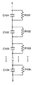
図1に本発明の実施の形態1による蓄電装置の回路図を示す。図1に示すように、本蓄電装置は、n(nは2以上の整数)個の電気二重層コンデンサC1〜Cn及びn個のバランス抵抗部R1〜Rnを備えている。以下、「電気二重層コンデンサ」のことを「コンデンサ」と略して表す。コンデンサC1〜Cnは直列接続されている。バランス抵抗部R1〜Rnは、それぞれ、コンデンサC1〜Cnに並列接続されている。
【0030】
バランス抵抗部R1〜Rnは同一構成であるため、バランス抵抗部R1のみ説明する。バランス抵抗部R1は、並列接続された5個の抵抗R11〜R15を備える。抵抗R11〜R15の各々の抵抗値は等しい。また、抵抗R11〜R15としては、チップタイプやリード線タイプのものを用いることができるが、特にこれに限定されるものではない。
【0031】
コンデンサC1〜Cnは同一構成であるため、コンデンサC1のみ説明する。コンデンサC1は、以下のように形成されたものである。外部引き出しリード線が取り付けられた厚さ20〜50μmのエッチングされたアルミニウム箔の上面に、活性炭粉末に所望の結合剤及び導電剤を混合した混合粉末からなるペーストを塗布して導電層を形成する。この導電層の上に、活性炭を主成分とする活性炭素層の分極電極を形成して一対の電気二重層電極を構成する。この電気二重層電極をセパレータを介して対面させて巻き回しコンデンサ素子を形成する。そして、このコンデンサ素子に電解液を含浸させ、アルミニウムケースに挿入し、開口部をシールする。
【0032】
電気二重層コンデンサの耐電圧は、その電解液の種類により定まり、この耐電圧により電気二重層コンデンサの定格電圧が決定される。通常1個の電気二重層コンデンサの定格電圧は2〜3Vの範囲である。
【0033】
図1に示すコンデンサC1〜Cn間に直流電圧Vを加え、各コンデンサを充電すると、各コンデンサC1〜Cnには、抵抗値の等しいバランス抵抗部R1〜Rnが並列接続されているため、直流電圧Vをコンデンサの個数で割ったバイアス電圧(V/n)が付与される。
【0034】
ここで、定格電圧2.6V、かつ、静電容量100FのコンデンサCiを6個直列接続し、抵抗Ri1〜Ri5の抵抗値を100Ωとし、コンデンサC1〜C6の両端に12Vの直流電圧を付与してコンデンサC1〜C6を充電する場合を考える。なお、バランス抵抗部Riの抵抗値は、抵抗Ri1〜Ri5の抵抗値が100Ωであるため、100を5で除した20Ωとなる。
【0035】
この場合、各コンデンサC1〜C6のバイアス電圧は、12Vを6で除した2.0Vとなる。この値はコンデンサC1〜C6の定格電圧である2.6Vよりも低いため、コンデンサC1〜C6の破損を防止することができる。従って、直列接続するコンデンサの数nは、直列接続されたコンデンサの両端に付与される直流電圧をV、各コンデンサの定格電圧をVTとすると、n>V/VTとすることが好ましい。
【0036】
次に、本蓄電装置と従来の蓄電装置との間で、バランス抵抗が破損したときのバイアス電圧の変化を比較する。バランス抵抗が1個である従来の蓄電装置では、抵抗が破損してオープンとなると、本蓄電装置のように並列接続された抵抗が存在していないため、コンデンサに付与されるバイアス電圧は大きく上昇し、直列接続されたコンデンサをバランスよく充電することができなくなる。また、バイアス電圧がコンデンサの定格電圧を超え、コンデンサを破損させる虞がある。
【0037】
一方、本蓄電装置では、バランス抵抗部R1の抵抗R11が破損してオープンとなっても、4個の抵抗R12〜R15が存在する。そのため、コンデンサC1の定格電圧である2.6Vを超えず、コンデンサC1の破損を防止することができる。
【0038】
次に、バランス抵抗部Riを構成する抵抗の好ましい数について説明する。図2は、バランス抵抗部Riを構成する抵抗の数を3個としたときの蓄電装置の回路図を示している。抵抗Ri1〜Ri3の抵抗値はrである。コンデンサC1〜C6の定格電圧は2.6Vである。コンデンサC1〜C6の両端には、12Vの電圧が付与されている。
【0039】
図2に示す蓄電装置で、抵抗R11が破損した場合を考える。この場合、バランス抵抗部R1は、2個の抵抗R12,R13が並列接続された回路となるため、その抵抗値は、r/2となる。一方、抵抗R11が破損する前は、バランス抵抗部R1の抵抗値は、r/3である。従って、抵抗R11の破損後のバランス抵抗部R1の抵抗値は、破損前に比して(r/2)/(r/3)=1.5倍となり、50%アップする。それに伴って、バイアス電圧もコンデンサC1の定格電圧である2.6Vを超えてしまう。
【0040】
図3は、図2の蓄電装置に対して、バランス抵抗部Riを構成する抵抗の数を7個としたときの回路図を示している。図3に示す蓄電装置において抵抗R11が破損すると、バランス抵抗部Riの抵抗値は、r/6となり、破損前に対し、(r/6)/(r/7)=7/6倍となり、バイアス電圧の上昇は、図2に示す蓄電装置に比べて小さくなる。したがって、抵抗の破損によるバイアス電圧の上昇を抑制させるという観点からは、バランス抵抗部Riを構成する抵抗の数を増やすことが好ましい。
【0041】
しかしながら、そうすると、抵抗の数が増えることに起因して、電力損失が増大し、充電された電荷が、充電後直ちに放電されてしまう。従って、バランス抵抗部Riを構成する抵抗の個数としては、4〜6個が好ましく、より好ましくは5個である。つまり、バランス抵抗部Riの抵抗値は、バランス抵抗部Riを構成する個々の抵抗の抵抗値の1/6以上、1/4以下にすることが好ましく、より好ましくは、1/5である。
【0042】
以上説明したように、実施の形態1による蓄電装置によれば、バランス抵抗部R1〜Rnは、各々、並列接続された複数の抵抗Ri1〜Ri5から構成されているため、バランス抵抗部R1〜Rnの抵抗値のばらつきを抑制することができ、コンデンサC1〜Cnを均一に充電することができる。
【0043】
また、バランス抵抗部Riを並列接続された複数の抵抗から構成したため、いずれかの抵抗が破損してオープンになったとしても、残りの並列接続された抵抗の存在により、バイアス電圧の上昇が抑制され、各コンデンサC1〜Cnをバランスよく充電することができることに加え、コンデンサの破損を防止することができる。
【0044】
なお、前記バランス抵抗部の抵抗値は、コンデンサC1〜Cnの充放電時の損失を低下させるという観点からは、10〜500Ωの範囲好ましい。
【0045】
(実施の形態2)
図4は本発明の実施の形態2による蓄電装置の回路図を示している。実施の形態2による蓄電装置は、実施の形態1による蓄電装置に対し、コンデンサを並列接続させたものである。具体的には、図4に示す蓄電装置は、直列接続されたn個のセル群CL1〜CLn、及び各セル群CL1〜CLnに対して並列接続されたn個のバランス抵抗部R1〜Rnを備えている。i(i=1,2,3,・・・n)番目のセル群CLiには、4個のコンデンサCi1〜Ci4が並列接続されている。また、バランス抵抗部R1〜Rnは、図1に示す実施の形態1の蓄電装置と同一構成であるため、説明を省略する。
【0046】
このようにコンデンサを並列接続して、蓄電装置の容量を増大させても、セル群CL1〜CLnにはバランス抵抗部R1〜Rnが並列接続されているため、バランス抵抗部R1〜Rnの抵抗値のばらつきが抑制され、コンデンサCi1〜Ci4を均一に充電することができる。
【0047】
また、バランス抵抗部Riを構成する抵抗Ri1〜Ri5のうち、いずれかの抵抗が破損してオープンになったとしても、残りの並列接続された抵抗の存在により、セル群CLiに対するバイアス電圧の上昇が抑制され、セル群CL1〜CLnの各々にバランスよくバイアス電圧を付与することができ、コンデンサC11〜Cn5の破損を防止することができる。
【0048】
さらに、電気二重層コンデンサを4個並列に接続しているので、静電容量を高めることができ、例えば、大容量・大電流を必要とする電気自動車などの各制御用電源或いは補助電源として本蓄電装置を使用することができる。なお、図4では、セル群CLiを構成するコンデンサの数を4個としたが、これに限定されず、2個、3個、或いは5個以上としてもよい。
【0049】
次に、蓄電装置の構造について説明する。図5は、図4に示す蓄電装置において、セル群CL1〜CLnの数を7個とした場合の構造を示した図面である。図5に示すように、本蓄電装置は、8本の配線パターン1〜8がプリントされた回路基板10、4行7列のマトリックス状に配列された28個のコンデンサC11〜C74、及び35個の抵抗R11〜R75を備えている。
【0050】
配線パターン1〜8は、銅や銀等の導電体から構成され、細長い形状を有し、長手方向が平行となるように、一定の間隔を設けて回路基板10上に形成されている。ここで、配線パターン1〜8の間隔は、コンデンサC11〜C74の配置ピッチ程度である。
【0051】
配線パターン1及び8は、各々、長手方向に沿って4個の凸部11〜14が一定の間隔で形成されている。また、配線パターン2〜7には、長手方向の一方の一辺に沿って4個の凸部11〜14が一定の間隔で形成され、長手方向の他方の一辺に沿って4個の凸部11〜14が一定の間隔で形成されている。ここで、凸部11〜14の間隔は、コンデンサC11〜C74の配置ピッチ程度である。また、凸部11〜14には、コンデンサのリード線が差し込まれるスルーホールが形成されている。スルーホールの内壁にも導電体が形成されている。
【0052】
また、凸部11及び12間には、5個の抵抗を接続するためのT字状の端子20が、配線パターン1〜8の長手方向と直交する方向に突出するように形成されている。そして、配線パターン1〜8は、凸部11〜14及び端子20が対向するように形成されている。
【0053】
配線パターン1の端子20及び配線パターン2の端子20間には5個の抵抗R11〜R15が接続されている。同様にして、他の隣接する配線パターン間にも、端子20を介して5個の抵抗が接続されている。これにより、抵抗R11〜R15が並列接続される。他の抵抗も同様に並列接続される。
【0054】
配線パターン1及び2間には抵抗が接続される回路基板10の面とは反対側の面(裏面)からコンデンサC11〜C14が接続され、配線パターン2及び3間にはコンデンサC21〜C24が接続され、・・・、配線パターン7及び8間にはコンデンサC71〜C74が接続されている。詳細には、コンデンサCij(i=1〜7の整数、j=1〜4の整数、)は、一方のリード線が第j番目の配線パターンjの凸部11のスルーホールに差し込まれて半田付けされ、他方のリード線が配線パターンj+1の凸部11のスルーホールに差し込まれて半田付けされている。
【0055】
これにより、コンデンサC11〜C14は並列接続される。他のコンデンサも同様に並列接続される。
【0056】
このように、長手方向が平行となるように配線パターン1〜8を平行に配設し、隣接する配線パターン間に複数のコンデンサを並列接続させ、並列接続された2個のコンデンサ間に端子部20を形成し、この端子部20に5個の抵抗を接続すると共に、隣接する配線パターン間に裏面から4個のコンデンサを接続したため、配線パターンの全長を短くすることができる。そのため、配線抵抗が小さくなり、コンデンサC11〜C74の充電効率を向上させることができることに加え、回路基板10の小型化を図ることができる。
【0057】
なお、図5では、端子20は、凸部11及び12間に形成されているが、これに限定されず、他の凸部間に形成してもよい。また、配線パターン1〜8としては、回路基板10上にプリントされたものを用いたが、これに限定されず、導電性の部材から構成される平板状の部材を採用してもよい。
【産業上の利用可能性】
【0058】
本発明によれば、各電気二重層コンデンサをバランスよく充電することができ、かつ、電気二重層コンデンサの破損を防止しうる蓄電装置を提供することができる。
【図面の簡単な説明】
【0059】
【図1】本発明の実施の形態1による蓄電装置の回路図を示す。
【図2】バランス抵抗部を構成する抵抗の数を3個としたときの蓄電装置の回路図を示している。
【図3】図2の蓄電装置に対して、バランス抵抗部を構成する抵抗の数を7個としたときの回路図を示している。
【図4】本発明の実施の形態2による蓄電装置の回路図を示している。
【図5】図4に示す蓄電装置において、セル群CL1〜CLnの数を7個とした場合の構造を示した図面である。
【図6】従来の蓄電装置の回路図を示している。
【符号の説明】
【0061】
1〜8 配線パターン
10 回路基板
11〜14 凸部
20 端子
C1〜Cn コンデンサ
CL1〜CLn セル群
R1〜Rn バランス抵抗部【Technical field】
[0001]
The present invention relates to a technology of a power storage device using an electric double layer capacitor.
[Background]
[0002]
In recent years, power storage devices using electric double layer capacitors have been promising as power sources for electric vehicles and the like. An electric double layer capacitor uses activated carbon that has a large specific surface area and is electrochemically inactive as an electrode. The electrode is immersed in an electrolyte, and charges accumulated in the electric double layer generated at the interface between the electrode and the electrolyte are accumulated. This is the capacitor to use.
[0003]
Since the electric double layer capacitor has a low withstand voltage (rated voltage) of 2 to 3 V, the power storage device is generally composed of a plurality of electric double layer capacitors. In addition, it is known that electric double layer capacitors have large variations in capacitance, internal resistance and the like between elements. For this reason, when the power storage device is configured with a plurality of electric double layer capacitors, there is a problem that some of the electric double layer capacitors cannot be charged in a well-balanced state due to the occurrence of those that are immediately fully charged or those that do not readily fully charge. There is.
[0004]
As a technique for solving this problem, a technique called “balance circuit system” is known. FIG. 6 shows a circuit diagram of a circuit that realizes the “balance circuit system”. The circuit shown in FIG. 6 includes n (n is a positive number) electric double layer capacitors C101 to C10n connected in series and n balance resistors R101 to R10n. The balance resistors R101 to R10n have the same resistance value and are connected in parallel to the electric double layer capacitors C101 to C10n. As a result, the bias voltages applied to the electric double layer capacitors C101 to C10n are equal, and the electric double layer capacitors can be charged with a good balance.
[0005]
In addition, as another circuit for realizing the “balance circuit system”, the balance resistor is electrically disconnected from the electric double layer capacitor at the time of non-charging, and when the voltage across the capacitor exceeds a predetermined value, the capacitor and the balance are balanced. A circuit is known in which a resistor is connected in parallel to prevent discharge during non-charging and electric energy can be accumulated for a long period of time (Patent Document 1).
[0006]
Furthermore, as another circuit that realizes the “balance circuit system”, a comparison circuit that compares the voltage between both terminals of the electric double layer capacitor and the charging reference voltage, and an output from the comparison circuit that receives the output from the comparison circuit There is known a circuit that includes a bypass circuit that bypasses the charging current and that can appropriately switch the magnitude of the charging reference voltage according to the application and adjust the bias voltage of the electric double layer capacitor (Patent Document 2).
[Patent Document 1]
Japanese Utility Model Publication No. 5-23527 [Patent Document 2]
JP-A-6-343225 [Disclosure of the Invention]
[Problems to be solved by the invention]
[0007]
However, since the circuit shown in FIG. 6 and the inventions described in
[0008]
In addition, if the balance resistor is broken and becomes open, the bias voltage applied to the electric double layer capacitor greatly increases, the balance of the bias voltage applied to each electric double layer capacitor is lost, and each electric double layer capacitor is balanced. The problem that it becomes impossible to charge occurs. In addition, there is a problem that the bias voltage exceeds the rated voltage of the electric double layer capacitor and damages the electric double layer capacitor.
[0009]
An object of the present invention is to provide a power storage device that can charge an electric double layer capacitor in a well-balanced manner and can prevent the electric double layer capacitor from being damaged.
[Means for Solving the Problems]
[0010]
A power storage device according to the present invention includes a plurality of electric double layer capacitors connected in series and m (m is an integer of 4 or more) chip-type resistors having the same resistance value connected in parallel and arranged on a circuit board. The balance resistor portion is connected in parallel to each of the electric double layer capacitors, and the number of the electric double layer capacitors connected in series is connected in parallel to one electric double layer capacitor. When one of the resistors constituting the balance resistor section is opened, the number of the fully charged bias voltage applied to the electric double layer capacitor does not exceed the rated voltage of the electric double layer capacitor. When two of the resistors constituting the balance resistor unit connected in parallel to a capacitor are opened, the bias voltage exceeds the rated voltage. It is characterized in that the.
[0011]
According to this configuration, for each of the plurality of electric double layer capacitors connected in series, a balance resistor unit in which m resistors (m is an integer of 4 or more) having the same resistance value are connected in parallel is provided in parallel. Since they are connected, variation in the resistance value of the balance resistor portion is suppressed, and each electric double layer capacitor can be charged uniformly. In addition, even if a part of the resistor constituting the balance resistor part is broken and opened, the presence of another resistor connected in parallel suppresses an increase in the bias voltage applied to the electric double layer capacitor. The electric double layer capacitor can be prevented from being damaged. Therefore, it is possible to avoid a situation in which the reliability of the power storage device is increased and the entire device to which the power storage device is connected fails. Furthermore, even if one of the resistors is damaged, the balance of the bias voltage applied to each electric double layer capacitor is maintained, and the power storage device can function normally.
Further, according to this configuration, since the bias voltage applied to each electric double layer capacitor is smaller than the rated voltage, the electric double layer capacitor can be prevented from being damaged.
[0012]
Moreover, it is preferable that the resistance value of the said balance resistance part is 1/4 or less of the resistance value of each resistance which comprises the said balance resistance part.
[0013]
According to this configuration, the resistance value of the balance resistor portion is ¼ or less of the resistance value of each resistor constituting the balance resistor portion, that is, the number of resistors constituting the balance resistor portion is four or more. Therefore, even if any one of the resistors constituting the balance resistor portion is damaged and opened, for example, the rate of increase in the resistance value of the balance resistor portion can be suppressed to 25% or less, and accordingly Thus, the increase rate of the bias voltage can be suppressed to 25% or less. Therefore, if the bias voltage value is set to 25% or less of the rated voltage of the electric double layer capacitor, the bias voltage value may exceed the rated voltage even if the resistor breaks and opens. And the life of the electric double layer capacitor can be extended.
[0014]
Moreover, it is preferable that the resistance value of the said balance resistance part is 1/6 or more of the resistance value of each resistance which comprises the said balance resistance part.
[0015]
According to this configuration, the resistance value of the balance resistance unit is 1/6 or more of the resistance value of each resistor, that is, the number of resistances of the balance resistance unit is 6 or less. While suppressing an increase in the bias voltage due to this, power loss accompanying an increase in the number of resistors is reduced, and discharge of electric charges accumulated in the electric double layer capacitor can be suppressed.
[0016]
Moreover, it is preferable that the resistance value of the said balance resistance part is 1/6 or more and 1/4 or less of the resistance value of each resistance.
[0017]
According to this configuration, it is possible to suppress the discharge of the electric charge accumulated in the electric double layer capacitor while extending the life of the electric double layer capacitor.
[0018]
Moreover, it is preferable that the resistance value of the balance resistor portion is 10Ω or more and 500Ω or less.
[0019]
According to this structure, the loss of the electric double layer capacitor at the time of charging / discharging can be reduced.
[0020]
The number of electric double layer capacitors connected in series is preferably set such that the bias voltage applied to each electric double layer capacitor is smaller than the rated voltage of the electric double layer capacitor.
[0021]
According to this configuration, since the bias voltage applied to each electric double layer capacitor is smaller than the rated voltage, the electric double layer capacitor can be prevented from being damaged.
[0022]
In addition, it is preferable that one or more electric double layer capacitors are further connected in parallel to the balance resistor portion.
[0023]
According to this configuration, one or more electric double layer capacitors are further connected to the balance resistor portion, that is, the electric double layer capacitors are connected in series so that the parallel connected electric double layer capacitors are connected in series. Therefore, a highly durable and high-capacity power storage device can be provided.
[0024]
A wiring pattern according to the present invention is a wiring pattern for connecting a plurality of electric double layer capacitors to a circuit board in parallel, and the wiring pattern includes three or more wiring patterns arranged at a predetermined interval. A plurality of electric double layer capacitors are connected in parallel between adjacent wiring patterns, and m (m is 4) having the same resistance value between two adjacent electric double layer capacitors connected between the wiring patterns. The chip type resistor of the above integer) is connected in parallel with the electric double layer capacitor and disposed on the circuit board. The electric double layer capacitor is further connected in series, and the electric double layer capacitor connected in series When one of the resistors constituting the balance resistor connected in parallel to one electric double layer capacitor is opened, the electric double The number of the fully charged bias voltage applied to the capacitor does not exceed the rated voltage of the electric double layer capacitor, and two of the resistors constituting the balance resistor portion connected in parallel to the electric double layer capacitor are opened. The number of bias voltages exceeds the rated voltage .
[0025]
According to this configuration, two or more adjacent electric circuits among a plurality of electric double layer capacitors connected in parallel between adjacent wiring patterns with respect to three or more wiring patterns arranged in parallel in the longitudinal direction. Since a plurality of resistors are connected in parallel with the electric double layer capacitor between the double layer capacitors, the overall length of the wiring pattern can be shortened. Therefore, the wiring resistance is reduced, and the charge / discharge efficiency of the electric double layer capacitor can be improved.
[0026]
In addition, since multiple resistors and multiple electric double layer capacitors are electrically connected between multiple wiring patterns arranged in parallel, even if the resistors are damaged, there are other resistors connected in parallel As a result, an increase in the bias voltage applied to the electric double layer capacitor is suppressed, and damage to the electric double layer capacitor can be prevented.
Further, according to this configuration, since the bias voltage applied to each electric double layer capacitor is smaller than the rated voltage, the electric double layer capacitor can be prevented from being damaged.
[0027]
The resistor is preferably connected from one wiring surface of the wiring pattern, and the electric double layer capacitor is preferably connected from the other wiring surface of the wiring pattern.
[0028]
According to this configuration, since the electric double layer capacitor is connected to one wiring surface of the wiring pattern and the resistor is connected to the other wiring surface of the wiring pattern, both the electric double layer capacitor and the resistor are wired. The total length of the wiring pattern can be shortened compared to the case where the connection is made only from one side of the pattern. Therefore, the wiring resistance is reduced, and the charge / discharge efficiency of the electric double layer capacitor can be improved.
BEST MODE FOR CARRYING OUT THE INVENTION
[0029]
Hereinafter, embodiments of the present invention will be described with reference to the drawings.
(Embodiment 1)
FIG. 1 shows a circuit diagram of a power storage device according to
[0030]
Since the balance resistor portions R1 to Rn have the same configuration, only the balance resistor portion R1 will be described. The balance resistor unit R1 includes five resistors R11 to R15 connected in parallel. The resistance values of the resistors R11 to R15 are equal. Further, as the resistors R11 to R15, a chip type or a lead wire type can be used, but it is not particularly limited thereto.
[0031]
Since the capacitors C1 to Cn have the same configuration, only the capacitor C1 will be described. The capacitor C1 is formed as follows. A conductive layer is formed by applying a paste made of a mixed powder obtained by mixing a desired binder and a conductive agent to activated carbon powder on the upper surface of an etched aluminum foil having a thickness of 20 to 50 μm to which an external lead wire is attached. . On this conductive layer, a polarized electrode of an activated carbon layer mainly composed of activated carbon is formed to constitute a pair of electric double layer electrodes. The electric double layer electrode is faced through a separator and wound to form a capacitor element. Then, this capacitor element is impregnated with an electrolytic solution, inserted into an aluminum case, and the opening is sealed.
[0032]
The withstand voltage of the electric double layer capacitor is determined by the type of the electrolyte, and the rated voltage of the electric double layer capacitor is determined by this withstand voltage. Usually, the rated voltage of one electric double layer capacitor is in the range of 2 to 3V.
[0033]
When the DC voltage V is applied between the capacitors C1 to Cn shown in FIG. 1 and each capacitor is charged, the balance resistors R1 to Rn having the same resistance value are connected in parallel to the capacitors C1 to Cn. A bias voltage (V / n) obtained by dividing V by the number of capacitors is applied.
[0034]
Here, six capacitors Ci having a rated voltage of 2.6V and an electrostatic capacity of 100F are connected in series, the resistance values of the resistors Ri1 to Ri5 are set to 100Ω, and a DC voltage of 12V is applied to both ends of the capacitors C1 to C6. Consider the case of charging the capacitors C1 to C6. Note that the resistance value of the balance resistor portion Ri is 20Ω obtained by dividing 100 by 5 because the resistance values of the resistors Ri1 to Ri5 are 100Ω.
[0035]
In this case, the bias voltage of each of the capacitors C1 to C6 is 2.0V obtained by dividing 12V by 6. Since this value is lower than 2.6 V, which is the rated voltage of the capacitors C1 to C6, the capacitors C1 to C6 can be prevented from being damaged. Therefore, the number n of capacitors connected in series is preferably n> V / VT, where V is the DC voltage applied to both ends of the capacitors connected in series and VT is the rated voltage of each capacitor.
[0036]
Next, the change in the bias voltage when the balance resistance is damaged is compared between the power storage device and the conventional power storage device. In a conventional power storage device with one balance resistor, when the resistor breaks and becomes open, there is no resistance connected in parallel as in this power storage device, so the bias voltage applied to the capacitor increases significantly. In addition, the capacitors connected in series cannot be charged in a balanced manner. In addition, the bias voltage exceeds the rated voltage of the capacitor, which may damage the capacitor.
[0037]
On the other hand, in this power storage device, there are four resistors R12 to R15 even if the resistor R11 of the balance resistor R1 is broken and becomes open. Other Me, not exceed 2.6V is the rated voltage of the capacitor C1, it is possible to prevent damage to the capacitor C1.
[0038]
Next, a preferable number of resistors constituting the balance resistor portion Ri will be described. FIG. 2 shows a circuit diagram of the power storage device when the number of resistors constituting the balance resistor unit Ri is three. The resistance values of the resistors Ri1 to Ri3 are r. The rated voltage of the capacitors C1 to C6 is 2.6V. A voltage of 12 V is applied to both ends of the capacitors C1 to C6.
[0039]
Consider the case where the resistor R11 is damaged in the power storage device shown in FIG. In this case, since the balance resistor R1 is a circuit in which two resistors R12 and R13 are connected in parallel, the resistance value is r / 2. On the other hand, before the resistor R11 is broken, the resistance value of the balance resistor R1 is r / 3. Therefore, the resistance value of the balance resistor portion R1 after the breakage of the resistor R11 is (r / 2) / (r / 3) = 1.5 times that before the breakage, which is increased by 50%. Along with this, the bias voltage exceeds 2.6V is the rated voltage of the capacitor C1.
[0040]
FIG. 3 shows a circuit diagram of the power storage device of FIG. 2 when the number of resistors constituting the balance resistor Ri is seven. When the resistor R11 is broken in the power storage device shown in FIG. 3, the resistance value of the balance resistor Ri becomes r / 6, which is (r / 6) / (r / 7) = 7/6 times that before the breakage. The increase in bias voltage is smaller than that of the power storage device shown in FIG. Therefore, from the viewpoint of suppressing an increase in the bias voltage due to resistance breakage, it is preferable to increase the number of resistors constituting the balance resistor portion Ri.
[0041]
However, if so, the power loss increases due to an increase in the number of resistors, and the charged charge is discharged immediately after charging. Therefore, the number of resistors constituting the balance resistor portion Ri is preferably 4 to 6, more preferably 5. That is, the resistance value of the balance resistor Ri is preferably 1/6 or more and 1/4 or less, more preferably 1/5, of the resistance of each resistor constituting the balance resistor Ri.
[0042]
As described above, according to the power storage device according to the first embodiment, each of the balance resistor units R1 to Rn is composed of the plurality of resistors Ri1 to Ri5 connected in parallel. Variation in the resistance value of the capacitor can be suppressed, and the capacitors C1 to Cn can be charged uniformly.
[0043]
In addition, since the balance resistor Ri is composed of a plurality of resistors connected in parallel, even if one of the resistors breaks and becomes open, the presence of the remaining resistors connected in parallel suppresses an increase in the bias voltage. In addition to being able to charge the capacitors C1 to Cn in a balanced manner, the capacitors can be prevented from being damaged.
[0044]
The resistance value of the balance resistor portion is preferably in the range of 10 to 500Ω from the viewpoint of reducing the loss during charging and discharging of the capacitors C1 to Cn.
[0045]
(Embodiment 2)
FIG. 4 shows a circuit diagram of a power storage device according to
[0046]
Even if the capacitors are connected in parallel to increase the capacity of the power storage device, the resistance values of the balance resistor units R1 to Rn are connected to the cell groups CL1 to CLn because the balance resistor units R1 to Rn are connected in parallel. And the capacitors Ci1 to Ci4 can be charged uniformly.
[0047]
Further, even if any one of the resistors Ri1 to Ri5 constituting the balance resistor Ri is broken and opened, the increase in the bias voltage for the cell group CLi is caused by the presence of the remaining resistors connected in parallel. Is suppressed, a bias voltage can be applied to each of the cell groups CL1 to CLn in a balanced manner, and damage to the capacitors C11 to Cn5 can be prevented.
[0048]
Furthermore, since four electric double layer capacitors are connected in parallel, the capacitance can be increased, for example, as a control power source or auxiliary power source for an electric vehicle or the like that requires a large capacity and a large current. A power storage device can be used. In FIG. 4, the number of capacitors constituting the cell group CLi is four. However, the number of capacitors is not limited to this, and may be two, three, or five or more.
[0049]
Next, the structure of the power storage device will be described. FIG. 5 is a diagram illustrating a structure in the case where the number of cell groups CL1 to CLn is seven in the power storage device illustrated in FIG. As shown in FIG. 5, the power storage device includes a
[0050]
The
[0051]
Each of the
[0052]
Further, a T-shaped
[0053]
Five resistors R11 to R15 are connected between the terminal 20 of the
[0054]
Capacitors C11 to C14 are connected between the
[0055]
Thereby, the capacitors C11 to C14 are connected in parallel. Other capacitors are similarly connected in parallel.
[0056]
As described above, the
[0057]
In FIG. 5, the terminal 20 is formed between the
[Industrial applicability]
[0058]
ADVANTAGE OF THE INVENTION According to this invention, each electrical double layer capacitor can be charged with sufficient balance, and the electrical storage apparatus which can prevent damage to an electrical double layer capacitor can be provided.
[Brief description of the drawings]
[0059]
FIG. 1 shows a circuit diagram of a power storage device according to
FIG. 2 shows a circuit diagram of a power storage device when the number of resistors constituting the balance resistor unit is three.
FIG. 3 is a circuit diagram when the number of resistors constituting the balance resistor unit is seven with respect to the power storage device of FIG.
FIG. 4 shows a circuit diagram of a power storage device according to
5 is a diagram showing a structure in the case where the number of cell groups CL1 to CLn is seven in the power storage device shown in FIG.
FIG. 6 shows a circuit diagram of a conventional power storage device.
[Explanation of symbols]
[0061]
1-8
Claims (8)
抵抗値が等しいm(mは4以上の整数)個のチップタイプの抵抗が並列接続されて回路基板上に配設されたバランス抵抗部とを備え、
前記電気二重層コンデンサの各々に前記バランス抵抗部を並列接続し、
前記直列接続する電気二重層コンデンサの個数を、ある1つの電気二重層コンデンサに並列接続された前記バランス抵抗部を構成する抵抗の1つがオープンになったとき、当該電気二重層コンデンサに付与される満充電のバイアス電圧が前記電気二重層コンデンサの定格電圧を越えない個数にし、当該電気二重層コンデンサに並列接続された前記バランス抵抗部を構成する抵抗の2つがオープンになったとき、前記バイアス電圧が前記定格電圧を超える個数にしたことを特徴とする蓄電装置。A plurality of electric double layer capacitors connected in series;
A balance resistance section in which m (m is an integer of 4 or more) chip type resistors having the same resistance value are connected in parallel and arranged on a circuit board;
The balance resistor unit is connected in parallel to each of the electric double layer capacitors ,
The number of electric double layer capacitors connected in series is given to the electric double layer capacitor when one of the resistors constituting the balance resistor connected in parallel to one electric double layer capacitor is opened. When the number of fully charged bias voltages does not exceed the rated voltage of the electric double layer capacitor and two of the resistors constituting the balance resistor connected in parallel to the electric double layer capacitor are opened, the bias voltage Is a number exceeding the rated voltage .
前記配線パターンは、所定の間隔を設けて配列された3本以上の配線パターンを含み、
隣接する配線パターン間に複数の電気二重層コンデンサが並列接続されると共に、
前記配線パターン間に接続された隣接する2つの電気二重層コンデンサ間に抵抗値が等しいm個(mは4以上の整数)のチップタイプの抵抗を前記電気二重層コンデンサと並列接続させ、前記回路基板上に配設させ、
前記電気二重層コンデンサは更に直列接続され、
前記直列接続された電気二重層コンデンサの個数を、ある1つの電気二重層コンデンサに並列接続された前記バランス抵抗部を構成する抵抗の1つがオープンになったとき、当該電気二重層コンデンサに付与される満充電のバイアス電圧が前記電気二重層コンデンサの定格電圧を越えない個数にし、当該電気二重層コンデンサに並列接続された前記バランス抵抗部を構成する抵抗の2つがオープンになったとき、前記バイアス電圧が前記定格電圧を超える個数にしたことを特徴とする配線パターン。A wiring pattern for connecting a plurality of electric double layer capacitors to a circuit board in parallel,
The wiring pattern includes three or more wiring patterns arranged at a predetermined interval,
A plurality of electric double layer capacitors are connected in parallel between adjacent wiring patterns,
A chip type resistor having an equal resistance value (m is an integer of 4 or more) between two adjacent electric double layer capacitors connected between the wiring patterns is connected in parallel with the electric double layer capacitor, and the circuit Arranged on the substrate ,
The electric double layer capacitor is further connected in series,
The number of electric double layer capacitors connected in series is given to the electric double layer capacitor when one of the resistors constituting the balance resistor connected in parallel to one electric double layer capacitor is opened. When the bias voltage of full charge that does not exceed the rated voltage of the electric double layer capacitor and two of the resistors constituting the balance resistor connected in parallel to the electric double layer capacitor are opened, the bias A wiring pattern characterized in that the number of voltages exceeds the rated voltage .
Priority Applications (1)
| Application Number | Priority Date | Filing Date | Title |
|---|---|---|---|
| JP2005513706A JP4732897B2 (en) | 2003-09-03 | 2004-09-01 | Power storage device and wiring pattern |
Applications Claiming Priority (4)
| Application Number | Priority Date | Filing Date | Title |
|---|---|---|---|
| JP2003311498 | 2003-09-03 | ||
| JP2003311498 | 2003-09-03 | ||
| JP2005513706A JP4732897B2 (en) | 2003-09-03 | 2004-09-01 | Power storage device and wiring pattern |
| PCT/JP2004/013010 WO2005025029A1 (en) | 2003-09-03 | 2004-09-01 | Capacitor device and wiring pattern |
Publications (2)
| Publication Number | Publication Date |
|---|---|
| JPWO2005025029A1 JPWO2005025029A1 (en) | 2006-11-16 |
| JP4732897B2 true JP4732897B2 (en) | 2011-07-27 |
Family
ID=34269699
Family Applications (1)
| Application Number | Title | Priority Date | Filing Date |
|---|---|---|---|
| JP2005513706A Active JP4732897B2 (en) | 2003-09-03 | 2004-09-01 | Power storage device and wiring pattern |
Country Status (6)
| Country | Link |
|---|---|
| US (1) | US7457100B2 (en) |
| EP (1) | EP1662633B1 (en) |
| JP (1) | JP4732897B2 (en) |
| KR (1) | KR101110981B1 (en) |
| CN (1) | CN100379115C (en) |
| WO (1) | WO2005025029A1 (en) |
Families Citing this family (10)
| Publication number | Priority date | Publication date | Assignee | Title |
|---|---|---|---|---|
| JP2008182809A (en) * | 2007-01-24 | 2008-08-07 | Matsushita Electric Ind Co Ltd | Battery circuit, battery pack, and battery system |
| CN201845840U (en) * | 2010-04-28 | 2011-05-25 | 浙江绿源电动车有限公司 | Battery device and battery accomodating device |
| CN102616143B (en) * | 2012-03-30 | 2015-05-13 | 广东博特动力能源有限公司 | Power system for electromobile |
| WO2017201176A1 (en) | 2016-05-20 | 2017-11-23 | Avx Corporation | System and method for charging a capacitor |
| WO2019005568A1 (en) | 2017-06-30 | 2019-01-03 | Avx Corporation | Balancing circuit for an ultracapacitor module |
| EP3616298A4 (en) | 2017-07-21 | 2020-11-25 | AVX Corporation | Balancing circuit for an electrical energy storage device |
| KR102382161B1 (en) * | 2017-12-27 | 2022-04-01 | 주식회사 엘지에너지솔루션 | Cell balancing circuit using dual serial and parallel paths |
| JP2023528437A (en) | 2020-06-02 | 2023-07-04 | キョーセラ・エイブイエックス・コンポーネンツ・コーポレーション | Systems and methods for monitoring one or more properties of ultracapacitors |
| CN115735313A (en) * | 2020-06-30 | 2023-03-03 | 京瓷Avx元器件公司 | System and method for balancing multiple ultracapacitors |
| JP7415178B2 (en) * | 2021-03-23 | 2024-01-17 | 株式会社今仙電機製作所 | Vehicle electronic control unit |
Citations (5)
| Publication number | Priority date | Publication date | Assignee | Title |
|---|---|---|---|---|
| JPH0252405A (en) * | 1988-08-16 | 1990-02-22 | Matsushita Electric Ind Co Ltd | Chip resistor |
| JPH06276675A (en) * | 1993-03-22 | 1994-09-30 | Nichicon Corp | Electrolytic capacitor bank |
| JPH09308121A (en) * | 1996-03-14 | 1997-11-28 | Fuji Heavy Ind Ltd | Power unit for vehicle having accumulation means |
| JPH10189402A (en) * | 1996-12-27 | 1998-07-21 | Fuji Heavy Ind Ltd | Power-supply apparatus, for vehicle, using electric double layer capacitor |
| JP2000278869A (en) * | 1999-03-26 | 2000-10-06 | Murata Mfg Co Ltd | Secondary battery charging circuit, charger, and electric apparatus |
Family Cites Families (15)
| Publication number | Priority date | Publication date | Assignee | Title |
|---|---|---|---|---|
| US3997830A (en) * | 1974-11-27 | 1976-12-14 | Rca Corporation | Satellite battery reconditioning system and method |
| US4313084A (en) | 1978-03-27 | 1982-01-26 | Nippon Electric Co., Ltd. | Laminated structure of double-layer capacitor |
| FR2612710B1 (en) * | 1987-03-16 | 1989-05-26 | Merlin Gerin | FILTER BLOCK WITH ELECTROCHEMICAL CAPACITORS FOR A STATIC POWER CONVERTER |
| US4975796A (en) * | 1988-10-13 | 1990-12-04 | Aerovox Incorporated | Reverse discharge diode capacitor |
| JPH0523527A (en) | 1991-07-17 | 1993-02-02 | Shinho Kyu | Electronic air dehumidifying and purifying device |
| US5495387A (en) * | 1991-08-09 | 1996-02-27 | Murata Manufacturing Co., Ltd. | RC array |
| JP2575358Y2 (en) * | 1991-09-06 | 1998-06-25 | いすゞ自動車株式会社 | High voltage electric double layer capacitor device |
| CN2162643Y (en) * | 1993-03-17 | 1994-04-20 | 山东矿业学院 | Blasting machine with no-contact electronic switch |
| JPH06343225A (en) * | 1993-05-28 | 1994-12-13 | Asahi Glass Co Ltd | Storage power supply apparatus |
| US5982050A (en) * | 1996-03-14 | 1999-11-09 | Fuji Jukogyo Kabushiki Kaisha | Power supply unit for automotive vehicle |
| JP3661725B2 (en) * | 1996-12-20 | 2005-06-22 | 旭硝子株式会社 | Power supply |
| JP2000197277A (en) * | 1998-12-25 | 2000-07-14 | Asahi Glass Co Ltd | Power supply unit with built-in electric double-layer capacitor |
| US6285542B1 (en) * | 1999-04-16 | 2001-09-04 | Avx Corporation | Ultra-small resistor-capacitor thin film network for inverted mounting to a surface |
| JP2001119866A (en) * | 1999-10-18 | 2001-04-27 | Tokin Corp | Power storage system using electrical double-layered capacitor |
| US6856516B2 (en) * | 2002-08-20 | 2005-02-15 | Cts Corporation | Ball grid array resistor capacitor network |
-
2004
- 2004-09-01 JP JP2005513706A patent/JP4732897B2/en active Active
- 2004-09-01 WO PCT/JP2004/013010 patent/WO2005025029A1/en active Application Filing
- 2004-09-01 KR KR1020067004378A patent/KR101110981B1/en not_active IP Right Cessation
- 2004-09-01 EP EP04772882.9A patent/EP1662633B1/en not_active Expired - Fee Related
- 2004-09-01 CN CNB200480023423XA patent/CN100379115C/en not_active Expired - Fee Related
- 2004-09-01 US US10/568,678 patent/US7457100B2/en not_active Expired - Fee Related
Patent Citations (5)
| Publication number | Priority date | Publication date | Assignee | Title |
|---|---|---|---|---|
| JPH0252405A (en) * | 1988-08-16 | 1990-02-22 | Matsushita Electric Ind Co Ltd | Chip resistor |
| JPH06276675A (en) * | 1993-03-22 | 1994-09-30 | Nichicon Corp | Electrolytic capacitor bank |
| JPH09308121A (en) * | 1996-03-14 | 1997-11-28 | Fuji Heavy Ind Ltd | Power unit for vehicle having accumulation means |
| JPH10189402A (en) * | 1996-12-27 | 1998-07-21 | Fuji Heavy Ind Ltd | Power-supply apparatus, for vehicle, using electric double layer capacitor |
| JP2000278869A (en) * | 1999-03-26 | 2000-10-06 | Murata Mfg Co Ltd | Secondary battery charging circuit, charger, and electric apparatus |
Also Published As
| Publication number | Publication date |
|---|---|
| US20060279257A1 (en) | 2006-12-14 |
| CN100379115C (en) | 2008-04-02 |
| EP1662633A1 (en) | 2006-05-31 |
| WO2005025029A1 (en) | 2005-03-17 |
| JPWO2005025029A1 (en) | 2006-11-16 |
| US7457100B2 (en) | 2008-11-25 |
| CN1836357A (en) | 2006-09-20 |
| KR101110981B1 (en) | 2012-03-13 |
| EP1662633B1 (en) | 2017-03-15 |
| KR20070006660A (en) | 2007-01-11 |
| EP1662633A4 (en) | 2008-04-09 |
Similar Documents
| Publication | Publication Date | Title |
|---|---|---|
| JP3661725B2 (en) | Power supply | |
| JP2581082Y2 (en) | Battery device | |
| JP4732897B2 (en) | Power storage device and wiring pattern | |
| KR101905956B1 (en) | A all solid-state battery having a stack structure | |
| JP2006287174A (en) | High-voltage electric double-layer capacitor | |
| WO2016048940A1 (en) | Ultra-capacitor structures with multiple ultra-capacitor cells and methods thereof | |
| US20100046122A1 (en) | Fault protection device | |
| KR20200044650A (en) | Y capacitor discharging method, and battery module and system performing the same | |
| US20200395853A1 (en) | Control system for a battery system | |
| JP2716339B2 (en) | Electric double layer capacitor | |
| JPH11329907A (en) | Electric double-layer capacitor | |
| CN105552286A (en) | Current sharing structure for high-capacity lithium-ion battery system | |
| JP2000013915A (en) | Electricity storing device | |
| TWI780392B (en) | energy storage system | |
| JPH0129022B2 (en) | ||
| US11955293B2 (en) | Power storage device, power supply device, moving body, capacitor, and method for protecting power storage device | |
| JP2015032585A (en) | Charging and discharging system | |
| DE102013013289A1 (en) | Energy storage module with supercapacitors | |
| JP2004501594A (en) | Circuit device with capacitance chain | |
| JP3892752B2 (en) | Electric double layer capacitor charger | |
| JP4066733B2 (en) | Battery control device | |
| CN219123359U (en) | Battery module and power supply device | |
| CN209993670U (en) | Combined battery | |
| JP2002151355A (en) | Laminated electric double-layer capacitor | |
| JP2001319839A (en) | Large capacitance capacitor |
Legal Events
| Date | Code | Title | Description |
|---|---|---|---|
| A621 | Written request for application examination |
Free format text: JAPANESE INTERMEDIATE CODE: A621 Effective date: 20070711 |
|
| A977 | Report on retrieval |
Free format text: JAPANESE INTERMEDIATE CODE: A971007 Effective date: 20100204 |
|
| A131 | Notification of reasons for refusal |
Free format text: JAPANESE INTERMEDIATE CODE: A131 Effective date: 20100309 |
|
| A521 | Written amendment |
Free format text: JAPANESE INTERMEDIATE CODE: A523 Effective date: 20100428 |
|
| A131 | Notification of reasons for refusal |
Free format text: JAPANESE INTERMEDIATE CODE: A131 Effective date: 20110201 |
|
| A521 | Written amendment |
Free format text: JAPANESE INTERMEDIATE CODE: A523 Effective date: 20110317 |
|
| TRDD | Decision of grant or rejection written | ||
| A01 | Written decision to grant a patent or to grant a registration (utility model) |
Free format text: JAPANESE INTERMEDIATE CODE: A01 Effective date: 20110412 |
|
| A01 | Written decision to grant a patent or to grant a registration (utility model) |
Free format text: JAPANESE INTERMEDIATE CODE: A01 |
|
| A61 | First payment of annual fees (during grant procedure) |
Free format text: JAPANESE INTERMEDIATE CODE: A61 Effective date: 20110421 |
|
| FPAY | Renewal fee payment (event date is renewal date of database) |
Free format text: PAYMENT UNTIL: 20140428 Year of fee payment: 3 |
|
| R150 | Certificate of patent or registration of utility model |
Ref document number: 4732897 Country of ref document: JP Free format text: JAPANESE INTERMEDIATE CODE: R150 Free format text: JAPANESE INTERMEDIATE CODE: R150 |