JP4723919B2 - Timing pulse generator and imaging device using the same. - Google Patents
Timing pulse generator and imaging device using the same. Download PDFInfo
- Publication number
- JP4723919B2 JP4723919B2 JP2005167142A JP2005167142A JP4723919B2 JP 4723919 B2 JP4723919 B2 JP 4723919B2 JP 2005167142 A JP2005167142 A JP 2005167142A JP 2005167142 A JP2005167142 A JP 2005167142A JP 4723919 B2 JP4723919 B2 JP 4723919B2
- Authority
- JP
- Japan
- Prior art keywords
- address
- pulse
- counter
- timing
- data
- Prior art date
- Legal status (The legal status is an assumption and is not a legal conclusion. Google has not performed a legal analysis and makes no representation as to the accuracy of the status listed.)
- Expired - Fee Related
Links
Images


Description
本発明は、撮像素子などの素子を駆動するためのパルス(駆動パルス)を発生するタイミングパルス発生装置とこれを用いた撮像装置に関する。 The present invention relates to a timing pulse generator for generating a pulse (drive pulse) for driving an element such as an image sensor, and an image pickup apparatus using the timing pulse generator.
CCD撮像素子やLCD素子などを駆動する場合、これら素子の駆動仕様に基いて、“1”(高レベル),“0”(低レベル)による駆動パルスを生成する必要があるが、従来では、カウンタ、デコーダなどを用いて所望の駆動パルスを生成していた(例えば、特許文献1参照)。 When driving a CCD imaging device, an LCD device, or the like, it is necessary to generate a drive pulse by “1” (high level) and “0” (low level) based on the drive specifications of these devices. A desired drive pulse is generated using a counter, a decoder, or the like (see, for example, Patent Document 1).
図12はかかる駆動パルス発生のためのタイミングパルス発生装置の一従来例を示すブロック図であって、30はカウンタ、311,……,31Nはデコーダ、32はレジスタ、33はマルチプレクサである。 FIG. 12 is a block diagram showing a conventional example of a timing pulse generator for generating such drive pulses, in which 30 is a counter, 311,..., 31N are decoders, 32 is a register, and 33 is a multiplexer.
図13は図12でのデコーダ311,……,31Nの出力パルスD1,……,DN及びマルチプレクサ33から出力される駆動パルスを示すタイミング図である。
FIG. 13 is a timing chart showing output pulses D1,..., DN of the
図12及び図13において、デコーダ311はカウンタ30のカウント値とレジスタ32の値とを比較し、これらが一致したとき、出力パルスD1を発生する。同様に、デコーダ312,……,31Nも夫々、出力パルスD2,……,DNを出力する。マルチプレクサ33は、これらデコーダ311,……,31Nの出力パルスD1,……,DNをマルチプレクサして駆動パルスを生成する。
12 and 13, the
図14は駆動パルスを発生するタイミングパルス発生装置の他の従来例を示すブロック図であって、40はアドレス発生回路、41はメモリである。 FIG. 14 is a block diagram showing another conventional example of a timing pulse generator for generating a drive pulse, wherein 40 is an address generating circuit and 41 is a memory.
図15は図14におけるアドレス発生回路からのアドレスに対するメモリの出力パルス及び駆動パルスを示すタイミング図である。 FIG. 15 is a timing diagram showing memory output pulses and drive pulses for addresses from the address generation circuit in FIG.
図14及び図15において、メモリ41には、所望の駆動パルスに対応して、アドレス毎に“1”(高レベル)あるいは“0”(低レベル)のデータが予め書き込まれている。メモリ41では、アドレス発生回路40で発生されるアドレス信号によって順次アドレス「0」,「1」,「2」,……がアクセスされ、アクセスされたアドレスから“1”あるいは“0”のデータが読み出されて、駆動パルスとして、出力される。
図12に示す従来の技術では、生成可能なパルス列の変化点(即ち、周期やパルス幅が異なるパルス列の切り替え点)の数がデコーダの数で決まってしまい、予め想定していた変化点以上の数の駆動パルスが必要になった場合は対応できない。これを、例えば、CCD撮像素子の垂直CCDの垂直転送駆動パルスのタイミングパルス発生装置として用いる場合、垂直CCDでの電荷の転送方法としては種々のものがあるが、その転送方法に応じてこのタイミングパルス発生装置の回路構成が決まってしまい、採用する転送方法毎に異なる回路構成のタイミングパルス発生装置を作成する必要がある。 In the conventional technique shown in FIG. 12, the number of change points of the pulse train that can be generated (that is, the switching points of pulse trains having different periods and pulse widths) is determined by the number of decoders, which is greater than the assumed change point. If a number of drive pulses are required, it cannot be handled. When this is used, for example, as a timing pulse generator for a vertical transfer drive pulse of a vertical CCD of a CCD image pickup device, there are various charge transfer methods in the vertical CCD, and this timing is determined according to the transfer method. The circuit configuration of the pulse generator is determined, and it is necessary to create a timing pulse generator having a different circuit configuration for each transfer method employed.
また、図14に示す従来の技術では、変化点の数に制限はなく、異なる垂直転送方法のCCD撮像素子に対し、同じ回路構成のタイミングパルス発生装置を共通に使用することを可能とするが、駆動パルスの1ステップ毎にメモリ41が1アドレス必要なため、例えば、レベル“0”の状態が1000ステップ続くような駆動パルスの場合においても、メモリ41では、のアドレスが1000アドレス必要であり、メモリの使用効率が悪くなる。
In the conventional technique shown in FIG. 14, the number of change points is not limited, and a timing pulse generator having the same circuit configuration can be commonly used for CCD image sensors of different vertical transfer methods. Since one address is required for the
本発明の目的は、かかる問題を解消し、駆動パルスの変化点の数に対応でき、かつメモリの使用効率を高めることができるようにしたタイミングパルス発生装置とこれを用いた撮像装置を提供することにある。 SUMMARY OF THE INVENTION An object of the present invention is to provide a timing pulse generator and an imaging device using the same, which can solve such problems, can cope with the number of drive pulse change points, and can improve the use efficiency of the memory. There is.
上記目的を達成するために、本発明によるタイミングパルス発生装置は、アドレスを発生するアドレス発生回路と、該アドレスに応じた設定データと制御データ,駆動パルスのデータが格納されたメモリと、該メモリから読み出された第1の設定データとカウント結果を比較しながら、カウント動作を行ない、所定のタイミングでクリアパルスを発生する第1のカウンタと、該メモリから読み出された第2の設定データとカウント結果を比較しながら、カウント動作を行ない、所定のタイミングでインクリメントパルスを発生する第2のカウンタと、該アドレス発生回路で発生したアドレスを、該メモリから読み出される該制御データに応じたタイミングで、保持するアドレス保持回路とを備え、該アドレス発生回路は、該第1のカウンタからの該クリアパルス毎に該アドレスをインクリメントするとともに、該アドレスを、該第1のカウンタからの該クリアパルス及び第2のカウンタからの該インクリメントに応じて、該アドレス保持回路に保持された保持アドレスにジャンプさせ、該アドレスに応じて該メモリから駆動パルスを出力することを特徴とするものである。 In order to achieve the above object, a timing pulse generator according to the present invention comprises an address generating circuit for generating an address, a memory storing setting data and control data corresponding to the address, and driving pulse data, and the memory A first counter that performs a counting operation while generating a clear pulse at a predetermined timing while comparing the count result with the first setting data read from the second setting data, and the second setting data read from the memory The second counter that performs the count operation while comparing the count results with each other and generates an increment pulse at a predetermined timing, and the address generated by the address generation circuit at a timing according to the control data read from the memory in, and an address holding circuit for holding, the address generating circuit, or the first counter The address is incremented for each of the clear pulses, and the address is held in the address holding circuit in accordance with the clear pulse from the first counter and the increment from the second counter. And a drive pulse is output from the memory in accordance with the address.
また、本発明によるタイミングパルス発生装置は、アドレスを発生するアドレス発生回路と、該アドレスに応じた設定データと制御データが格納されたメモリと、該メモリから読み出された第1の設定データとカウント結果を比較しながら、カウント動作を行ない、所定のタイミングでクリアパルスを発生する第1のカウンタと、該メモリから読み出された第2の設定データとカウント結果を比較しながら、カウント動作を行ない、所定のタイミングでインクリメンクパルスを発生する第2のカウンタと、該アドレス発生回路で発生したアドレスを、該メモリから読み出される該制御データに応じたタイミングで、保持するアドレス保持回路とを備え、該アドレス発生回路は、該第1のカウンタからの該クリアパルス毎に該アドレスをインクリメントするとともに、該アドレスを、該第1のカウンタからの該クリアパルス及び第2のカウンタからの該インクリメントに応じて、該アドレス保持回路に保持された保持アドレスにジャンプさせ、該アドレス発生回路から発生される該アドレスの所定ビットを駆動パルスとすることを特徴とするものである。 The timing pulse generator according to the present invention includes an address generation circuit for generating an address, a memory in which setting data and control data corresponding to the address are stored, and first setting data read from the memory, The count operation is performed while comparing the count result, and the first counter that generates a clear pulse at a predetermined timing is compared with the second setting data read from the memory and the count operation is performed. And a second counter for generating an incremental pulse at a predetermined timing, and an address holding circuit for holding an address generated by the address generation circuit at a timing according to the control data read from the memory. , the address generating circuit, ink the address for each said clear pulse from the first counter As well as instruments, the address, in response to the increment from the clear pulse and a second counter from the first counter, to jump to the holding address held in the address holding circuit, from the address generating circuit A predetermined bit of the generated address is used as a drive pulse.
また、本発明による撮像装置は、上記タイミングパルス発生装置のいずれかをCCD撮像素子の駆動パルスの発生装置として用いたことを特徴とするものである。 The imaging apparatus according to the present invention is characterized in that any one of the timing pulse generators described above is used as a driving pulse generator for a CCD imaging device.
本発明によると、生成する駆動パルスの変化点の数が増えた場合でも対応ができて、さらに、駆動パルスの状態が固定の期間では、メモリのアドレスを進める必要がないため、メモリの使用効率が高くなる。 According to the present invention, it is possible to cope with an increase in the number of change points of the drive pulse to be generated, and further, it is not necessary to advance the address of the memory during a fixed period of the drive pulse. Becomes higher.
以下、本発明の実施形態を図面により説明する。 Embodiments of the present invention will be described below with reference to the drawings.
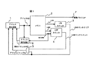
図1は本発明によるタイミングパルス発生装置の一実施形態を示すブロック図であって、1はアドレス発生回路、2はメモリ、3はLEN(長さ)カウンタ、4はLOOP(ループ)カウンタ、5はアンドゲート、6はアドレス保持回路、7は出力端子である。 FIG. 1 is a block diagram showing an embodiment of a timing pulse generator according to the present invention, wherein 1 is an address generating circuit, 2 is a memory, 3 is a LEN (length) counter, 4 is a LOOP (loop) counter, 5 Is an AND gate, 6 is an address holding circuit, and 7 is an output terminal.
同図において、メモリ2の記憶エリアは、駆動パルスDPや、設定データとしてのLEN(長さ)データ及びLOOP(繰り返し周期)データ、制御データとしてのRETURN(戻り)データなどのデータ毎にデータ格納エリアが区分されており、夫々のデータ格納エリアでは、各アドレス毎に順次データの値が格納されている。かかるアドレスはアドレス発生回路1から発生されるアドレス信号によって指定され、各データ格納エリアでは、このアドレス信号によって指定されるアドレスからそこに格納されているデータ値が読み出される。
In the figure, the storage area of the
アドレス発生回路1は、所定のタイミングで供給されるリセットパルスRによってアドレスADが値「0」にリセットされ、また、後述するLENカウンタ3から出力されるレベル“H”(高レベル)のLENカウンタクリア信号の立下りエッジにより、あるいは、アンドゲート5から出力されるレベル“H”のアドレスジャンプパルスAJの立下りエッジにより、アドレスADを更新する。
The
メモリ2から出力されるLENデータはLENカウンタ3にセットされる。LENカウンタ3はクロックφを初期値「1」からカウントアップし、このカウント値がセットされたLENデータの値と等しくなると、クロックφの1周期の時間幅でレベル“H”のLENカウンタクリアパルスを発生し、また、カウント値を初期値「1」に戻す。
The LEN data output from the
アドレス発生回路1は、このLENカウンタクリアパルスのレベル“H”からレベル“L”(低レベル)への立下りエッジのタイミングでインクリメントし、次の値「1」だけ増加したアドレスADをメモリ2に供給する。そこで、メモリ2では、各データ格納エリアのこのアドレスADで指定されるアドレスから次のデータ値が読み出される。読み出されたLENデータはLENカウンタ3にセットされ、LENカウンタ3は、上記のように、初期値「1」からクロックφをカウントアップする。
The
また、アドレス発生回路1からのアドレスADに応じてメモリ2から出力されるLOOPデータが、LOOPカウンタ4にセットされる。このLOOPカウンタ4は、アドレス発生回路1からのアドレスADに応じてメモリ3から出力される“1”(高レベル),“0”(低レベル)のRETURNデータのレベル“1”からレベル“0”への立下りエッジ毎にインクリメントし、RETURNデータのレベル“1”で、かつLOOPカウンタ4のカウント値がそのときセットされているLOOPデータと一致しないとき、LOOPインクリメントパルスを発生する。
Further, LOOP data output from the
ここで、RETURNデータが“0”のとき、アドレス保持回路6にこのときのアドレスADが、保持アドレスHADとして、アドレス保持回路6に保持される。
Here, when the RETURN data is “0”, the address AD at this time is held in the
LENカウンタ3から出力されるLENカウンタクリアパルスとLOOPカウンタ4から出力されるLOOPインクリメントパルスとはアンドゲート5で演算処理され、これらLENカウンタクリアパルスとLOOPインクリメントパルスとがともにレベル“H”のとき、制御信号としてのアドレスジャンプパルスAJが生成される。アドレス発生回路1は、通常、LENカウンタ3からのLENカウンタクリアパルスの立下りエッジ毎に順次インクリメントするアドレスADを生成出力するが、アンドゲート5からアドレスジャンプパルスAJが供給されると、これによる制御により、アドレス保持回路6に保持されている保持アドレスHADにアドレスADをクリアする(戻す)。従って、このときのアドレスADはこの保持アドレスHADとなり、次にアンドゲート5からアドレスジャンプパルスAJが供給されるまで、LENカウンタ3からのLENカウンタクリアパルスの立下りエッジ毎にアドレスADをこの保持アドレスHADから順次インクリメントする。
The LEN counter clear pulse output from the
このようにして、アドレス発生回路1は、メモリ2から読み出されるLENデータ,LOOPデータ,RETURNデータに応じたアドレスADを発生し、かかるアドレスADによってメモリ2から駆動パルスDPが読み出され、出力端子7から外部に出力される。
In this way, the
次に、この実施形態の動作の一具体例について説明する。 Next, a specific example of the operation of this embodiment will be described.
ここで、メモリ2には、図2に示すように、データが格納されているものとする。なお、図2は各データ格納エリアでのアドレスAD毎のデータを模式的に示すものであって、例えば、LENデータ格納エリア2aには、アドレスADが「0」,「1」,「2」,「3」,「4」の順に値「2」,「3」,「4」,「2」,「2」のLENデータが格納されており、LOOPデータ格納エリア2bには、アドレスADが「0」,「1」,「2」,「3」,「4」の順に値「2」,「2」,「1」,「1」,「1」のLOOPデータが格納されており、RETURNデータ格納エリア2cには、アドレスADが「0」,「1」,「2」,「3」,「4」の順にレベル“0”,“1”,“0”,“0”,“0”のRETURNデータが格納されており(但し、レベル“0”は低レベル、レベル“1”は高レベルとする)、駆動パルス格納エリア2dには、アドレスADが「0」,「1」,「2」,「3」,「4」の順にレベル“L”,“H”,“L”,“H”,“L”の駆動パルスDPのデータが格納されている。
Here, it is assumed that data is stored in the
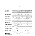
図3はクロックφの周期毎のタイミングを基準とした図1の各部のデータ,信号を示すタイミング図であって、クロックφの周期毎のタイミングをφ1,φ2,φ3,……,φ18で示す。 FIG. 3 is a timing diagram showing the data and signals of each part of FIG. 1 with reference to the timing of each cycle of the clock φ, and the timing of each cycle of the clock φ is represented by φ1, φ2, φ3,. .
以下では、図1〜図3により、各タイミング(クロックφ1,φ2,φ3,……,φ18)毎に動作を説明する。 Hereinafter, the operation will be described for each timing (clocks φ1, φ2, φ3,..., Φ18) with reference to FIGS.
A.クロックφ1〜φ10の期間について
(1)クロックφ1のタイミング:
このタイミングでは、アドレス発生回路1がリセットパルスRでリセットされ、アドレス発生回路1から出力されるアドレスADを「0」となる。これにより、クロックφ1のタイミングでは、メモリ2の各データ格納エリア2a〜2dから値「2」のLENデータ、値「2」のLOOPデータ、及び“0”のRETURNデータが読み出され、値「2」のLENデータはLENカウンタ3に、値「2」のLOOPデータはLOOPカウンタ4に夫々セットされる。このとき、LENカウンタ3とLOOPカウンタ4とのカウント値は初期値「1」にリセットされ、夫々のセット値と一致しない。従って、LENカウンタ3からは“H”のLENカウンタクリアパルスが出力されず、LOOPカウンタ4からも、“H”のLOOPインクリメントパルスは出力されない。
A. Regarding the period of clocks φ1 to φ10 (1) Timing of clock φ1:
At this timing, the
また、このクロックφ1のタイミングでは、RETURNデータが“0”であるから、アドレス保持回路6にこのときのアドレスAD、即ち、「0」のアドレスADが保持される。
Further, since the RETURN data is “0” at the timing of the clock φ1, the address AD at this time, that is, the address AD of “0” is held in the
さらに、図2により、この「0」のアドレスADでは、メモリ2での駆動パルスのデータ格納エリアに“L”のデータが格納されており、このため、この“L”のデータが読み出されて駆動パルスDPは“L”を出力する。
Further, as shown in FIG. 2, at the address AD of “0”, “L” data is stored in the data storage area of the drive pulse in the
(2)クロックφ2のタイミング:
次のクロックφ2のタイミングでは、LENカウンタ3がクロックφをアップカウントしてそのカウント値が「2」となり、LENカウンタ3のセット値「2」と等しくなる。これにより、このLENカウンタ3から“H”のLENカウンタクリアパルスが出力される。しかし、このときも、アドレス発生回路1からのアドレスADがそのまま「0」に保持されているので、メモリ2からのRETURNデータは“0”であり、LOOPカウンタ4はアップカウントしないで、そのカウント値がそのまま初期値「1」に保持される。従って、LOOPカウンタ4からは“H”のLOOPインクリメントパルスは出力されない。
(2) Timing of clock φ2:
At the
さらに、図2により、このときのアドレスADは「0」であり、メモリ2の駆動パルスDPのデータ格納エリアのアドレス「0」に“L”のデータが格納されているので、メモリ2からは“L”の駆動パルスDPが出力される。
Further, according to FIG. 2, the address AD at this time is “0”, and “L” data is stored in the address “0” of the data storage area of the drive pulse DP of the
(3)クロックφ3のタイミング:
次のクロックφ3のタイミングでは、LENカウンタ3がクロックφをアップカウントする際に、クロックφ2のタイミング時において、LENカウンタ3から“H”のLENカウンタクリアパルスが出力されていることから、事前に「次のクロックφのタイミング、即ち、クロックφ2からクロックφ3への切換えタイミングでは、LENカウンタ3はカウント値を初期値「1」にリセットする」ことが判っているため、立下りエッジで初期値「1」にリセットされ、同時に、LENカウンタクリアパルスは立ち下がる。
(3) Timing of clock φ3:
At the next clock φ3 timing, when the
一方、クロックφ3のタイミングでLENカウンタ3からのLENカウンタクリアパルスが立ち下がることにより、その立下りエッジでアドレス発生回路1がインクリメントし、アドレスADが「1」となる。
On the other hand, when the LEN counter clear pulse from the
これにより、メモリ2での各データ格納エリアでアドレス「1」がアクセスされ、図2により、メモリ2から値「3」のLENデータが読み出されてLENカウンタ3にセットされる。また、メモリ2から値「2」のLOOPデータが読み出されてLOOPカウンタ4にセットされるが、このセット値はクロックφ1のタイミングのときのセット値と変わりがない。
As a result, the address “1” is accessed in each data storage area in the
このようにして、クロックφ3のタイミングでは、アドレスADが「1」であって、LENカウンタ3は値「3」にセットされ、LOOPカウンタ4は値「2」にセットされている。
Thus, at the timing of the clock φ3, the address AD is “1”, the
一方、図2により、アドレスADが「1」となると、メモリ2から出力されるRETURNデータは“1”となるが、LOOPカウンタ4はこの立上りエッジではアップカウントせず、そのカウント値はそのまま「1」に保持される。但し、このカウント値「1」はこのLOOPカウンタ4のセット値「2」と異なっており、しかも、RETURNデータが“1”となったことから、LOOPカウンタ4から“H”のLOOPインクリメントパルスが出力される。
On the other hand, according to FIG. 2, when the address AD becomes “1”, the RETURN data output from the
なお、図2により、メモリ2の駆動パルスDPのデータ格納エリアのアドレス「1」に“H”のデータが格納されているので、メモリ2から“H”の駆動パルスDPが読み出されて出力端子7から出力される。
2, since “H” data is stored in the address “1” of the data storage area of the drive pulse DP of the
また、RETURNデータが“1”であるので、アドレス保持回路6の書き替えが行なわれず、その保持アドレスHADは「0」のままである。
Further, since the RETURN data is “1”, the
(4)クロックφ4のタイミング:
次のクロックφ4のタイミングでは、LENカウンタ3がクロックφをアップカウントしてそのカウント値が「2」となるが、これがLENカウンタ3のセット値「3」と一致しないので、“H”のLENカウンタクリアパルスは発生しない。このため、アドレス発生回路1からのアドレスADは「1」のままである。そこで、メモリ2からのRETURNデータは“1”のままであり、LOOPカウンタ4のカウント値は初期値「1」のままであって、“H”のLOOPインクリメントパルスの出力がそのまま継続する。
(4) Timing of clock φ4:
At the timing of the next clock φ4, the
なお、このクロックφ4のタイミングでも、“H”の駆動パルスDPがメモリ2から読み出され続ける。
Note that the drive pulse DP of “H” is continuously read from the
(5)クロックφ5のタイミング:
次のクロックφ5のタイミングでは、LENカウンタ3がクロックφをアップカウントしてそのカウント値が「3」となり、LENカウンタ3のセット値「3」と等しくなる。これにより、LENカウンタ3から“H”のLENカウンタクリアパルスが出力され始める。このときも、LOOPカウンタ4のカウント値は初期値「1」のままであって、そのセット値「2」とは一致せず、また、RETURNデータは“1”のままであるから、“H”のLOOPインクリメントパルスが出力され続ける。
(5) Timing of clock φ5:
At the timing of the next clock φ5, the
このように、クロックφ5のタイミングでは、LENカウンタクリアパルスとLOOPインクリメントパルスとがともに“H”であるから、アンドゲート5から“H”のアドレスジャンプパルスAJが出力される。
Thus, at the timing of the clock φ5, since both the LEN counter clear pulse and the LOOP increment pulse are “H”, the AND
(6)クロックφ6のタイミング〜クロックφ10のタイミング:
次のクロックφ6のタイミングでは、クロックφ2からクロックφ3への切り換わりと同様、事前に次のクロックφでLENカウンタ3が初期値にリセットされることが判るため、その立下りエッジでLENカウンタ3が初期値「1」にリセットされ、同時に、LENカウンタクリアパルスが立ち下がる。また、アンドゲート5の出力レベルが“L”になってアドレスジャンプパルスAJが立ち下がる。このアドレスジャンプパルスAJの立下りエッジでアドレス保持回路6の「0」の保持アドレスHADがアドレス発生回路1に取り込まれ、アドレスADがこの保持アドレスHADに等しい値「0」に設定される。従って、メモリ2からは、上記クロックφ1のタイミングのときと同じ値「2」のLENデータが読み出されてLENカウンタ3にセットされ、また、上記クロックφ1のタイミングのときと同じ値「2」のLOOPデータが読み出されてLOOPカウンタ4にセットされる。
(6) Timing of clock φ6 to timing of clock φ10:
At the timing of the next clock φ6, it is known that the
また、アドレスADが「0」となったことにより、図2により、メモリ2からのRETURNデータが“1”から“0”に反転する。これにより、LOOPカウンタ4からのLENカウンタクリアパルスは“1”から“0”にレベル反転して立ち下がる。従って、アンドゲート5の出力は“L”になる。
Since the address AD becomes “0”, the RETURN data from the
さらに、RETURNデータが“1”から“0”にレベル反転することにより、この時点でのアドレスAD、即ち、値「0」のアドレスADがアドレス保持回路6に、保持アドレスHADとして、保持される。
Further, the level of the RETURN data is inverted from “1” to “0”, so that the address AD at this time, that is, the address AD having the value “0” is held in the
このようにして、LENカウンタ3とLOOPカウンタ4とに夫々値「2」がセットされることにより、クロックφ1のタイミングからクロックφ5までの上記の動作が繰り返されることになる。この期間がクロックφ6のタイミングからクロックφ10のタイミングまでの期間である。この期間でも、アドレス値ADが「1」の期間、メモリ2から“H”の駆動パルスDPが読み出されて出力端子7から出力される。
In this way, when the value “2” is set in the
但し、かかる期間でのLOOPカウンタ4のカウント値は「2」であり、LOOPカウンタ4のセット値と等しい値となっている。従って、アドレスADが「1」となってRETURNデータが“1”となっても、LOOPカウンタ4からは“H”のLOOPインクリメントパルスは発生せず、従って、アンドゲート5からはアドレスジャンプパルスAJが発生しない。
However, the count value of the
以上のようにして、クロックφ1〜φ10の期間、クロックφの5倍の周期5Tφでデューティ比60%(=3×100/5)の駆動パルスDPがメモリ2から2回出力されることになる。
As described above, the drive pulse DP having a duty ratio of 60% (= 3 × 100/5) is output from the
B.クロックφ11〜φ18の期間について
(7)クロックφ11のタイミング:
クロックφ10のタイミングでは、先のクロックφ5のタイミングのときと同様、LENカウンタ3のカウント値は「3」でそのセット値と等しく、このLENカウンタ3からは“H”のLENカウンタクリアパルスが出力されているため、次のクロックφ11のタイミングでクロックφにより、LENカウンタ3を初期値にリセットすることが事前に判るため、クロックφで初期値にリセットされる。同時に、LENカウンタクリアパルスは“H”から“L”に反転して立ち下がる。このLENカウンタクリアパルスの立下りエッジでアドレス発生回路1はインクリメントし、そのアドレスADを「2」とする。
B. Regarding the period of clocks φ11 to φ18 (7) Timing of clock φ11:
At the timing of the clock φ10, similarly to the timing of the previous clock φ5, the count value of the
そこで、メモリ2では、各データ格納エリアのアドレス「2」が読み出されることになり、図2により、値「4」のLENデータが読み出されてLENカウンタ3にセットされ、値「1」のLOOPデータが読み出されてLOOPカウンタ4にセットされる。また、“0”のRETURNデータが読み出されてLOOPカウンタ4とアドレス保持回路6とに供給される。このRETURNデータが“0”となったことにより、また、このときのLOOPカウンタ4のカウント値「2」がそのセット値と一致していることから、LOOPカウンタ4のカウント値は初期値「1」にリセットされ、また、RETURNデータが“0”であることから、アドレス保持回路6にそのときの「2」のアドレスADが、保持アドレスHADとして、保持される。
Therefore, in the
(8)クロックφ12のタイミング〜クロックφ13のタイミング:
次のクロックφ12のタイミングでLENカウンタ3がクロックφをアップカウントしてそのカウント値が「2」となり、さらに、次のクロックφ13のタイミングでLENカウンタ3がクロックφをアップカウントしてそのカウント値が「3」となるが、これらカウント値はセット値「4」に一致しないので、LENカウンタ3から“H”のLENカウンタクリアパルスが発生しない。
(8) Timing of clock φ12 to timing of clock φ13:
The
また、このときのLOOPカウンタ4のカウント値「1」はそのセット値「1」と一致しているので(仮に、RETURNデータが“1”となっても)、LOOPカウンタ4も“H”のLOOPインクリメントパルスを発生しない。
At this time, the count value “1” of the
従って、LENカウンタ3がクロックφをアップカウントするだけで、これ以外は同じ状態が維持される。
Therefore, the
(9)クロックφ14〜φ15のタイミング:
次のクロックφ14のタイミングでLENカウンタ3がクロックφをアップカウントしてそのカウント値が「4」となると、これがLENカウンタ3のセット値に等しくなるから、LENカウンタ3から“H”のLENカウンタクリアパルスが発生する。しかし、LOOPカウンタ4は、そのカウント値「1」がそのセット値と一致しているので“H”のLOOPインクリメントパルスを発生しない。
(9) Timing of clocks φ14 to φ15:
When the
そして、次のクロックφ15のタイミングになると、クロックφ2,φ3,φ5,φ6,φ7,φ8,φ10,φ11などと同様に、LENカウンタ3が初期値にリセットされ、同時に、“H”のLENカウンタクリアパルスは“H”から“L”へ立ち下がり、この立下りエッジでアドレス発生回路1がインクリメントし、アドレスADが「3」となる。
Then, at the timing of the next clock φ15, the
アドレスADが「3」になると、図2により、メモリ2から値「2」のLENデータが読み取られてLENカウンタ3にセットされ、値「1」のLOOPデータが読み取られてLOOPカウンタ4にセットされる。また、“0”のRETURNデータが読み取られてLOOPカウンタ4とアドレス保持回路6に供給される。これにより、アドレス保持回路6には、そのときの「3」のアドレスADが保持される。しかし、LOOPカウンタ4からは“H”のLOOPインクリメントパルスは発生しない。
When the address AD becomes “3”, the LEN data with the value “2” is read from the
また、アドレスADが「3」のときには、メモリ2から“H”の駆動パルスDPが読み取られ、出力端子7から出力される。
When the address AD is “3”, the “H” drive pulse DP is read from the
(10)クロックφ16のタイミング:
次のクロックφ16のタイミングでLENカウンタ3がクロックφをアップカウントしてそのカウント値が「2」となると、これがLENカウンタ3のセット値と等しいから、LENカウンタ3から“H”のLENカウンタクリアパルスが出力される。しかし、LOOPカウンタ4は、そのカウント値「1」がそのセット値に等しいから、“H”のLOOPインクリメントパルスを発生しない。このときも、RETURNデータが“0”であるから、「3」のアドレスADがアドレス保持回路6に保持される。また、このときのアドレスADが「3」であるから、メモリ2から駆動パルスDPは発生している。
(10) Timing of clock φ16:
When the
(11)クロックφ17のタイミング:
次のクロックφ17のタイミングでLENカウンタ3が初期値にリセットされ、同時に、LENカウンタクリアパルスが“H”から“L”へ立ち下がる。このLENカウンタクリアパルスの立下りエッジにより、アドレス発生回路1はインクリメントし、アドレスADは「4」となる。
(11) Timing of clock φ17:
At the timing of the next clock φ17, the
アドレスADが「4」になると、図2により、メモリ2から値「2」のLENデータが読み取られてLENカウンタ3にセットされ、値「1」のLOOPデータが読み取られてLOOPカウンタ4にセットされる。また、“0”のRETURNデータが読み取られてLOOPカウンタ4とアドレス保持回路6に供給される。これにより、アドレス保持回路6には、そのときの「4」のアドレスADが保持される。しかし、LOOPカウンタ4からは“H”のLOOPインクリメントパルスは発生しない。
When the address AD becomes “4”, the LEN data having the value “2” is read from the
また、アドレスADが「4」となると、メモリ2から出力されていた駆動パルスDPが立ち下がり、“L”を出力する。
When the address AD is “4”, the drive pulse DP output from the
(12)クロックφ18のタイミング:
次のクロックφ18のタイミングでLENカウンタ3がクロックφをアップカウントしてそのカウント値が「2」となると、これがLENカウンタ3のセット値と等しいから、LENカウンタ3から“H”のLENカウンタクリアパルスが出力される。しかし、LOOPカウンタ4は、そのカウント値「1」がそのセット値に等しいから、“H”のLOOPインクリメントパルスを発生しない。このときも、RETURNデータが“0”であるから、「4」のアドレスADがアドレス保持回路6に、保持アドレスHADとして、保持される。また、このときのアドレスADが「4」であることにより、メモリ2から駆動パルスDPは発生しない。
(12) Timing of clock φ18:
When the
以上の動作説明から明らかなように、LENデータは、アドレスADの期間長を、クロックφの周期Tφを単位長として、規定するものである。例えば、LENデータの値が「2」であるときには、例えば、「0」のアドレスADの期間長が2Tφとなる。このことから、LENデータに応じて駆動パルスDPの周期やパルス幅が規定されることになる。 As apparent from the above description of operation, LEN data, the period length of the address AD, a unit length period T phi clock phi, it prescribes. For example, when the value of the LEN data is “2”, for example, the period length of the address AD of “0” is 2T φ . From this, the cycle and pulse width of the drive pulse DP are defined according to the LEN data.
また、上記の例では、アドレスADが「1」であるクロックφ3〜φ5のタイミング期間及びクロックφ8〜φ10のタイミング期間や、アドレスADが「3」であるクロックφ15〜φ16のタイミング期間に駆動パルスDPがメモリ2から出力される。
In the above example, the driving pulse is generated in the timing period of the clocks φ3 to φ5 and the timing period of the clocks φ8 to φ10 where the address AD is “1”, and the timing period of the clocks φ15 to φ16 where the address AD is “3”. DP is output from the
ここで、クロックφ1〜φ10のタイミングの期間では、クロックφの周期の5倍の周期5Tφで2回駆動パルスDPが発生されるものである。これは、「0」,「1」のアドレスADが続く期間を2回繰り返すことによって可能としており、この繰り返しはLOOPデータによって決められるものである。上記のタイミング期間の例では、アドレス値ADが「0」,「1」であるときのLOOPデータの値を「2」としているため、アドレス値ADが「0」,「1」の期間を2回繰り返すことになるが、LOOPデータを値「2」以上の値とすることにより、「0」,「1」のアドレス値ADが続く期間を任意回数繰り返すようにすることができ、一定周期の駆動パルスを任意個数を発生させることができる。 Here, in the timing period of the clocks φ1 to φ10, the drive pulse DP is generated twice with a period 5T φ that is five times the cycle of the clock φ. This is made possible by repeating the period in which the addresses AD of “0” and “1” continue twice, and this repetition is determined by the LOOP data. In the example of the above timing period, the value of the LOOP data when the address value AD is “0” and “1” is “2”, so the period when the address value AD is “0” and “1” is 2 However, by setting the LOOP data to a value equal to or greater than “2”, the period in which the address value AD of “0” and “1” continues can be repeated any number of times. An arbitrary number of drive pulses can be generated.
但し、このように、「0」,「1」のアドレスADを繰り返させる場合、「0」のアドレスADをアドレス保持回路6に、保持アドレスHADとして、保持し、「1」のアドレスADの経過後、アドレス保持回路6に保持されているこの「0」の保持アドレスHADをアドレス発生回路1に供給して、アドレスADを「0」に戻す。このアドレスADは、保持アドレスHADとして、アドレス保持回路6に保持される。かかる動作をLOOPデータの値の回数繰り返すのであるが、アドレス保持回路6へのアドレスADの保持タイミングとアドレス発生回路1への保持アドレスHADの供給タイミングをRETURNデータの“0”,“1”で規定しているのである。
However, when the address AD of “0” and “1” is repeated in this way, the address AD of “0” is held in the
例えば、アドレスADが「0」,「1」のときにメモリ2から読み出されるLOOPデータの値が「3」の場合には、図4に示すように、LOOPカウンタ4は、初期値「1」から、RETURNデータが“1”から“0”にレベル反転する立下りエッジ毎に、インクリメントし、そのカウント値が「1」,「2」,「3」でアドレスADが「1」となる毎に駆動パルスDPを発生し、駆動パルスDPを3回発生することになる。
For example, when the value of the LOOP data read from the
なお、LOOPデータの値が「1」である場合には、図3でのクロックφ11〜φ18のタイミングの期間のように、アドレス発生回路1から順次インクリメントされるアドレスADが発生される状態となり、メモリ2での駆動パルスDPのデータ格納エリアでの適宜のアドレスで“H”のデータを格納しておくことにより、適宜のタイミングで駆動パルスDPをメモリ2から出力させるようにすることができる。
When the value of the LOOP data is “1”, the address AD sequentially incremented from the
以上のようにして、この第1の実施形態では、メモリ2の格納されているLENデータ,LOOPデータ,RETURNデータがアドレス発生回路1からのアドレスADに応じて読み出され、これら読み出されたこれらデータに応じてアドレス発生回路1からのアドレスADが制御されることにより、メモリ2からそこに格納されているデータに応じた所望のパターンの駆動パルスDPを得ることができる。
As described above, in the first embodiment, the LEN data, the LOOP data, and the RETURN data stored in the
そして、一定周期の駆動パルスDPを連続して発生させる場合には、メモリ2の同じアドレスを繰り返し読み出すことが可能であるから、同じパルスパターン、周期やパルス幅が一定の駆動パルスを繰り返し読み出すことが可能となって、かかる駆動パルスを、僅かなメモリ容量を利用して、発生させることができ、メモリの使用効率が大幅に向上する。
When driving pulses DP having a constant cycle are generated continuously, the same address in the
また、この第1の実施形態によると、異なるパルスパターンの複数種のパルス列からなる駆動パルスを発生させるにしても、夫々のパルスパターンのパルス列のデータをメモリ2の格納するだけで発生させることができ、しかも、夫々、パルスパターンのパルス列を発生させるためのデータを格納するに要するメモリ容量は、上記のように、少なくて済むし、また、かかるデータを容易に追加格納することが可能であるから、回路構成を変更することなく、異なるパルスパターンの駆動パルスや、種々のパルスパターンのパルス列からなる変化点の数が異なる駆動パルスを使用する機器にも、適用可能である。即ち、任意のパルスパターンの駆動パルスを用いる機器に対して、この第1の実施形態は、回路構成を変更することなく、適用可能である。
Further, according to the first embodiment, even when driving pulses composed of a plurality of types of pulse trains having different pulse patterns are generated, the data of the pulse trains of the respective pulse patterns can be generated only by storing them in the
ところで、この第1の実施形態では、図2から明らかなように、アドレスADが「1」,「3」のとき、“H”の駆動パルスDPがメモリ2から出力されることになる。このことは、デジタル値であるアドレス値ADの最下位ビットが“1”のとき、“H”の駆動パルスDPが発生することを意味している。
In the first embodiment, as is apparent from FIG. 2, when the address AD is “1” or “3”, the drive pulse DP of “H” is output from the
図5はこのことを利用して駆動パルスDPを得ることができるようにした本発明によるタイミングパルス発生装置の第2の実施形態を示すブロック図であって、2’はメモリ、8は信号線であり、図1に対応する部分には同一符号を付けて重複する説明を省略する。 FIG. 5 is a block diagram showing a second embodiment of the timing pulse generator according to the present invention, which makes it possible to obtain a drive pulse DP by utilizing this fact, 2 ′ is a memory, and 8 is a signal line. Therefore, portions corresponding to those in FIG.
また、図6は図5における各部のデータ,信号を示すタイミング図である。 FIG. 6 is a timing chart showing data and signals of respective parts in FIG.
図5において、メモリ2’には、LENデータ,LOOPデータ及びRETURNデータ夫々のデータ格納エリアが設けられ、図1におけるメモリ2と同様、その各アドレス毎に図2に示すLENデータ,LOOPデータ,RETURNデータが格納されている。しかし、このメモリ2’には、駆動パルスDPのデータ格納エリアは設けられていない。
In FIG. 5, the
この第2の実施形態においても、アドレス発生回路1からのアドレスADに応じたLENデータ,LOOPデータ,RETURNデータが読み出され、かかるデータに応じて、図6に示すように、LENカウンタ3,LOOPカウンタ4,アンドゲート5,アドレス保持回路6及びアドレス発生回路1が図1におけるこれら回路と同様の動作を行なう。
Also in the second embodiment, the LEN data, the LOOP data, and the RETURN data corresponding to the address AD from the
ここで、この第2の実施形態では、アドレス発生回路1からのアドレスADが奇数値のとき、“H”の駆動パルスDPが出力されるように構成されている。即ち、アドレス発生回路1から出力されるアドレスADは複数ビットからなるパラレルデジタルデータであり、アドレスADの信号線の最下位ビット(LSB)から引き出される信号線8が“H”の駆動パルスDPの出力線となっている。アドレスADが奇数値であるときには、アドレスADのLSBは“1”で“H”レベルであり、従って、図6に示すように、アドレスADが値「1」,「3」のとき、“H”の駆動パルスDPが信号線8を通して出力される。
Here, in the second embodiment, when the address AD from the
この第2の実施形態では、先の第1の実施形態と同様の効果が得られるが、さらに、実質的には、アドレス発生回路1が駆動パルスDPの発生回路ともなっており、メモリ2’は駆動パルスDPのデータを格納しておく必要がなく、メモリの利用効率がさらに向上して、メモリ2’の使用効率が、図1でのメモリ2に比べて、さらに向上することになる。
In the second embodiment, the same effects as those of the first embodiment can be obtained. However, substantially, the
次に、本発明によるタイミングパルス発生装置を使用する機器の例として、CCD撮像装置について説明する。 Next, a CCD imaging device will be described as an example of a device using the timing pulse generator according to the present invention.
図7は本発明によるタイミングパルス発生装置を使用した本発明による撮像装置の一実施形態の要部を示すブロック図であって、10はCCD撮像素子、11は信号処理回路、12はV(垂直)ドライバ、13はタイミングパルス発生装置である。
FIG. 7 is a block diagram showing the main part of an embodiment of the imaging apparatus according to the present invention using the timing pulse generator according to the present invention, wherein 10 is a CCD imaging device, 11 is a signal processing circuit, and 12 is V (vertical). ) A
同図において、タイミングパルス発生装置13からは、水平転送用パルスφHと垂直転送用パルスφVとが発生される。水平転送用パルスφHはCCD撮像素子10に供給され、垂直転送用パルスφVは、Vドライバ12で、例えば、−9V〜21Vの電圧に増幅された後、CCD撮像素子10に供給される。CCD撮像素子10では、周知のように、垂直転送用CCD(図示せず)に取り込まれた画素電荷が垂直転送用パルスφVによって垂直転送され、水平転送用CCD(図示せず)に送られる。この水平転送用CCDでは、垂直転送用CCDから送られてきた画素電荷が水平転送用パルスφHによって水平転送され、映像信号として、CCD撮像素子10から出力される。この映像信号は、信号処理回路11で処理される。
In the figure, the
タイミングパルス発生装置13は、垂直転送用パルスφVの発生用としてのタイミングパルス発生装置と水平転送用パルスφHの発生用としてのタイミングパルス発生装置とからなり、これらタイミングパルス発生装置として、上記各実施形態として示す本願発明によるタイミングパルス発生装置が使用される。
The
図8は図7におけるCCD撮像素子10の撮像画面での各動作期間の一具体例を示す図である。
FIG. 8 is a diagram showing a specific example of each operation period on the imaging screen of the
同図において、この具体例では、撮像画面14の一部を実際に撮像画面を得るための有効領域15とする。この有効領域15がアスペクト4:3の画面領域である。この有効領域15での電荷が有効な電荷として取り込まれ、かかる有効な電荷からなる信号が、CCD撮像素子10の出力映像信号として、信号処理回路11に供給される。そして、撮像画面14でのこの有効領域15を除いた領域での電荷は、破棄される。
In this figure, in this specific example, a part of the
CCD撮像素子10の垂直転送用CCDでの垂直転送についてみると、有効領域15での電荷を読み取る垂直有効期間T0,1では、通常速度による通常転送が行なわれ、この有効領域15以外の領域での電荷を掃き出す電荷掃出期間T7,8、T3,4では、高速転送が行なわれる。電荷掃出期間T7,8は、センサ(光電変換素子)からの電荷の読出しに続いて電荷を掃き出しを行なう期間であり、また、電荷掃出期間T3,4は、垂直有効期間T0,1後に電荷を掃き出しを行なう期間である。
Regarding vertical transfer in the CCD for vertical transfer of the CCD
なお、1フィールドについてみると、垂直有効期間T0,1は250ライン(水平走査線)分の期間であり、電荷掃出期間T7,8と電荷掃出期間T3,4との合計は一定のライン数分の期間(例えば、100ライン)である。このように、映像信号を得るための有効領域15を撮像画面14の一部としたのは、この有効領域15を撮像画面14内で上下、左右に移動できるようにするためであり、これにより、手ぶれなどによる再生画面の揺れを防止できるようにしている。
As for one field, the vertical effective period T 0,1 is a period corresponding to 250 lines (horizontal scanning lines), and the sum of the charge sweep period T 7,8 and the charge sweep period T 3,4 is A period corresponding to a certain number of lines (for example, 100 lines). Thus, the reason why the
図9は図8に示す撮像画面14についての垂直転送のための1フィールド期間での垂直転送用パルスφVの一具体例を示す図であって、VD(垂直同期信号)/HD(水平同期信号)のタイミングと対応させて示している。
FIG. 9 is a diagram showing a specific example of the vertical transfer pulse φ V in one field period for vertical transfer for the
同図において、期間T0,1は、図8における有効領域15での画素を垂直転送する垂直有効期間T0,1であり、このときの垂直転送用パルスφVは画素を水平転送用CCDに転送するための通常転送を行なうものである。この垂直有効期間T0,1に続いて、“L”の期間T2が設けられ、これに続いて期間T3,4が設けられている。この期間T3,4は、図8における撮像画面14での有効領域15よりも下部の領域に対する電荷掃き出しのための垂直転送期間、即ち、電荷掃出期間T3,4であり、この電荷掃出期間T3,4の垂直転送用パルスφVは画素を高速転送するものである。
In the figure, a period T 0,1 is a vertical effective period T 0,1 in which the pixels in the
この電荷掃出期間T3,4に続く期間T5,6は、各センサから垂直転送用CCDに電荷を転送する期間である。次の期間T7,8は、図8における撮像画面14での有効領域15よりも上部の領域に対する電荷掃き出しのための垂直転送期間、即ち、電荷掃出期間T7,8であり、この電荷掃出期間T7,8の垂直転送用パルスφVは画素を高速転送するものである。この電荷掃出期間T7,8が終了すると、“L”の期間T9を経て次の上記垂直有効期間T0,1に入る。
Periods T 5 and 6 subsequent to the charge sweep periods T 3 and 4 are periods in which charges are transferred from each sensor to the vertical transfer CCD. The next period T 7,8 is a vertical transfer period for sweeping out charges with respect to the area above the
以上が1フィールド(NTSC方式の場合、262.5H)期間での垂直転送用パルスφVの割り当てであるが、垂直転送用パルスφVの発生装置として図1または図5に示すタイミングパルス発生装置を用いる場合、メモリ2,2’に後述するデータを格納することにより、期間T0,1、T3,4、T5,6、T7,8毎にパルスパターン(即ち、周期やパルス幅など)が異なる一連のパルス列からなる垂直転送用パルスφVが得られる。
(The NTSC system, 262.5 H) or one field is a assignment of the vertical transfer pulse phi V in the period, the timing pulse generator shown in FIG. 1 or FIG. 5 as a generator of a vertical transfer pulse phi V Is stored in the
図10は図9に示す垂直転送用パルスφVを発生するための図1に示す第1の実施形態におけるメモリ2の各データ格納エリアでのデータを模式的に示す図である。
10 is a diagram schematically showing data in each data storage area of the
同図において、垂直有効期間T0,1では、メモリ2の読出アドレスを「0」,「1」とし、読出アドレスが「1」のときにRETURNデータを“1”とし、LOOPデータを値「250」として、アドレス「0」,「1」でのデータ読出しを5クロック周期(値「2」と「3」のLENデータ)5Tφで250回繰り返すものとしている。アドレス「2」のとき、“H”の駆動パルスが読み出され、この垂直有効期間T0,1では、250回駆動パルス(垂直転送用パルスφV)が発生することになる。
In the figure, in the vertical effective period T 0,1 , the read address of the
期間T2では、メモリ2の読出アドレスを「2」とし、RETURNデータ,LOOPデータを夫々値「1」として、アドレス「2」での“L”のデータ(駆動パルス)を1回読み出す。この期間長は、LENデータ=「4」であることから、4クロック周期の4Tφである。
In the period T 2 , the read address of the
また、電荷掃出期間T3,4と電荷掃出期間T7,8との合計水平ライン数を100としており、そのうちのn水平ラインは電荷掃出期間T7,8で電荷の掃出しが行なわれ、残りの(100−n)水平ラインは電荷掃出期間T3,4で電荷の掃出しが行なわれるものとしている。 In addition, the total number of horizontal lines of the charge sweep periods T3, 4 and the charge sweep periods T7, 8 is set to 100. Of these, n horizontal lines are subjected to charge sweeping during the charge sweep period T7, 8. is, the remaining (100-n) horizontal lines are assumed to sweeping charges is performed in the charge sweeping period T 3, 4.
そこで、電荷掃出期間T3,4では、メモリ2の読出アドレスを「3」,「4」とし、読出アドレスが「4」のときにRETURNデータを“1”とし、LOOPデータを値「100−n」として、アドレス「3」,「4」でのデータ読出しを4クロック周期(値「2」と「2」のLENデータ)4Tφで(100−n)回繰り返すものとしている。アドレス「3」のとき、“H”の駆動パルスが発生されるから、この電荷掃出期間T3,4では、(100−n)回高速に駆動パルス(垂直転送用パルスφV)が発生することになる。また、電荷掃出期間T7,8では、メモリ2の読出アドレスを「7」,「8」とし、読出アドレスが「8」のときにRETURNデータを“1”とし、LOOPデータを値「n」として、アドレス「7」,「8」でのデータ読出しを4クロック周期(値「2」と「2」のLENデータ)4Tφでn回繰り返すものとしている。アドレス「7」のとき、“H”の駆動パルスが発生されるから、この電荷掃出期間T7,8では、n回高速に駆動パルス(垂直転送用パルスφV)が発生することになる。
Therefore, in the charge sweep period T 3 , 4 , the read address of the
期間T5,6では、メモリ2の読出アドレスを「5」,「6」とし、読出アドレスが「6」のときにRETURNデータを“1”とし、LOOPデータを値「1」として、アドレス「5」,「6」でのデータ読出しを1回行なう。この場合、アドレス「5」のとき、“H”の駆動パルスDPが発生し、これがセンサから垂直転送用CCDに電荷を送るのに用いられる。
In the period T 5,6 , the read address of the
期間T9では、メモリ2の読出アドレスを「9」とし、RETURNデータを値「3」、LOOPデータを値「1」として、アドレス「9」での“L”のデータ(駆動パルス)を1回読み出す。この期間長は、LENデータ=「3」であることから、3クロック周期の3Tφである。
In the period T 9 , the read address of the
図11により、図10に示すデータをもとにしたときの図7におけるタイミングパルス発生装置13から発生される垂直転送用パルスφVの、一例として、垂直有効期間T0,1から電荷掃出期間T3,4へ移る部分を示す。
As an example of the vertical transfer pulse φ V generated from the
このようにして、タイミングパルス発生装置でのメモリに格納されたデータに応じて駆動パルスを得ることができるものであって、かかるメモリに所望とするデータを格納することにより、垂直転送用パルスφVなどのように、異なるパルスパターンのパルス列からなる一連の所望とする駆動パルスを発生させることができ、周期性を持つパルス列もわずかなメモリ容量を使用するだけで発生させることができるし、また、すでにデータが格納されているメモリにデータを追加することにより、新たなパルスパターンのパルス列を追加発生させることも可能である。 In this way, the drive pulse can be obtained according to the data stored in the memory in the timing pulse generator. By storing the desired data in the memory, the vertical transfer pulse φ A series of desired drive pulses consisting of pulse trains of different pulse patterns, such as V, can be generated, and pulse trains with periodicity can be generated using only a small memory capacity. It is also possible to generate an additional pulse train of a new pulse pattern by adding data to a memory that already stores data.
1 アドレス発生回路
2,2’ メモリ
3 LENカウンタ
4 LOOPカウンタ
5 アンドゲート
6 アドレス保持回路
7 出力端子
8 信号線
10 CCD撮像素子
11 信号処理回路
12 V(垂直)ドライバ
13 タイミングパルス発生装置
DESCRIPTION OF
Claims (3)
該アドレスに応じた設定データと制御データ,駆動パルスのデータが格納されたメモリと、
該メモリから読み出された第1の設定データとカウント結果を比較しながら、カウント動作を行ない、所定のタイミングでクリアパルスを発生する第1のカウンタと、
該メモリから読み出された第2の設定データとカウント結果を比較しながら、カウント動作を行ない、所定のタイミングでインクリメントパルスを発生する第2のカウンタと、
該アドレス発生回路で発生したアドレスを、該メモリから読み出される該制御データに応じたタイミングで、保持するアドレス保持回路と
を備え、
該アドレス発生回路は、該第1のカウンタからの該クリアパルス毎に該アドレスをインクリメントするとともに、該アドレスを、該第1のカウンタからの該クリアパルス及び第2のカウンタからの該インクリメントに応じて、該アドレス保持回路に保持された保持アドレスにジャンプさせ、該アドレスに応じて該メモリから駆動パルスを出力することを特徴とするタイミングパルス発生装置。 An address generation circuit for generating an address;
A memory storing setting data, control data, and driving pulse data corresponding to the address;
A first counter that performs a count operation while comparing the count result with the first setting data read from the memory, and generates a clear pulse at a predetermined timing;
A second counter that performs a count operation while comparing the count result with the second setting data read from the memory, and generates an increment pulse at a predetermined timing;
An address holding circuit for holding an address generated by the address generation circuit at a timing according to the control data read from the memory ;
The address generation circuit increments the address for each clear pulse from the first counter and determines the address in response to the clear pulse from the first counter and the increment from a second counter. A timing pulse generator that jumps to a holding address held in the address holding circuit and outputs a drive pulse from the memory in accordance with the address.
該アドレスに応じた設定データと制御データが格納されたメモリと、
該メモリから読み出された第1の設定データとカウント結果を比較しながら、カウント動作を行ない、所定のタイミングでクリアパルスを発生する第1のカウンタと、
該メモリから読み出された第2の設定データとカウント結果を比較しながら、カウント動作を行ない、所定のタイミングでインクリメントパルスを発生する第2のカウンタと、
該アドレス発生回路で発生したアドレスを、該メモリから読み出される該制御データに応じたタイミングで、保持するアドレス保持回路と
を備え、
該アドレス発生回路は、該第1のカウンタからの該クリアパルス毎に該アドレスをインクリメントするとともに、該アドレスを、該第1のカウンタからの該クリアパルス及び第2のカウンタからの該インクリメントに応じて、該アドレス保持回路に保持された保持アドレスにジャンプさせ、該アドレス発生回路から発生される該アドレスの所定ビットを駆動パルスとすることを特徴とするタイミングパルス発生装置。 An address generation circuit for generating an address;
A memory storing setting data and control data corresponding to the address;
A first counter that performs a count operation while comparing the count result with the first setting data read from the memory, and generates a clear pulse at a predetermined timing;
A second counter that performs a count operation while comparing the count result with the second setting data read from the memory, and generates an increment pulse at a predetermined timing;
An address holding circuit for holding an address generated by the address generation circuit at a timing according to the control data read from the memory ;
The address generation circuit increments the address for each clear pulse from the first counter and determines the address in response to the clear pulse from the first counter and the increment from a second counter. The timing pulse generator is characterized by jumping to a holding address held in the address holding circuit and using a predetermined bit of the address generated from the address generation circuit as a drive pulse.
Priority Applications (1)
| Application Number | Priority Date | Filing Date | Title |
|---|---|---|---|
| JP2005167142A JP4723919B2 (en) | 2005-06-07 | 2005-06-07 | Timing pulse generator and imaging device using the same. |
Applications Claiming Priority (1)
| Application Number | Priority Date | Filing Date | Title |
|---|---|---|---|
| JP2005167142A JP4723919B2 (en) | 2005-06-07 | 2005-06-07 | Timing pulse generator and imaging device using the same. |
Publications (3)
| Publication Number | Publication Date |
|---|---|
| JP2006345074A JP2006345074A (en) | 2006-12-21 |
| JP2006345074A5 JP2006345074A5 (en) | 2008-03-06 |
| JP4723919B2 true JP4723919B2 (en) | 2011-07-13 |
Family
ID=37641718
Family Applications (1)
| Application Number | Title | Priority Date | Filing Date |
|---|---|---|---|
| JP2005167142A Expired - Fee Related JP4723919B2 (en) | 2005-06-07 | 2005-06-07 | Timing pulse generator and imaging device using the same. |
Country Status (1)
| Country | Link |
|---|---|
| JP (1) | JP4723919B2 (en) |
Families Citing this family (2)
| Publication number | Priority date | Publication date | Assignee | Title |
|---|---|---|---|---|
| JP2009089085A (en) * | 2007-09-28 | 2009-04-23 | Sony Corp | Solid-state image pickup device, driving method thereof, and camera system |
| CN115988298B (en) * | 2023-03-16 | 2023-06-13 | 深圳市百盛兴业科技有限公司 | Camera for automobile reversing image |
Family Cites Families (2)
| Publication number | Priority date | Publication date | Assignee | Title |
|---|---|---|---|---|
| JP3204197B2 (en) * | 1998-01-26 | 2001-09-04 | ソニー株式会社 | CCD solid-state imaging device |
| JP2001339645A (en) * | 2000-05-25 | 2001-12-07 | Matsushita Electric Ind Co Ltd | Driver for solid-state image pickup element |
-
2005
- 2005-06-07 JP JP2005167142A patent/JP4723919B2/en not_active Expired - Fee Related
Also Published As
| Publication number | Publication date |
|---|---|
| JP2006345074A (en) | 2006-12-21 |
Similar Documents
| Publication | Publication Date | Title |
|---|---|---|
| JP6961392B2 (en) | Solid-state image sensor, image sensor and imaging method | |
| RU2458478C1 (en) | Solid-state image capturing device and driving method for said device | |
| JP4806595B2 (en) | Solid-state image sensor driving device and digital camera | |
| JP2001245218A (en) | Timing signal generator | |
| JP4723919B2 (en) | Timing pulse generator and imaging device using the same. | |
| JP2004040317A (en) | Timing signal generating apparatus, system, and imaging apparatus | |
| US6680751B1 (en) | Timing pulse generating apparatus | |
| JP3917428B2 (en) | Imaging device and imaging element driving pulse generation method | |
| JP4407621B2 (en) | Signal generator | |
| JP4424174B2 (en) | Imaging apparatus and imaging method | |
| JP6261210B2 (en) | Scanning circuit, photoelectric conversion device, and imaging system | |
| JP6541652B2 (en) | Image sensor with generation of control signal sequences | |
| US20040201762A1 (en) | Solid-state imaging apparatus | |
| JP2008141684A (en) | Timing pulse generating device, and ccd imaging device, cmos imaging device, lcd device and image sensor set using it | |
| JP2004248003A (en) | Imaging apparatus | |
| JP2943750B2 (en) | Timing pulse generation circuit | |
| JP3436281B2 (en) | Solid-state imaging device | |
| US20070040105A1 (en) | Driver for solid-state image sensing device | |
| KR101190429B1 (en) | Timing signal generating circuit and photographing device having the same | |
| JP3599514B2 (en) | Solid-state imaging device | |
| JP2008028608A (en) | Solid-state imaging device | |
| JP2007074475A (en) | Photographic apparatus | |
| JP2889070B2 (en) | Driving method of solid-state imaging device | |
| JP2008187232A (en) | Solid-state imaging element drive and imaging apparatus | |
| JP2009130576A (en) | Solid-state imaging element drive device, and imaging apparatus |
Legal Events
| Date | Code | Title | Description |
|---|---|---|---|
| A521 | Request for written amendment filed |
Free format text: JAPANESE INTERMEDIATE CODE: A523 Effective date: 20080118 |
|
| A621 | Written request for application examination |
Free format text: JAPANESE INTERMEDIATE CODE: A621 Effective date: 20080118 |
|
| A977 | Report on retrieval |
Free format text: JAPANESE INTERMEDIATE CODE: A971007 Effective date: 20100423 |
|
| A131 | Notification of reasons for refusal |
Free format text: JAPANESE INTERMEDIATE CODE: A131 Effective date: 20100511 |
|
| A521 | Request for written amendment filed |
Free format text: JAPANESE INTERMEDIATE CODE: A523 Effective date: 20100712 |
|
| TRDD | Decision of grant or rejection written | ||
| A01 | Written decision to grant a patent or to grant a registration (utility model) |
Free format text: JAPANESE INTERMEDIATE CODE: A01 Effective date: 20110329 |
|
| A01 | Written decision to grant a patent or to grant a registration (utility model) |
Free format text: JAPANESE INTERMEDIATE CODE: A01 |
|
| A61 | First payment of annual fees (during grant procedure) |
Free format text: JAPANESE INTERMEDIATE CODE: A61 Effective date: 20110408 |
|
| FPAY | Renewal fee payment (event date is renewal date of database) |
Free format text: PAYMENT UNTIL: 20140415 Year of fee payment: 3 |
|
| R150 | Certificate of patent or registration of utility model |
Free format text: JAPANESE INTERMEDIATE CODE: R150 |
|
| S111 | Request for change of ownership or part of ownership |
Free format text: JAPANESE INTERMEDIATE CODE: R313111 |
|
| R350 | Written notification of registration of transfer |
Free format text: JAPANESE INTERMEDIATE CODE: R350 |
|
| LAPS | Cancellation because of no payment of annual fees |