JP4721803B2 - Surface lighting device - Google Patents
Surface lighting device Download PDFInfo
- Publication number
- JP4721803B2 JP4721803B2 JP2005219815A JP2005219815A JP4721803B2 JP 4721803 B2 JP4721803 B2 JP 4721803B2 JP 2005219815 A JP2005219815 A JP 2005219815A JP 2005219815 A JP2005219815 A JP 2005219815A JP 4721803 B2 JP4721803 B2 JP 4721803B2
- Authority
- JP
- Japan
- Prior art keywords
- light
- light guide
- led
- illumination device
- leds
- Prior art date
- Legal status (The legal status is an assumption and is not a legal conclusion. Google has not performed a legal analysis and makes no representation as to the accuracy of the status listed.)
- Expired - Fee Related
Links
Images


Classifications
-
- F—MECHANICAL ENGINEERING; LIGHTING; HEATING; WEAPONS; BLASTING
- F21—LIGHTING
- F21K—NON-ELECTRIC LIGHT SOURCES USING LUMINESCENCE; LIGHT SOURCES USING ELECTROCHEMILUMINESCENCE; LIGHT SOURCES USING CHARGES OF COMBUSTIBLE MATERIAL; LIGHT SOURCES USING SEMICONDUCTOR DEVICES AS LIGHT-GENERATING ELEMENTS; LIGHT SOURCES NOT OTHERWISE PROVIDED FOR
- F21K9/00—Light sources using semiconductor devices as light-generating elements, e.g. using light-emitting diodes [LED] or lasers
- F21K9/60—Optical arrangements integrated in the light source, e.g. for improving the colour rendering index or the light extraction
- F21K9/61—Optical arrangements integrated in the light source, e.g. for improving the colour rendering index or the light extraction using light guides
-
- G—PHYSICS
- G02—OPTICS
- G02B—OPTICAL ELEMENTS, SYSTEMS OR APPARATUS
- G02B6/00—Light guides; Structural details of arrangements comprising light guides and other optical elements, e.g. couplings
- G02B6/0001—Light guides; Structural details of arrangements comprising light guides and other optical elements, e.g. couplings specially adapted for lighting devices or systems
- G02B6/0011—Light guides; Structural details of arrangements comprising light guides and other optical elements, e.g. couplings specially adapted for lighting devices or systems the light guides being planar or of plate-like form
- G02B6/0013—Means for improving the coupling-in of light from the light source into the light guide
- G02B6/0015—Means for improving the coupling-in of light from the light source into the light guide provided on the surface of the light guide or in the bulk of it
- G02B6/002—Means for improving the coupling-in of light from the light source into the light guide provided on the surface of the light guide or in the bulk of it by shaping at least a portion of the light guide, e.g. with collimating, focussing or diverging surfaces
- G02B6/0021—Means for improving the coupling-in of light from the light source into the light guide provided on the surface of the light guide or in the bulk of it by shaping at least a portion of the light guide, e.g. with collimating, focussing or diverging surfaces for housing at least a part of the light source, e.g. by forming holes or recesses
-
- G—PHYSICS
- G02—OPTICS
- G02B—OPTICAL ELEMENTS, SYSTEMS OR APPARATUS
- G02B6/00—Light guides; Structural details of arrangements comprising light guides and other optical elements, e.g. couplings
- G02B6/0001—Light guides; Structural details of arrangements comprising light guides and other optical elements, e.g. couplings specially adapted for lighting devices or systems
- G02B6/0011—Light guides; Structural details of arrangements comprising light guides and other optical elements, e.g. couplings specially adapted for lighting devices or systems the light guides being planar or of plate-like form
- G02B6/0033—Means for improving the coupling-out of light from the light guide
- G02B6/0035—Means for improving the coupling-out of light from the light guide provided on the surface of the light guide or in the bulk of it
- G02B6/0038—Linear indentations or grooves, e.g. arc-shaped grooves or meandering grooves, extending over the full length or width of the light guide
-
- G—PHYSICS
- G02—OPTICS
- G02B—OPTICAL ELEMENTS, SYSTEMS OR APPARATUS
- G02B6/00—Light guides; Structural details of arrangements comprising light guides and other optical elements, e.g. couplings
- G02B6/0001—Light guides; Structural details of arrangements comprising light guides and other optical elements, e.g. couplings specially adapted for lighting devices or systems
- G02B6/0011—Light guides; Structural details of arrangements comprising light guides and other optical elements, e.g. couplings specially adapted for lighting devices or systems the light guides being planar or of plate-like form
- G02B6/0033—Means for improving the coupling-out of light from the light guide
- G02B6/005—Means for improving the coupling-out of light from the light guide provided by one optical element, or plurality thereof, placed on the light output side of the light guide
- G02B6/0051—Diffusing sheet or layer
-
- G—PHYSICS
- G02—OPTICS
- G02B—OPTICAL ELEMENTS, SYSTEMS OR APPARATUS
- G02B6/00—Light guides; Structural details of arrangements comprising light guides and other optical elements, e.g. couplings
- G02B6/0001—Light guides; Structural details of arrangements comprising light guides and other optical elements, e.g. couplings specially adapted for lighting devices or systems
- G02B6/0011—Light guides; Structural details of arrangements comprising light guides and other optical elements, e.g. couplings specially adapted for lighting devices or systems the light guides being planar or of plate-like form
- G02B6/0066—Light guides; Structural details of arrangements comprising light guides and other optical elements, e.g. couplings specially adapted for lighting devices or systems the light guides being planar or of plate-like form characterised by the light source being coupled to the light guide
- G02B6/0068—Arrangements of plural sources, e.g. multi-colour light sources
-
- G—PHYSICS
- G02—OPTICS
- G02B—OPTICAL ELEMENTS, SYSTEMS OR APPARATUS
- G02B6/00—Light guides; Structural details of arrangements comprising light guides and other optical elements, e.g. couplings
- G02B6/0001—Light guides; Structural details of arrangements comprising light guides and other optical elements, e.g. couplings specially adapted for lighting devices or systems
- G02B6/0011—Light guides; Structural details of arrangements comprising light guides and other optical elements, e.g. couplings specially adapted for lighting devices or systems the light guides being planar or of plate-like form
- G02B6/0075—Arrangements of multiple light guides
- G02B6/0076—Stacked arrangements of multiple light guides of the same or different cross-sectional area
-
- H—ELECTRICITY
- H05—ELECTRIC TECHNIQUES NOT OTHERWISE PROVIDED FOR
- H05B—ELECTRIC HEATING; ELECTRIC LIGHT SOURCES NOT OTHERWISE PROVIDED FOR; CIRCUIT ARRANGEMENTS FOR ELECTRIC LIGHT SOURCES, IN GENERAL
- H05B45/00—Circuit arrangements for operating light-emitting diodes [LED]
- H05B45/20—Controlling the colour of the light
-
- F—MECHANICAL ENGINEERING; LIGHTING; HEATING; WEAPONS; BLASTING
- F21—LIGHTING
- F21V—FUNCTIONAL FEATURES OR DETAILS OF LIGHTING DEVICES OR SYSTEMS THEREOF; STRUCTURAL COMBINATIONS OF LIGHTING DEVICES WITH OTHER ARTICLES, NOT OTHERWISE PROVIDED FOR
- F21V2200/00—Use of light guides, e.g. fibre optic devices, in lighting devices or systems
- F21V2200/20—Use of light guides, e.g. fibre optic devices, in lighting devices or systems of light guides of a generally planar shape
-
- F—MECHANICAL ENGINEERING; LIGHTING; HEATING; WEAPONS; BLASTING
- F21—LIGHTING
- F21Y—INDEXING SCHEME ASSOCIATED WITH SUBCLASSES F21K, F21L, F21S and F21V, RELATING TO THE FORM OR THE KIND OF THE LIGHT SOURCES OR OF THE COLOUR OF THE LIGHT EMITTED
- F21Y2113/00—Combination of light sources
- F21Y2113/10—Combination of light sources of different colours
- F21Y2113/13—Combination of light sources of different colours comprising an assembly of point-like light sources
-
- F—MECHANICAL ENGINEERING; LIGHTING; HEATING; WEAPONS; BLASTING
- F21—LIGHTING
- F21Y—INDEXING SCHEME ASSOCIATED WITH SUBCLASSES F21K, F21L, F21S and F21V, RELATING TO THE FORM OR THE KIND OF THE LIGHT SOURCES OR OF THE COLOUR OF THE LIGHT EMITTED
- F21Y2115/00—Light-generating elements of semiconductor light sources
- F21Y2115/10—Light-emitting diodes [LED]
Description
本発明は、透明導光体の内部で光を散乱させ、発光面となる正面側からその散乱光を均一に出射させる面照明装置に関する。 The present invention relates to a surface illumination device that scatters light inside a transparent light guide and uniformly emits the scattered light from the front side serving as a light emitting surface.
工業製品の検査・品質管理などに画像検査が幅広く用いられており、工場内で製品を明瞭に撮像するために、安定した照明光を長時間照射し続けることができ、消費電力も少ない照明装置が要請されている。 Image inspection is widely used for inspection and quality control of industrial products, etc. In order to clearly image the product in the factory, it can continue to irradiate stable illumination light for a long time, and consumes less power Is requested.
このため、正面を発光面とする透明導光体の側面にLED…が配され、各LED…からの照射光を導光体内部で散乱させ、発光面から出射させる面照明装置が提案されている。
これによれば、光源としてLEDを用いているので、電流制御により安定した照明光を長時間照射することができ、消費電力も少ないので、メンテナンスコスト・ランニングコストを低減することができる。
しかも、最近では高輝度LEDが開発されているので、LEDとしてこれらを配列することにより照明光源として十分な明るさも確保できる。
According to this, since the LED is used as the light source, it is possible to irradiate stable illumination light by current control for a long time, and since power consumption is small, maintenance costs and running costs can be reduced.
In addition, since high-intensity LEDs have been developed recently, it is possible to secure sufficient brightness as an illumination light source by arranging them as LEDs.
ところで、この種の照明装置を使用する場合に、検査対象によっては、特定の波長の光を透過/反射しにくいことがあるため、汎用ラインでは照明光の波長(色)を任意に選択できるようにすることが望ましい。
このため、側面にRGBの各色LEDを順に配列したり、個々の素子内にRGBチップが配されたカラーLEDを配列して、各色ごとに光量制御を行うことにより、任意の色で発光可能にした照明装置も提案されている。
By the way, when this type of illumination device is used, depending on the inspection object, it may be difficult to transmit / reflect light of a specific wavelength, so that the wavelength (color) of illumination light can be arbitrarily selected in a general-purpose line. It is desirable to make it.
For this reason, each color LED of RGB is arranged in order on the side surface, or a color LED in which RGB chips are arranged in individual elements, and the light quantity is controlled for each color, so that light can be emitted in any color. A lighting device has also been proposed.
しかしながら、RGBの各色LEDを隙間なく並べたとしても、素子の直径分のピッチで配列せざるを得ないので、各色の光が十分に混色されず、色ムラを生じるという問題があった。また、単色の照明光を照射するときには、同色のLEDとの間に3ピッチ分の間隔が形成されてしまうので輝度ムラを起こし、各色の素子数は1/3になるため単純計算で輝度が1/3に低下するという問題があった。 However, even if the RGB LEDs are arranged without gaps, they must be arranged at a pitch corresponding to the diameter of the element, so that there is a problem in that light of each color is not sufficiently mixed and color unevenness occurs. In addition, when irradiating a monochromatic illumination light, an interval of 3 pitches is formed between the LEDs of the same color, resulting in uneven brightness, and the number of elements of each color is reduced to 1/3. There was a problem of a drop to 1/3.
これに対し、個々の素子内にRGBチップを配したカラーLEDを用いれば、そのような配列ピッチに起因する色ムラを生じることはないが、各チップごとに発光特性(色合い・明るさ)が異なるために色ムラを生じやすく、カラーLEDを分解してチップを交換することも不可能であるからそのような色ムラをなくすことは困難である。 しかも、光を均一に混色するために光拡散処理剤などを用いているので、輝度がさらに低下するという問題もあった。
さらに、単色照明を行う場合に、高輝度の光を照射させるには高輝度LEDを使用せざるを得ず、輝度は使用するLEDの各素子の光学特性に依存するため、それ以上の明るさで発光させることができない。
On the other hand, if a color LED with RGB chips arranged in individual elements is used, color unevenness due to such an arrangement pitch will not occur, but the light emission characteristics (color tone / brightness) for each chip will not occur. Due to the difference, color unevenness is likely to occur, and it is difficult to eliminate such color unevenness because it is impossible to disassemble the color LED and replace the chip. In addition, since a light diffusing agent or the like is used to mix light uniformly, there is a problem that the luminance further decreases.
Furthermore, when performing monochromatic illumination, a high-brightness LED must be used to irradiate high-brightness light, and the brightness depends on the optical characteristics of each element of the LED to be used. Cannot emit light with.
そこで本発明は、単色でも輝度ムラを起こすことなく高輝度の照明光が得られ、混色した場合にも色ムラのない均一照明光を出射することを技術的課題としている。 In view of this, the present invention has a technical problem of obtaining high-intensity illumination light without causing uneven brightness even with a single color and emitting uniform illumination light without color unevenness even when colors are mixed.
この課題を達成するために、本発明は、正面を発光面とし、少なくとも一側面をLED装着面とする透明導光体に、発光波長の異なる複数種類のLEDが装着され、各LEDからの照射光を導光体内部で散乱させて前記発光面から出射する面照明装置において、前記透明導光体は、透明導光板がその発光面を正面に向けて複数層積層されて成り、前記LEDは前記導光体のLED装着面となる各導光板の側面に所定ピッチで装着されると共に、発光方向に沿って配列されたLEDの発光波長の組み合わせが、各列とも等しく選定されていることを特徴としている。 In order to achieve this object, the present invention provides a transparent light guide having a front surface as a light emitting surface and at least one side as an LED mounting surface, and a plurality of types of LEDs having different light emission wavelengths mounted thereon, and irradiation from each LED. In the surface illumination device that scatters light inside the light guide and emits the light from the light emitting surface, the transparent light guide is formed by laminating a plurality of transparent light guide plates with the light emitting surface facing the front, and the LED is A combination of light emission wavelengths of LEDs arranged at a predetermined pitch on the side surface of each light guide plate to be the LED mounting surface of the light guide and arranged along the light emission direction is selected equally for each column. It is a feature.
この課題を達成するために、本発明は、正面を発光面とし、少なくとも一側面をLED装着面とする透明導光体に、発光波長の異なる複数種類のLEDが装着され、各LEDからの照射光を導光体内部で散乱させて前記発光面から出射する面照明装置において、前記透明導光体は、RGB各色のLEDを装着した三層の透明導光板がその発光面を正面に向けて積層されて成り、前記各透明導光板には、LED装着面となる各導光板の側面に前記LEDが所定ピッチで装着されると共に、発光方向に沿って配列されたLEDの発光波長の組み合わせが、各列とも等しく選定されていることを特徴としている。
In order to achieve this object, the present invention provides a transparent light guide having a front surface as a light emitting surface and at least one side as an LED mounting surface, and a plurality of types of LEDs having different light emission wavelengths mounted thereon, and irradiation from each LED. in the surface illumination device that emits from the emitting surface scatters light in the light guide body section, the transparent light guide is transparent light guide plate of a three-layer equipped with RGB color LED is toward the emission surface on the front made is the product layer, to the each transparent light guide plate, together with the LED on the side surface of the light guide plate with a LED mounting surface is mounted at a predetermined pitch, the emission wavelength of the LED arranged along a light emitting direction combination However, it is characterized in that each column is selected equally.
さらに、混色照明を行う場合は、任意の2色以上のLEDを点灯すれば、その光が透明導光体内部で散乱され発光面から出射される。各色のLEDを配列した導光板は発光方向に対して前後に配設されているので、色ムラを起こすことがなく、発光面から均一な混色光を出射させることができる。 Furthermore, when performing mixed color illumination, if LEDs of two or more colors are turned on, the light is scattered inside the transparent light guide and emitted from the light emitting surface. Since the light guide plates in which the LEDs of the respective colors are arranged are arranged in the front-rear direction with respect to the light emitting direction, uniform color mixture light can be emitted from the light emitting surface without causing color unevenness.
本例では、単色でも輝度ムラを起こすことなく高輝度の照明光が得られ、混色した場合にも色ムラのない均一照明光を出射するという目的を達成するために、透明導光板をその発光面を正面に向けて複数層積層して透明導光体を形成し、各導光板の側面にLEDを装着すると共に、発光方向に沿って配列されたLEDの発光波長の組み合わせを各列とも等しくした。 In this example, even if a single color is used, high-luminance illumination light can be obtained without causing uneven brightness. A transparent light guide is formed by laminating a plurality of layers with the surface facing the front, the LED is mounted on the side surface of each light guide plate, and the combination of the emission wavelengths of the LEDs arranged along the light emission direction is equal to each column did.
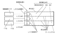
図1は本発明に係る面照明装置の一例を示す断面図、図2はその要部を示す斜視図、図3は散乱凹部を拡大して示す説明図、図4は他の実施形態を示す説明図である。 1 is a cross-sectional view showing an example of a surface illumination device according to the present invention, FIG. 2 is a perspective view showing an essential part thereof, FIG. 3 is an explanatory view showing an enlarged scattering recess, and FIG. 4 shows another embodiment. It is explanatory drawing.
図1〜図3に示す面照明装置1は、正面を発光面2とし、少なくとも一側面をLED装着面3とする透明導光体Bに、発光波長の異なる複数種類のLEDとしてRGB三原色のLED4R、4G、4Bが装着され、各LED4R、4G、4Bからの照射光を導光体B内部で散乱させ、発光面2からその散乱光を均一に出射させるものである。
The surface illumination device 1 shown in FIG. 1 to FIG. 3 has an RGB three
透明導光体Bは、本例では、平面部を発光面5とする透明導光板6R、6G、6Bがその発光面5を正面に向けて三層に積層されて成り、LED装着面3となる各透明導光板6R、6G、6Bの側面にLED装着孔7…が6個ずつ等ピッチで形成されており、赤色LED4R、緑色LED4G及び青色LED4Bが各導光板6R、6G、6Bごとに配列されている。
これにより、発光方向に沿って配列されたLED4R、4G、4Bの発光波長の組み合わせが、各列とも等しく選定されることとなる。
In this example, the transparent light guide B is formed by laminating transparent
Thereby, the combination of the light emission wavelengths of the
各透明導光板6R、6G、6Bの底面8には、各LED4R、4G、4Bから入射された光を散乱させる散乱凹部9…が形成されている。
この散乱凹部9…は、LED装着面3と平行な線状に形成され、且つ、LED装着面3から離れるにしたがってピッチが狭くなるように形成されている。
このように、線状の散乱凹部9…のピッチを変化させることにより、LED装着面3に近い側は散乱光の量を少なくし、LED装着面3から遠くなるにつれて散乱光の量を多くすることにより、発光面5から均一な散乱光が照射させることができる。
On the
The
Thus, by changing the pitch of the
散乱凹部9の形状は任意であるが、V字溝や、図3に示すように、レーザ加工により底面の直径×深さが0.1mm×0.1mmの円錐形状のドット状のピットを0.1mmピッチで連続形成することにより線状に形成されている。
円錐形状のピットを連続形成した場合は、V字溝に比して、LED4R、4G、4Bから入射された光をよりランダムに散乱させることができ、これにより発光面2から照射される光の均一性が向上する。
The shape of the
When the conical pits are continuously formed, the light incident from the
さらに、透明導光体Bは、発光面2及びLED装着面3を開放し、それ以外の面を光散乱板で囲むケーシング10に収納されている。
これにより、発光面2及びLED装着面3以外の面に光散乱板が密着されて、これら各面から外部に出射される散乱光を導光体B内部に反射させ、その一部を照明光として有効利用することができる。
Further, the transparent light guide B is accommodated in a
As a result, the light scattering plate is brought into close contact with a surface other than the
なお、各色LED4R、4G、4Bには、各色ごとにLED4R、4G、4Bを点灯/消灯し、調光する駆動回路11R、11G、11Bが接続され、発光波長ごとに光量をコントロールすることができるようになっている。
Note that the
以上が本発明の一構成例であって、次にその作用について説明する。
面照明装置1は、透明導光体Bが3層に積層された導光板6R、6G、6Bでなり、夫々の底面8に各LED4R、4G、4Bから入射された光を散乱させる散乱凹部9…が形成されているので、各色のLEDから照射された光は散乱凹部9…で散乱され、その一部が導光板6R、6G、6Bの発光面5を通り、導光体Bの発光面2に向かう。
また、導光体Bの発光面2以外の面に達した光は、ケーシング10により導光体B内部に反射され、その一部が照明光として有効利用される。
The above is one configuration example of the present invention, and the operation thereof will be described next.
The surface illumination device 1 includes
Further, the light reaching the surface other than the
そして、単色照明を行う場合は、駆動回路11R、11G、11Bにより、LED4R、4G、4Bのいずれか一色のみを点灯させれば、その光がまず対応する透明導光板6R、6G、6Bの散乱凹部9…や周囲の散乱板で散乱され、その散乱光が導光体Bの発光面3に向かう。
このとき、各色LED4R、4G、4Bは近接させて配列することができるので、RGBのLEDを一列に並べるときのように同色のLEDとの間に3ピッチ分もの間隔が形成されることがなく、輝度ムラを生じないので、均一な単色照明が得られる。
また、一色あたりの素子数を減らすこともないので、輝度が低下することもない。
When performing monochromatic illumination, if only one of the
At this time, since the
Further, since the number of elements per color is not reduced, the luminance is not lowered.
次いで、混色照明を行う場合は、駆動回路11R、11G、11Bにより、LED4R、4G、4Bの任意の2色以上のLEDを点灯すれば、その光がまず対応する透明導光板6R、6G、6Bの散乱凹部9…や周囲の散乱板で散乱され、その散乱光が導光体Bの発光面3に向かう。
各色のLED4R、4G、4Bを配列した導光板6R、6G、6Bは発光方向に対して前後に配設されているので、色ムラを起こすことがなく、発光面3から均一な混色光を出射させることができる。
このとき、必要に応じて各色LED4R、4G、4Bの光量をコントロールすれば、任意の色の照明光を照射することができる。
Next, in the case of performing mixed color illumination, if the LEDs of any two or more of the
The
At this time, if the light quantity of each color LED4R, 4G, 4B is controlled as needed, illumination light of arbitrary colors can be irradiated.
上述の説明では、各色のLED4R、4G、4Bを各導光板6R、6G、6Bごとに個別に装着した場合について説明したが、本発明はこれに限らず、発光方向に沿って配列されたLED4R、4G、4Bの発光波長の組み合わせが各列とも等しければその順序が相違する場合であっても良く、例えば、図4に示すように、三層の導光板6U、6M、6Dのそれぞれに、RGBのLED4R、4G、4Bが発光方向に重ならないように配列してもよい。
また、LEDは二色以上であれば三色に限られるものではなく、さらに、可視光に限らず発光波長が異なるものであれば赤外光や紫外光を発光するものであってもよい。
さらに、駆動回路11R、11G、11Bは、点灯/消灯のみを行い、光量のコントロールを行わないものであっても良い
In the above description, the case where the
Further, the LED is not limited to three colors as long as it has two or more colors, and may emit infrared light or ultraviolet light as long as the emission wavelength is not limited to visible light.
Furthermore, the
さらにまた、高輝度単色照明として使用する場合は、図4において三層(複数層)の導光板6U、6M、6Dのそれぞれに、RGBのLED4R、4G、4Bに替えて、任意の発光色のLED、例えば高輝度白色LEDを配列すれば、単純計算で三倍の輝度の単色照明として使用することができる。
Furthermore, when used as high-intensity monochromatic illumination, each of the three layers (multiple layers) of the
本発明は、透明導光体の内部で光を散乱させ、発光面となる正面側からその散乱光を均一に出射させる面照明装置の用途に適している。 The present invention is suitable for the use of a surface illumination device that scatters light inside a transparent light guide and uniformly emits the scattered light from the front side serving as a light emitting surface.
1 面照明装置
2 発光面
3 LED装着面
B 透明導光体
4R、4G、4B LED
5 発光面
6R、6G、6B 透明導光板
7 LED装着孔
8 底面
9 散乱凹部
10 ケーシング
11R、11G、11B 駆動回路
DESCRIPTION OF SYMBOLS 1
5
Claims (6)
前記透明導光体は、RGB各色のLEDを装着した三層の透明導光板がその発光面を正面に向けて積層されて成り、
前記各透明導光板には、LED装着面となる各導光板の側面に前記LEDが所定ピッチで装着されると共に、発光方向に沿って配列されたLEDの発光波長の組み合わせが、各列とも等しく選定されていることを特徴とする面照明装置。 A plurality of types of LEDs with different emission wavelengths are mounted on a transparent light guide having a front surface as a light emitting surface and at least one side as an LED mounting surface, and the light emitted from each LED is scattered by scattering inside the light guide. In a surface illumination device that emits from a surface,
The transparent light guide is transparent light guide plate of a three-layer equipped with RGB color LED is made is the product layer toward the light emitting surface on the front,
In each of the transparent light guide plates, the LEDs are mounted at a predetermined pitch on the side surface of each light guide plate serving as an LED mounting surface, and the combination of the emission wavelengths of the LEDs arranged along the light emission direction is the same for each column. A surface illumination device that is selected.
Priority Applications (4)
| Application Number | Priority Date | Filing Date | Title |
|---|---|---|---|
| JP2005219815A JP4721803B2 (en) | 2005-07-29 | 2005-07-29 | Surface lighting device |
| TW095124596A TW200716915A (en) | 2005-07-29 | 2006-07-06 | Planar illuminating device |
| KR1020060064827A KR20070014974A (en) | 2005-07-29 | 2006-07-11 | A plane illumination apparatus |
| CNA2006101081514A CN1912457A (en) | 2005-07-29 | 2006-07-28 | Surface lighting device |
Applications Claiming Priority (1)
| Application Number | Priority Date | Filing Date | Title |
|---|---|---|---|
| JP2005219815A JP4721803B2 (en) | 2005-07-29 | 2005-07-29 | Surface lighting device |
Publications (2)
| Publication Number | Publication Date |
|---|---|
| JP2007033347A JP2007033347A (en) | 2007-02-08 |
| JP4721803B2 true JP4721803B2 (en) | 2011-07-13 |
Family
ID=37721467
Family Applications (1)
| Application Number | Title | Priority Date | Filing Date |
|---|---|---|---|
| JP2005219815A Expired - Fee Related JP4721803B2 (en) | 2005-07-29 | 2005-07-29 | Surface lighting device |
Country Status (4)
| Country | Link |
|---|---|
| JP (1) | JP4721803B2 (en) |
| KR (1) | KR20070014974A (en) |
| CN (1) | CN1912457A (en) |
| TW (1) | TW200716915A (en) |
Families Citing this family (14)
| Publication number | Priority date | Publication date | Assignee | Title |
|---|---|---|---|---|
| KR200445445Y1 (en) * | 2007-06-22 | 2009-07-30 | 팀윈 옵토 일렉트로닉스 컴퍼니 리미티드 | Multi-functional LED lamp |
| US7845826B2 (en) * | 2008-01-15 | 2010-12-07 | Skc Haas Display Films Co., Ltd. | Multilayered integrated backlight illumination assembly |
| JP2010190786A (en) * | 2009-02-19 | 2010-09-02 | Takeda Chem Ind Ltd | Method and apparatus for print inspection of solid preparation |
| CN101986020B (en) * | 2009-07-29 | 2012-04-18 | 苏州向隆塑胶有限公司 | Method for eliminating color difference of overlapped backlight modules |
| JP4630945B1 (en) * | 2010-02-19 | 2011-02-09 | 株式会社ヒューテック | Defect inspection equipment |
| CN101986014B (en) * | 2010-11-04 | 2012-06-20 | 友达光电股份有限公司 | Lateral light source module |
| CN103090202B (en) * | 2011-10-27 | 2015-01-14 | 东莞市奥普特自动化科技有限公司 | Shadowless lighting device |
| KR101411460B1 (en) * | 2012-04-03 | 2014-06-27 | 주식회사 노블바이오 | Transilluminator using led |
| CN202837583U (en) * | 2012-05-04 | 2013-03-27 | 深圳安嵘光电产品有限公司 | Combined type light guide plate and illuminating lamp |
| US8896827B2 (en) * | 2012-06-26 | 2014-11-25 | Kla-Tencor Corporation | Diode laser based broad band light sources for wafer inspection tools |
| CN103322763A (en) * | 2013-06-03 | 2013-09-25 | 青岛海尔特种电冰箱有限公司 | Refrigerator lighting device and refrigerator |
| CN107816665B (en) * | 2017-11-02 | 2020-01-07 | 深圳市众铭安科技有限公司 | High-color-gamut blue-green LED backlight module and manufacturing method thereof |
| JP6859962B2 (en) | 2018-01-10 | 2021-04-14 | オムロン株式会社 | Image inspection equipment and lighting equipment |
| CN214425903U (en) * | 2021-02-01 | 2021-10-19 | 漳州立达信光电子科技有限公司 | Panel light |
Citations (7)
| Publication number | Priority date | Publication date | Assignee | Title |
|---|---|---|---|---|
| JPH11125818A (en) * | 1997-10-23 | 1999-05-11 | Hitachi Ltd | Liquid crystal display device |
| JPH11353920A (en) * | 1998-06-05 | 1999-12-24 | Citizen Electronics Co Ltd | Multicolor light emitting surface light source unit |
| JP2003187623A (en) * | 2001-12-18 | 2003-07-04 | Sharp Corp | Lighting device and display device using it |
| JP2004127745A (en) * | 2002-10-03 | 2004-04-22 | Sanyo Electric Co Ltd | Surface light source device |
| JP2004196201A (en) * | 2002-12-20 | 2004-07-15 | Toyoda Gosei Co Ltd | License plate illuminating device |
| JP2005019066A (en) * | 2003-06-24 | 2005-01-20 | Toppan Printing Co Ltd | Photoconductor, illuminating device, and color image display |
| JP2005135760A (en) * | 2003-10-30 | 2005-05-26 | Seiko Instruments Inc | Surface light source device, and display device using the same |
-
2005
- 2005-07-29 JP JP2005219815A patent/JP4721803B2/en not_active Expired - Fee Related
-
2006
- 2006-07-06 TW TW095124596A patent/TW200716915A/en unknown
- 2006-07-11 KR KR1020060064827A patent/KR20070014974A/en not_active Application Discontinuation
- 2006-07-28 CN CNA2006101081514A patent/CN1912457A/en active Pending
Patent Citations (7)
| Publication number | Priority date | Publication date | Assignee | Title |
|---|---|---|---|---|
| JPH11125818A (en) * | 1997-10-23 | 1999-05-11 | Hitachi Ltd | Liquid crystal display device |
| JPH11353920A (en) * | 1998-06-05 | 1999-12-24 | Citizen Electronics Co Ltd | Multicolor light emitting surface light source unit |
| JP2003187623A (en) * | 2001-12-18 | 2003-07-04 | Sharp Corp | Lighting device and display device using it |
| JP2004127745A (en) * | 2002-10-03 | 2004-04-22 | Sanyo Electric Co Ltd | Surface light source device |
| JP2004196201A (en) * | 2002-12-20 | 2004-07-15 | Toyoda Gosei Co Ltd | License plate illuminating device |
| JP2005019066A (en) * | 2003-06-24 | 2005-01-20 | Toppan Printing Co Ltd | Photoconductor, illuminating device, and color image display |
| JP2005135760A (en) * | 2003-10-30 | 2005-05-26 | Seiko Instruments Inc | Surface light source device, and display device using the same |
Also Published As
| Publication number | Publication date |
|---|---|
| CN1912457A (en) | 2007-02-14 |
| TW200716915A (en) | 2007-05-01 |
| JP2007033347A (en) | 2007-02-08 |
| KR20070014974A (en) | 2007-02-01 |
Similar Documents
| Publication | Publication Date | Title |
|---|---|---|
| JP4721803B2 (en) | Surface lighting device | |
| JP2008066032A (en) | Lighting device | |
| KR100708147B1 (en) | Light emitting cluster and direct light type back light unit and liquid display apparatus employing it | |
| KR101166243B1 (en) | Luminous body | |
| CN101517442B (en) | Illumination system, luminaire and display device | |
| JP5515712B2 (en) | Light emitting device | |
| JP5066462B2 (en) | Vehicle lighting | |
| JP2008192395A (en) | Lighting device, and liquid crystal display device | |
| JP2007155791A (en) | Surface light source device | |
| JP2008522378A (en) | Lighting device | |
| JP2008226792A (en) | Planar light source unit | |
| WO2013128771A1 (en) | Lighting module and lighting device provided with same | |
| JPH07270624A (en) | Light transmission plate for surface light emission | |
| TWI553915B (en) | Led device and liquid crystal display having the same | |
| JP4995110B2 (en) | Light source device | |
| EP2492898A2 (en) | Light Emitting Device | |
| JP2008021932A (en) | Light emitting device | |
| JP6136002B2 (en) | Lighting device | |
| JP5416268B1 (en) | High-reflection reflector light source | |
| KR101805918B1 (en) | Lighting apparatus | |
| JP2018056000A (en) | Lighting device | |
| JP4806343B2 (en) | Lighting device | |
| JP2006309985A (en) | Illumination apparatus | |
| KR20100114174A (en) | Led lighting module having reflex composition for activate loss light | |
| KR101204736B1 (en) | Luminescent diode for liquid crystal display device |
Legal Events
| Date | Code | Title | Description |
|---|---|---|---|
| A621 | Written request for application examination |
Free format text: JAPANESE INTERMEDIATE CODE: A621 Effective date: 20080723 |
|
| A977 | Report on retrieval |
Free format text: JAPANESE INTERMEDIATE CODE: A971007 Effective date: 20101125 |
|
| A131 | Notification of reasons for refusal |
Free format text: JAPANESE INTERMEDIATE CODE: A131 Effective date: 20101207 |
|
| A521 | Written amendment |
Free format text: JAPANESE INTERMEDIATE CODE: A523 Effective date: 20110207 |
|
| A01 | Written decision to grant a patent or to grant a registration (utility model) |
Free format text: JAPANESE INTERMEDIATE CODE: A01 Effective date: 20110315 |
|
| A01 | Written decision to grant a patent or to grant a registration (utility model) |
Free format text: JAPANESE INTERMEDIATE CODE: A01 |
|
| A61 | First payment of annual fees (during grant procedure) |
Free format text: JAPANESE INTERMEDIATE CODE: A61 Effective date: 20110405 |
|
| FPAY | Renewal fee payment (event date is renewal date of database) |
Free format text: PAYMENT UNTIL: 20140415 Year of fee payment: 3 |
|
| R150 | Certificate of patent or registration of utility model |
Free format text: JAPANESE INTERMEDIATE CODE: R150 |
|
| S531 | Written request for registration of change of domicile |
Free format text: JAPANESE INTERMEDIATE CODE: R313531 |
|
| S533 | Written request for registration of change of name |
Free format text: JAPANESE INTERMEDIATE CODE: R313533 |
|
| R350 | Written notification of registration of transfer |
Free format text: JAPANESE INTERMEDIATE CODE: R350 |
|
| R250 | Receipt of annual fees |
Free format text: JAPANESE INTERMEDIATE CODE: R250 |
|
| R250 | Receipt of annual fees |
Free format text: JAPANESE INTERMEDIATE CODE: R250 |
|
| S533 | Written request for registration of change of name |
Free format text: JAPANESE INTERMEDIATE CODE: R313533 |
|
| R350 | Written notification of registration of transfer |
Free format text: JAPANESE INTERMEDIATE CODE: R350 |
|
| LAPS | Cancellation because of no payment of annual fees |