JP4715260B2 - Condenser microphone and manufacturing method thereof - Google Patents
Condenser microphone and manufacturing method thereof Download PDFInfo
- Publication number
- JP4715260B2 JP4715260B2 JP2005084455A JP2005084455A JP4715260B2 JP 4715260 B2 JP4715260 B2 JP 4715260B2 JP 2005084455 A JP2005084455 A JP 2005084455A JP 2005084455 A JP2005084455 A JP 2005084455A JP 4715260 B2 JP4715260 B2 JP 4715260B2
- Authority
- JP
- Japan
- Prior art keywords
- electrode
- forming
- sacrificial layer
- etching stopper
- stopper film
- Prior art date
- Legal status (The legal status is an assumption and is not a legal conclusion. Google has not performed a legal analysis and makes no representation as to the accuracy of the status listed.)
- Expired - Fee Related
Links
Images


Description
本発明は、大気に連通する開口を備えたシリコン基板の該開口の上部に第1電極(ダイアフラム)と第2電極(背面板:バックプレート)が空間部を介して相対向するように配置されてコンデンサが形成されたコンデンサマイクロホンおよびその製造方法に関する。 In the present invention, a first electrode (diaphragm) and a second electrode (back plate: back plate) are arranged on top of an opening of a silicon substrate having an opening communicating with the atmosphere so as to face each other through a space portion. The present invention relates to a condenser microphone in which a condenser is formed and a manufacturing method thereof.
従来より、音圧で振動する薄いダイアフラム(第1電極)と、これに近接して平行に形成されたバックプレート(第2電極)とで構成されるコンデンサ型のマイクロホン(コンデンサマイクロホン)が知られている。この種のコンデンサマイクロホンは、ダイアフラム(第1電極)が振動するとコンデンサの容量が変化し、これを電圧に変換して音声信号として取り出すようになされている。このような従来のマイクロホンにあっては、複数種の部品を組み立てて作製するため、主に、次の(1)〜(3)に示されるような種々の問題点があった。 Conventionally, a condenser type microphone (condenser microphone) composed of a thin diaphragm (first electrode) that vibrates with sound pressure and a back plate (second electrode) formed in close proximity to the diaphragm is known. ing. In this type of condenser microphone, when the diaphragm (first electrode) vibrates, the capacitance of the condenser changes, and this is converted into a voltage to be taken out as an audio signal. In such a conventional microphone, since various types of parts are assembled and manufactured, there are mainly various problems as shown in the following (1) to (3).
(1)部品の組立工程の精度の制約により、小型化するのにも限界があることから、携帯電話機等の小型の電子機器に搭載されている半導体部品などの他のモジュールに比べて、厚さや占有面積も大きくなってしまい、回路基板の実装密度を高めることの妨げになっていた。
(2)また、部品の材質が個々に異なって、熱膨張率に差異があることから、実装工程における半田付けなどの複数回の熱処理による熱衝撃で、熱歪みによる変形が生じてしまうということがあった。
(3)さらに、振動膜やスペーサー絶縁部などに樹脂材料からなる部品を採用した場合には、バンプ/リフローなどのように高温処理を伴う実装工程により一括処理することができず、効率化を図ることができなかった。
(1) Since there is a limit to downsizing due to the precision of the assembly process of parts, it is thicker than other modules such as semiconductor parts mounted on small electronic devices such as mobile phones. Further, the occupied area is increased, which hinders increasing the mounting density of the circuit board.
(2) In addition, since the material of each part is different and the coefficient of thermal expansion is different, the thermal shock due to multiple heat treatments such as soldering in the mounting process will cause deformation due to thermal distortion. was there.
(3) Furthermore, when parts made of resin material are used for the vibration film and spacer insulation, etc., it is impossible to perform batch processing by a mounting process involving high-temperature processing such as bump / reflow, thereby improving efficiency. I couldn't plan.
そこで、マイクロマシン技術(MEMS:Micro Electro Mechanical System)を適用して、マイクロホンを小型化することが特許文献1あるいは特許文献2にて提案されるようになった。特許文献1にて提案されたマイクロホンにあっては、基台(シリコン基板)の中央部に音圧により振動する振動膜を形成するとともに、この振動膜の周囲を囲む支持部が背面板を支持して振動膜に対面させることにより、振動膜と背面板との間に支持部を介装して振動膜の振動空間を確保する積層構造に構成するようにしている。これにより、半導体製造技術(マイクロマシン技術)により作製可能でコンデンサ型マイクロホンとして機能するチップマイクロホンが実現できるというものである。この場合、振動膜(ダイアフラム)には貫通孔が形成されておらず、背面板に貫通孔が形成されていて圧力の調整が行われるようになされている。 Thus, Patent Document 1 or Patent Document 2 has proposed that a microphone is miniaturized by applying a micro electro mechanical system (MEMS). In the microphone proposed in Patent Document 1, a vibration film that vibrates due to sound pressure is formed at the center of the base (silicon substrate), and a support portion surrounding the vibration film supports the back plate. Then, by facing the vibration film, a laminated structure that secures a vibration space of the vibration film by interposing a support portion between the vibration film and the back plate is configured. Thus, a chip microphone that can be manufactured by a semiconductor manufacturing technology (micromachine technology) and functions as a condenser microphone can be realized. In this case, no through-hole is formed in the vibration film (diaphragm), and a through-hole is formed in the back plate so that the pressure is adjusted.
また、特許文献2にて提案されたものにあっては、SOI(Silicon On Insulator)基板のボディー・シリコン層の上に形成されたポリシリコンダイヤフラムを有するマイクロメカニカルデバイスとして設計されている。このマイクロメカニカルデバイスにおいては、基板内の裏側にはボディー・シリコン層内の開口を介してダイヤフラムとボディー・シリコン層間の空洞と接続されている空所が存在し、この開口によりダイヤフラムの振動静止時に空洞(チャンバー)内の圧力平衡が生じるようになされている。この場合、SOI基板で構成されたチップ表面からの音圧をダイアフラムで受け、ダイアフラム内で発生する気体の流通および圧力の調整をチップ裏面に形成された空洞(チャンバー)に連通する流通孔を通して行われるようになされている。
ところが、上述した特許文献1にて提案されたマイクロホンにおいては、組立時にチップ表面に空間を形成する必要があるため、組み立て工程が複雑になるという問題を生じた。また、モジュール基板への実装面にキャップによる凹凸があるため、実装工程が複雑になり、製造コストが高くなるという問題を生じた。 However, the microphone proposed in Patent Document 1 described above has a problem in that the assembly process is complicated because it is necessary to form a space on the chip surface during assembly. In addition, since the mounting surface on the module substrate has irregularities due to the cap, the mounting process becomes complicated and the manufacturing cost increases.
一方、上述した特許文献2にて提案されたマイクロホンにおいては、チップ表面に気体の流通孔があるため、チップ表面を樹脂でモールドするプラスチックパッケージやチップ・サイズ・パッケージ(CSP)とのマッチングが悪いという問題が生じた。 On the other hand, in the microphone proposed in Patent Document 2 described above, since there is a gas flow hole on the chip surface, matching with a plastic package or chip size package (CSP) in which the chip surface is molded with resin is poor. The problem that occurred.
そこで、本発明は上記の如き問題点を解消するためになされたものであり、チップ・サイズ・パッケージ(CSP)で容易にコンデンサマイクロホンが製造できる構造にして、超小型のコンデンサマイクロホンを低コストで提供できるようにすることを目的とする。 Accordingly, the present invention has been made to solve the above-described problems, and has a structure in which a capacitor microphone can be easily manufactured with a chip size package (CSP), and an ultra-small capacitor microphone can be manufactured at low cost. The purpose is to be able to provide.
本発明は、大気に連通する開口を備えたシリコン基板の該開口の上部に第1電極と第2電極が空間部を介して対向するように配置されてコンデンサが形成されたコンデンサマイクロホンの製造方法であって、上記目的を達成するため、シリコン基板上にエッチングストッパー膜を成膜するエッチングストッパー膜成膜工程と、エッチングストッパー膜の上にダイヤフラムとなる第1電極を成膜する第1電極成膜工程と、第1電極およびエッチングストッパー膜に所定形状の貫通孔を形成する貫通孔形成工程と、貫通孔が形成された第1電極の上に犠牲層を形成する犠牲層形成工程と、犠牲層の上に背面板(バックプレート)となる第2電極を成膜する第2電極成膜工程と、第2電極の上に犠牲層エッチングストッパー膜を成膜する犠牲層エッチングストッパー膜成膜工程と、シリコン基板に大気に連通する開口を形成する開口形成工程と、第1電極およびエッチングストッパー膜に形成された貫通孔を通して犠牲層を除去する犠牲層除去工程とを備えていることを特徴とする。 The present invention relates to a method of manufacturing a condenser microphone in which a capacitor is formed by arranging a first electrode and a second electrode so as to face each other with a space portion above an opening of a silicon substrate having an opening communicating with the atmosphere. In order to achieve the above object, an etching stopper film forming step for forming an etching stopper film on a silicon substrate and a first electrode component for forming a first electrode serving as a diaphragm on the etching stopper film are formed. A film process; a through-hole forming process for forming a through-hole having a predetermined shape in the first electrode and the etching stopper film; a sacrificial layer forming process for forming a sacrificial layer on the first electrode in which the through-hole is formed; A second electrode film forming step for forming a second electrode to be a back plate on the layer, and a sacrificial layer etch film for forming a sacrificial layer etching stopper film on the second electrode. And a sacrificial layer removing step of removing the sacrificial layer through a through hole formed in the first electrode and the etching stopper film. It is characterized by.
このように、第1電極と第2電極が犠牲層を介して相対向するように形成されており、この犠牲層を第1電極とエッチングストッパー膜に形成された貫通孔を通して除去するだけて、ダイヤフラムとなる第1電極と背面板(バックプレート)となる第2電極が空間部を介して容易に対向させることが可能となる。このため、この種のコンデンサマイクロホンを容易に超小型化することが可能になるとともに、簡単、容易に製造でき、しかも、安価に製造できるようになる。 Thus, the first electrode and the second electrode are formed so as to face each other through the sacrificial layer, and only by removing the sacrificial layer through the through-hole formed in the first electrode and the etching stopper film, The first electrode serving as a diaphragm and the second electrode serving as a back plate (back plate) can be easily opposed to each other through the space portion. For this reason, this type of condenser microphone can be easily miniaturized, can be easily and easily manufactured, and can be manufactured at low cost.
そして、上述のようなコンデンサマイクロホンを製造するには、シリコン基板上にエッチングストッパー膜を成膜するエッチングストッパー膜成膜工程と、エッチングストッパー膜の上にダイヤフラムとなる第1電極を成膜する第1電極成膜工程と、第1電極に所定形状の貫通孔を形成する貫通孔形成工程と、貫通孔が形成された第1電極の上に犠牲層を形成する犠牲層形成工程と、犠牲層の上に背面板となる第2電極を成膜する第2電極成膜工程と、第2電極の上に犠牲層エッチングストッパー膜を成膜する犠牲層エッチングストッパー膜成膜工程と、第2電極と犠牲層エッチングストッパ膜を貫通して大気に連通する気体流通孔を形成する気体流通孔形成工程と、シリコン基板に大気に連通する開口を形成する開口形成工程と、シリコン基板に形成された開口の上部に存在するエッチングストッパー膜を除去するとともに、第1電極に形成された貫通孔および第2電極と犠牲層エッチングストッパ膜に形成された気体流通孔を通して犠牲層を除去する犠牲層除去工程とを備えるようにすればよい。 In order to manufacture the condenser microphone as described above, an etching stopper film forming step for forming an etching stopper film on a silicon substrate, and a first electrode that forms a diaphragm on the etching stopper film are formed. A one-electrode film forming step, a through-hole forming step for forming a through-hole having a predetermined shape in the first electrode, a sacrificial layer forming step for forming a sacrificial layer on the first electrode in which the through-hole is formed, and a sacrificial layer A second electrode film forming step for forming a second electrode serving as a back plate on the substrate, a sacrificial layer etching stopper film forming step for forming a sacrificial layer etching stopper film on the second electrode, and a second electrode A gas flow hole forming step that forms a gas flow hole that passes through the sacrificial layer etching stopper film and communicates with the atmosphere, an opening formation step that forms an opening that communicates with the atmosphere in the silicon substrate, and silicon The etching stopper film existing above the opening formed in the plate is removed, and the sacrificial layer is removed through the through hole formed in the first electrode and the gas flow hole formed in the second electrode and the sacrificial layer etching stopper film. And a sacrificial layer removing step.
このように、第1電極と第2電極が犠牲層を間にして形成されており、この犠牲層を第1電極に形成された貫通孔および第2電極と犠牲層エッチングストッパ膜に形成された気体流通孔を通して除去するだけて、ダイヤフラムとなる第1電極と背面板(バックプレート)となる第2電極が空間部を介して容易に対向させることが可能となる。このため、この種のコンデンサマイクロホンを容易に超小型化することが可能になるとともに、簡単、容易に製造でき、しかも、安価に製造できるようになる。 Thus, the first electrode and the second electrode are formed with the sacrificial layer in between, and the sacrificial layer is formed in the through hole formed in the first electrode and the second electrode and the sacrificial layer etching stopper film. Only by removing through the gas flow hole, the first electrode serving as a diaphragm and the second electrode serving as a back plate (back plate) can be easily opposed to each other through the space portion. For this reason, this type of condenser microphone can be easily miniaturized, can be easily and easily manufactured, and can be manufactured at low cost.
以下に、本発明のコンデンサマイクロホンの実施の形態を、実施例1のコンデンサマイクロホンおよび実施例2のコンデンサマイクロホンとして図1〜図27に基づいて説明するが、本発明はこれらの実施例に何ら限定されるものでなく、本発明の目的を変更しない範囲で適宜変更して実施することが可能である。なお、図1は実施例1のコンデンサマイクロホンの要部を模式的に示す断面図であり、図2〜図13はその製造工程を模式的に示す断面図である。また、図14は実施例2のコンデンサマイクロホンの要部を模式的に示す断面図であり、図15〜図27はその製造工程を模式的に示す断面図である。 Hereinafter, embodiments of the condenser microphone of the present invention will be described as a condenser microphone of Example 1 and a condenser microphone of Example 2 , with reference to FIGS . 1 to 27. However, the present invention is not limited to these Examples. However, the present invention can be implemented with appropriate modifications without departing from the object of the present invention. FIG. 1 is a cross-sectional view schematically showing the main part of the condenser microphone of the first embodiment, and FIGS. 2 to 13 are cross-sectional views schematically showing the manufacturing process. Further, FIG. 14 is a sectional view showing a main portion of the condenser microphone of the second embodiment schematically, FIG. 15 to 27 show Ru sectional view showing the manufacturing steps schematically.
1.実施例1
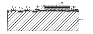
本実施例1のコンデンサマイクロホン10は、図1に示すように、シリコン基板(シリコンウェハ)11の略中央部に形成された開口11aを備え、この開口11aの上部に、ポリシリコンからなる第1電極12と、ポリシリコンからなる第2電極13が空間部14を介して対向するように配置されている。このように空間部14を介して第1電極12と第2電極13が対向することによりコンデンサが形成され、コンデンサ型マイクロホンとして機能するようになされている。
1. Example 1
As shown in FIG. 1, the
ここで、ポリシリコンからなる第1電極12は音圧に応答して第2電極13に対して移動可能なダイヤフラムとして作用する。そして、この第1電極12の開口11a側の表面には、シリコン窒化膜からなるエッチングストッパ膜12aが残存していて、これらの第1電極12とエッチングストッパ膜12aを貫通して開口11aに連通する貫通孔12bが形成されている。一方、ポリシリコンからなる第2電極13は第1電極12に対する背面板(バックプレート)として作用する。そして、この第2電極13の第1電極12に対向する面の反対側には、シリコン窒化膜からなる犠牲層エッチングストッパ膜13aが残存している。
Here, the
なお、第1電極12の一端部はメタル配線16aに接続されているとともに、第2電極13の一端部はメタル配線16bに接続されている。そして、第2電極(背面板)13を覆うように、シリコン酸化膜からなる層間絶縁膜15が形成されている。また、層間絶縁膜15を覆うとともに、メタル配線16a、16bを覆うようにチップ保護膜(酸化膜と窒化膜からなる積層膜)16が形成されている。これらの上部はCSP(チップ・サイズ・パッケージ)を形成した封止樹脂(エポキシ樹脂)17により被覆されている。この場合、封止樹脂17の上部にはんだバンプ(突起電極)19が形成されており、このはんだバンプ19はポスト18aを介して再配線層18に接続されており、この再配線層18はメタル配線16aのいずれかに接続されている。なお、はんだバンプ19は図示しない回路基板にフリップチップ接続されるようになされている。
One end of the
次に、上述のような構成となる実施例1のコンデンサマイクロホン10の半導体製造技術による作製手順(製造工程)を、図2〜図13を用いて以下に説明する。まず、図2に示すように、素子間分離層(フィールド酸化膜)11xやマイクロホンの周辺回路となるウェル、ソース、ドレンなどからなるトランジスタ11yがCMOS半導体製造プロセスにより形成されたシリコン基板(シリコンウェハ)11を用意する。ついで、図3に示すように、この全面にレジスト12cを塗布し、このレジスト12cをダイアフラム形成部(第1電極)12の形状にパターニングした後、レジスト12cをマスクにしてダイアフラム形成部(第1電極)12のフィールド酸化膜11xをエッチングする。
Next, a manufacturing procedure (manufacturing process) of the
ついで、図4に示すように、レジスト12cを除去した後、この全面にエッチングストッパ膜12aとなるシリコン窒化膜をLPCVD(Low Pressure Chemical Vapor Deposition:減圧化学気相成長)法により堆積させる。ついで、この全面に第1電極(ダイアフラム)12となるポリシリコン膜を成膜する。ついで、この上にレジスト12dを塗布して、所定の第1電極(ダイアフラム)12の形状および所定の貫通孔の形状にパターニングする。ついで、図5に示すように、パターニングされたレジスト12dをマスクにしてレジスト12dおよびポリシリコン膜からなる第1電極(ダイアフラム)12をエッチングした後、レジスト12dを除去する。これにより、第1電極(ダイアフラム)12に貫通孔12bが形成されることとなる。
Next, as shown in FIG. 4, after removing the resist 12c, a silicon nitride film to be an
ついで、この全面にレジスト12eを塗布し、このレジスト12eを第1電極(ダイアフラム)12より小さめの形状にパターニングした後、レジスト12eと第1電極(ダイアフラム)12をマスクにして、貫通孔12bの下部のシリコン窒化膜からなるエッチングストッパ膜12aをフロロカーボン系ガス(例えば、CF4,CHF4等)を用いてエッチングする。これにより、図6に示すように、第1電極(ダイアフラム)12に形成された貫通孔12bはエッチングストッパ膜12aを貫通してシリコン基板11の表面に到達することとなる。ついで、レジスト12eを除去した後、この全面に犠牲膜14aとなるシリコン酸化膜と、第2電極(背面板)13となるポリシリコン膜を成膜した後、レジスト13bを塗布して、所定の第2電極(背面板)13の形状にパターニングする。
Next, a resist 12e is applied to the entire surface, and the resist 12e is patterned into a shape smaller than the first electrode (diaphragm) 12, and then the resist 12e and the first electrode (diaphragm) 12 are used as a mask to form the through
この後、図7に示すように、レジスト13bをマスクにしてポリシリコン膜からなる第2電極(背面板)13およびシリコン酸化膜からなる犠牲膜14aを所定の形状にエッチングした。このエッチングにおいては、まず、Cl2とO2の混合ガスを用いてポリシリコン膜からなる第2電極(背面板)13のエッチングを行った後、フロロカーボン系ガス(例えば、CF4,CHF4等)を用いてシリコン酸化膜からなる犠牲膜14aのエッチングを行った。ついで、レジスト13bを除去した後、図8に示すように、この全面にエッチングストッパ膜13aとなるシリコン窒化膜をLPCVD法により堆積させる。ついで、図9に示すように、これらの上に層間絶縁膜15,メタル配線16a,16bおよびチップ保護膜16を周知のCMOS半導体製造技術により形成する。
Thereafter, as shown in FIG. 7, the second electrode (back plate) 13 made of a polysilicon film and the
ついで、CSP(Chip Size Package)工程において、図10に示すように、これらの全面にパッケージとなる封止樹脂層(エポキシ樹脂)17を被覆させた。この場合、封止樹脂層17の一部に銅(Cu)からなるポスト18aが埋設され、かつ、このポスト18aとメタル配線16aの一部とが接続されるように銅(Cu)からなる再配線層18が形成されるようにした。
Then, in a CSP (Chip Size Package) process, as shown in FIG. 10, a sealing resin layer (epoxy resin) 17 serving as a package was coated on the entire surface. In this case, a
ついで、図11に示すように、基板11の裏面の全面に開口11a形成用のマスク11bを形成するとともに、基板11の表面の全面にも封止樹脂層17の保護用のマスク17aを形成する。この場合、マスク11b,17aの材質としては、レジスト層、アルミニウム膜、シリコン酸化膜、シリコン窒化膜などから選択するようにすればよい。この後、基板11の裏面をDeepRIE(Deep Reactive Ion Etching)、TMAH(Tetramethyl ammonium hydroxide)やKOHを用いてエッチングして、基板11の裏面に開口11aを形成した。なお、このエッチングにおいて、開口11aの深さ(高さ)がシリコン窒化膜からなるエッチングストッパ膜12aまでとなるように行われる。
Next, as shown in FIG. 11, a
ついで、基板11の表裏面に形成されたマスク11b,17aを除去した後、図12に示すように、この表面に封止樹脂層17の保護用のマスク17bを形成する。この場合、マスク17bの材質としては、レジスト層、アルミニウム膜、シリコン窒化膜などから選択するようにすればよい。この後、フッ酸(例えば、63BHF、希釈HF、ストレートHFなど)に浸漬してフッ酸処理を行い、第1電極(ダイアフラム)12と第2電極(背面板)13との間に形成されてシリコン酸化膜からなる犠牲膜14aを除去した。このフッ酸処理において、処理液は貫通孔12bを通して犠牲膜14a内に流入することとなる。これにより、第1電極(ダイアフラム)12と第2電極(背面板)13との間に貫通孔12bを通して開口11aに連通する空間部14が形成されることとなる。
Next, after removing the
ついで、マスク17bを除去した後、封止樹脂層17に埋設するように形成されたポスト18aにはんだバンプ19(図1参照)を固着する。このようにして基板11にマイク領域Aを形成した後、図13に示すように、ダイジングブレードBにより各マイク領域A毎にダイジングする。これにより、図1に示すように、CSPの表面にマイクロホンが形成されたチップ、即ち、コンデンサマイクロホン10が形成されることとなる。
Next, after removing the
上述したように、本実施例1のコンデンサマイクロホン10は、背面板(バックプレート)となる第2電極13に対向する第1電極12と、この上に形成されたエッチングストッパ膜12aに大気に連通する貫通孔12bが形成されているので、音圧が第1電極12に作用した際に第1電極12と第2電極13で形成される空間部14に存在する空気が、当該貫通孔12bより大気に連通する開口11a内に排気されるようになる。これにより、第1電極12は第2電極13に対して敏感に移動可能なダイヤフラムとなって、音圧に敏感に応答することができるようになり、感度の優れたコンデンサマイクロホンとなる。また、第1電極12の開口11a側の表面にエッチングストッパ膜12aが残存しているので、このエッチングストッパ膜12aは第1電極12の強度を補強するように作用し、この種のコンデンサマイクロホンの耐久性が向上する。
As described above, the
この場合、第1電極12と第2電極13の間に犠牲層14aを形成しておき、この犠牲層14aを第1電極12とエッチングストッパー膜12aに形成された貫通孔12bを通して除去するだけて、ダイヤフラムとなる第1電極12と背面板(バックプレート)となる第2電極13が空間部14を介して容易に対向させることが可能となる。このため、この種のコンデンサマイクロホンを容易に超小型化することが可能になるとともに、簡単、容易に製造でき、しかも、安価に製造できるようになる。
In this case, a
2.実施例2
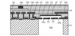
ついで、実施例2のマイクロホンについて、図14に基づいて以下に説明する。本実施例2のマイクロホン30は、図14に示すように、シリコン基板(シリコンウェハ)31の略中央部に形成された大気に連通する開口31aを備え、この開口31aの上部に、ポリシリコンからなる第1電極32と、ポリシリコンからなる第2電極33が空間部34を介して対向するように配置されている。このように空間部34を介して第1電極32と第2電極33が対向することによりコンデンサが形成され、コンデンサ型マイクロホンとして機能するようになされている。
2. Example 2
Then, the microphone of the second embodiment will be described below with reference to FIG. 14. As shown in FIG. 14 , the
ここで、ポリシリコンからなる第1電極32は音圧に応答して第2電極33に対して移動可能なダイヤフラムとして作用する。そして、この第1電極32の開口31a側の表面には、シリコン窒化膜からなるエッチングストッパ膜32aは残存しないようになされている。一方、ポリシリコンからなる第2電極33は第1電極32に対する背面板(バックプレート)として作用する。そして、この第2電極33の第1電極32に対向する面の反対側には、シリコン窒化膜からなる犠牲層エッチングストッパ膜33aが残存していて、これらの第2電極33とエッチングストッパ膜33aと後述するチップ保護膜(酸化膜と窒化膜からなる積層膜)36を貫通して大気に連通する気体流通孔34aが形成されている。
Here, the
なお、第1電極32の一端部はメタル配線36aに接続されているとともに、第2電極33の一端部はメタル配線36bに接続されている。そして、第2電極(背面板)33を覆うように、シリコン酸化膜からなる層間絶縁膜35が形成されている。また、層間絶縁膜35を覆うとともに、メタル配線36a、36bを覆うようにチップ保護膜(酸化膜と窒化膜からなる積層膜)36が形成されている。これらの上部はCSP(チップ・サイズ・パッケージ)を形成した封止樹脂(エポキシ樹脂)37により被覆されている。この場合、封止樹脂37の上部にはんだバンプ39が形成されており、このはんだバンプ39はポスト38aを介して再配線層38に接続されており、この再配線層38はメタル配線36aのいずれかに接続されている。なお、はんだバンプ39は図示しない回路基板にフリップチップ接続されるようになされている。
One end of the
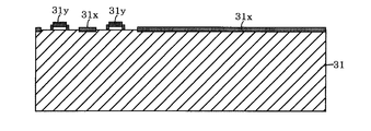
次に、上述のような構成となる実施例2のコンデンサマイクロホン30の半導体製造技術による作製手順(製造工程)を、図15〜図27に基づいて以下に説明する。まず、図15に示すように、素子間分離層(フィールド酸化膜)31xやマイクロホンの周辺回路となるウェル、ソース、ドレンなどからなるトランジスタ31yがCMOS半導体製造プロセスにより形成されたシリコン基板(シリコンウェハ)31を用意する。ついで、図16に示すように、この全面にレジスト32cを塗布し、このレジスト32cをダイアフラム形成部(第1電極)32の形状にパターニングした後、レジスト32cをマスクにしてダイアフラム形成部(第1電極)32のフィールド酸化膜31xをエッチングする。
Next, a description production procedure by the semiconductor manufacturing technology of the
ついで、図17に示すように、レジスト32cを除去した後、この全面にエッチングストッパ膜32aとなるシリコン窒化膜をLPCVD(Low Pressure Chemical Vapor Deposition:減圧化学気相成長)法により堆積させる。ついで、この全面に第1電極(ダイアフラム)32となるポリシリコン膜を成膜する。ついで、この上にレジスト32dを塗布して、所定の第1電極(ダイアフラム)32の形状および所定の貫通孔32bの形状にパターニングする。ついで、図18に示すように、パターニングされたレジスト32dをマスクにしてポリシリコン膜からなる第1電極(ダイアフラム)32をエッチングした後、レジスト32dを除去する。これにより、第1電極(ダイアフラム)32に気体流通孔32bが形成されることとなる。
Next, as shown in FIG. 17 , after removing the resist 32c, a silicon nitride film to be an
ついで、この全面に犠牲膜34bとなるシリコン酸化膜と、第2電極(背面板)33となるポリシリコン膜を成膜した後、レジスト33bを塗布して、所定の第2電極(背面板)33の形状にパターニングする。この後、図19に示すように、レジスト33bをマスクにしてポリシリコン膜からなる第2電極(背面板)33およびシリコン酸化膜からなる犠牲膜34bを所定の形状にエッチングした。ついで、レジスト33bを除去した後、図20に示すように、この全面にエッチングストッパ膜33aとなるシリコン窒化膜をLPCVD法により堆積させる。ついで、図21に示すように、これらの上に層間絶縁膜35,メタル配線36a,36bおよびチップ保護膜36を周知のCMOS半導体製造技術により形成する。
Next, after a silicon oxide film to be the
ついで、この上にレジスト37aを塗布して、後述する気体流通孔34aの形状にパターニングする。ついで、図22に示すように、パターニングされたレジスト37aをマスクにしてチップ保護膜36、シリコン窒化膜からなるエッチングストッパ膜33aおよび第2電極(背面板)33をエッチングする。この後、レジスト37aを除去することにより、チップ保護膜36、エッチングストッパ膜33aおよび第2電極(背面板)33に気体流通孔34aが形成されることとなる。
Next, a resist 37a is applied thereon and patterned into the shape of a
ついで、CSP(Chip Size Package)工程において、図23に示すように、これらの全面にパッケージとなる封止樹脂層(エポキシ樹脂)37を被覆させた。この場合、封止樹脂層37の一部に銅(Cu)からなるポスト38aが埋設され、かつ、このポスト38aとメタル配線36aの一部とが接続されるように銅(Cu)からなる再配線層38が形成されるようにした。
Then, in a CSP (Chip Size Package) process, as shown in FIG. 23 , a sealing resin layer (epoxy resin) 37 serving as a package was coated on the entire surface. In this case, a
この後、基板31の表面に第2電極(背面板)33の上部に形成される開口37cの形状に一致するマスク37bをレジストにより形成する。ついで、図24に示すように、DeepRIE(Deep Reactive Ion Etching)、TMAH(Tetramethyl ammonium hydroxide)やKOHを用いて封止樹脂層37をエッチングして、第2電極(背面板)33の上部の封止樹脂層層37に開口37cを形成するとともに、チップ保護膜36に気体流通孔34aを形成した。
Thereafter, a
ついで、基板31の裏面の全面に開口31a形成用のシリコン酸化膜からなるマスク31bを形成する。この場合、マスク31bの材質としては、レジスト層、アルミニウム膜、シリコン酸化膜、シリコン窒化膜などから選択するようにすればよい。この後、基板31の裏面をDeepRIE(Deep Reactive Ion Etching)、TMAH(Tetramethyl ammonium hydroxide)やKOHを用いてエッチングして、図25に示すように、基板31の裏面に開口31aを形成した。なお、このエッチングにおいて、開口31aの深さ(高さ)がシリコン酸化膜からなるエッチングストッパ膜32aまでとなるように行われる。
Next, a
ついで、基板31の裏面に形成されたマスク31bを除去した後、フッ酸(例えば、63BHF、希釈HF、ストレートHFなど)に浸漬してフッ酸処理を行い、開口31aの上部に存在するシリコン酸化膜からなるエッチングストッパ膜32aを除去するとともに、第1電極(ダイアフラム)32と第2電極(背面板)33との間に形成されてシリコン酸化膜からなる犠牲膜34aを除去する。これにより、図26に示すように、第1電極(ダイアフラム)32と第2電極(背面板)33との間に気体流通孔34aを通して開口37cに連通するとともに、貫通孔32bを通して開口31aに連通する空間部34が形成されることとなる。
Next, after removing the
ついで、マスク37bを除去した後、図14に示すように、封止樹脂層37に埋設するように形成されたポスト38aにはんだバンプ39を固着する。このようにして基板31にマイク領域Cを形成した後、図27に示すように、ダイジングブレードBにより各マイク領域A毎にダイジングする。これにより、図14に示すように、CSPの表面にマイクロホンが形成されたチップ、即ち、コンデンサマイクロホン30が形成されることとなる。
Next, after removing the
上述したように、本実施例2のコンデンサマイクロホン30は、開口31aに連通する貫通孔32bが第1電極32に形成されているとともに、第2電極33と犠牲層エッチングストッパ膜33aを貫通して大気に連通する気体流通孔34aが形成されているので、音圧が第1電極32に作用した際に第1電極32と第2電極33で形成される空間部34に存在する空気が、当該貫通孔32bおよび気体流通孔34aより大気中に排気されるようになる。これにより、第1電極32は第2電極33に対してさらに敏感に移動可能なダイヤフラムとなって、音圧にさらに敏感に応答することができるようになり、さらに感度の優れたコンデンサマイクロホンとなる。
As described above, in the
この場合、第1電極32と第2電極33が犠牲層34bを間にして形成されており、この犠牲層34bを第1電極32に形成された貫通孔32b、および第2電極33と犠牲層エッチングストッパ膜33aに形成された気体流通孔34aを通して除去するだけで、ダイヤフラムとなる第1電極32と背面板(バックプレート)となる第2電極33が空間部34を介して容易に対向させることが可能となる。このため、この種のコンデンサマイクロホンを容易に超小型化することが可能になるとともに、簡単、容易に製造でき、しかも、安価に製造できるようになる。
In this case, the
なお、上述した実施形態においては、チップ保護膜(16,36)として酸化膜と窒化膜からなる積層膜を用いる例について説明したが、これらの上にさらにポリイミド膜を形成するようにしてもよい。また、上述した実施形態においては、封止樹脂層(17,37)を形成する樹脂としてエポキシ樹脂を用いる例について説明したが、エポキシ樹脂に代えてポリイミド樹脂を用いるようにしてもよい。 In the above-described embodiment, the example in which the laminated film composed of the oxide film and the nitride film is used as the chip protective film ( 16, 36 ) has been described. However, a polyimide film may be further formed thereon. . In the embodiment described above, an example in which an epoxy resin is used as the resin for forming the sealing resin layer ( 17, 37 ) has been described. However, a polyimide resin may be used instead of the epoxy resin.
10…マイクロホン、11…シリコン基板(シリコンウェハ)、11a…開口、11x…フィールド酸化膜、11y…トランジスタ、12…第1電極、12a…エッチングストッパ膜、12b…貫通孔、12c…レジスト、12d…レジスト、12e…レジスト、13…第2電極、13a…エッチングストッパ膜、13a…犠牲層エッチングストッパ膜、13b…レジスト、14…空間部、14a…犠牲層(犠牲膜)、15…層間絶縁膜、16…チップ保護膜、16a…メタル配線、16b…メタル配線、17…封止樹脂層、17a…マスク、17b…マスク、18…再配線層、18a…ポスト、19…はんだバンプ、30…マイクロホン、31…シリコン基板(シリコンウェハ)、31a…開口、31b…マスク、31x…フィールド酸化膜、31y…トランジスタ、32…第1電極、32a…エッチングストッパ膜、32b…貫通孔、32c…レジスト、32d…レジスト、33…第1電極、33a…犠牲層エッチングストッパ膜、33b…レジスト、34…空間部、34a…気体流通孔、34b…犠牲層(犠牲膜)、35…層間絶縁膜、36…チップ保護膜、36a…メタル配線、36b…メタル配線、37…封止樹脂層、37a…レジスト、37b…マスク、37c…開口、38…再配線層、38a…ポスト、39…はんだバンプ
DESCRIPTION OF
Claims (4)
前記シリコン基板上にエッチングストッパー膜を成膜するエッチングストッパー膜成膜工程と、
前記エッチングストッパー膜の上にダイヤフラムとなる第1電極を成膜する第1電極成膜工程と、
前記第1電極および前記エッチングストッパー膜に所定形状の貫通孔を形成する貫通孔形成工程と、
前記貫通孔が形成された第1電極の上に犠牲層を形成する犠牲層形成工程と、
前記犠牲層の上に背面板となる第2電極を成膜する第2電極成膜工程と、
前記第2電極の上に犠牲層エッチングストッパー膜を成膜する犠牲層エッチングストッパー膜成膜工程と、
前記シリコン基板に大気に連通する開口を形成する開口形成工程と、
前記第1電極および前記エッチングストッパー膜に形成された貫通孔を通して前記犠牲層を除去する犠牲層除去工程とを備えたことを特徴とするコンデンサマイクロホンの製造方法。 A capacitor in which a first electrode is formed on an upper part of an opening of a silicon substrate having an opening communicating with the atmosphere, and a capacitor is formed by arranging the second electrode on the upper part so as to face each other through a space. A method of manufacturing a microphone,
An etching stopper film forming step of forming an etching stopper film on the silicon substrate;
A first electrode film forming step of forming a first electrode serving as a diaphragm on the etching stopper film;
A through hole forming step of forming a through hole having a predetermined shape in the first electrode and the etching stopper film;
A sacrificial layer forming step of forming a sacrificial layer on the first electrode in which the through hole is formed;
A second electrode film forming step of forming a second electrode serving as a back plate on the sacrificial layer;
A sacrificial layer etching stopper film forming step of forming a sacrificial layer etching stopper film on the second electrode;
An opening forming step of forming an opening communicating with the atmosphere in the silicon substrate;
And a sacrificial layer removing step of removing the sacrificial layer through a through-hole formed in the first electrode and the etching stopper film.
前記シリコン基板上にエッチングストッパー膜を成膜するエッチングストッパー膜成膜工程と、
前記エッチングストッパー膜の上にダイヤフラムとなる第1電極を成膜する第1電極成膜工程と、
前記第1電極および前記エッチングストッパー膜に所定形状の貫通孔を形成する貫通孔形成工程と、
前記貫通孔が形成された第1電極の上に犠牲層を形成する犠牲層形成工程と、
前記犠牲層の上に背面板となる第2電極を成膜する第2電極成膜工程と、
前記第2電極の上に犠牲層エッチングストッパー膜を成膜する犠牲層エッチングストッパー膜成膜工程と、
前記シリコン基板に大気に連通する開口を形成する開口形成工程と、
前記第1電極および前記エッチングストッパー膜に形成された貫通孔を通して前記犠牲層を除去する犠牲層除去工程とを備え、
前記シリコン基板上に前記第1電極、前記第2電極と接続するバンプが形成されていることを特徴とするチップ・サイズ・パッケージの製造方法。 A chip in which a first electrode is formed on an upper portion of an opening of a silicon substrate having an opening communicating with the atmosphere, and a capacitor is formed by placing the second electrode on the upper portion so as to face each other through a space. A size / package manufacturing method,
An etching stopper film forming step of forming an etching stopper film on the silicon substrate;
A first electrode film forming step of forming a first electrode serving as a diaphragm on the etching stopper film;
A through hole forming step of forming a through hole having a predetermined shape in the first electrode and the etching stopper film;
A sacrificial layer forming step of forming a sacrificial layer on the first electrode in which the through hole is formed;
A second electrode film forming step of forming a second electrode serving as a back plate on the sacrificial layer;
A sacrificial layer etching stopper film forming step of forming a sacrificial layer etching stopper film on the second electrode;
An opening forming step of forming an opening communicating with the atmosphere in the silicon substrate;
A sacrificial layer removing step of removing the sacrificial layer through a through hole formed in the first electrode and the etching stopper film,
A method of manufacturing a chip size package , wherein bumps connected to the first electrode and the second electrode are formed on the silicon substrate .
前記シリコン基板上にエッチングストッパー膜を成膜するエッチングストッパー膜成膜工程と、
前記エッチングストッパー膜の上にダイヤフラムとなる第1電極を成膜する第1電極成膜工程と、
前記第1電極に所定形状の貫通孔を形成する貫通孔形成工程と、
前記貫通孔が形成された第1電極の上に犠牲層を形成する犠牲層形成工程と、
前記犠牲層の上に背面板となる第2電極を成膜する第2電極成膜工程と、
前記第2電極の上に犠牲層エッチングストッパー膜を成膜する犠牲層エッチングストッパー膜成膜工程と、
前記第2電極と前記犠牲層エッチングストッパ膜を貫通して大気に連通する気体流通孔を形成する気体流通孔形成工程と、
前記シリコン基板に大気に連通する開口を形成する開口形成工程と、
前記シリコン基板に形成された前記開口の上部に存在する前記エッチングストッパー膜を除去するとともに、前記第1電極に形成された貫通孔および前記第2電極と前記犠牲層エッチングストッパ膜に形成された気体流通孔を通して前記犠牲層を除去する犠牲層除去工程とを備えたことを特徴とするコンデンサマイクロホンの製造方法。 A capacitor in which a first electrode is formed on an upper part of an opening of a silicon substrate having an opening communicating with the atmosphere, and a capacitor is formed by arranging the second electrode on the upper part so as to face each other through a space. A method of manufacturing a microphone,
An etching stopper film forming step of forming an etching stopper film on the silicon substrate;
A first electrode film forming step of forming a first electrode serving as a diaphragm on the etching stopper film;
A through hole forming step of forming a through hole of a predetermined shape in the first electrode;
A sacrificial layer forming step of forming a sacrificial layer on the first electrode in which the through hole is formed;
A second electrode film forming step of forming a second electrode serving as a back plate on the sacrificial layer;
A sacrificial layer etching stopper film forming step of forming a sacrificial layer etching stopper film on the second electrode;
A gas circulation hole forming step of forming a gas circulation hole penetrating the second electrode and the sacrificial layer etching stopper film and communicating with the atmosphere;
An opening forming step of forming an opening communicating with the atmosphere in the silicon substrate;
The etching stopper film existing above the opening formed in the silicon substrate is removed, and the through hole formed in the first electrode and the gas formed in the second electrode and the sacrificial layer etching stopper film are removed. And a sacrificial layer removing step of removing the sacrificial layer through the flow hole.
前記シリコン基板上にエッチングストッパー膜を成膜するエッチングストッパー膜成膜工程と、
前記エッチングストッパー膜の上にダイヤフラムとなる第1電極を成膜する第1電極成膜工程と、
前記第1電極に所定形状の貫通孔を形成する貫通孔形成工程と、
前記貫通孔が形成された第1電極の上に犠牲層を形成する犠牲層形成工程と、
前記犠牲層の上に背面板となる第2電極を成膜する第2電極成膜工程と、
前記第2電極の上に犠牲層エッチングストッパー膜を成膜する犠牲層エッチングストッパー膜成膜工程と、
前記第2電極と前記犠牲層エッチングストッパ膜を貫通して大気に連通する気体流通孔を形成する気体流通孔形成工程と、
前記シリコン基板に大気に連通する開口を形成する開口形成工程と、
前記シリコン基板に形成された前記開口の上部に存在する前記エッチングストッパー膜を除去するとともに、前記第1電極に形成された貫通孔および前記第2電極と前記犠牲層エッチングストッパ膜に形成された気体流通孔を通して前記犠牲層を除去する犠牲層除去工程とを備え、
前記シリコン基板上に前記第1電極、前記第2電極と接続するバンプが形成されていることを特徴とするチップ・サイズ・パッケージの製造方法。 A chip in which a first electrode is formed on an upper portion of an opening of a silicon substrate having an opening communicating with the atmosphere, and a capacitor is formed by placing the second electrode on the upper portion so as to face each other through a space. A size / package manufacturing method,
An etching stopper film forming step of forming an etching stopper film on the silicon substrate;
A first electrode film forming step of forming a first electrode serving as a diaphragm on the etching stopper film;
A through hole forming step of forming a through hole of a predetermined shape in the first electrode;
A sacrificial layer forming step of forming a sacrificial layer on the first electrode in which the through hole is formed;
A second electrode film forming step of forming a second electrode serving as a back plate on the sacrificial layer;
A sacrificial layer etching stopper film forming step of forming a sacrificial layer etching stopper film on the second electrode;
A gas circulation hole forming step of forming a gas circulation hole penetrating the second electrode and the sacrificial layer etching stopper film and communicating with the atmosphere;
An opening forming step of forming an opening communicating with the atmosphere in the silicon substrate;
The etching stopper film existing above the opening formed in the silicon substrate is removed, and the through hole formed in the first electrode and the gas formed in the second electrode and the sacrificial layer etching stopper film are removed. A sacrificial layer removing step of removing the sacrificial layer through the flow hole,
A method of manufacturing a chip size package , wherein bumps connected to the first electrode and the second electrode are formed on the silicon substrate .
Priority Applications (1)
| Application Number | Priority Date | Filing Date | Title |
|---|---|---|---|
| JP2005084455A JP4715260B2 (en) | 2005-03-23 | 2005-03-23 | Condenser microphone and manufacturing method thereof |
Applications Claiming Priority (1)
| Application Number | Priority Date | Filing Date | Title |
|---|---|---|---|
| JP2005084455A JP4715260B2 (en) | 2005-03-23 | 2005-03-23 | Condenser microphone and manufacturing method thereof |
Publications (2)
| Publication Number | Publication Date |
|---|---|
| JP2006270408A JP2006270408A (en) | 2006-10-05 |
| JP4715260B2 true JP4715260B2 (en) | 2011-07-06 |
Family
ID=37205910
Family Applications (1)
| Application Number | Title | Priority Date | Filing Date |
|---|---|---|---|
| JP2005084455A Expired - Fee Related JP4715260B2 (en) | 2005-03-23 | 2005-03-23 | Condenser microphone and manufacturing method thereof |
Country Status (1)
| Country | Link |
|---|---|
| JP (1) | JP4715260B2 (en) |
Families Citing this family (5)
| Publication number | Priority date | Publication date | Assignee | Title |
|---|---|---|---|---|
| JP5016449B2 (en) | 2007-11-13 | 2012-09-05 | ローム株式会社 | Semiconductor device |
| JP5374716B2 (en) * | 2008-03-18 | 2013-12-25 | エプコス アクチエンゲゼルシャフト | Microphone and manufacturing method thereof |
| KR101065292B1 (en) | 2008-12-22 | 2011-09-19 | 한국전자통신연구원 | The mems microphone and manufacturing method thereof |
| JPWO2010119600A1 (en) * | 2009-04-14 | 2012-10-22 | パナソニック株式会社 | Converter module and manufacturing method thereof |
| JP5974425B2 (en) * | 2010-05-20 | 2016-08-23 | ソニー株式会社 | Solid-state imaging device, manufacturing method thereof, and electronic apparatus |
Citations (6)
| Publication number | Priority date | Publication date | Assignee | Title |
|---|---|---|---|---|
| JP2000508860A (en) * | 1996-04-18 | 2000-07-11 | カリフォルニア インスティチュート オブ テクノロジー | Thin film electret microphone |
| JP2001518246A (en) * | 1997-02-25 | 2001-10-09 | ノウルズ エレクトロニクス,インコーポレイティド | Small silicon condenser microphone |
| JP2002095093A (en) * | 2000-09-12 | 2002-03-29 | Seiko Epson Corp | Capacitor microphone, its manufacturing method, and voice input unit |
| JP2002343979A (en) * | 2001-05-14 | 2002-11-29 | Toyota Central Res & Dev Lab Inc | Diaphragm type semiconductor device and method of manufacturing the same |
| JP2003163996A (en) * | 2001-09-11 | 2003-06-06 | Ind Technol Res Inst | Electret silicon capacitor microphone and method for manufacturing the same |
| JP2005039652A (en) * | 2003-07-17 | 2005-02-10 | Hosiden Corp | Sound detection mechanism |
-
2005
- 2005-03-23 JP JP2005084455A patent/JP4715260B2/en not_active Expired - Fee Related
Patent Citations (6)
| Publication number | Priority date | Publication date | Assignee | Title |
|---|---|---|---|---|
| JP2000508860A (en) * | 1996-04-18 | 2000-07-11 | カリフォルニア インスティチュート オブ テクノロジー | Thin film electret microphone |
| JP2001518246A (en) * | 1997-02-25 | 2001-10-09 | ノウルズ エレクトロニクス,インコーポレイティド | Small silicon condenser microphone |
| JP2002095093A (en) * | 2000-09-12 | 2002-03-29 | Seiko Epson Corp | Capacitor microphone, its manufacturing method, and voice input unit |
| JP2002343979A (en) * | 2001-05-14 | 2002-11-29 | Toyota Central Res & Dev Lab Inc | Diaphragm type semiconductor device and method of manufacturing the same |
| JP2003163996A (en) * | 2001-09-11 | 2003-06-06 | Ind Technol Res Inst | Electret silicon capacitor microphone and method for manufacturing the same |
| JP2005039652A (en) * | 2003-07-17 | 2005-02-10 | Hosiden Corp | Sound detection mechanism |
Also Published As
| Publication number | Publication date |
|---|---|
| JP2006270408A (en) | 2006-10-05 |
Similar Documents
| Publication | Publication Date | Title |
|---|---|---|
| KR101718194B1 (en) | Process for a sealed mems device with a portion exposed to the environment | |
| US8030112B2 (en) | Method for fabricating MEMS device | |
| JP5026038B2 (en) | Electronic component equipment | |
| US8199963B2 (en) | Microphone arrangement and method for production thereof | |
| US7705451B2 (en) | Semiconductor device and method of manufacturing the same | |
| US8828771B2 (en) | Sensor manufacturing method | |
| TW201534883A (en) | Micromechanical pressure sensor device and corresponding process for its production | |
| JP5330697B2 (en) | Functional element package and manufacturing method thereof | |
| JP4539155B2 (en) | Manufacturing method of sensor system | |
| JP4715260B2 (en) | Condenser microphone and manufacturing method thereof | |
| TW201134749A (en) | Method for manufacturing a micro-electromechanical structure | |
| US11161734B2 (en) | MEMS assembly and manufacturing method thereof | |
| US8129805B2 (en) | Microelectromechanical system (MEMS) device and methods for fabricating the same | |
| CN110839199B (en) | Method for manufacturing air pulse generating element | |
| EP3290389A1 (en) | Method for reducing cracks in a step-shaped cavity | |
| KR20190061071A (en) | METHOD FOR MANUFACTURING A SMALL-MECHANICAL PRESSURE SENSOR WITH STRESS-DEPRESSED | |
| JP2003163998A (en) | Capacitor microphone, method for manufacturing the same, and electronic equipment | |
| JP2006201158A (en) | Sensor | |
| JP2006186357A (en) | Sensor device and its manufacturing method | |
| CN111170268A (en) | MEMS device and method of manufacturing the same | |
| JP6675181B2 (en) | Transducer device and manufacturing method thereof | |
| JP2007222957A (en) | Manufacturing method of mems device | |
| JP2017042871A (en) | Mems element, its manufacturing method and connection structure of mems element | |
| KR100324716B1 (en) | Packaging Methods for Microstructures and Microsystems | |
| JP2003153393A (en) | Capacitor microphone, manufacturing method thereof and electronic device |
Legal Events
| Date | Code | Title | Description |
|---|---|---|---|
| A621 | Written request for application examination |
Free format text: JAPANESE INTERMEDIATE CODE: A621 Effective date: 20080122 |
|
| A977 | Report on retrieval |
Free format text: JAPANESE INTERMEDIATE CODE: A971007 Effective date: 20100721 |
|
| A131 | Notification of reasons for refusal |
Free format text: JAPANESE INTERMEDIATE CODE: A131 Effective date: 20101207 |
|
| A521 | Written amendment |
Free format text: JAPANESE INTERMEDIATE CODE: A523 Effective date: 20110207 |
|
| A01 | Written decision to grant a patent or to grant a registration (utility model) |
Free format text: JAPANESE INTERMEDIATE CODE: A01 Effective date: 20110301 |
|
| A61 | First payment of annual fees (during grant procedure) |
Free format text: JAPANESE INTERMEDIATE CODE: A61 Effective date: 20110314 |
|
| R150 | Certificate of patent or registration of utility model |
Free format text: JAPANESE INTERMEDIATE CODE: R150 |
|
| FPAY | Renewal fee payment (event date is renewal date of database) |
Free format text: PAYMENT UNTIL: 20140408 Year of fee payment: 3 |
|
| LAPS | Cancellation because of no payment of annual fees |