JP4708732B2 - Metal coordination compound for light emitting device and light emitting device using the same - Google Patents
Metal coordination compound for light emitting device and light emitting device using the same Download PDFInfo
- Publication number
- JP4708732B2 JP4708732B2 JP2004150496A JP2004150496A JP4708732B2 JP 4708732 B2 JP4708732 B2 JP 4708732B2 JP 2004150496 A JP2004150496 A JP 2004150496A JP 2004150496 A JP2004150496 A JP 2004150496A JP 4708732 B2 JP4708732 B2 JP 4708732B2
- Authority
- JP
- Japan
- Prior art keywords
- light emitting
- emitting device
- coordination compound
- metal coordination
- light
- Prior art date
- Legal status (The legal status is an assumption and is not a legal conclusion. Google has not performed a legal analysis and makes no representation as to the accuracy of the status listed.)
- Expired - Fee Related
Links
- 150000001875 compounds Chemical class 0.000 title claims description 43
- 229910052751 metal Inorganic materials 0.000 title claims description 36
- 239000002184 metal Substances 0.000 title claims description 36
- 230000005525 hole transport Effects 0.000 claims description 7
- 239000010410 layer Substances 0.000 description 31
- 239000003446 ligand Substances 0.000 description 15
- 0 C(C1)c(c([Cn]*2c-3ccc(cc4)c22)c(cc5)-c6cc-3ccc6)c5/C=C/C3=C1/[Cn]c2c4-c1cc3ccc1 Chemical compound C(C1)c(c([Cn]*2c-3ccc(cc4)c22)c(cc5)-c6cc-3ccc6)c5/C=C/C3=C1/[Cn]c2c4-c1cc3ccc1 0.000 description 13
- 239000012044 organic layer Substances 0.000 description 13
- HEDRZPFGACZZDS-UHFFFAOYSA-N Chloroform Chemical compound ClC(Cl)Cl HEDRZPFGACZZDS-UHFFFAOYSA-N 0.000 description 8
- MTHSVFCYNBDYFN-UHFFFAOYSA-N diethylene glycol Chemical compound OCCOCCO MTHSVFCYNBDYFN-UHFFFAOYSA-N 0.000 description 6
- 230000005281 excited state Effects 0.000 description 6
- 239000000203 mixture Substances 0.000 description 6
- VLKZOEOYAKHREP-UHFFFAOYSA-N n-Hexane Chemical compound CCCCCC VLKZOEOYAKHREP-UHFFFAOYSA-N 0.000 description 6
- 239000000758 substrate Substances 0.000 description 6
- 239000000463 material Substances 0.000 description 5
- 125000004429 atom Chemical group 0.000 description 4
- 238000006243 chemical reaction Methods 0.000 description 4
- 238000000295 emission spectrum Methods 0.000 description 4
- 229920003227 poly(N-vinyl carbazole) Polymers 0.000 description 4
- RYGMFSIKBFXOCR-UHFFFAOYSA-N Copper Chemical compound [Cu] RYGMFSIKBFXOCR-UHFFFAOYSA-N 0.000 description 3
- 125000003118 aryl group Chemical group 0.000 description 3
- 229910052799 carbon Inorganic materials 0.000 description 3
- 229910052802 copper Inorganic materials 0.000 description 3
- 239000010949 copper Substances 0.000 description 3
- 239000012299 nitrogen atmosphere Substances 0.000 description 3
- 239000000843 powder Substances 0.000 description 3
- 239000007787 solid Substances 0.000 description 3
- 239000002904 solvent Substances 0.000 description 3
- 125000001424 substituent group Chemical group 0.000 description 3
- IJGRMHOSHXDMSA-UHFFFAOYSA-N Atomic nitrogen Chemical compound N#N IJGRMHOSHXDMSA-UHFFFAOYSA-N 0.000 description 2
- LFQSCWFLJHTTHZ-UHFFFAOYSA-N Ethanol Chemical compound CCO LFQSCWFLJHTTHZ-UHFFFAOYSA-N 0.000 description 2
- UFHFLCQGNIYNRP-UHFFFAOYSA-N Hydrogen Chemical compound [H][H] UFHFLCQGNIYNRP-UHFFFAOYSA-N 0.000 description 2
- CSNNHWWHGAXBCP-UHFFFAOYSA-L Magnesium sulfate Chemical compound [Mg+2].[O-][S+2]([O-])([O-])[O-] CSNNHWWHGAXBCP-UHFFFAOYSA-L 0.000 description 2
- KDLHZDBZIXYQEI-UHFFFAOYSA-N Palladium Chemical compound [Pd] KDLHZDBZIXYQEI-UHFFFAOYSA-N 0.000 description 2
- 229920001609 Poly(3,4-ethylenedioxythiophene) Polymers 0.000 description 2
- DGEZNRSVGBDHLK-UHFFFAOYSA-N [1,10]phenanthroline Chemical compound C1=CN=C2C3=NC=CC=C3C=CC2=C1 DGEZNRSVGBDHLK-UHFFFAOYSA-N 0.000 description 2
- 125000000217 alkyl group Chemical group 0.000 description 2
- 239000012300 argon atmosphere Substances 0.000 description 2
- 125000004432 carbon atom Chemical group C* 0.000 description 2
- 150000004696 coordination complex Chemical class 0.000 description 2
- 238000001914 filtration Methods 0.000 description 2
- PCHJSUWPFVWCPO-UHFFFAOYSA-N gold Chemical compound [Au] PCHJSUWPFVWCPO-UHFFFAOYSA-N 0.000 description 2
- 229910052737 gold Inorganic materials 0.000 description 2
- 239000010931 gold Substances 0.000 description 2
- 125000005843 halogen group Chemical group 0.000 description 2
- 229910052739 hydrogen Inorganic materials 0.000 description 2
- 239000001257 hydrogen Substances 0.000 description 2
- 229910052741 iridium Inorganic materials 0.000 description 2
- GKOZUEZYRPOHIO-UHFFFAOYSA-N iridium atom Chemical compound [Ir] GKOZUEZYRPOHIO-UHFFFAOYSA-N 0.000 description 2
- 150000002739 metals Chemical class 0.000 description 2
- 150000002894 organic compounds Chemical class 0.000 description 2
- BASFCYQUMIYNBI-UHFFFAOYSA-N platinum Chemical compound [Pt] BASFCYQUMIYNBI-UHFFFAOYSA-N 0.000 description 2
- 239000002244 precipitate Substances 0.000 description 2
- 229910000104 sodium hydride Inorganic materials 0.000 description 2
- 238000004528 spin coating Methods 0.000 description 2
- 238000003756 stirring Methods 0.000 description 2
- 239000000126 substance Substances 0.000 description 2
- 238000001771 vacuum deposition Methods 0.000 description 2
- XLYOFNOQVPJJNP-UHFFFAOYSA-N water Substances O XLYOFNOQVPJJNP-UHFFFAOYSA-N 0.000 description 2
- JHRMQHFRVPVGHL-UHFFFAOYSA-N 2-chloro-1,10-phenanthroline Chemical compound C1=CN=C2C3=NC(Cl)=CC=C3C=CC2=C1 JHRMQHFRVPVGHL-UHFFFAOYSA-N 0.000 description 1
- DHDHJYNTEFLIHY-UHFFFAOYSA-N 4,7-diphenyl-1,10-phenanthroline Chemical compound C1=CC=CC=C1C1=CC=NC2=C1C=CC1=C(C=3C=CC=CC=3)C=CN=C21 DHDHJYNTEFLIHY-UHFFFAOYSA-N 0.000 description 1
- 229910017073 AlLi Inorganic materials 0.000 description 1
- OKTJSMMVPCPJKN-UHFFFAOYSA-N Carbon Chemical compound [C] OKTJSMMVPCPJKN-UHFFFAOYSA-N 0.000 description 1
- BQCADISMDOOEFD-UHFFFAOYSA-N Silver Chemical compound [Ag] BQCADISMDOOEFD-UHFFFAOYSA-N 0.000 description 1
- KEAYESYHFKHZAL-UHFFFAOYSA-N Sodium Chemical compound [Na] KEAYESYHFKHZAL-UHFFFAOYSA-N 0.000 description 1
- NINIDFKCEFEMDL-UHFFFAOYSA-N Sulfur Chemical compound [S] NINIDFKCEFEMDL-UHFFFAOYSA-N 0.000 description 1
- 239000000956 alloy Substances 0.000 description 1
- 229910045601 alloy Inorganic materials 0.000 description 1
- -1 aluminum quinolinol Chemical compound 0.000 description 1
- 230000015572 biosynthetic process Effects 0.000 description 1
- 230000031709 bromination Effects 0.000 description 1
- 238000005893 bromination reaction Methods 0.000 description 1
- 150000008422 chlorobenzenes Chemical class 0.000 description 1
- 239000013078 crystal Substances 0.000 description 1
- 238000002425 crystallisation Methods 0.000 description 1
- 230000008025 crystallization Effects 0.000 description 1
- 125000006165 cyclic alkyl group Chemical group 0.000 description 1
- 230000000694 effects Effects 0.000 description 1
- 239000011521 glass Substances 0.000 description 1
- 230000005283 ground state Effects 0.000 description 1
- 229910052736 halogen Inorganic materials 0.000 description 1
- 150000002367 halogens Chemical class 0.000 description 1
- 238000010438 heat treatment Methods 0.000 description 1
- 125000004435 hydrogen atom Chemical group [H]* 0.000 description 1
- 230000003100 immobilizing effect Effects 0.000 description 1
- 229910052943 magnesium sulfate Inorganic materials 0.000 description 1
- 235000019341 magnesium sulphate Nutrition 0.000 description 1
- IBHBKWKFFTZAHE-UHFFFAOYSA-N n-[4-[4-(n-naphthalen-1-ylanilino)phenyl]phenyl]-n-phenylnaphthalen-1-amine Chemical group C1=CC=CC=C1N(C=1C2=CC=CC=C2C=CC=1)C1=CC=C(C=2C=CC(=CC=2)N(C=2C=CC=CC=2)C=2C3=CC=CC=C3C=CC=2)C=C1 IBHBKWKFFTZAHE-UHFFFAOYSA-N 0.000 description 1
- 229910052757 nitrogen Inorganic materials 0.000 description 1
- AHLBNYSZXLDEJQ-FWEHEUNISA-N orlistat Chemical compound CCCCCCCCCCC[C@H](OC(=O)[C@H](CC(C)C)NC=O)C[C@@H]1OC(=O)[C@H]1CCCCCC AHLBNYSZXLDEJQ-FWEHEUNISA-N 0.000 description 1
- 150000004866 oxadiazoles Chemical class 0.000 description 1
- 229910052763 palladium Inorganic materials 0.000 description 1
- 125000001997 phenyl group Chemical group [H]C1=C([H])C([H])=C(*)C([H])=C1[H] 0.000 description 1
- 125000004437 phosphorous atom Chemical group 0.000 description 1
- 229910052698 phosphorus Inorganic materials 0.000 description 1
- 229910052697 platinum Inorganic materials 0.000 description 1
- 229920000642 polymer Polymers 0.000 description 1
- 125000004076 pyridyl group Chemical group 0.000 description 1
- 229910052702 rhenium Inorganic materials 0.000 description 1
- WUAPFZMCVAUBPE-UHFFFAOYSA-N rhenium atom Chemical compound [Re] WUAPFZMCVAUBPE-UHFFFAOYSA-N 0.000 description 1
- 150000003839 salts Chemical class 0.000 description 1
- 229910052709 silver Inorganic materials 0.000 description 1
- 239000004332 silver Substances 0.000 description 1
- 239000002356 single layer Substances 0.000 description 1
- 239000012312 sodium hydride Substances 0.000 description 1
- 238000001228 spectrum Methods 0.000 description 1
- 239000007858 starting material Substances 0.000 description 1
- 229910052717 sulfur Inorganic materials 0.000 description 1
- 239000011593 sulfur Substances 0.000 description 1
- 230000001629 suppression Effects 0.000 description 1
- 125000006617 triphenylamine group Chemical group 0.000 description 1
Images


Description
本発明は、有機化合物を用いた発光素子用の金属配位化合物に関するものである。 The present invention relates to a metal coordination compound for a light emitting device using an organic compound.
有機EL素子は、高速応答性や高効率の発光素子として、応用研究が精力的に行われている。 Organic EL devices have been intensively studied for application as light-emitting devices with high-speed response and high efficiency.
その中で、発光に用いられる化合物は一般的に安定性が高い化合物が好ましく、特許文献1には、金属配位化合物を用いることが開示されている。
Among them, the compound used for light emission is generally preferably a compound having high stability, and
しかし、特許文献1の金属配位化合物よりも、より安定性が高く、発光効率向上が可能な発光材料が求められている。
However, there is a demand for a light-emitting material that is more stable than the metal coordination compound of
本発明は、高発光効率・高安定性・低コストである発光材料を提供することを目的とする。 An object of this invention is to provide the luminescent material which is high luminous efficiency, high stability, and low cost.
即ち、本発明の発光素子用金属配位化合物は、下記式に示される化合物のいずれかであることを特徴とする。

また、本発明の発光素子は、陽極及び陰極からなる一対の電極と、該一対の電極間に挟持されたホール輸送層と、発光層と、電子輸送層と、を有する有機発光素子において、前記発光層が上記発光素子用金属配位化合物を含有することを特徴とする。 The light emitting device of the present invention is an organic light emitting device having a pair of electrodes composed of an anode and a cathode, a hole transport layer sandwiched between the pair of electrodes , a light emitting layer, and an electron transport layer. The light emitting layer contains the metal coordination compound for a light emitting element.
本発明の金属配位化合物は、高発光効率・高安定性・低コストであり、有機EL素子の発光材料に有用である。 The metal coordination compound of the present invention has high luminous efficiency, high stability, and low cost, and is useful as a light emitting material for organic EL devices.
以下、本発明について詳細に説明する。 Hereinafter, the present invention will be described in detail.
金属配位化合物を用いる際は、励起状態における配位子の状態変化が、錯体の安定性に影響すると考えられる。安定性を高めるためには、金属に対する配位子の数を少なくする、配座数の多い配位子を用いることによって、化合物を固定化することで励起状態の状態変化を小さくし、化合物の安定性の向上、半値幅を狭くする、発光強度を向上することができる。 When using a metal coordination compound, it is thought that the change in the state of the ligand in the excited state affects the stability of the complex. In order to increase the stability, the number of ligands for the metal is reduced, and ligands with a large number of conformations are used. By immobilizing the compound, the state change of the excited state is reduced. It is possible to improve the stability, narrow the half width, and improve the light emission intensity.
本発明の金属配位化合物は、一つ以上の金属を非イオン性にするために必要な価数を持ち、金属と結合を有する配位原子の中で炭素、窒素、硫黄、またはリン原子が、他の原子を介して全て結合している配位子、即ち1つの複座配位子に金属原子が結合した金属配位化合物である。これは有機EL素子にした際にイオン性の金属配位化合物ではカウンターになる塩が電荷輸送時のトラップになってしまうために発光素子としては適さないからである。よって非イオン性化合物が望ましいと言える。 The metal coordination compound of the present invention has a valence necessary for making one or more metals nonionic, and among the coordination atoms having a bond with the metal, a carbon, nitrogen, sulfur, or phosphorus atom is present. , A ligand that is all bonded through another atom, that is, a metal coordination compound in which a metal atom is bonded to one multidentate ligand. This is because when an organic EL device is used, a salt serving as a counter becomes a trap during charge transport in an ionic metal coordination compound, so that it is not suitable as a light emitting device. Therefore, it can be said that a nonionic compound is desirable.
金属配位化合物に用いられる金属は特に限定はしないが配位化合物となった際に発光性を有する金属、例えばイリジウム、白金、金、銀、銅、パラジウム、レニウムなどが好ましく、より好ましくは、イリジウム、金、銅であり、さらに好ましくは一価の銅である。また、金属の数も特に限定はしないが、1または2であることが好ましい。 The metal used for the metal coordination compound is not particularly limited, but a metal having a light emitting property when it becomes a coordination compound, for example, iridium, platinum, gold, silver, copper, palladium, rhenium, etc. is preferable, more preferably, Iridium, gold, and copper are preferable, and monovalent copper is more preferable. The number of metals is not particularly limited, but is preferably 1 or 2.
金属と配位する基には発光素子として用いるために発光性配位子であるピリジル基を少なくとも一つ以上有している必要がある。 The group that coordinates with the metal needs to have at least one pyridyl group that is a light-emitting ligand for use as a light-emitting element.
また、ハロゲン等を除く配位子を一つにすることによって、励起状態の分子振動の抑制だけでなく、配位子の配座数がより高い配位子のほうがキレート効果が高くなるために熱安定性が向上し、安定した素子を作ることができる。 In addition, by using only one ligand other than halogen, etc., not only suppression of molecular vibration in the excited state, but also a ligand with a higher ligand conformation has a higher chelating effect. Thermal stability is improved, and a stable element can be made.
本発明の金属配位化合物は、熱的に安定で、高い発光効率を示し発光材料に適している。特に固体もしくは溶液状態において、配位子が複数ある化合物と比べ強い発光を示すことが特徴である。一般には多配位子体を有する金属配位化合物では、基底状態と励起状態の状態変化が生じるために励起状態において分子が不安定化する。本発明の金属配位化合物は、配位子が一つである為に、このような励起状態による状態変化を受けにくい発光材料といえる。従って、高い発光効率を有する発光素子を製造することができる。 The metal coordination compound of the present invention is thermally stable and exhibits high luminous efficiency and is suitable for a light emitting material. In particular, it is characterized in that it emits stronger light than a compound having a plurality of ligands in a solid or solution state. In general, in a metal coordination compound having a multi-ligand body, a state change between a ground state and an excited state occurs, so that the molecule becomes unstable in the excited state. Since the metal coordination compound of the present invention has only one ligand, it can be said that it is a light-emitting material that is not easily changed by such an excited state. Therefore, a light emitting element having high luminous efficiency can be manufactured.
また、平面性を抑制する骨格になりやすい骨格もあり、配位子を多配座にし、一つにすることによってアモルファス性が向上し、結晶化が抑制されるため有機LED素子の耐久性向上のためより望ましい。 In addition, there is a skeleton that tends to be a skeleton that suppresses planarity, and by making the ligand multi-conformation and making it one, the amorphous nature is improved and the crystallization is suppressed, so the durability of the organic LED element is improved. For more desirable.
本発明の金属配位化合物は、室温でりん光発光するものであることが好ましい。 The metal coordination compound of the present invention preferably emits phosphorescence at room temperature.
以下に、本発明の金属配位化合物の具体例を示す[但し、下記基本構造は、水素、炭素原子の部分に対して、縮合環基または置換基を有しても良い。該置換基は、ハロゲン原子、直鎖状、分岐状または環状のアルキル基、または、置換基を有しても良い芳香環基である。前記アルキル基のCH2基は、−O−、−SiR2−または−NR−(Rは水素原子、アルキル基または、置換されても良い芳香環基)に置換されても良く、また、水素原子は芳香環基またはハロゲン原子に置換されても良い。]。 Specific examples of the metal coordination compound of the present invention are shown below. [However, the following basic structure may have a condensed ring group or a substituent for the hydrogen and carbon atom portions. The substituent is a halogen atom, a linear, branched or cyclic alkyl group, or an aromatic ring group which may have a substituent. The CH 2 group of the alkyl group may be substituted with —O—, —SiR 2 — or —NR— (where R is a hydrogen atom, an alkyl group or an aromatic ring group which may be substituted), and hydrogen The atom may be substituted with an aromatic ring group or a halogen atom. ].
尚、A1〜A12の化学構造式は表記が困難であるため化学式で表記したが、詳しくは、配位子の中心骨格がベンゼン環(A1〜A8,A10,A11)もしくは炭素原子(A9,A12)であり、中心骨格が3置換されて配位子が形成されている。 The chemical structural formulas of A1 to A12 are represented by chemical formulas because they are difficult to describe. Specifically, the central skeleton of the ligand is a benzene ring (A1 to A8, A10, A11) or a carbon atom (A9, A12). And the central skeleton is trisubstituted to form a ligand.
次に、本発明の発光素子について説明する。 Next, the light emitting device of the present invention will be described.
本発明の発光素子は、陽極及び陰極からなる一対の電極と、該一対の電極間に挟持された一または複数の有機化合物を含む層を少なくとも有する有機発光素子であり、有機化合物を含む層の少なくとも一層、好ましくは発光層が上記金属配位化合物を含有する。 The light-emitting element of the present invention is an organic light-emitting element having at least a pair of electrodes composed of an anode and a cathode, and a layer containing one or a plurality of organic compounds sandwiched between the pair of electrodes. At least one layer, preferably the light emitting layer contains the metal coordination compound.
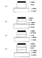
本発明の有機EL素子の基本的な構成を図1(a)〜(d)に示した。 The basic structure of the organic EL device of the present invention is shown in FIGS.
図1に示したように、本発明の有機EL素子は、透明基板15上の透明電極14と金属電極11の間に設けられた単層または複数の有機膜層から構成される。 As shown in FIG. 1, the organic EL element of the present invention is composed of a single layer or a plurality of organic film layers provided between a transparent electrode 14 on a transparent substrate 15 and a metal electrode 11.
図1(a)は、最も単純な構成で、有機層が発光層12のみからなるものである。 FIG. 1A shows the simplest configuration in which the organic layer is composed only of the light emitting layer 12.
図1(b)と(c)は、有機層が2層からなり、それぞれ発光層12とホール輸送層13と、発光層12と電子輸送層16からなる。
In FIG. 1B and FIG. 1C, the organic layer is composed of two layers, which are composed of the light emitting layer 12, the hole transport layer 13, the light emitting layer 12 and the
図1(d)は、有機層が3層からなりホール輸送層13、発光層12および電子輸送層16からなるものである。
In FIG. 1D, the organic layer is composed of three layers, and is composed of the hole transport layer 13, the light emitting layer 12, and the
発光層12には、電子輸送性と発光特性を有するアルミキノリノール錯体など(代表例は、以下に示すAlq)が用いられ、上記金属配位化合物を含有することが好ましい。また、ホール輸送層13には、例えばトリフェニルアミン誘導体(代表例は、以下に示すαNPD)が主に用いられる。また高分子の場合、PVKが用いられる。PVKは、主にホール輸送性であり、PVK自体が青色のEL発光を示す。電子輸送層16としては、例えば、オキサジアゾール誘導体など、または、以下に示すAlq、BphenやBCPを用いることができる。
The light emitting layer 12 is made of an aluminum quinolinol complex having electron transporting properties and light emitting properties (typically, Alq shown below), and preferably contains the metal coordination compound. Further, for the hole transport layer 13, for example, a triphenylamine derivative (a typical example is αNPD shown below) is mainly used. In the case of a polymer, PVK is used. PVK is mainly hole transportable, and PVK itself exhibits blue EL emission. As the
本発明の発光素子を複数備えることで、表示装置を構成することも可能である。 A display device can be configured by providing a plurality of light-emitting elements of the present invention.
<実施例1> <Example 1>
100mlフラスコにNaH(0.196g,4.89mmol,2.1eq)、無水DMF(7ml)を加え、氷浴にて5℃に冷却した。この溶液に無水DMF’(2ml)を溶解させたジエチレングリコール(0.247g,2.33mmol,1.0eq)をゆっくり滴下した。滴下後70℃まで昇温させて30分攪拌後、この溶液を再び20℃に冷却し2−クロロ−1、10−フェナントロリン(1.0g,4.66mmol,2.0eq)を加えて70℃で0.5時間攪拌後さらに140℃に昇温し、3時間攪拌した。この混合液を0℃に冷却し、水(50ml)を投入した後、クロロホルムを加えて有機層を分取した後、水層をさらにクロロホルムで抽出し、有機層を集め、MgSO4で乾燥後、溶媒を留去し、淡黄色の個体を得た。この固体をカラム精製し、再結晶を行うことで無色の結晶であるB1を0.95g得た。 NaH (0.196 g, 4.89 mmol, 2.1 eq) and anhydrous DMF (7 ml) were added to a 100 ml flask and cooled to 5 ° C. in an ice bath. Diethylene glycol (0.247 g, 2.33 mmol, 1.0 eq) in which anhydrous DMF ′ (2 ml) was dissolved was slowly added dropwise to this solution. After the dropwise addition, the temperature was raised to 70 ° C. and stirred for 30 minutes, and then the solution was cooled again to 20 ° C., and 2-chloro-1,10-phenanthroline (1.0 g, 4.66 mmol, 2.0 eq) was added, and 70 ° C. Then, the mixture was further heated to 140 ° C. and stirred for 3 hours. The mixture was cooled to 0 ° C., water (50 ml) was added, chloroform was added to separate the organic layer, the aqueous layer was further extracted with chloroform, the organic layer was collected and dried over MgSO 4. The solvent was distilled off to obtain a pale yellow solid. The solid was purified by column and recrystallized to obtain 0.95 g of B1 as colorless crystals.
50mlフラスコに窒素雰囲気下中、CuI(0.190g,1.00mmol,1eq)、脱水THF30mlを入れ、氷浴下中、B1(0.231g,0.50mmol,1eq)を投入し、室温に戻しながら24時間攪拌を行った。反応後、燈色の沈殿物を濾過によって採取し、脱水エタノール、ヘキサンにて洗浄後、乾燥することによって燈色の粉末である例示化合物A30を350mg(収率83%)得た。 In a 50 ml flask, CuI (0.190 g, 1.00 mmol, 1 eq) and 30 ml of dehydrated THF were placed in a nitrogen atmosphere, and B1 (0.231 g, 0.50 mmol, 1 eq) was charged in an ice bath and returned to room temperature. The mixture was stirred for 24 hours. After the reaction, an amber precipitate was collected by filtration, washed with dehydrated ethanol and hexane, and dried to obtain 350 mg (yield 83%) of Exemplary Compound A30 as an amber powder.
<実施例2> <Example 2>
フェナントロリンを出発物質としてオキシ化、臭素化を片方づつ行うことによってフェナントロリン150g(833mmol)からB2を70g(208mmol)得た。 70 g (208 mmol) of B2 was obtained from 150 g (833 mmol) of phenanthroline by performing oxynation and bromination one by one using phenanthroline as a starting material.
2000mlフラスコにDMF(200ml)とジエチレングリコール(4.5ml,47.5mmol)を加え、0℃に冷却し、アルゴン雰囲気下、攪拌しながら水素化ナトリウム(60%in oil,4.2g,105mmol)を少量ずつ加えた。全量加えた後、室温で30分攪拌し、さらにDMF(1.3L)を加えた。これとは別に10L反応容器にアルゴン雰囲気下でDMF(4.5L)とB2(15g,44.4mmol)を加え、攪拌しながら50℃に加熱を行った。ここに、先ほど作った2000mlフラスコ中の溶液を5時間かけて滴下を行い、その後48時間反応を行った。反応後、溶媒を減圧留去し、水/クロロホルムで抽出を行った。有機層を硫酸マグネシウムで乾燥した後、溶媒を留去し、残渣をクロロホルムで4回再結晶を行うことでB3を3.3g(5.8mmol)得た。 DMF (200 ml) and diethylene glycol (4.5 ml, 47.5 mmol) were added to a 2000 ml flask, cooled to 0 ° C., and sodium hydride (60% in oil, 4.2 g, 105 mmol) was added with stirring under an argon atmosphere. Added in small portions. After the entire amount was added, the mixture was stirred at room temperature for 30 minutes, and DMF (1.3 L) was further added. Separately, DMF (4.5 L) and B2 (15 g, 44.4 mmol) were added to a 10 L reaction vessel under an argon atmosphere, and the mixture was heated to 50 ° C. with stirring. Here, the solution in the 2000 ml flask prepared above was dropped over 5 hours, and then reacted for 48 hours. After the reaction, the solvent was distilled off under reduced pressure and extracted with water / chloroform. The organic layer was dried over magnesium sulfate, the solvent was distilled off, and the residue was recrystallized four times with chloroform to obtain 3.3 g (5.8 mmol) of B3.
100mlフラスコに窒素雰囲気下中、CuI(0.190g,1.00mmol,1eq)、脱水THF40mlを入れ、氷浴下中、B3(0.282g,0.50mmol,1eq)を投入し、室温に戻しながら24時間攪拌を行った。反応後、燈色の沈殿物を濾過によって採取し、脱水エタノール、ヘキサンにて洗浄後、乾燥することによって燈色の粉末である例示化合物A31を290mg(収率61%)得た。 In a 100 ml flask, CuI (0.190 g, 1.00 mmol, 1 eq) and 40 ml of dehydrated THF were placed in a nitrogen atmosphere, and B3 (0.282 g, 0.50 mmol, 1 eq) was charged in an ice bath and returned to room temperature. The mixture was stirred for 24 hours. After the reaction, the amber precipitate was collected by filtration, washed with dehydrated ethanol and hexane, and dried to obtain 290 mg (yield 61%) of Exemplary Compound A31 as an amber powder.
実施例1、2で作製した例示化合物A30,A31の粉末状態での発光特性の測定を行った。結果を表1に示す。また、発光スペクトルを、それぞれ図2,図3に示す。 The emission characteristics of the exemplary compounds A30 and A31 prepared in Examples 1 and 2 in a powder state were measured. The results are shown in Table 1. The emission spectra are shown in FIGS. 2 and 3, respectively.
<実施例3,4>
本実施例では、素子構成として、図1(d)に示す有機層が3層の素子を使用した。
<Examples 3 and 4>
In this example, an element having three organic layers as shown in FIG. 1D was used as the element structure.
ガラス基板(透明基板15)上に100nmのITO(透明電極14)をパターニングして、対向する電極面積が3mm2になるようにした。そのITO基板上に、以下の有機層と電極層を10-4Paの真空チャンバー内で抵抗加熱による真空蒸着し、連続製膜した。有機層2は、金属錯体として例示化合物A30(実施例3)、例示化合物A31(実施例4)を用い、2種類の素子を作製した。
有機層1(ホール輸送層13)(40nm):化合物FL1
有機層2(発光層12)(40,20nm):CBP:金属錯体(A30orA31)(重量比10重量%)
有機層3(電子輸送層16)(50nm):BPhen
金属電極層1(1nm):KF
金属電極層2(100nm):Al
100 nm ITO (transparent electrode 14) was patterned on the glass substrate (transparent substrate 15) so that the opposing electrode area was 3 mm 2 . On the ITO substrate, the following organic layer and electrode layer were vacuum-deposited by resistance heating in a vacuum chamber of 10 −4 Pa to form a continuous film. The organic layer 2 produced two types of devices using the exemplified compound A30 (Example 3) and the exemplified compound A31 (Example 4) as a metal complex.
Organic layer 1 (hole transport layer 13) (40 nm): Compound FL1
Organic layer 2 (light emitting layer 12) (40, 20 nm): CBP: metal complex (A30 or A31) (weight ratio 10% by weight)
Organic layer 3 (electron transport layer 16) (50 nm): BPhen
Metal electrode layer 1 (1 nm): KF
Metal electrode layer 2 (100 nm): Al
<実施例5>
実施例3と同様のITO基板上に、バイエル社製のPEDOT(有機EL用)を40nmの膜厚に1000rpm(20秒)でスピンコートで塗布した。それを120℃の真空チャンバーで1時間乾燥した。
<Example 5>
On the same ITO substrate as in Example 3, PEDOT (for organic EL) manufactured by Bayer was applied to a film thickness of 40 nm by spin coating at 1000 rpm (20 seconds). It was dried in a vacuum chamber at 120 ° C. for 1 hour.
その上に、以下の溶液を用いて、窒素雰囲気下で2000rpm、20秒間でスピンコートすることで、50nmの膜厚の有機膜(発光層12)を形成し、その後、PEDOT製膜時と同じ条件で乾燥した。
脱水クロロベンゼン:10g
ポリビニルカルバゾール(平均分子量9600):92mg
例示化合物A31:8mg
A 50 nm-thick organic film (light-emitting layer 12) is formed thereon by spin coating using the following solution at 2000 rpm for 20 seconds in a nitrogen atmosphere, and then the same as in PEDOT film formation. Dried under conditions.
Dehydrated chlorobenzene: 10g
Polyvinylcarbazole (average molecular weight 9600): 92 mg
Illustrative compound A31: 8 mg
この基板を真空蒸着チャンバーに装着して、Bphenを40nmの膜厚に真空蒸着製膜した。 This substrate was mounted in a vacuum deposition chamber, and Bphen was deposited by vacuum deposition to a film thickness of 40 nm.
有機層の総膜厚は130nmである。 The total thickness of the organic layer is 130 nm.
次に、以下のような構成の陰極(金属電極11)を形成した。
金属電極層1(15nm):AlLi合金(Li含有量1.8重量%)
金属電極層2(100nm):Al
Next, a cathode (metal electrode 11) having the following configuration was formed.
Metal electrode layer 1 (15 nm): AlLi alloy (Li content 1.8 wt%)
Metal electrode layer 2 (100 nm): Al
実施例3〜5で得られた素子に、金属電極11をマイナス、透明電極14をプラスにしてDC電圧を印加して素子特性を評価した。発光スペクトルと発光強度は、スペクトル測定機「SR1」及び「BM7」(トプコン社製)で測定した。電圧印加時の電流値は、「4140B」(ヒューレッドパッカード社製)で測定した。 The device characteristics were evaluated by applying a DC voltage to the devices obtained in Examples 3 to 5 with the metal electrode 11 minus and the transparent electrode 14 plus. The emission spectrum and emission intensity were measured with spectrum measuring instruments “SR1” and “BM7” (manufactured by Topcon). The current value at the time of voltage application was measured by “4140B” (manufactured by Hured Packard).
いずれの素子も電圧電流特性は、良好な整流性を示した。また、電圧を印加した際に発光を確認することが出来た。EL発光は、300、600cd/cm2で発光させた時、2時間たった後も良好な発光を示した。 All of the elements showed good rectification in voltage / current characteristics. Moreover, light emission could be confirmed when a voltage was applied. EL light emission showed good light emission even after 2 hours when light was emitted at 300, 600 cd / cm 2 .
Claims (6)
Priority Applications (1)
| Application Number | Priority Date | Filing Date | Title |
|---|---|---|---|
| JP2004150496A JP4708732B2 (en) | 2004-05-20 | 2004-05-20 | Metal coordination compound for light emitting device and light emitting device using the same |
Applications Claiming Priority (1)
| Application Number | Priority Date | Filing Date | Title |
|---|---|---|---|
| JP2004150496A JP4708732B2 (en) | 2004-05-20 | 2004-05-20 | Metal coordination compound for light emitting device and light emitting device using the same |
Publications (3)
| Publication Number | Publication Date |
|---|---|
| JP2005330233A JP2005330233A (en) | 2005-12-02 |
| JP2005330233A5 JP2005330233A5 (en) | 2010-04-30 |
| JP4708732B2 true JP4708732B2 (en) | 2011-06-22 |
Family
ID=35485136
Family Applications (1)
| Application Number | Title | Priority Date | Filing Date |
|---|---|---|---|
| JP2004150496A Expired - Fee Related JP4708732B2 (en) | 2004-05-20 | 2004-05-20 | Metal coordination compound for light emitting device and light emitting device using the same |
Country Status (1)
| Country | Link |
|---|---|
| JP (1) | JP4708732B2 (en) |
Families Citing this family (3)
| Publication number | Priority date | Publication date | Assignee | Title |
|---|---|---|---|---|
| JP5562657B2 (en) * | 2009-01-23 | 2014-07-30 | 住友化学株式会社 | Organic electroluminescence device |
| CN103254218B (en) * | 2013-04-24 | 2015-09-30 | 宁波大学 | O-phenanthroline m-hydroxybenzoic acid copper ferroelectric function material and preparation method thereof |
| CN115386096B (en) * | 2022-08-11 | 2023-06-02 | 重庆师范大学 | Red fluorescent zinc-based MOF material, preparation method thereof and application thereof in preparing plant growth LED device |
Family Cites Families (1)
| Publication number | Priority date | Publication date | Assignee | Title |
|---|---|---|---|---|
| JP4127755B2 (en) * | 2001-06-20 | 2008-07-30 | 株式会社豊田中央研究所 | Metal complex dye, photoelectrode and dye-sensitized solar cell |
-
2004
- 2004-05-20 JP JP2004150496A patent/JP4708732B2/en not_active Expired - Fee Related
Also Published As
| Publication number | Publication date |
|---|---|
| JP2005330233A (en) | 2005-12-02 |
Similar Documents
| Publication | Publication Date | Title |
|---|---|---|
| JP7226718B2 (en) | Organic light-emitting device, composition and film | |
| TW565604B (en) | Pyrromethene metal complex, material of luminescent element using it and luminescent element | |
| JP5972884B2 (en) | Organic electroluminescence device | |
| KR101005160B1 (en) | Compound for organic electroluminescent device and organic electroluminescent device | |
| JP4870245B2 (en) | Phosphorescent light emitting device material and organic electroluminescent device using the same | |
| JP4545741B2 (en) | Organic electroluminescence device | |
| KR101313730B1 (en) | Organic electroluminescent element | |
| TWI475004B (en) | Organic electroluminescent elements | |
| TWI589562B (en) | Spirobifluorene compounds for light emitting devices | |
| JP5027947B2 (en) | Phosphorescent light emitting device material and organic electroluminescent device using the same | |
| JP5723764B2 (en) | Organic electroluminescence device | |
| US8512877B2 (en) | Naphthyl carbazole derivatives, KL host material, the organic light emitting device employing the same, the display device and the illumination device employing the same | |
| JP2012517422A (en) | Phosphorescent luminescent iridium complexes containing pyridyltriazole ligands | |
| JPWO2005091686A1 (en) | Organic electroluminescence device | |
| JP2014509587A (en) | Novel organometallic compound and organic light emitting device using the same | |
| TW201245150A (en) | Organic electroluminescent element | |
| TW201202195A (en) | Organic electroluminescent element | |
| JPWO2018173598A1 (en) | Organic electroluminescent device | |
| TW200909385A (en) | Host material for blue OLED and white light emitting device utilizing the same | |
| KR20170077806A (en) | Novel heterocyclic compounds and organic light-emitting diode including the same | |
| WO2009107651A1 (en) | Substituted bipyridyl compound and organic electroluminescent element | |
| KR20200096158A (en) | Multicyclic compound and organic light emitting device comprising same | |
| JP4764047B2 (en) | Light emitting element | |
| TWI609872B (en) | Phenanthroline-based compound for organic electroluminescence device | |
| JPWO2003050201A1 (en) | Organic electroluminescence element material |
Legal Events
| Date | Code | Title | Description |
|---|---|---|---|
| A621 | Written request for application examination |
Free format text: JAPANESE INTERMEDIATE CODE: A621 Effective date: 20070507 |
|
| A521 | Request for written amendment filed |
Free format text: JAPANESE INTERMEDIATE CODE: A523 Effective date: 20100312 |
|
| A131 | Notification of reasons for refusal |
Free format text: JAPANESE INTERMEDIATE CODE: A131 Effective date: 20100928 |
|
| A521 | Request for written amendment filed |
Free format text: JAPANESE INTERMEDIATE CODE: A523 Effective date: 20101129 |
|
| A01 | Written decision to grant a patent or to grant a registration (utility model) |
Free format text: JAPANESE INTERMEDIATE CODE: A01 Effective date: 20110315 |
|
| A61 | First payment of annual fees (during grant procedure) |
Free format text: JAPANESE INTERMEDIATE CODE: A61 Effective date: 20110317 |
|
| LAPS | Cancellation because of no payment of annual fees |