JP4708723B2 - Semiconductor memory device - Google Patents
Semiconductor memory device Download PDFInfo
- Publication number
- JP4708723B2 JP4708723B2 JP2004098463A JP2004098463A JP4708723B2 JP 4708723 B2 JP4708723 B2 JP 4708723B2 JP 2004098463 A JP2004098463 A JP 2004098463A JP 2004098463 A JP2004098463 A JP 2004098463A JP 4708723 B2 JP4708723 B2 JP 4708723B2
- Authority
- JP
- Japan
- Prior art keywords
- signal
- address
- latch
- data
- sense
- Prior art date
- Legal status (The legal status is an assumption and is not a legal conclusion. Google has not performed a legal analysis and makes no representation as to the accuracy of the status listed.)
- Expired - Fee Related
Links
Images


Classifications
-
- G—PHYSICS
- G11—INFORMATION STORAGE
- G11C—STATIC STORES
- G11C8/00—Arrangements for selecting an address in a digital store
- G11C8/06—Address interface arrangements, e.g. address buffers
-
- G—PHYSICS
- G11—INFORMATION STORAGE
- G11C—STATIC STORES
- G11C8/00—Arrangements for selecting an address in a digital store
- G11C8/12—Group selection circuits, e.g. for memory block selection, chip selection, array selection
Landscapes
- Engineering & Computer Science (AREA)
- Microelectronics & Electronic Packaging (AREA)
- Dram (AREA)
- Read Only Memory (AREA)
Description
この発明は、ページモード読み出し機能を有する半導体記憶装置に関する。 The present invention relates to a semiconductor memory device having a page mode read function.
メモリセル自体は“H”,“L”レベルの論理出力機能を有さないDRAM等の半導体記憶装置では、メモリセルに記憶されたデータを検知・増幅して論理値(“H”,“L”)に変換させるセンスアンプ動作が必要となる。このセンスアンプ動作を1ワード単位に行っていたのでは著しくデータアクセスが遅くなることから、複数ワード分のメモリセルに記録されたデータを同時に読み出し(センスアンプ動作を含む)て一旦ラッチに蓄えておき、2回目以降のアクセスに対しては上記ラッチからの読み出し時間でアクセス可能になるページモード読み出し機能が広く使用されている。なお、ページモード読み出し機能を備えた半導体記憶装置として、例えば、特許文献1あるいは特許文献2に開示された半導体記憶装置がある。
In a semiconductor memory device such as a DRAM that does not have a logic output function of “H” and “L” levels, the memory cell itself detects and amplifies data stored in the memory cell and outputs a logical value (“H”, “L”). Sense) operation to convert to “)” is required. If this sense amplifier operation is performed in units of one word, data access is remarkably delayed. Therefore, data recorded in memory cells for a plurality of words are simultaneously read (including sense amplifier operation) and temporarily stored in a latch. In addition, for the second and subsequent accesses, a page mode read function that can be accessed in the read time from the latch is widely used. As a semiconductor memory device having a page mode read function, for example, there is a semiconductor memory device disclosed in
半導体記憶装置がページモード読み出し機能を有している場合、例えば、16バイト(128ビット(1バイト=8ビット))のデータを一度に処理可能なLSIからのアクセス要求に対して、半導体記憶装置がデータ出力ピンを16本(16ビット分)有している場合、8ワード(128ビット(1ワード=16ビットで換算))分のページモード機能、すなわち、ページ長が8ワードのページモード機能を有しておれば、1度のセンスアンプ動作によって128ビットのデータ読み出しが実現できるため、当該LSIとの間で高速なデータ送信が可能となる。なお、ページモード読み出し機能を有する半導体記憶装置を用いた電子機器としては例えば携帯電話等が考えられる。 When the semiconductor memory device has a page mode read function, for example, in response to an access request from an LSI that can process 16-byte (128 bits (1 byte = 8 bits)) data at a time, the semiconductor memory device Has 16 data output pins (for 16 bits), page mode function for 8 words (128 bits (1 word = 16 bits converted)), that is, page mode function for page length of 8 words Therefore, since 128-bit data can be read out by one sense amplifier operation, high-speed data transmission can be performed with the LSI. Note that, as an electronic device using a semiconductor memory device having a page mode reading function, for example, a mobile phone is conceivable.
しかしながら、ページモードのワード長を長くすることは、同時に活性化するセンスアンプ数を増加させることなり、かつ、一時的にデータを蓄えるラッチの記憶容量も増加させることになるため、ピーク電流の電流値の増大をもとらし、また、トランジスタや配線のレイアウト面積も増大されるという問題点があった。 However, increasing the page mode word length increases the number of sense amplifiers that are simultaneously activated, and also increases the storage capacity of the latch that temporarily stores data. In addition to the increase in value, the layout area of transistors and wirings is also increased.
この発明は上記問題点を解決するためになされたもので、ピーク電流及びレイアウト面積の増大を最小限に抑えたページモード読み出し機能を有する半導体記憶装置を得ることを目的とする。 The present invention has been made to solve the above-described problems, and an object of the present invention is to obtain a semiconductor memory device having a page mode read function in which an increase in peak current and layout area is minimized.
この発明に係る請求項1記載の半導体記憶装置は、第1及び第2のビット数によって指定される上位及び下位アドレス信号からなるアドレス信号に対応して設けられる複数のメモリセルを有するメモリセルアレイと、前記上位アドレス信号に基づき、前記メモリセルアレイから所定数のメモリセル情報を読み出す読み出し制御部と、前記所定数のメモリセル情報それぞれに対しセンスアンプ動作を行い所定ビット数のセンスデータを得るセンスアンプと、第1のラッチ信号の指示するタイミングで前記所定ビット数のセンスデータをラッチするセンスデータ用ラッチと、第2のラッチ信号の指示するタイミングで前記センスデータ用ラッチに格納された前記所定ビット数のセンスデータをページデータとしてラッチするページデータ用ラッチとを備え、前記ページデータは前記下位アドレス信号に対応してn個の部分ページデータに分類可能であり、前記第1及び第2のラッチ信号を出力するページモード制御回路と、ページモード読み出し期間中において、n回変化する前記下位アドレス信号に基づき、前記n個の部分ページデータを順次ページ選択データとして出力するセレクタ回路とをさらに備え、前記ページ選択データが外部データとして出力され、前記ページモード制御回路は、第1のアドレスを規定する前記上位アドレス信号に基づき前記メモリセルアレイから読み出された前記所定数のメモリセル情報である第1のメモリセル情報群が、前記センスアンプ及び前記センスデータ用ラッチを介して、前記ページデータとして前記ページデータ用ラッチにラッチされた後、前記上位アドレス信号によって規定される前記第1のアドレスの所定ビットを反転させるビット反転処理を行い前記第1のアドレスに続く第2のアドレスを発生させ、前記第1のメモリセル情報群に基づく前記ページモード読み出し期間中に、前記第2のアドレスを規定する前記上位アドレス信号に基づき前記メモリセルアレイから読み出された前記所定数のメモリセル情報である第2のメモリセル情報群を、前記センスアンプを介して前記所定ビット数のセンスデータとして前記センスデータ用ラッチに格納させ、前記第1のメモリセル情報群に関する前記ページモード読み出し期間終了後、前記センスデータ用ラッチに格納された前記第2のメモリセル情報群に基づく前記所定ビット数のセンスデータを、前記ページデータとして前記ページデータ用ラッチにラッチさせることにより、前記第1のメモリセル情報群に基づくページモード読み出し期間後に前記第2のメモリセル情報群に基づく前記ページモード読み出し期間を設定しており、前記ページモード制御回路は、前記上位アドレス信号のアドレス遷移を検出するアドレス遷移検出部を含み、前記アドレス遷移検出部は、前記上位アドレス信号のアドレス遷移を検出して第1のアドレス遷移検出信号を出力する第1のATD回路と、前記上位アドレス信号の前記所定ビットに対応する反転処理アドレス信号のアドレス遷移を検出して第2のアドレス遷移検出信号を出力する第2のATD回路と、前記第1及び第2のアドレス遷移検出信号のうち一方がアドレス遷移を指示するときアドレス遷移を指示する第3のアドレス遷移検出信号を出力するアドレス遷移信号発生手段と含み、前記ページモード制御回路は、前記第3のアドレス遷移検出信号に基づき、前記センスアンプを活性化させるセンス信号及び前記第1のラッチ信号を生成する第1の信号制御回路と、前記第1のアドレス遷移検出信号と前記第1のラッチ信号とを受け、前記第1のアドレス遷移検出信号に基づき前記第2のラッチ信号を生成し、前記第1のアドレス遷移検出信号がアドレス遷移を指示した後における前記第1のラッチ信号による最初のラッチタイミング指示発生時に、前記ビット反転処理の実行を指示する反転指示信号と前記第2のラッチ信号とを生成する第2の信号制御回路とを含む。 According to a first aspect of the present invention, there is provided a semiconductor memory device including a memory cell array having a plurality of memory cells provided corresponding to address signals composed of upper and lower address signals specified by the first and second bit numbers. A read control unit for reading a predetermined number of memory cell information from the memory cell array based on the upper address signal, and a sense amplifier for performing a sense amplifier operation on each of the predetermined number of memory cell information to obtain a predetermined number of bits of sense data A sense data latch for latching the predetermined number of bits of sense data at the timing indicated by the first latch signal, and the predetermined bit stored in the sense data latch at the timing indicated by the second latch signal. Page data latch that latches a number of sense data as page data The page data can be classified into n partial page data corresponding to the lower address signal, and a page mode control circuit for outputting the first and second latch signals, and during a page mode read period And a selector circuit for sequentially outputting the n partial page data as page selection data based on the lower address signal changing n times, and the page selection data is output as external data, and the page mode control The circuit includes a first memory cell information group, which is the predetermined number of memory cell information read from the memory cell array based on the upper address signal defining a first address, for the sense amplifier and the sense data After being latched in the page data latch through the latch as the page data A bit inversion process for inverting a predetermined bit of the first address defined by the upper address signal is performed to generate a second address following the first address, and based on the first memory cell information group During the page mode read period, the second memory cell information group, which is the predetermined number of memory cell information read from the memory cell array based on the upper address signal defining the second address, is used as the sense amplifier. The sense data latch is stored in the sense data latch as the predetermined bit number of sense data via the first and second page mode read periods related to the first memory cell information group, and the second data stored in the sense data latch is stored. The predetermined number of bits of sense data based on the memory cell information group is used as the page data. By latching the Jideta latch, the first of said based on the second memory cell information group after page mode read period based on the memory cell information group has set the page mode readout period, the page mode control circuit Includes an address transition detection unit that detects an address transition of the upper address signal, and the address transition detection unit detects an address transition of the upper address signal and outputs a first address transition detection signal. An ATD circuit; a second ATD circuit that detects an address transition of an inverted address signal corresponding to the predetermined bit of the upper address signal and outputs a second address transition detection signal; and the first and second A third address that instructs address transition when one of the address transition detection signals instructs address transition Address transition signal generating means for outputting a transition detection signal, and the page mode control circuit generates a sense signal for activating the sense amplifier and the first latch signal based on the third address transition detection signal Receiving the first signal control circuit, the first address transition detection signal and the first latch signal, and generating the second latch signal based on the first address transition detection signal, When the first latch timing instruction is generated by the first latch signal after the address transition detection signal of 1 indicates the address transition, an inversion instruction signal for instructing execution of the bit inversion process and the second latch signal are And a second signal control circuit to be generated.
この発明における請求項1記載の半導体記憶装置は、第1のメモリセル情報群に基づく前記ページモード読み出し期間中に、第2のメモリセル情報群を前記センスアンプを介して前記所定ビット数のセンスデータとしてセンスデータ用ラッチに格納させていることにより、第1及び第2のメモリセル情報群によるページモード読み出しを連続的に行える。 According to a first aspect of the present invention, in the semiconductor memory device, the second memory cell information group is sensed with the predetermined number of bits via the sense amplifier during the page mode read period based on the first memory cell information group. By storing the data in the sense data latch as data, the page mode read by the first and second memory cell information groups can be performed continuously.
したがって、連続してページ選択データが読み出せる数であるワード長は、センスアンプ、センスデータ用ラッチ及びページデータ用ラッチに必要な能力に対し2倍となる。 Therefore, the word length, which is the number of page selection data that can be continuously read, is doubled with respect to the capacity required for the sense amplifier, the sense data latch, and the page data latch.
その結果、ページモード読み出し時のピーク電流及びページモード読み出し機能を実現する回路のレイアウト面積の増大を最小限に抑えた半導体記憶装置を得ることができる。 As a result, it is possible to obtain a semiconductor memory device in which the increase in the layout area of the circuit that realizes the peak current and the page mode read function during page mode read is minimized.
<原理>
所定のページ長のページモード読み出し機能を有する半導体記憶装置において、上記ページモード読み出し機能を連続的に複数回動作させることができれば、実質的なページ長を複数倍にするページモード(以下、「シーケンシャルページモード」と呼ぶ)が実現することになり、上述したピーク電流の電流値増大やレイアウト面積増大問題を緩和しつつ高速なデータ転送を確保することが可能となる。しかしながら、本来、外部からのアクセス要求に非同期に動作するページモード読み出し動作時に、内部で自動的にページモード読み出し機能を継続させることは非常に複雑な動作を強いられるため、従来は実現性に乏しかった。特に冗長データとの整合性を実現するのは難しい。このような問題を解消を目指したのが本願発明である。
<Principle>
In a semiconductor memory device having a page mode read function of a predetermined page length, if the page mode read function can be continuously operated a plurality of times, a page mode (hereinafter referred to as “sequential”) that substantially multiplies the page length. (Referred to as “page mode”), and high-speed data transfer can be ensured while alleviating the problems of increase in the peak current value and layout area described above. However, when a page mode read operation that operates asynchronously to an access request from the outside is inherently required to continue the page mode read function automatically inside, it is forced to perform a very complicated operation. It was. In particular, it is difficult to achieve consistency with redundant data. The aimed at solving such a problem is the present invention.
また、本発明は、DRAM等の揮発性半導体記憶装置は勿論、不揮発性半導体記憶装置にも適用可能である。例えば、コントロールゲート,フローティングゲートを有するメモリセルトランジスタで構成されるフラッシュメモリにおけるぺージモード読み出し動作に対しても適用することができる。すなわち、フラッシュメモリのように、複数のビット線のうちYゲートで選択された所定数のビット線に対し、4ワードあるいは8ワード程度の所定数のセンスアンプを設ける構成において、本発明は特に有効である。 Further, the present invention can be applied not only to a volatile semiconductor memory device such as a DRAM but also to a nonvolatile semiconductor memory device. For example, the present invention can also be applied to a page mode read operation in a flash memory composed of memory cell transistors having a control gate and a floating gate. That is, the present invention is particularly effective in a configuration in which a predetermined number of sense amplifiers of about 4 words or 8 words are provided for a predetermined number of bit lines selected by a Y gate among a plurality of bit lines as in a flash memory. It is.
<実施の形態1>
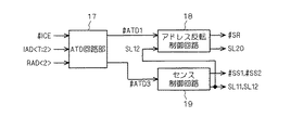
図1はこの発明の実施の形態1である半導体記憶装置のメモリセルアレイ周辺部の構成を示すブロック図である。同図において、内部アドレスIAD<7:5>によってX選択信号SXが選択され、内部アドレスIAD<4:3>及び反転処理アドレスRAD<2>によりY選択信号SYが選択され、64ビットのセンスデータSDが出力され、ページアドレスとして2ビットの内部アドレスIAD<1:0>が用いられる4ワードページの場合が示されている。
<
1 is a block diagram showing a configuration of a memory cell array peripheral portion of a semiconductor memory device according to
メモリセルアレイ1はマトリクス状に配置された複数のメモリセルを有し、X選択信号SXに基づき、複数のメモリセルのうちより選択されたメモリセルからの記憶データを、総計512本のメインビット線MBaそれぞれに読み出す。
The
Yゲート2はY選択信号SYに基づき、512本のメインビット線MBaのうち64本(所定数)を選択してセンスアンプ3に電気的に接続する。
Based on the Y selection signal SY, the
すなわち、内部アドレスIAD<7:3>及び反転処理アドレスRAD<2>からなる上位アドレス信号により、メモリセルアレイ1における64個(所定数)のメモリセル情報がセンスアンプ3に読み出される。なお、反転処理アドレスRAD<2>が上位アドレスにおけるビット反転対象の所定ビットとなる。
That is, 64 (predetermined number) of memory cell information in the
センスアンプ3は、センス信号#SSが“L”のとき活性状態となり、活性状態時にYゲート2より選択された64本のメインビット線MBaに現れる記憶データを検知・増幅するセンスアンプ動作を実行し、64ビット(所定ビット数)構成のセンスデータSDを得る。
The
センスデータ用ラッチ4は、ラッチ信号SL1が“H”のとき活性状態となり、活性状態時にセンスアンプ3により得られた64ビット構成のセンスデータSDとしてラッチする。以降、ラッチ信号SL1が再び“H”になるまでラッチしたセンスデータSDを保持する。したがって、センスアンプ3が非活性状態になっても、センスデータ用ラッチ4にラッチされたセンスデータSDは保持される。
The
ページデータ用ラッチ5は、ラッチ信号SL2が“H”のとき活性状態となり、活性状態時にセンスデータ用ラッチ4に格納されたセンスデータSDをページデータPDとしてラッチする。このページデータPDは下位アドレスである内部アドレスIAD<1:0>に対応して4個の1ワード構成の部分ページデータに分類可能である。
The
セレクタ回路6は、内部アドレスIAD<1:0>で選択されるアドレスに基づき、64ビットのページデータPD(4個の部分ページデータ)から、一の部分ページデータを1ワード(16ビット)のページ選択データPSDとして出力する。すなわち、センスアンプ3,センスデータ用ラッチ4、ページデータ用ラッチ5及びセレクタ回路6による従来レベルのハードウェア構成としては、ページ長が4ワード構成のページモード読み出し機能を有している。
The
出力バッファ7はページ選択データPSDをバッファリングし、外部データDOとして出力する。
The
Xデコーダ8は内部アドレスIAD<7:5>に基づきX選択信号SXを出力し、Yデコーダ9は内部アドレスIAD<4:3>及び反転処理アドレスRAD<2>に基づきY選択信号SYを出力する。したがって、Yゲート2、Xデコーダ8及びYデコーダ9によってメモリセルアレイ1から64ビットのメモリセル情報を読み出す読み出し制御部が構成される。
The
図2は内部アドレスIAD<7:5>、内部アドレスIAD<4:3>及び反転処理アドレスRAD<2>からなる内部アドレスを供給する内部アドレス供給部の構成を示すブロック図である。 FIG. 2 is a block diagram showing a configuration of an internal address supply unit that supplies an internal address composed of an internal address IAD <7: 5>, an internal address IAD <4: 3>, and an inversion processing address RAD <2>.
同図において、CEバッファ11は外部チップイネーブル信号#ECEをバファリングして内部チップイネーブル信号#ICEとして出力する。ADVバッファ12は外部アドレスバリッド(address valid)信号#EADV及び内部チップイネーブル信号#ICEをバファリングして受け内部アドレスバリッド信号#IADVとして出力する。アドレスバッファ13は外部アドレスEAD<7:0>及び内部チップイネーブル信号#ICEをバッファリングし外部アドレスEAD<7:0>をアドレスラッチ回路10に出力する。
In the figure, a
アドレスラッチ回路10は内部アドレスバリッド信号#IADV、外部アドレスEAD<7:0>及び内部チップイネーブル信号#ICEを受け、外部アドレスバリッド信号#EADV及び内部チップイネーブル信号#ICEが“L”のとき、外部アドレスEAD<7:0>及び反転指示信号#SRに基づき、内部アドレスIAD<7:2>、内部アドレスIAD<1:0>及び反転処理アドレスRAD<2>を出力する。
The
図3はアドレスラッチ回路10の内部構成を示す回路図である。同図に示すように、外部アドレスEAD<7:3>をインバータG23が受け、インバータG24の入力がインバータG23の出力及びラッチ64に接続される。そして、インバータG24の出力が内部アドレスIAD<7:3>となる。インバータG23は制御入力に内部アドレスバリッド信号#IADVを受け、内部アドレスバリッド信号#IADVが“L”のときに活性状態となる。
FIG. 3 is a circuit diagram showing an internal configuration of the
なお、実際には外部アドレスEAD<7:3>は5ビットであるため、インバータG23,G24及びラッチ64も外部アドレスEAD<7:3>の各アドレス信号(1ビット分)に対応して総計5つずつ設けられる。本明細書中では、外部アドレスEAD<7:3>等の複数ビットの信号を並列に受ける際に、対応する構成が各ビットにおいて同じ場合、便宜上、1ビット分の構成を代表的に示している場合がある。
Since the external address EAD <7: 3> is actually 5 bits, the inverters G23 and G24 and the
外部アドレスEAD<1:0>をインバータG31が受け、インバータG32の入力がインバータG31の出力及びラッチ67に接続される。そして、インバータG32の出力が内部アドレスIAD<1:0>となる。インバータG31は制御入力に内部アドレスバリッド信号#IADVを受け、内部アドレスバリッド信号#IADVが“L”のときに活性状態となる。
The inverter G31 receives the external address EAD <1: 0>, and the input of the inverter G32 is connected to the output of the inverter G31 and the
反転対象ビットである外部アドレスEAD<2>をインバータG25、G27及びG30の入力が共通に受ける。インバータG26の入力がインバータG25の出力及びラッチ65に接続され、インバータG26の出力がラッチ66及びインバータG29の入力に接続される。インバータG27〜G29は直列に接続され、インバータG29の入力はインバータG26の出力及びラッチ66にも接続される。そして、インバータG29の出力が反転処理アドレスRAD<2>となり、インバータG30の出力が内部アドレスIAD<2>となる。
The inputs of inverters G25, G27, and G30 receive the external address EAD <2> that is the bit to be inverted. The input of the inverter G26 is connected to the output of the inverter G25 and the
このような構成において、アドレスラッチ回路10は、内部アドレスバリッド信号#IADVが“L”のとき、外部アドレスEAD<7:3>及び外部アドレスEAD<1:0>を内部アドレスIAD<7:3>及び内部アドレスIAD<1:0>として出力する。
In such a configuration, when the internal address valid signal #IADV is “L”, the
そして、アドレスラッチ回路10は、アドレス遷移検出信号#ATD1の“L”立ち下がりをトリガとして、外部アドレスEAD<2>を反転処理アドレスRAD<2>として出力し、反転指示信号#SRの“L”立ち下がりをトリガとして外部アドレスEAD<2>の反転信号を反転処理アドレスRAD<2>として出力する。
Then, the
図4は図1で示したメモリセルアレイ1のメモリセルアレイ周辺部に対し各種制御信号を出力するページモード制御回路の主要部の構成を示す回路図である。同図において、ATD回路部14(アドレス遷移検出部)は内部チップイネーブル信号#ICE、内部アドレスIAD<7:2>及び反転処理アドレスRAD<2>を受け、アドレス遷移検出信号#ATD1及び#ATD3を出力する。
FIG. 4 is a circuit diagram showing a configuration of a main part of a page mode control circuit that outputs various control signals to the peripheral portion of the
図5はATD回路部14の内部構成を示す回路図である。同図に示すように、ATD回路31は内部アドレスIAD<7:2>及び内部チップイネーブル信号#ICEを受け、アドレス遷移検出信号#ATD1を出力し、ATD回路32は反転処理アドレスRAD<2>を受け、アドレス遷移検出信号#ATD2を出力する。ANDゲートG1はアドレス遷移検出信号#ATD1及びアドレス遷移検出信号#ATD2を受け、アドレス遷移検出信号#ATD3を出力する。
FIG. 5 is a circuit diagram showing the internal configuration of the
図6はATD回路31の内部構成を示す回路図である。同図に示すように、遷移パルス発生回路33は内部アドレスIAD<7:2>を受け、内部アドレスIAD<7:2>のいずれかのアドレス遷移を検出すると“H”の遷移パルスを発生する。遷移パルス発生回路34は内部チップイネーブル信号#ICEを受け、内部チップイネーブル信号#ICEのエッジ変化を検出すると“H”の遷移パルスを発生する。
FIG. 6 is a circuit diagram showing the internal configuration of the
NMOSトランジスタQ1及びQ2はそれぞれ信号線71と接地レベル間に介挿され、NMOSトランジスタQ1のゲートが遷移パルス発生回路33の出力に接続され、NMOSトランジスタQ2のゲートが遷移パルス発生回路34の出力に接続される。
The NMOS transistors Q1 and Q2 are respectively inserted between the
直列に接続されるインバータG11,G12のインバータG11の入力が信号線71に接続され、PMOSトランジスタQ11は信号線71,電源Vdd間に介挿され、PMOSトランジスタQ11のゲートがインバータG12の出力に接続される。そして、信号線71より得られる信号がアドレス遷移検出信号#ATD1となる。なお、遷移パルス発生回路33及びNMOSトランジスタQ1は内部アドレスIAD<7:2>の各ビットに対応すべく実際にはそれぞれ6個設けられる。
The input of the inverter G11 of the inverters G11 and G12 connected in series is connected to the
図7は遷移パルス発生回路の内部構成を示す回路図である。同図に示す遷移パルス発生回路は、遷移パルス発生回路33,34に相当し、遷移パルス発生回路33の場合、内部アドレスIAD<7:2>の各アドレスビットを入力信号IN1として受け、出力信号OUT1を出力する1ビット分の構成に相当し、遷移パルス発生回路34の場合、内部チップイネーブル信号#ICEを入力信号IN1として受け、出力信号OUT1を出力する構成に相当する。
FIG. 7 is a circuit diagram showing the internal configuration of the transition pulse generating circuit. The transition pulse generating circuit shown in the figure corresponds to the transition
同図に示すように、直列に接続されるインバータG15,G16において、インバータG15の入力に入力信号IN1を受ける。NMOSトランジスタQ4,PMOSトランジスタQ14,抵抗R1,及びキャパシタC1により構成されるL出力遅延インバータ61において、PMOSトランジスタQ14のソースは電源Vddに接続され、ドレイン(ノードN1)は抵抗R1の一端及びキャパシタC1の一方電極に接続される。抵抗R1の他端はNMOSトランジスタQ4のドレインに接続され、NMOSトランジスタQ4のソースは接地され、キャパシタC1の他方電極は接地される。そして、インバータG15の出力がPMOSトランジスタQ14及びNMOSトランジスタQ4のゲートに共通に接続される。
As shown in the figure, in the inverters G15 and G16 connected in series, the input signal IN1 is received at the input of the inverter G15. In the L
NMOSトランジスタQ5,PMOSトランジスタQ15,抵抗R2,及びキャパシタC2により構成されるL出力遅延インバータ62において、PMOSトランジスタQ15のソースは電源Vddに接続され、ドレイン(ノードN2)は抵抗R2の一端及びキャパシタC2の一方電極に接続される。抵抗R2の他端はNMOSトランジスタQ5のドレインに接続され、NMOSトランジスタQ5のソースは接地され、キャパシタC2の他方電極は接地される。そして、インバータG16の出力がPMOSトランジスタQ15及びNMOSトランジスタQ5のゲートに共通に接続される。
In the L
L出力遅延インバータ61は入力(インバータG15の出力)の“H”立ち上がり時は、入力の“L”立ち下がり時に比べて抵抗R1,キャパシタC1の第1のRC時定数で決定される遅延時間分遅れて“L”の反転遅延信号を出力し、L出力遅延インバータ62は入力(インバータG16の出力)の“H”立ち上がり時に、入力が“L”立ち下がり時に比べて抵抗R2,キャパシタC2の第2のRC時定数で決定される遅延時間分遅れて“L”の反転遅延信号を出力する。
The L
NANDゲートG2はノードN1,N2を一方入力,他方入力として受け、その出力がインバータG17の入力に接続され、インバータG17の出力が出力信号OUT1となる。 NAND gate G2 receives nodes N1 and N2 as one input and the other input, its output is connected to the input of inverter G17, and the output of inverter G17 becomes output signal OUT1.
このような構成の遷移パルス発生回路において、通常は、L出力遅延インバータ61,62のうち一方の出力が必ず“L”のため、出力信号OUT1は“L”となっている。
In the transition pulse generating circuit having such a configuration, the output signal OUT1 is normally “L” because one of the L
そして、入力信号IN1の“H”立ち上がり時において、L出力遅延インバータ61の出力の“L”→“H”への変化に対し、L出力遅延インバータ62の出力の“H”→“L”への変化が第2のRC時定数分遅れて生じるため、上記第2のRC時定数分の“H”パルスが出力信号OUT1から発生する。
When the input signal IN1 rises to “H”, the output of the L
同様にして、入力信号IN1の“L”立ち下がり時において、L出力遅延インバータ62の出力の“L”→“H”への変化に対し、L出力遅延インバータ61の出力における“H”→“L”へ変化が第1のRC時定数分遅れて生じるため、上記第1のRC時定数分の“H”パルスが出力信号OUT1から発生する。
Similarly, when the input signal IN1 falls “L”, the output of the L
このように、遷移パルス発生回路は、入力信号IN1の“H”立ち上がり及び“L”立ち下がりの信号遷移時に“H”パルスを発生する出力信号OUT1を出力する。 As described above, the transition pulse generating circuit outputs the output signal OUT1 that generates the “H” pulse at the time of the signal transition of the “H” rising edge and the “L” falling edge of the input signal IN1.
図6に戻って、上記構成のATD回路31は、通常は、PMOSトランジスタQ11により、信号線71は“H”に設定されているため、“H”のアドレス遷移検出信号#ATD1を出力する。そして、内部アドレスIAD<7:2>のアドレス遷移時にNMOSトランジスタQ1が、遷移パルス発生回路33からの“H”の遷移パルス発生時間オンするため、アドレス遷移検出信号#ATD1が所定期間“L”に立ち下がり、同様にして内部チップイネーブル信号#ICEの信号遷移時にNMOSトランジスタQ2が、遷移パルス発生回路34の“H”の遷移パルス発生時間オンするため、アドレス遷移検出信号#ATD1が所定期間“L”に立ち下がる。
Returning to FIG. 6, since the
図8はATD回路32の内部構成を示す回路図である。同図に示すように、遷移パルス発生回路35は反転処理アドレスRAD<2>を受け、反転処理アドレスRAD<2>のアドレス遷移を検出すると“H”の遷移パルスを発生する。
FIG. 8 is a circuit diagram showing the internal configuration of the
NMOSトランジスタQ3は信号線72と接地レベル間に介挿され、NMOSトランジスタQ3のゲートが遷移パルス発生回路35の出力に接続される。
The NMOS transistor Q3 is interposed between the
直列に接続されるインバータG13,G14のインバータG13の入力が信号線72に接続され、PMOSトランジスタQ12は信号線72,電源Vdd間に介挿され、PMOSトランジスタQ12のゲートがインバータG14の出力に接続される。そして、信号線72より得られる信号がアドレス遷移検出信号#ATD2となる。
The input of the inverter G13 of the inverters G13 and G14 connected in series is connected to the
なお、遷移パルス発生回路35は図7で示した構成を呈しており、遷移パルス発生回路35に入力される反転処理アドレスRAD<2>を入力信号IN1として受け、出力信号OUT1を出力する構成に相当する。
The transition
このような構成において、ATD回路32は通常は、PMOSトランジスタQ12により、信号線72は“H”に設定されているため、“H”のアドレス遷移検出信号#ATD2を出力する。そして、反転処理アドレスRAD<2>の遷移時にNMOSトランジスタQ3が、遷移パルス発生回路35からの“H”の遷移パルス発生時間オンするため、アド
In such a configuration, the
図5に戻って、上述したATD回路31,32及びANDゲートG1からなるATD回路部14は、内部アドレスIAD<7:2>あるいは内部チップイネーブル信号#ICEの信号遷移時に“L”パルスを発生するアドレス遷移検出信号#ATD1を出力し、内部アドレスIAD<7:2>、内部チップイネーブル信号#ICEあるいは反転処理アドレスRAD<2>の信号遷移時に“L”パルスを発生するアドレス遷移検出信号#ATD3を出力している。
Returning to FIG. 5, the
図4に戻って、アドレス反転制御回路15(第2の信号制御回路)は、アドレス遷移検出信号#ATD1及びラッチ信号SL1に基づき、反転指示信号#SR及びラッチ信号SL2を出力する。センス制御回路16(第1の信号制御回路)はアドレス遷移検出信号#ATD3に基づきセンス信号#SS及びラッチ信号SL1を出力する。 Returning to FIG. 4, the address inversion control circuit 15 (second signal control circuit) outputs the inversion instruction signal #SR and the latch signal SL2 based on the address transition detection signal # ATD1 and the latch signal SL1. The sense control circuit 16 (first signal control circuit) outputs a sense signal #SS and a latch signal SL1 based on the address transition detection signal # ATD3.
図9はセンス制御回路16の内部構成を示す回路図である。同図に示すように、3段直列に接続される遅延ユニット36〜38のうち初段の遅延ユニット36はアドレス遷移検出信号#ATD3を受け、最終段の遅延ユニット38の出力がセンス信号#SSとなる。3段直列に接続されるインバータG18〜G20のうち初段のインバータG18がセンス信号#SSを受ける。NANDゲートG3は一方入力にセンス信号#SSを他方入力にインバータG20の出力を受ける。NANDゲートG3の出力はインバータG21を介してラッチ信号SL1として出力される。
FIG. 9 is a circuit diagram showing an internal configuration of the
図10は遅延ユニット36(37,38)の内部構成を示す回路図である。同図に示すように、NMOSトランジスタQ6,PMOSトランジスタQ16,抵抗R3,及びキャパシタC3により構成されるL出力遅延インバータ63において、PMOSトランジスタQ16のソースは電源Vddに接続され、ドレイン(ノードN3)は抵抗R3の一端及びキャパシタC3の一方電極に接続される。抵抗R3の他端はNMOSトランジスタQ6のドレインに接続され、NMOSトランジスタQ6のソースは接地され、キャパシタC3の他方電極は接地される。インバータG22の入力がノードN3に接続される。
FIG. 10 is a circuit diagram showing the internal configuration of the delay unit 36 (37, 38). As shown in the figure, in the L
そして、入力信号IN2がPMOSトランジスタQ16及びNMOSトランジスタQ6のゲートに共通に接続され、インバータG22の出力が出力信号OUT2となる。なお、入力信号IN2は遅延ユニット36,37及び38において、アドレス遷移検出信号#ATD3、遅延ユニット36の出力信号、及び遅延ユニット37の出力信号に相当し、出力信号OUT2は遅延ユニット36の出力信号、遅延ユニット37の出力信号、遅延ユニット38の出力信号(センス信号#SS)に相当する。
The input signal IN2 is connected in common to the gates of the PMOS transistor Q16 and the NMOS transistor Q6, and the output of the inverter G22 becomes the output signal OUT2. The input signal IN2 corresponds to the address transition detection signal # ATD3, the output signal of the
このような構成において、遅延ユニット36のL出力遅延インバータ63は入力信号IN2が“H”立ち上がり時に、入力が“L”立ち下がり時に比べて抵抗R3,キャパシタC3の第3のRC時定数で決定される遅延時間分遅れて“L”の反転遅延信号を出力するため、入力信号IN2から出力信号OUT2への“H”立ち上がりの信号伝搬遅延が生じる。一方、入力信号IN2の“L”立ち下がり時は、L出力遅延インバータ63も速やかに“H”の反転信号を出力するため、“L”立ち下がりの信号伝搬遅延が生じない。このように、遅延ユニット36は入力信号IN2の“H”立ち上がり時間を所定時間遅延させて出力信号OUT2を出力する。
レス遷移検出信号#ATD2が所定期間“L”に立ち下がる。
In such a configuration, the L
Less transition detection signal # ATD2 falls to “L” for a predetermined period.
図9に戻って、センス信号#SSは、アドレス遷移検出信号#ATD3の“L”立ち下がりをトリガとして速やかに“L”に立ち下がり、アドレス遷移検出信号#ATD3の“H”立ち上がりをトリガとし、遅延ユニット36〜38による遅延時間後に“H”に立ち上がる信号として出力される。
Referring back to FIG. 9, the sense signal #SS quickly falls to “L” triggered by the “L” falling of the address transition detection signal # ATD3, and triggered by the “H” rising of the address transition detection signal # ATD3. The signal rises to “H” after the delay time by the
一方、ラッチ信号SL1は、通常はNANDゲートG3の一方の入力が“L”のため“L”の信号となり、センス信号#SSの“H”立ち上がり時から所定期間(インバータG18〜G20の信号伝搬遅延時間)のみ“H”パルスを発生する信号となる。 On the other hand, the latch signal SL1 is normally an “L” signal because one input of the NAND gate G3 is “L”, and a predetermined period (signal propagation of the inverters G18 to G20) from the time when the sense signal #SS rises to “H”. Only the (delay time) is a signal for generating an "H" pulse.
図11はアドレス反転制御回路15の内部構成を示す回路図である。同図に示すように、アドレス反転制御回路15はインバータG33、RSフリップフロップ39、1ショットパルス発生回路40、NANDゲートG7及び遅延回路47により構成される。
FIG. 11 is a circuit diagram showing the internal configuration of the address
インバータG33はラッチ信号SL1を受け、その出力がRSフリップフロップ39のS(セット)入力部に入力される。一方、アドレス遷移検出信号#ATD1がRSフリップフロップ39のR(リセット)入力部に入力される。
Inverter G33 receives latch signal SL1, and its output is input to the S (set) input section of RS flip-
RSフリップフロップ39はNANDゲートG4,G5及びインバータG34より構成され、NANDゲートG4,G5の一方入力がそれぞれS入力部、R入力部となり、NANDゲートG4の出力がNANDゲートG5の他方入力として帰還し、NANDゲートG5の出力がNANDゲートG4の他方入力として帰還する。インバータG34は入力がNANDゲートG5の出力に接続され、インバータG34からの出力信号がFF出力信号S39となる。
The RS flip-
このような構成のRSフリップフロップ39において、ラッチ信号SL1の“H”立ち上がりをトリガとしてFF出力信号S39が“H”にセットされ、アドレス遷移検出信号#ATD1の“L”立ち下がりをトリガとして“L”にリセットされる。
In the RS flip-
1ショットパルス発生回路40は直列に接続されたインバータG35〜G37及びNANDゲートG6より構成され、インバータG35の入力がFF出力信号S39を受ける。NANDゲートG6は一方入力にFF出力信号S39を受け、他方入力がインバータG37の出力に接続される。そして、NANDゲートG6の出力信号が遅延回路47を介し反転指示信号#SRとして出力される。なお、アドレス反転制御回路15では遅延回路47を介して反転指示信号#SRを出力する例を示したが、1ショットパルス発生回路40の出力をそのまま反転指示信号#SRとして出力させても良い。
The one-shot
NANDゲートG7は一方入力にNANDゲートG6の出力を受け、他方入力にアドレス遷移検出信号#ATD1を受け、その出力をラッチ信号SL2として出力する。 NAND gate G7 receives the output of NAND gate G6 at one input, receives address transition detection signal # ATD1 at the other input, and outputs the output as latch signal SL2.
このような構成において、1ショットパルス発生回路40から遅延回路47を介して出力される反転指示信号#SRは、通常はNANDゲートG6の一方の入力が“L”のため“H”の信号となり、FF出力信号S39の“H”立ち上がり時から遅延回路47により遅延時間経過後の所定期間(インバータG35〜G37の信号伝搬遅延時間)のみ“L”パルスを発生する信号となる。
In such a configuration, the inversion instruction signal #SR output from the one-shot
したがって、アドレス反転制御回路15は、アドレス遷移検出信号#ATD1の“L”立ち下がりによってRSフリップフロップ39がリセットされた後にラッチ信号SL1の最初の“H”立ち上がりよってRSフリップフロップ39がセットされると、1ショットパルス発生回路40から遅延回路47を介して得られる反転指示信号#SRとして、ビット反転処理を指示する“L”のパルスを発生する。
Therefore, the address
さらに、アドレス反転制御回路15は、1ショットパルス発生回路40の出力信号S40(反転指示信号#SRの遅延前の信号)及びアドレス遷移検出信号#ATD1のうち一方が“L”パルスを発生したとき、ラッチ信号SL2として“L”パルスを発生する。
Further, the address
図12はアドレス反転制御回路15及びその周辺回路の動作を示すタイミング図である。同図に示すように、時刻t1において、内部アドレスIAD<7:2>のアドレス遷移をATD回路部14が検出すると、アドレス遷移検出信号#ATD1が“L”に立ち下がる。
FIG. 12 is a timing chart showing the operation of the address
このアドレス遷移検出信号#ATD1の“L”立ち下がりをトリガとして内部アドレスIAD<2>が反転処理アドレスRAD<2>としてアドレスバッファ13より出力される。同時に、アドレス反転制御回路15のRSフリップフロップ39がリセットされ、FF出力信号S39が“L”となる。
The internal address IAD <2> is output from the
そして、時刻t1から所定時間経過後の時刻t2にラッチ信号SL1の“H”立ち上がりをトリガとしてRSフリップフロップ39がセットされFF出力信号S39が“H”となり、その結果、反転指示信号#SRが“L”に立ち下がる。なお、図12では説明の都合上、1ショットパルス発生回路40の出力信号S40が遅延回路47を介することなくそのまま反転指示信号#SRとして出力される場合を示している。
Then, the RS flip-
この反転指示信号#SRの“L”立ち下がりをトリガとして内部アドレスIAD<2>の反転信号が反転処理アドレスRAD<2>としてアドレスバッファ13より出力される。
The inversion signal of the internal address IAD <2> is output from the
その後、時刻t2から所定時間経過後の時刻t3にラッチ信号SL1が再び“H”に立ち上がる。しかし、FF出力信号S39が時刻t2から“H”であるため、FF出力信号S39が“H”を維持するに留まるため、反転指示信号#SRが“L”に立ち下がることはない。 Thereafter, the latch signal SL1 rises to “H” again at time t3 after a predetermined time has elapsed from time t2. However, since the FF output signal S39 is “H” from the time t2, the FF output signal S39 stays at “H”, so that the inversion instruction signal #SR does not fall to “L”.
その後、時刻t4において、内部アドレスIAD<7:2>のアドレス遷移をATD回路部14が検出すると、アドレス遷移検出信号#ATD1が“L”に立ち下がる。このアドレス遷移検出信号#ATD1の“L”立ち下がりをトリガとして内部アドレスIAD<2>が反転処理アドレスRAD<2>としてアドレスバッファ13より出力される。同時に、アドレス反転制御回路15のRSフリップフロップ39がリセットされ、FF出力信号S39が“L”となる。
Thereafter, when the
図13は図1のセレクタ回路6の内部構成を示す回路図である。同図において、16ビットのページ選択データPSDのうち、所定ビットPSD<k>(k=0〜15のいずれか)に対応し、内部アドレスIAD<1:0>により識別可能なアドレス毎に分類される部分ページデータDI<0>〜DI<3>の選択回路を示している。実際には、図13のような構成がページ選択データPSDの16ビット分存在する。ただし、ページ選択データPSDの各ビットにおいて選択信号SEL<3:0>を生成する回路部分(G101〜G104,G40〜G43)は共有することができる。
FIG. 13 is a circuit diagram showing an internal configuration of the
NANDゲートG101は一方入力に内部アドレスIAD<1>を受け、他方入力に内部アドレスIAD<0>を受け、インバータG40はNANDゲートG101の出力を受ける。 NAND gate G101 receives internal address IAD <1> on one input and internal address IAD <0> on the other input, and inverter G40 receives the output of NAND gate G101.
NANDゲートG102は一方入力に内部アドレスIAD<1>を受け、他方入力に反転内部アドレス#IAD<0>を受け、インバータG41はNANDゲートG102の出力を受ける。なお、反転内部アドレス#IAD<0>は内部アドレスIAD<0>を受けるインバータG39の出力として得ることができる。 NAND gate G102 receives internal address IAD <1> at one input and inverted internal address #IAD <0> at the other input, and inverter G41 receives the output of NAND gate G102. The inverted internal address #IAD <0> can be obtained as an output of the inverter G39 that receives the internal address IAD <0>.
NANDゲートG103は一方入力に反転内部アドレス#IAD<1>を受け、他方入力に内部アドレスIAD<0>を受け、インバータG42はNANDゲートG103の出力を受ける。なお、反転内部アドレス#IAD<1>は内部アドレスIAD<1>を受けるインバータG38の出力として得ることができる。 NAND gate G103 receives inverted internal address #IAD <1> at one input and internal address IAD <0> at the other input, and inverter G42 receives the output of NAND gate G103. The inverted internal address #IAD <1> can be obtained as an output of the inverter G38 that receives the internal address IAD <1>.
NANDゲートG104は一方入力に反転内部アドレス#IAD<1>を受け、他方入力に反転内部アドレス#IAD<0>を受け、インバータG43はNANDゲートG104の出力を受ける。 NAND gate G104 receives inverted internal address #IAD <1> on one input and inverted internal address #IAD <0> on the other input, and inverter G43 receives the output of NAND gate G104.
NANDゲートG105は一方入力に部分ページデータDI<3>を受け、他方入力にインバータG40の出力信号である選択信号SEL<3>を受ける。 NAND gate G105 receives partial page data DI <3> at one input and selection signal SEL <3> which is an output signal of inverter G40 at the other input.
NANDゲートG106は一方入力に部分ページデータDI<2>を受け、他方入力にインバータG41の出力信号である選択信号SEL<2>を受ける。 NAND gate G106 receives partial page data DI <2> at one input and selection signal SEL <2> which is an output signal of inverter G41 at the other input.
NANDゲートG107は一方入力に部分ページデータDI<1>を受け、他方入力にインバータG42の出力信号である選択信号SEL<1>を受ける。 NAND gate G107 receives partial page data DI <1> at one input and selection signal SEL <1> which is an output signal of inverter G42 at the other input.
NANDゲートG108は一方入力に部分ページデータDI<0>を受け、他方入力にインバータG43の出力信号である選択信号SEL<0>を受ける。 NAND gate G108 receives partial page data DI <0> at one input and selection signal SEL <0>, which is an output signal of inverter G43, at the other input.
NANDゲートG109は一方入力及び他方入力にNANDゲートG105及びG106の出力が接続され、NANDゲートG110は一方入力及び他方入力にNANDゲートG107及びNANDゲートG108の出力が接続される。NANDゲートG109及びG110の出力がインバータG44及びG45の入力に接続される。 NAND gate G109 has one input and the other input connected to outputs of NAND gates G105 and G106, and NAND gate G110 has one input and the other input connected to outputs of NAND gate G107 and NAND gate G108. The outputs of NAND gates G109 and G110 are connected to the inputs of inverters G44 and G45.
NANDゲートG111は一方入力及び他方入力がインバータG44及びG45の出力に接続され、NANDゲートG111の出力がページ選択データPSD<k>となる。 One input and the other input of the NAND gate G111 are connected to the outputs of the inverters G44 and G45, and the output of the NAND gate G111 becomes the page selection data PSD <k>.
このような構成において、内部アドレスIAD<1:0>によって選択信号SEL<3:0>のうち一の選択信号のみ“H”となる。ここで、“H”になった選択信号を選択信号SEL<j>(j=0〜3のいずれか)とすると、ページ選択データPSD<k>として部分ページデータDI<j>が出力される。 In such a configuration, only one selection signal among the selection signals SEL <3: 0> is set to “H” by the internal address IAD <1: 0>. Here, if the selection signal that has become “H” is the selection signal SEL <j> (where j = 0 to 3), partial page data DI <j> is output as page selection data PSD <k>. .
図14はこの発明の実施の形態1による半導体記憶装置のページモード読み出し動作を示すタイミング図である。以下、同図を参照して実施の形態1のページモード読み出し動作を説明する。 FIG. 14 is a timing chart showing a page mode read operation of the semiconductor memory device according to the first embodiment of the present invention. Hereinafter, the page mode read operation of the first embodiment will be described with reference to FIG.
まず、時刻t01で内部チップイネーブル信号#ICE及び内部アドレスバリッド信号#IADVが“L”に立ち下がり、アドレスバッファ13が活性状態となり、半導体記憶装置が動作状態となる。
First, at time t01, the internal chip enable signal #ICE and the internal address valid signal #IADV fall to “L”, the
そして、時刻t02で、内部アドレスIAD<7:2>のアドレス遷移がATD回路部14によって検出され、アドレス遷移検出信号#ATD1及び#ATD3が“L”に立ち下がり、同時にセンス信号#SSの“L”立ち下がり、ラッチ信号SL2の“H”立ち上がりが生じる。
At time t02, the address transition of the internal address IAD <7: 2> is detected by the
このときの内部アドレスIAD<2>を“0”とすると、アドレス遷移検出信号#ATD1の“L”立ち下がりをトリガとして、内部アドレスIAD<2>が反転処理アドレスRAD<2>としてアドレスラッチ回路10から出力される。 If the internal address IAD <2> at this time is set to “0”, the address latch circuit uses the falling edge of the address transition detection signal # ATD1 as a trigger to set the internal address IAD <2> as the inversion processing address RAD <2>. 10 is output.
また、上記動作と並行して、Xデコーダ8は内部アドレスIAD<7:5>に基づきX選択信号SXを出力し、Yデコーダ9は内部アドレスIAD<4:3>及び反転処理アドレスRAD<2>に基づきY選択信号SYを出力する。そして、メモリセルアレイ1からX選択信号SXによって選択されたメモリセルの記憶データが512ビットのメインビット線MBaに読み出され、Y選択信号SYに基づきYゲート2により選択された64ビットのデータ(第1のメモリセル情報群)がセンスアンプ3に付与される。
In parallel with the above operation, the
センスアンプ3はセンス信号#SSの“L”立ち下がりにより活性状態となり、センスアンプ動作を行い、時刻t02から時間TS経過後の時刻t03に付与された64ビットのデータのセンス結果(D0xx)が現れる。その後、センス信号#SSが“H”に立ち上がる。
The
その後、時刻t04にラッチ信号SL1が“H”に立ち上がると、これをトリガとしてラッチ信号SL2の“H”立ち上がりが生じる。センスアンプ3のセンス結果がセンスデータSDとしてセンスデータ用ラッチ4にラッチされ、センスデータSDがページデータPD(D0xx)としてページデータ用ラッチ5にラッチされる。
After that, when the latch signal SL1 rises to “H” at time t04, the latch signal SL2 rises to “H” using this as a trigger. The sense result of the
その結果、ページデータ用ラッチ5にラッチされたページデータPDは、セレクタ回路6によって、内部アドレスIAD<1:0>によって最初に指定されるアドレスに対応するページ選択データPSD(D000)が出力バッファ7を介して外部データDOとして出力される。
As a result, the page data PD latched in the page data latch 5 is output by the
このように、センスアンプ3によるセンスアンプ動作が必要なため、最初の外部データDO(D000)が得られるのは、時刻t01〜時刻t04間の時間を要する。
Thus, since the sense amplifier operation by the
その後、ページデータ用ラッチ5にラッチされたページデータPDは、セレクタ回路6により、内部アドレスIAD<1:0>によって指定される順に上述した“D000”以降も、“D001”“D010”“D011”の順に選択された後、出力バッファ7により外部データDOとして連続的に出力するページモード読み出し出力が行われる。すなわち、時刻t04以降、4ワード分のデータが連続して読み出されることになる。
After that, the page data PD latched in the page data latch 5 is “D001”, “D010”, “D011” after “D000” in the order specified by the
一方、時刻t04のラッチ信号SL1の“H”立ち上がりから、遅延回路47による遅延時間経過後の時刻t05に反転指示信号#SRの“L”立ち下がる。この時刻t05において、アドレスラッチ回路10から、内部アドレスIAD<2>の反転信号が反転処理アドレスRAD<2>として出力させることにより、上位アドレスの所定ビットである反転処理アドレスRAD<2>を“0”から“1”擬似的(一時的)に反転するビット反転処理が実行される。なお、ここでいう擬似的に反転するとは、時刻t05〜時刻t08までの一時的な期間において、内部アドレスIAD<2>の“1”を反転させて反転処理アドレスRAD<2>を得ていることを意味する。
On the other hand, the inversion instruction signal #SR falls “L” at time t05 after the delay time by the
その結果、反転処理アドレスRAD<2>のアドレス遷移によって変更されたY選択信号SYに基づき、Yゲート2により選択された新たな64ビットのメモリセル情報(第2のメモリセル情報群)のセンスアンプ3への付与が速やかに行われる。
As a result, sense of new 64-bit memory cell information (second memory cell information group) selected by the
そして、反転処理アドレスRAD<2>のアドレス遷移をトリガとしてアドレス遷移検出信号#ATD3が“L”に立ち下がり、センス信号#SSが“L”に立ち下がり、センスアンプ3が再び活性状態となる。
Then, the address transition detection signal # ATD3 falls to “L”, the sense signal #SS falls to “L”, and the
そして、時刻t05から時間TS経過後の時刻t06に、反転処理アドレスRAD<2>が“1”の場合の(第2のメモリセル情報群に基づく)新たなセンス結果(D1xx)が現れる。その後、センス信号#SSが“H”に立ち上がる。 Then, at time t06 after the elapse of time TS from time t05, a new sense result (D1xx) when the inversion processing address RAD <2> is “1” (based on the second memory cell information group) appears. Thereafter, the sense signal #SS rises to “H”.
時刻t06から所定時間経過後の時刻t07において、ラッチ信号SL1が“H”に立ち上がり、センスデータ用ラッチ4にラッチされるセンスデータSDがD0xx(第1のメモリセル情報群のデータ)からD1xx(第2のメモリセル情報群のデータ)に変更される。 At time t07 after a predetermined time has elapsed from time t06, the latch signal SL1 rises to “H”, and the sense data SD latched in the sense data latch 4 changes from D0xx (data of the first memory cell information group) to D1xx (data of the first memory cell information group). Data of the second memory cell information group).
このように、ラッチ信号SL1はアドレス遷移検出信号#ATD3の“L”立ち下がりに応答して、所定時間経過後“H”となりため、反転処理アドレスRAD<2>のアドレス遷移後のセンスアンプ3より得られるセンス結果を速やかにラッチすることができる。
Thus, since the latch signal SL1 becomes “ H” after a predetermined time has elapsed in response to the “L” falling of the address transition detection signal # ATD3, the
このとき、ラッチ信号SL2は反転処理アドレスRAD<2>のアドレス遷移に関係なく“L”を維持するため、ページデータ用ラッチ5のページデータPDが更新されることなく上述したページモード読み出し出力が支障無く行われる。 At this time, since the latch signal SL2 maintains “L” regardless of the address transition of the inversion processing address RAD <2>, the page mode read output described above is performed without updating the page data PD of the page data latch 5. It is done without hindrance.
このように、ラッチ信号SL1及びSL2のラッチタイミングに連動してビット反転処理を実行する反転指示信号#SRを生成することにより、時刻t04以降において、ページデータ用ラッチ5、セレクタ回路6及び出力バッファ7による前半の4ワード分のデータ(第1のメモリセル情報群に基づくデータ)のページモード読み出し動作に並行して、メモリセルアレイ1、Yゲート2、センスアンプ3、及びセンスデータ用ラッチ4による後半の4ワード分のデータ(第2のメモリセル情報群に基づくデータ)のセンス動作を行うことができる。
As described above, by generating the inversion instruction signal #SR for executing the bit inversion processing in conjunction with the latch timing of the latch signals SL1 and SL2, the page data latch 5 , the
そして、D000〜D003の4ワード分の外部データDOの出力が終える時刻t08に内部アドレスIAD<2>がアドレス変化(“0”→“1”)する。この時刻t08時点において、既にセンスデータ用ラッチ4には次の読み出しデータ(D1xx)がラッチされている。
The internal address IAD <2> changes (“0” → “1”) at time t08 when the output of the external data DO for four words D000 to D003 is completed. At time t08, the next read data (D1xx) is already latched in the
内部アドレスIAD<2>のアドレス遷移検出によるアドレス遷移検出信号#ATD1の“L”立ち下がりに伴い、反転処理アドレスRAD<2>として内部アドレスIAD<2>が出力されるが、時刻t05の際に既に反転処理アドレスRAD<2>は“1”となっているため、結果的に反転処理アドレスRAD<2>は“1”を維持することになる。 The internal address IAD <2> is output as the inversion processing address RAD <2> in response to the falling edge of the address transition detection signal # ATD1 due to the address transition detection of the internal address IAD <2>. Since the inversion processing address RAD <2> is already “1”, the inversion processing address RAD <2> is maintained at “1” as a result.
このとき、ラッチ信号SL2の“H”立ち上がりが生じるため、センスデータSDがページデータ用ラッチ5にラッチされ、ページデータPDが更新されるが、前述したように、時刻t08には外部データDOから“D000”“D001”“D010”“D011”のデータが既に読み出されているため、ページモード読み出し動作に支障は来さない。 At this time, since the latch signal SL2 rises to “H”, the sense data SD is latched in the page data latch 5 and the page data PD is updated. However, as described above, at time t08, from the external data DO. Since the data “D000”, “D001”, “D010”, and “D011” have already been read, the page mode read operation is not hindered.
そして、時刻t08でページデータ用ラッチ5にラッチされたページデータPDは、セレクタ回路6によって、内部アドレスIAD<1:0>によって指定される順に“D100”“D101”“D110”“D111”の順に選択された後、出力バッファ7より外部データDOとして連続的に出力するページモード読み出し出力が行われる。すなわち、時刻t04から8ワードの外部データDO(第1及び第2のメモリセル情報群に基づくデータ)が“D000”“D001”“D010”“D011,“D100”“D101”“D110”“D111”の順で連続的に読み出されることになる。
The page data PD latched in the page data latch 5 at time t08 is “D100”, “D101”, “D110”, and “D111” in the order specified by the internal address IAD <1: 0> by the
なお、時刻t08後の時刻t09にラッチ信号SL1及びラッチ信号SL2の“H”立ち上がりにより、センスアンプ3によるセンス結果でセンスデータ用ラッチ4及びページデータ用ラッチ5の内容が更新されるが、センス結果は時刻t07時点の内容と同様の(D1xx)であるため、実質的にはページデータ用ラッチ5のラッチ内容に変化はないため、動作に支障を来すことはない。
Incidentally, the "H" rise of the latch signal SL1 and the latch signal SL2 at time t09 after the time t08, but the contents of the
このように、アドレスラッチ回路10、ATD回路部14、アドレス反転制御回路15、及びセンス制御回路16等から構成されるページモード制御回路によって以下の動作が行われる。
Thus, the following operations are performed by the page mode control circuit including the
前半4ワードのアドレス(第1のアドレス)を規定する内部アドレスIAD<7:3>及び反転処理アドレスRAD<2>に基づきメモリセルアレイ1から読み出された第1のメモリセル情報群が、センスアンプ3及びセンスデータ用ラッチ4を介して、ページデータPDとしてページデータ用ラッチ5にラッチされた後、反転処理アドレスRAD<2>を擬似的に反転させるビット反転処理を行い前半4ワードのアドレスに続く後半4ワードのアドレス(第2のアドレス)をアドレスラッチ回路10から発生させる。
The first memory cell information group read from the
そして、第1のメモリセル情報群に基づくページモード読み出し期間中に、後半4ワードのアドレスを規定する上位アドレス信号に基づきメモリセルアレイ1から読み出された第2のメモリセル情報群を、センスアンプ3を介して64ビット構成のセンスデータSDとしてセンスデータ用ラッチ4に格納させる。
Then, during the page mode read period based on the first memory cell information group, the second memory cell information group read from the
その後、上記第1のメモリセル情報群に関するページモード読み出し期間終了後、センスデータ用ラッチ4に格納された上記第2のメモリセル情報群に基づく64ビット構成のセンスデータSDを、ページデータPDとしてページデータ用ラッチ5にラッチさせることにより、第1のメモリセル情報群に基づくページモード読み出し期間後に第2のメモリ
Thereafter, the first page mode read period after the completion of a memory cell information group, the sense data SD of 64-bit configuration based on the stored the second memory cell information group in the
その結果、従来レベルのハードウェア構成としては、ページ長が4ワード構成のページモード読み出し機能に抑えながら、実質的にはページ長が8ワード構成のページモード読み出し動作を実現することができる。 As a result, the conventional hardware configuration can realize a page mode read operation having a page length of 8 words, while suppressing the page length to a page mode read function having a page length of 4 words.
したがって、実施の形態1の半導体記憶装置は、同時に活性化するセンスアンプ3のビット数及びラッチ4,5の記憶容量を4ワードページ分に抑えながら、8ワードページ分のページモード読み出し機能を有することになるため、ページモード読み出し時のピーク電流及びページモード読み出し機能を実現する回路のレイアウト面積の増大を最小限に抑えることができる。
Therefore, the semiconductor memory device of the first embodiment has a page mode read function for 8 word pages while suppressing the number of bits of the
本実施の形態では、前半の4ワード分の外部へのページモード読み出し期間中に、後半の4ワード分のデータを読み出している。後半の4ワード分のセンスデータSDが確定すれば直ちに後半の4ワード分の外部へのページモード読み出し期間に移行することも考えられる。 In the present embodiment, data for the last four words is read during the external page mode read period for the first four words. If the sense data SD for the latter four words are determined, it is possible to immediately shift to the page mode read period for the latter four words.
しかしながら、前半の4ワード分の外部へのページモード読み出し動作が確実に行われることを保証するため、前半の4ワード分の外部へのページモード読み出し動作が完了した時刻t08にラッチ信号SL2を“H”にして、後半の4ワード分の外部へのページモード読み出し期間に移行する方が適切である。 However, in order to ensure that the page mode read operation to the outside for the first four words is performed reliably, at time t08 when the page mode read operation to the outside for the first four words is completed, the latch signal SL2 is set to “ It is more appropriate to set it to “H” and shift to the external page mode read period for the latter four words.
なお、本実施の形態では、内部アドレスIAD<1:0>の出力順が“00”,“01”,“10”,“11”の場合を示したが、この順は任意である。 In the present embodiment, the output order of the internal addresses IAD <1: 0> is “00”, “01”, “10”, “11”, but this order is arbitrary.
<実施の形態2>
図15はこの発明の実施の形態2である半導体記憶装置のメモリセルアレイ周辺部の構成を示すブロック図である。同図において、内部アドレスIAD<7:5>によってX選択信号SXが選択され、内部アドレスIAD<4:3>及び反転処理アドレスRAD<2>によりY選択信号SYが選択され、X選択信号SX及びY選択信号SYによって32ビット(所定数)の多値データが読み出され、ページアドレスとして2ビットの内部アドレスIAD<1:0>が用いられる4ワードページの場合が示されている。
<
FIG. 15 is a block diagram showing the configuration of the periphery of the memory cell array of the semiconductor memory device according to the second embodiment of the present invention. In the figure, the X selection signal SX is selected by the internal address IAD <7: 5>, the Y selection signal SY is selected by the internal address IAD <4: 3> and the inversion processing address RAD <2>, and the X selection signal SX In addition, the case of a 4-word page in which 32-bit (predetermined number) multi-value data is read by the Y selection signal SY and the 2-bit internal address IAD <1: 0> is used as the page address is shown.
メモリセルアレイ21はマトリクス状に配置され、各々が4値の多値情報が記憶可能な複数のメモリセルを有し、X選択信号SXに基づき、複数のメモリセルのうちより選択されたメモリセルからの記憶データを、総計256本のメインビット線MBbそれぞれに読み出す。
The
Yゲート22はY選択信号SYに基づき、256本のメインビット線MBbのうち32本(所定数)を選択してセンスアンプ23に電気的に接続する。
The
センスアンプ23は、センス信号#SS2が“L”のとき活性状態となり、活性状態時にYゲート22より選択された、32本のメインビット線MBbに現れる記憶データを検知・増幅するセンスアンプ動作を実行する。センスアンプ動作はセンスアンプ期間中に連続して行う第1及び第2のセンスアンプ動作からなり、センス信号#SS1が“L”のときに行われる第1のセンスアンプ動作により上記記憶データの上位ビット情報が得られ、センス信号#SS1が“H”の時に行われる第2のセンスアンプ動作により上記記憶データの下位ビット情報が得られる。センスアンプ23より得られた32単位のセンス結果(上位ビット情報あるいは下位ビット情報)はセンスデータ用ラッチ24に付与される。
The
センスデータ用ラッチ24は第1センス用ラッチ部24a及び第2センス用ラッチ部24bにより構成される。第1センス用ラッチ部24aは、ラッチ信号SL11が“H”のとき活性状態となり、活性状態時にセンスアンプ23により増幅された32個の上位ビット情報をセンスデータSD1としてラッチする。第2センス用ラッチ部24bは、ラッチ信号SL12が“H”のとき活性状態となり、活性状態時にセンスアンプ23により増幅された32個の下位ビット情報をセンスデータSD2としてラッチする。したがって、センスデータ用ラッチ24は32×2=64ビット(所定ビット数)のセンスデータSD1+SD2をラッチすることになる。
The sense data latch 24 includes a first
以降、第1センス用ラッチ部24a及び第2センス用ラッチ部24bは、それぞれラッチ信号SL11及びSL12が再び“H”になるまでラッチしたセンスデータSD1,SD2を保持する。したがって、センスアンプ23が非活性状態になっても、センスデータ用ラッチ24にラッチされたセンスデータSD1,SD2は保持される。
Thereafter, the first
ページデータ用ラッチ25は、第1センス用ラッチ部25a及び第2センス用ラッチ部25bにより構成され、ラッチ信号SL20が“H”のとき活性状態となり、活性状態時に、センスデータ用ラッチ24に格納されたセンスデータSD1及びSD2を第1及び第2のセンス用ラッチ部25a及び25bにラッチする。そして、第1センス用ラッチ部25aにラッチされたデータが第1ページデータPD1として出力され、第2センス用ラッチ部25bにラッチされたデータが第2ページデータPD2として出力される。第1ページデータPD1及び第2ページデータPD2はそれぞれ4個の部分ページデータに分類可能である。
The page data latch 25 includes a first
セレクタ回路26は第1センス用セレクト部26a及び第2センス用セレクト部26bから構成され、第1センス用セレクト部26a及び第2センス用セレクト部26bは、共通に入力される内部アドレスIAD<1:0>で選択されるアドレスに基づき、ページデータPD1,PD2から8ビットのページ選択データPSD1,PSD2をそれぞれ出力する。すなわち、センスアンプ23,センスデータ用ラッチ24、ページデータ用ラッチ25及びセレクタ回路26による従来レベルのハードウェア構成としては、ページ長が4ワード構成の多値データのページモード読み出し機能を有している。
The
出力バッファ27は第1センス用バッファ部27a及び第2センス用バッファ部27bより構成され、第1及び第2のセンス用バッファ部27a及び27bは、ページ選択データPSD1及びPSD2をバッファリングし、第1及び第2の外部データDO1及びDO2として出力し、第1外部データDO1及び第2外部データDO2からなる外部データDO12が外部データとして最終的に出力される。
The
Xデコーダ28は実施の形態1のXデコーダ8同様、内部アドレスIAD<7:5>に基づきX選択信号SXを出力し、Yデコーダ29は実施の形態1のYデコーダ9同様、内部アドレスIAD<4:3>及び反転処理アドレスRAD<2>に基づきY選択信号SYを出力する。したがって、Yゲート22、Xデコーダ28及びYデコーダ29によってメモリセルアレイ21から32単位の多値メモリセル情報を読み出す読み出し制御部が構成される。
The
なお、内部アドレス供給部の構成は、図2で示した実施の形態1と同様であるため、説明を省略する。 The configuration of the internal address supply unit is the same as that of the first embodiment shown in FIG.
図16は図15で示したメモリセルアレイ21の周辺部に対し各種制御信号を出力するページモード制御回路の主要部の構成を示す回路図である。同図において、ATD回路部17は図4で示した実施の形態1のATD回路部14と同様、内部チップイネーブル信号#ICE、内部アドレスIAD<7:2>及び反転処理アドレスRAD<2>を受け、アドレス遷移検出信号#ATD1及び#ATD3を出力する。
FIG. 16 is a circuit diagram showing a configuration of a main part of a page mode control circuit for outputting various control signals to the peripheral part of the
センス制御回路19はアドレス遷移検出信号#ATD3に基づきセンス信号#SS1及び#SS2並びにラッチ信号SL11及びSL12を出力する。
セル情報群に基づくページモード読み出し期間を連続的に設定する。
The page mode read period based on the cell information group is set continuously.
図17はセンス制御回路19の内部構成を示す回路図である。同図に示すように、3段直列に接続される遅延ユニット41〜43のうち初段の遅延ユニット41はアドレス遷移検出信号#ATD3を受け、最終段の遅延ユニット43の出力がセンス信号#SS1となる。3段直列に接続されるインバータG46〜G48のうち初段のインバータG46がセンス信号#SS1を受ける。NANDゲートG112は一方入力にセンス信号#SS1を他方入力にインバータG48の出力を受ける。NANDゲートG112の出力はインバータG49を介してラッチ信号SL11として出力される。
FIG. 17 is a circuit diagram showing the internal configuration of the
さらに、3段直列に接続される遅延ユニット44〜46のうち初段の遅延ユニット44はセンス信号#SS1を受け、最終段の遅延ユニット46の出力がセンス信号#SS2となる。3段直列に接続されるインバータG50〜G52のうち初段のインバータG50がセンス信号#SS2を受ける。NANDゲートG113は一方入力にセンス信号#SS2を他方入力にインバータG52の出力を受ける。NANDゲートG113の出力はインバータG53を介してラッチ信号SL12として出力される。なお、遅延ユニット41〜46の内部構成は、図10で示した実施の形態1の遅延ユニット36〜38の内部構成と同様である。
Further, among the
このような構成において、センス信号#SS1及び#SS2は、アドレス遷移検出信号#ATD3の“L”立ち下がりをトリガとして共に速やかに“L”に立ち下がり、アドレス遷移検出信号#ATD3の“H”立ち上がりをトリガとし、遅延ユニット41〜43及び遅延ユニット41〜46による遅延時間後にそれぞれ“H”に立ち上がる信号として出力される。
In such a configuration, the sense signals # SS1 and # SS2 quickly fall to “L” with the “L” falling edge of the address transition detection signal # ATD3 as a trigger, and “H” of the address transition detection signal # ATD3. The signal is output as a signal that rises to “H” after the delay time by the
一方、ラッチ信号SL11及びSL12は、通常はNANDゲートG112及びG113の一方の入力が“L”のため“L”の信号となり、センス信号#SS1及び#SS2の“H”立ち上がり時から所定期間(インバータG46〜G48及びインバータG50〜52の信号伝搬遅延時間)のみそれぞれ“H”パルスを発生する信号となる。 On the other hand, the latch signals SL11 and SL12 are normally “L” signals because one input of the NAND gates G112 and G113 is “L”, and the latch signals SL11 and SL12 have a predetermined period (from the time when the sense signals # SS1 and # SS2 rise to “H”. Only the signal propagation delay times of the inverters G46 to G48 and the inverters G50 to 52 are signals that generate “H” pulses.
図16に戻って、アドレス反転制御回路18は、アドレス遷移検出信号#ATD1及びラッチ信号SL12に基づき、反転指示信号#SR及びラッチ信号SL20を出力する。内部構成は、入力信号となるラッチ信号SL1がラッチ信号SL12に置き換わり、出力信号となるラッチ信号SL2がラッチ信号SL20に置き換わった点を除き、図11で示して実施の形態1のアドレス反転制御回路15と同様である。
Returning to FIG. 16, the address
上述したアドレスラッチ回路10(実施の形態1と同じ)、ATD回路部17、アドレス反転制御回路18及びセンス制御回路19等により、実施の形態1と同様なページモード制御が可能なページモード制御回路を構成する。
Page mode control circuit capable of performing the same page mode control as in the first embodiment by the address latch circuit 10 (same as in the first embodiment), the
図18はこの発明の実施の形態2による半導体記憶装置のページモード読み出し動作を示すタイミング図である。以下、同図を参照して実施の形態2のページモード読み出し動作を説明する。 FIG. 18 is a timing chart showing a page mode read operation of the semiconductor memory device according to the second embodiment of the present invention. Hereinafter, the page mode read operation of the second embodiment will be described with reference to FIG.
まず、時刻t11で内部チップイネーブル信号#ICE及び内部アドレスバリッド信号#IADVが“L”に立ち下がり、アドレスバッファ13が活性状態となり、半導体記憶装置が動作状態となる。
First, at time t11, the internal chip enable signal #ICE and the internal address valid signal #IADV fall to “L”, the
そして、時刻t12で、内部アドレスIAD<7:2>のアドレス遷移がATD回路部17によって検出され、アドレス遷移検出信号#ATD1及び#ATD3が“L”に立ち下がり、同時にセンス信号#SS2(#SS1)の“L”立ち下がり、ラッチ信号SL20の“H”立ち上がりが生じる。
At time t12, the address transition of the internal address IAD <7: 2> is detected by the
このときの内部アドレスIAD<2>を“0”とすると、アドレス遷移検出信号#ATD1の“L”立ち下がりをトリガとして、内部アドレスIAD<2>が反転処理アドレスRAD<2>としてアドレスラッチ回路10から出力される。 If the internal address IAD <2> at this time is set to “0”, the address latch circuit uses the falling edge of the address transition detection signal # ATD1 as a trigger to set the internal address IAD <2> as the inversion processing address RAD <2>. 10 is output.
また、上記動作と並行して、Xデコーダ28は内部アドレスIAD<7:5>に基づきX選択信号SXを出力し、Yデコーダ29は内部アドレスIAD<4:3>及び反転処理アドレスRAD<2>に基づきY選択信号SYを出力する。そして、メモリセルアレイ21からX選択信号SXによって選択されたメモリセルの記憶データが256ビットのメインビット線MBbに読み出され、Y選択信号SYに基づきYゲート22により選択された32単位の多値データがセンスアンプ23に付与される。
In parallel with the above operation, the
センスアンプ23はセンス信号#SS2の“L”立ち下がりにより活性状態となり、第1のセンスアンプ動作を行い、時刻t12から時間TS1経過後の時刻t13に、Yゲート22より付与された32単位のデータの上位ビット情報のセンス結果(D0xxF)が現れ、このとき、ラッチ信号SL11の“H”立ち上がりによりセンス結果が第1センスデータSD1としてラッチされる。
The
時刻t13とほぼ同時にセンス信号#SS1が“H”に立ち上がり、センスアンプ23は第2のセンスアンプ動作を開始し、時刻t13から時間TS2経過後の時刻t14に、Yゲート22より付与された32単位のデータの下位ビット情報のセンス結果(D0xxS)が現れ、このとき、第1ラッチ信号SL12の“H”立ち上がりによりセンス結果が第2センスデータSD2としてラッチされる。
At substantially the same time as time t13, the sense signal # SS1 rises to “H”, the
時刻t14にラッチ信号SL12が“H”に立ち上がると、これをトリガとして反転指示信号#SRの“L”立ち下がり及びラッチ信号SL20の“H”立ち上がりが生じる。その結果、ページデータ用ラッチ25における第1及び第2センス用ラッチ部25a及び25bの第1及び第2のページデータPD1及びPD2として、第1及び第2のセンスデータSD1及びSD2がラッチされる。
When the latch signal SL12 rises to “H” at time t14, this triggers the “L” falling of the inversion instruction signal #SR and the “H” rising of the latch signal SL20. As a result, the first and second sense data SD1 and SD2 are latched as the first and second page data PD1 and PD2 of the first and second
そして、ページデータ用ラッチ25にラッチされたページデータPD1及びPD2は、セレクタ回路26によって、内部アドレスIAD<1:0>によって最初に指定されるアドレスに対応するページ選択データPSD(D000(D000F,D000S))が出力バッファ27を介して外部データDO12として出力される。
Then, the page data PD1 and PD2 latched in the page data latch 25 are converted by the
このように、センスアンプ23によるセンスアンプ動作が必要なため、最初の外部データDO12(D000)が得られるのは、時刻t11〜時刻t14間の時間を要する。
Thus, since the sense amplifier operation by the
その後、ページデータ用ラッチ25にラッチされたページデータPDは、セレクタ回路26により、内部アドレスIAD<1:0>によって指定される順に上述した“D000”以降も、“D001(D001F,D001S)”“D010(D010F,D010S)”“D011(D011F,D011S)”の順に選択された後、出力バッファ27により外部データDO12として連続的に出力するページモード読み出し出力が行われる。すなわち、時刻t14以降、4ワード分のデータが連続して読み出されることになる。
After that, the page data PD latched in the page data latch 25 is "D001 (D001F, D001S)" after the above-mentioned "D000" in the order specified by the internal address IAD <1: 0> by the
一方、時刻t14から少し遅れた時刻t15において反転指示信号#SRの“L”立ち下がりにより、内部アドレスIAD<2>の反転信号が反転処理アドレスRAD<2>として出力されることにより、反転処理アドレスRAD<2>が“0”から“1”に反転される。 On the other hand, the inversion signal of the internal address IAD <2> is output as the inversion processing address RAD <2> due to the “L” falling of the inversion instruction signal #SR at the time t15 slightly delayed from the time t14. The address RAD <2> is inverted from “0” to “1”.
その結果、反転処理アドレスRAD<2>のアドレス遷移によって変更されたY選択信号SYに基づき、Yゲート22により選択された新たな32単位の多値データがセンスアンプ23に付与される。
As a result, based on the Y selection signal SY changed by the address transition of the inversion address RAD <2>, new 32-unit multi-value data selected by the
そして、反転処理アドレスRAD<2>のアドレス遷移をトリガとしてアドレス遷移検出信号#ATD3が“L”に立ち下がり、第2のセンス信号#SS2が“L”に立ち下がり、センスアンプ23が再び活性状態となり、第1のセンスアンプ動作を開始する。
Then, the address transition detection signal # ATD3 falls to “L”, the second sense signal # SS2 falls to “L”, and the
そして、時刻t15から時間TS1経過後の時刻t16に、反転処理アドレスRAD<2>が“1”の場合の新たなセンス結果(D1xxF)が現れる。このとき、ラッチ信号SL11の“H”立ち上がりによりセンス結果が第1センスデータSD1としてラッチされる。すなわち、第1センス用ラッチ部24aにラッチされる第1センスデータSD1がD0xxFからD1xxFに変更される。
Then, a new sense result (D1xxF) appears when the inversion processing address RAD <2> is “1” at time t16 after time TS1 has elapsed from time t15. In this case, "H" sensing result by the rise of latches signal SL11 is latched as the first sense data SD1. That is, the first sense data SD1 latched in the first
時刻t16とほぼ同時に、センス信号#SS1が“H”に立ち上がり、センスアンプ23は第2のセンスアンプ動作を開始する。センス信号#SS1の“H”立ち上がり後、時間TS2経過後の時刻t17に、Yゲート22より付与された32単位のデータの下位ビット情報のセンス結果(D1xxS)が現れ、このとき、ラッチ信号SL12の“H”立ち上がりによりセンス結果が第2センスデータSD2としてラッチされる。すなわち、第2センス用ラッチ部24bにラッチされる第2センスデータSD2がD0xxSからD1xxSに変更される。
At substantially the same time as the time t16, the rise in the sense signal # SS1 is "H", the
このとき、ラッチ信号SL20は“L”を維持するため、ページデータ用ラッチ25のページデータPD1及びPD2が更新されることなく上述したページモード読み出し出力が支障無く行われる。 At this time, since the latch signal SL20 is maintained at “L”, the page data read output described above is performed without any trouble without updating the page data PD1 and PD2 of the page data latch 25.
このように、時刻t14以降において、ページデータ用ラッチ25、セレクタ回路26及び出力バッファ27による前半の4ワード分のデータの外部データDO12としての出力動作に並行して、メモリセルアレイ21、Yゲート22、センスアンプ23、及びセンスデータ用ラッチ24による後半の4ワード分のデータのセンス動作が行われる。
Thus, after time t14, in parallel with the output operation of the data for the first four words by the page data latch 25 ,
そして、D000〜D003の4ワード分の外部データDO12の出力が終える時刻t18に内部アドレスIAD<2>がアドレス変化(“0”→“1”)する。この時刻t18時点において、既にセンスデータ用ラッチ24には次の読み出しデータ(D1xx(D1xxF,D1xxS))がラッチされている。 Then, the internal address IAD <2> is an address change to 4-word time t18 the output of the external data DO 12 finishes of D000~D003 ( "0" → "1 ") to. At time t18, the next read data (D1xx (D1xxF, D1xxS)) has already been latched in the sense data latch 24.
内部アドレスIAD<2>のアドレス遷移検出によるアドレス遷移検出信号#ATD1の“L”立ち下がりに伴い、反転処理アドレスRAD<2>として内部アドレスIAD<2>が出力されるが、時刻t15の際に既に反転処理アドレスRAD<2>は“1”となっているため、結果的に反転処理アドレスRAD<2>は“1”を維持することになる。 The internal address IAD <2> is output as the inversion processing address RAD <2> in response to the falling edge of the address transition detection signal # ATD1 due to the address transition detection of the internal address IAD <2>. Since the inversion processing address RAD <2> is already “1”, the inversion processing address RAD <2> is maintained at “1” as a result.
このとき、ラッチ信号SL20の“H”立ち上がりが生じるため、センスデータSD1,SD2がページデータ用ラッチ25にラッチされ、ページデータPD1,PD2が更新されるが、前述したように、時刻t18には外部データDO12から“D000”“D001”“D010”“D011”のデータが既に読み出されているため、ページモード読み出し動作に支障は来さない。 At this time, since the latch signal SL20 rises to “H”, the sense data SD1 and SD2 are latched in the page data latch 25 and the page data PD1 and PD2 are updated. However, as described above, at time t18. Since the data “D000”, “D001”, “D010”, and “D011” have already been read from the external data DO 12 , there is no problem in the page mode read operation.
そして、時刻t18でページデータ用ラッチ25にラッチされたページデータPD1,PD2は、セレクタ回路26によって、内部アドレスIAD<1:0>によって指定される順に“D100(D100F,D100S)”,“D101(D101F,D101S)”,“D110(D110F,D110S)”,“D111(D111F,D111S)”の順に選択された後出力バッファ27により外部データDO12として連続的に出力するページモード読み出し出力が行われる。すなわち、時刻t14から8ワードの外部データDO12が“D000”“D001”“D010”“D011,“D100”“D101”“D110”“D111”の順で連続的に読み出されることになる。
The page data PD1 and PD2 latched in the page data latch 25 at time t18 are "D100 (D100F, D100S)", "D101" by the
なお、時刻t18後の時刻t19における第1ラッチ信号SL11の“H”立ち上がりにより第1センス用ラッチ部24aの内容が更新され、時刻t20におけるラッチ信号SL12及びラッチ信号SL20の“H”立ち上がりにより、第2センス用ラッチ部24b及びページデータ用ラッチ25の内容が更新されるが、センス結果は時刻t17時点の内容と同様の(D1xx(D1xxF,D1xxS))であるため、実質的にはページデータ用ラッチ25のラッチ内容に変化はないため、動作に支障を来すことはない。
The contents of the first
このように、実施の形態2の半導体記憶装置は、ラッチ信号SL12及びラッチ信号SL20の“H”立ち上りによってページデータ用ラッチ25へのラッチ完了時を基準として、反転指示信号#SRを“L”の活性状態とすることにより、前半のページデータのページモード読み出し機能に支障無く、かつ後半のページデータのセンス動作を実行している。 Thus, the semiconductor memory device of the second embodiment, with reference to the time latch completion of the page data latch 25 by "H" rise of latches signal SL12 and latch signals SL20, the inversion command signal #SR " By setting the L ″ active state, the page mode read function of the first half page data is not affected, and the second page data sense operation is executed.
その結果、実施の形態2の半導体記憶装置は、実施の形態1と同様、同時に活性化するセンスアンプ23のビット数及びラッチ24,25の記憶容量を4ワードページ分に抑えながら、8ワードページ分のページモード読み出し機能を有することになるため、ページモード読み出し時のピーク電流及びページモード読み出し機能を実現する回路のレイアウト面積の増大を最小限に抑えることができる。
As a result, in the semiconductor memory device of the second embodiment, as in the first embodiment, the number of bits of the
なお、実施の形態2では、実施の形態1同様、内部アドレスIAD<1:0>の出力順が“00”,“01”,“10”,“11”の場合を示したが、この順は任意である。 In the second embodiment, as in the first embodiment, the output order of the internal addresses IAD <1: 0> is “00”, “01”, “10”, “11”. Is optional.
加えて、実施の形態2の半導体記憶装置は、3ビット以上の多値情報を記憶するメモリセルから構成されるメモリセルアレイ21に対し、上記した効率的なページモード読み出し機能を有するという効果を奏している。
In addition, the semiconductor memory device according to the second embodiment has an effect of having the above-described efficient page mode read function for the
なお、実施の形態2では多値情報として4値記憶の場合を示したが、3値、5値以上の多値記憶に応用することができる。例えば、8値の場合は各構成部の個数mを現在の“2”から“3”((23)=8)に拡張することにより実現することができる。 In the second embodiment, the case of quaternary storage is shown as multi-value information, but it can be applied to multi-value storage of ternary values, quinary values or more. For example, eight values can be realized by expanding the number m of each component from the current “2” to “3” ((2 3 ) = 8).
<実施の形態3>
図19はこの発明の実施の形態3である半導体記憶装置のメモリセルアレイ周辺部の構成を示すブロック図である。同図において、構成要素1〜9は実施の形態1で示した構成と同様であり、同一符号を付している。
<
FIG. 19 is a block diagram showing the structure of the periphery of the memory cell array of the semiconductor memory device according to the third embodiment of the present invention. In the figure,
スペアメモリセルアレイ51は複数のスペアメモリセルを有し、X選択信号SXに基づき、複数のスペアメモリセルのうちより選択されたスペアメモリセルからの記憶データ(スペア情報)を、総計8本のメインビット線MBsそれぞれに読み出す。
The spare
Yゲート52はスペアY選択信号SSYに基づき、8本のメインビット線MBsのうち1本(所定のスペア数)を選択してセンスアンプ3に電気的に接続する。
The Y gate 52 selects one (predetermined number of spares) of the eight main bit lines MBs based on the spare Y selection signal SSY and electrically connects it to the
センスアンプ53(置換用センスアンプ)は、センス信号#SSが“L”のとき活性状態となり、活性状態時にYゲート52より選択された1本のメインビット線MBsに現れる記憶データを検知・増幅するセンスアンプ動作を実行する。 The sense amplifier 53 (replacement sense amplifier) is activated when the sense signal #SS is “L”, and detects and amplifies storage data appearing on one main bit line MBs selected by the Y gate 52 when activated. Execute the sense amplifier operation.
センスデータ用ラッチ54(スペアセンス用ラッチ)は、ラッチ信号SL1が“H”のとき活性状態となり、活性状態時にセンスアンプ53により増幅された1本(所定スペアビット数)のメインビット線MBs上の信号をスペアセンスデータSSD1としてラッチする。以降、ラッチ信号SL1が再び“H”になるまでラッチしたスペアセンスデータSSD1を保持する。したがって、センスアンプ53が非活性状態になっても、センスデータ用ラッチ54にラッチされたスペアセンスデータSSD1は保持される。
The sense data latch 54 (spare sense latch) is activated when the latch signal SL1 is “H”, and on one main bit line MBs (a predetermined number of spare bits ) amplified by the
ページデータ用ラッチ55(スペアデータ用ラッチ)は、ラッチ信号SL2が“H”のとき活性状態となり、活性状態時にセンスデータ用ラッチ54に格納されたスペアセンスデータSSD1をスペアデータSSD2としてラッチする。 The page data latch 55 (spare data latch) is activated when the latch signal SL2 is “H”, and latches the spare sense data SSD1 stored in the sense data latch 54 as spare data SSD2 when activated.
図20はスペアY選択信号SSYを発生するスペア制御回路20の構成を示すブロック図である。同図に示すように、スペア制御回路20は内部アドレスIAD<4:3>及び反転処理アドレスRAD<2>に基づきスペアY選択信号SSYを決定し出力する。また、スペアY選択信号SSYより選択されたデータにおける置換情報を示す冗長置換情報RDを出力する。
FIG. 20 is a block diagram showing a configuration of
したがって、Xデコーダ8(実施の形態1と同じ)、スペア制御回路20及びYゲート52によりスペアメモリセルアレイ51からスペア情報を読み出すスペア読み出し制御部を構成することになる。
Accordingly, the X decoder 8 (same as in the first embodiment), the
スワップ回路56(置換実行回路)はページ選択データPSDを受け、冗長置換情報RD及び冗長情報シフト信号RSF(置換情報取り込み制御信号)に規定された指示に従い、置換が必要な場合、ページ選択データPSDのうちの所定ビットデータを置換用1ビットデータであるスペアデータSSD2に置換して、置換済みページ選択データS56を出力する。 The swap circuit 56 (replacement execution circuit) receives the page selection data PSD, and if the replacement is required according to the instructions defined in the redundant replacement information RD and the redundant information shift signal RSF (replacement information capture control signal), the page selection data PSD The predetermined page data is replaced with spare data SSD2 which is 1-bit data for replacement, and replaced page selection data S56 is output.
出力バッファ7は置換済みページ選択データS56をバッファリングして外部データDOとして出力する。
The
図21はスワップ回路56の内部構成を示す回路図である。同図に示すように、インバータG54(実際は16個あり、代表的に1つを示す)は、ページ選択データPSDを入力し、インバータG55(実際は16個あり、代表的に1つを示す)はスペアデータSSD2を受ける。すなわち、16個のインバータG55は全て同じスペアデータSSD2を受ける。
FIG. 21 is a circuit diagram showing the internal configuration of the
一方、ラッチ68はNMOSトランジスタQ7(実際は6個あり、代表的に1つを示す)を介して冗長置換情報RDを受ける。冗長置換情報RDには2ビットのアドレス置換情報RA<1:0>と4ビットの冗長置換情報RD<3:0>からなる6ビット情報であり、NMOSトランジスタQ7がオン状態時にラッチ68に取り込まれる。
On the other hand, the
NMOSトランジスタQ7はゲートに冗長情報シフト信号RSFを受ける。したがって、冗長情報シフト信号RSFが“H”のとき冗長置換情報RDがラッチ68に取り込まれる。判定回路69はラッチ68の出力と内部アドレスIAD<1:0>とを受け、置換信号HIT<15:0>を出力する。
NMOS transistor Q7 receives redundant information shift signal RSF at its gate. Therefore, redundant replacement information RD is taken into
置換信号HIT<15:0>は、16個のインバータG54及びG55の反転制御入力及び制御入力に付与される。置換信号HIT<15:0>は通常、全て“0”であり、置換が必要な際は所定ビットのみ“1”となる。 The replacement signal HIT <15: 0> is applied to the inversion control input and control input of the 16 inverters G54 and G55. The replacement signals HIT <15: 0> are normally all “0”, and only a predetermined bit is “1” when replacement is necessary.
したがって、通常はページ選択データPSDがそのまま置換済みページ選択データS56をして出力され、置換時はページ選択データPSDのうち置換信号HIT<15:0>の指示する所定ビットがスペアデータSSD2に置換されて得られるデータが置換済みページ選択データS56として出力される。 Therefore, normally, page selection data PSD is output as replacement page selection data S56 as it is, and at the time of replacement, a predetermined bit indicated by replacement signal HIT <15: 0> in page selection data PSD is replaced with spare data SSD2. The obtained data is output as replaced page selection data S56.
図22は判定回路69の内部構成を示す回路図である。同図に示すように、冗長置換情報RD<3:0>はインバータG56〜G59によりそれぞれ反転され、反転冗長置換情報#RD<3:0>が得られている。
FIG. 22 is a circuit diagram showing the internal configuration of the
NANDゲートG114は一方入力及び他方入力に反転冗長置換情報#RD<0>及び反転冗長置換情報#RD<1>を受ける。NANDゲートG115は一方入力及び他方入力に冗長置換情報RD<0>及び反転冗長置換情報#RD<1>を受ける。NANDゲートG116は一方入力及び他方入力に反転冗長置換情報#RD<0>及び冗長置換情報RD<1>を受ける。NANDゲートG117は一方入力及び他方入力に冗長置換情報RD<0>及び冗長置換情報RD<1>を受ける。 NAND gate G114 receives inverted redundant replacement information #RD <0> and inverted redundant replacement information #RD <1> at one input and the other input. NAND gate G115 receives redundant replacement information RD <0> and inverted redundant replacement information #RD <1> at one input and the other input. NAND gate G116 receives inverted redundant replacement information #RD <0> and redundant replacement information RD <1> at one input and the other input. NAND gate G117 receives redundant replacement information RD <0> and redundant replacement information RD <1> at one input and the other input.
NANDゲートG118は一方入力及び他方入力に反転冗長置換情報#RD<2>及び反転冗長置換情報#RD<3>を受ける。NANDゲートG119は一方入力及び他方入力に冗長置換情報RD<2>及び反転冗長置換情報#RD<3>を受ける。NANDゲートG120は一方入力及び他方入力に反転冗長置換情報#RD<2>及び冗長置換情報RD<3>を受ける。NANDゲートG121は一方入力及び他方入力に冗長置換情報RD<2>及び冗長置換情報RD<3>を受ける。 NAND gate G118 receives inverted redundant replacement information #RD <2> and inverted redundant replacement information #RD <3> at one input and the other input. NAND gate G119 receives redundant replacement information RD <2> and inverted redundant replacement information #RD <3> at one input and the other input. NAND gate G120 receives inverted redundant replacement information #RD <2> and redundant replacement information RD <3> at one input and the other input. NAND gate G121 receives redundant replacement information RD <2> and redundant replacement information RD <3> at one input and the other input.
NORゲートG131〜G134は実際には4個存在するが説明の都合上、1ビット代表させて示している。NORゲートG131〜G134の一方入力にはNANDゲートG114〜G117の出力であるヒット検出信号#HITD_L<3:0>が共通に入力される。 There are actually four NOR gates G131 to G134, but for convenience of explanation, one bit is shown as a representative. Hit detection signals #HITD_L <3: 0>, which are outputs of the NAND gates G114 to G117, are commonly input to one inputs of the NOR gates G131 to G134.
NORゲートG131の他方入力はNANDゲートG118の出力であるヒット検出信号#HITD_U<0>が4ビット分共通に入力され、NORゲートG132の他方入力はNANDゲートG119の出力であるヒット検出信号#HITD_U<1>が4ビット分共通に入力され、NORゲートG133の他方入力はNANDゲートG120の出力であるヒット検出信号#HITD_U<2>が4ビット分共通に入力され、NORゲートG134の他方入力はNANDゲートG121の出力であるヒット検出信号#HITD_U<3>が4ビット分共通に入力される。 A hit detection signal #HITD_U <0>, which is the output of the NAND gate G118, is commonly input to the other input of the NOR gate G131, and the other input of the NOR gate G132 is a hit detection signal #HITD_U, which is the output of the NAND gate G119. <1> is commonly input for 4 bits, and the other input of the NOR gate G133 is a hit detection signal #HITD_U <2> that is an output of the NAND gate G120, and is commonly input for 4 bits, and the other input of the NOR gate G134 is The hit detection signal #HITD_U <3>, which is the output of the NAND gate G121, is commonly input for 4 bits.
その結果、NORゲートG131〜G134の出力として、冗長置換情報RD<3:0>より規定される1ビットのみを“1”とした検出用置換信号HITD<15:0>(HITD<15:12>,HITD<11:8>,HITD<7:4>,HITD<3:0>)を得ることができる。 As a result, the detection replacement signal HITD <15: 0> (HITD <15:12) in which only one bit defined by the redundant replacement information RD <3: 0> is set to “1” as the output of the NOR gates G131 to G134. >, HITD <11: 8>, HITD <7: 4>, HITD <3: 0>).
一方、排他的論理和ゲートG141は一方入力に内部アドレスIAD<1>を受け、他方入力アドレス置換情報RA<1>を受け、排他的論理和ゲートG142は一方入力に内部アドレスIAD<0>を受け、他方入力にアドレス置換情報RA<0>を受ける。NORゲートG143は一方入力及び他方入力に排他的論理和ゲートG141及びG142の出力を受ける。 On the other hand, the exclusive OR gate G141 receives the internal address IAD <1> at one input and the other input address replacement information RA <1>, and the exclusive OR gate G142 receives the internal address IAD <0> at one input. The address replacement information RA <0> is received at the other input. The NOR gate G143 receives the outputs of the exclusive OR gates G141 and G142 at one input and the other input.
その結果、アドレス置換情報RA<1:0>と内部アドレスIAD<1:0>とが完全一致したときのみ“H”の置換アドレス信号HIT_AがNORゲートG143から出力される。なお、置換アドレス信号HIT_Aは検出用置換信号HITD<15:0>に対応させるべく16ビットに拡張される。 As a result, the replacement address signal HIT_A of “H” is output from the NOR gate G143 only when the address replacement information RA <1: 0> completely matches the internal address IAD <1: 0>. The replacement address signal HIT_A is expanded to 16 bits so as to correspond to the detection replacement signal HITD <15: 0>.
NANDゲートG122(実際は16個あり、代表的に1つを示す)は検出用置換信号HITD<15:0>及び置換アドレス信号HIT_Aを受ける。インバータG60(実際は16個あり、代表的に1つを示す)はNANDゲートG122の出力をうける。このインバータG60の出力が置換信号HIT<15:0>となる。 NAND gate G122 (there are actually 16 and typically one) receives detection replacement signal HITD <15: 0> and replacement address signal HIT_A. Inverter G60 (there are actually 16 and typically one) receives the output of NAND gate G122. The output of the inverter G60 becomes the replacement signal HIT <15: 0>.
したがって、置換信号HIT<15:0>は内部アドレスIAD<1:0>がアドレス置換情報RA<1:0>に一致したとき、冗長置換情報RD<3:0>の指示するビットを置換すべく、所定のビットのみが“1”となる。 Therefore, replacement signal HIT <15: 0> replaces the bit indicated by redundant replacement information RD <3: 0> when internal address IAD <1: 0> matches address replacement information RA <1: 0>. Accordingly, only a predetermined bit is “1”.
図23はスワップ回路56による冗長置換動作を示すタイミング図である。上述したように、スペア制御回路20が反転処理アドレスRAD<2>によってスペアY選択信号SSY及び冗長置換情報RDを生成するため、スワップ回路56において冗長置換情報RDが正しく認識される必要がある。
FIG. 23 is a timing chart showing a redundant replacement operation by the
このため、冗長置換情報RDの確定後、反転指示信号#SRの“L”立ち下がりより先に冗長情報シフト信号RSFの“H”立ち上がりが生じるようにし、同図に示すように、ラッチ68に格納されるシフト後の冗長置換情報RDが常に、ページ選択データPSDに対応する内容にすることができる。例えば、反転処理アドレスRAD<2>の“1”への変化により冗長置換情報RD(シフト前)の内容は内部アドレスIAD<2>=1対応の内容に変化するが、冗長置換情報RD(シフト後)の内容は次に冗長情報シフト信号RSFが“H”に立ち上がるまで内部アドレスIAD<2>=“0”対応の内容を維持する。したがって、内部アドレスIAD<2:0>の変化が“0”〜“3”の期間は内部アドレスIAD<2>=“0”対応の情報がラッチ68にラッチされ続ける。
For this reason, after the redundancy replacement information RD is determined, the “H” rise of the redundancy information shift signal RSF occurs before the “L” fall of the inversion instruction signal #SR. As shown in FIG. The stored redundant replacement information RD after the shift can always have contents corresponding to the page selection data PSD. For example, the content of the redundant replacement information RD (before the shift) changes to the content corresponding to the internal address IAD <2> = 1 by the change of the inversion processing address RAD <2> to “1”, but the redundant replacement information RD (shift) The content of the latter) is maintained corresponding to the internal address IAD <2> = “0” until the redundant information shift signal RSF rises to “H” next time. Therefore, the information corresponding to the internal address IAD <2> = “0” is continuously latched in the
図24は実施の形態3で用いられるアドレス反転制御回路の一例を示す回路図である。同図に示すように、NANDゲートG6の出力を遅延回路47を介して得られる信号を反転指示信号#SRとし、ラッチ信号SL2と同じ信号を冗長情報シフト信号RSFとしても出力する。なお、他の構成は図11で示したページモード制御回路におけるアドレス反転制御回路15と同様であるため説明を省略する。
FIG. 24 is a circuit diagram showing an example of an address inversion control circuit used in the third embodiment. As shown in the figure, the signal obtained through the
同図に示すようにアドレス反転制御回路30を構成することにより、図23に示すように、ラッチ信号SL1の“H”立ち上がりと同時に冗長情報シフト信号RSFの“H”立ち上がりが生じ、ラッチ信号SL1の“H”立ち上がりから遅延回路47による遅延時間T47遅れて反転指示信号#SRの“L”立ち下がりを生じさせることができる。
By configuring the address
このように、実施の形態3では、実施の形態1の効率的なページモード読み出し機能を維持した上、さらに冗長置換機能も兼ね備えるという効果を奏する。 As described above, the third embodiment has the effect of maintaining the efficient page mode reading function of the first embodiment and further having the redundant replacement function.
また、アドレス反転制御回路30によって、反転指示信号#SRの“L”立ち下がりに先がけて冗長情報シフト信号RSFの“H”立ち上がりを実現することにより、反転処理アドレスRAD<2>の反転処理が生じても、スワップ回路56のラッチ68には常に正しい内容の冗長置換情報RDがラッチされるため、正確に冗長置換動作を行うことができる。
Further, the address
なお、実施の形態3では、実施の形態1の構成に冗長データ置換機能を持たせた半導体記憶装置を示したが、同様にして実施の形態2の構成に冗長データ置換機能を持たせても良い。 In the third embodiment, although the semiconductor memory device which gave redundant data replacement function to the configuration of the first embodiment, be provided with the redundant data replacement function to the configuration of the second embodiment in the same manner good.
1,21 メモリセルアレイ、2,22,52 Yゲート、3,23,53 センスアンプ、4,24,54 センスデータ用ラッチ、5,25,55 ページデータ用ラッチ、6,26 セレクタ回路、7,27 出力バッファ、8,28 Xデコーダ、9,29 Yデコーダ、10 アドレスラッチ回路、11 CEバッファ、12 ADVバッファ、13 アドレスバッファ、14,17 ATD回路部、15,18,30 アドレス反転制御回路、16,19 センス制御回路、20 スペア制御回路、31,32 ATD回路、33〜35 遷移パルス発生回路、36〜38,41〜46 遅延ユニット、47 遅延回路、51 スペアメモリセルアレイ、56 スワップ回路、69 判定回路。
1,21 memory cell array, 2,22,52 Y gate, 3,23,53 sense amplifier, 4,24,54 sense data latch, 5,25,55 page data latch, 6,26 selector circuit, 7, 27 output buffer, 8, 28 X decoder, 9, 29 Y decoder, 10 address latch circuit, 11 CE buffer, 12 ADV buffer, 13 address buffer, 14, 17 ATD circuit section, 15, 18, 30 address inversion control circuit, 16, 19 sense control circuit, 20 spare control circuit, 31, 32 ATD circuit, 33-35 transition pulse generation circuit, 36-38, 41-46 delay unit, 47 delay circuit, 51 spare memory cell array, 56 swap circuit, 69 Judgment circuit.
Claims (6)
前記上位アドレス信号に基づき、前記メモリセルアレイから所定数のメモリセル情報を読み出す読み出し制御部と、
前記所定数のメモリセル情報それぞれに対しセンスアンプ動作を行い所定ビット数のセンスデータを得るセンスアンプと、
第1のラッチ信号の指示するタイミングで前記所定ビット数のセンスデータをラッチするセンスデータ用ラッチと、
第2のラッチ信号の指示するタイミングで前記センスデータ用ラッチに格納された前記所定ビット数のセンスデータをページデータとしてラッチするページデータ用ラッチとを備え、前記ページデータは前記下位アドレス信号に対応してn個の部分ページデータに分類可能であり、
前記第1及び第2のラッチ信号を出力するページモード制御回路と、
ページモード読み出し期間中において、n回変化する前記下位アドレス信号に基づき、前記n個の部分ページデータを順次ページ選択データとして出力するセレクタ回路とをさらに備え、前記ページ選択データが外部データとして出力され、
前記ページモード制御回路は、
第1のアドレスを規定する前記上位アドレス信号に基づき前記メモリセルアレイから読み出された前記所定数のメモリセル情報である第1のメモリセル情報群が、前記センスアンプ及び前記センスデータ用ラッチを介して、前記ページデータとして前記ページデータ用ラッチにラッチされた後、前記上位アドレス信号によって規定される前記第1のアドレスの所定ビットを反転させるビット反転処理を行い前記第1のアドレスに続く第2のアドレスを発生させ、
前記第1のメモリセル情報群に基づく前記ページモード読み出し期間中に、前記第2のアドレスを規定する前記上位アドレス信号に基づき前記メモリセルアレイから読み出された前記所定数のメモリセル情報である第2のメモリセル情報群を、前記センスアンプを介して前記所定ビット数のセンスデータとして前記センスデータ用ラッチに格納させ、
前記第1のメモリセル情報群に関する前記ページモード読み出し期間終了後、前記センスデータ用ラッチに格納された前記第2のメモリセル情報群に基づく前記所定ビット数のセンスデータを、前記ページデータとして前記ページデータ用ラッチにラッチさせることにより、前記第1のメモリセル情報群に基づく前記ページモード読み出し期間後に前記第2のメモリセル情報群に基づくページモード読み出し期間を設定したことを特徴とし、
前記ページモード制御回路は、前記上位アドレス信号のアドレス遷移を検出するアドレス遷移検出部を含み、
前記アドレス遷移検出部は、
前記上位アドレス信号のアドレス遷移を検出して第1のアドレス遷移検出信号を出力する第1のATD回路と、
前記上位アドレス信号の前記所定ビットに対応する反転処理アドレス信号のアドレス遷移を検出して第2のアドレス遷移検出信号を出力する第2のATD回路と、
前記第1及び第2のアドレス遷移検出信号のうち一方がアドレス遷移を指示するときアドレス遷移を指示する第3のアドレス遷移検出信号を出力するアドレス遷移信号発生手段と含み、
前記ページモード制御回路は、
前記第3のアドレス遷移検出信号に基づき、前記センスアンプを活性化させるセンス信号及び前記第1のラッチ信号を生成する第1の信号制御回路と、
前記第1のアドレス遷移検出信号と前記第1のラッチ信号とを受け、前記第1のアドレス遷移検出信号に基づき前記第2のラッチ信号を生成し、前記第1のアドレス遷移検出信号がアドレス遷移を指示した後における前記第1のラッチ信号による最初のラッチタイミング指示発生時に、前記ビット反転処理の実行を指示する反転指示信号と前記第2のラッチ信号とを生成する第2の信号制御回路とを含む、
半導体記憶装置。 A memory cell array having a plurality of memory cells provided corresponding to address signals composed of upper and lower address signals specified by the first and second bit numbers;
A read control unit that reads out a predetermined number of memory cell information from the memory cell array based on the upper address signal;
A sense amplifier that performs a sense amplifier operation on each of the predetermined number of memory cell information and obtains a predetermined number of bits of sense data;
A sense data latch for latching the predetermined number of sense data at a timing indicated by the first latch signal;
A page data latch for latching the predetermined number of bits of sense data stored in the sense data latch as page data at a timing indicated by a second latch signal, the page data corresponding to the lower address signal Can be classified into n partial page data,
A page mode control circuit for outputting the first and second latch signals;
A selector circuit that sequentially outputs the n partial page data as page selection data based on the lower address signal that changes n times during the page mode read period, and the page selection data is output as external data. ,
The page mode control circuit includes:
A first memory cell information group, which is the predetermined number of memory cell information read from the memory cell array based on the upper address signal defining a first address, passes through the sense amplifier and the sense data latch. Then, after being latched in the page data latch as the page data, a bit inversion process for inverting a predetermined bit of the first address defined by the upper address signal is performed and the second address following the first address is performed. The address of
The predetermined number of memory cell information read from the memory cell array based on the upper address signal defining the second address during the page mode read period based on the first memory cell information group. 2 memory cell information groups are stored in the sense data latch as sense data of the predetermined number of bits via the sense amplifier,
After the page mode read period related to the first memory cell information group, the sense data of the predetermined number of bits based on the second memory cell information group stored in the sense data latch is used as the page data. By latching the page data latch, a page mode read period based on the second memory cell information group is set after the page mode read period based on the first memory cell information group ,
The page mode control circuit includes an address transition detection unit that detects an address transition of the upper address signal,
The address transition detection unit
A first ATD circuit that detects an address transition of the upper address signal and outputs a first address transition detection signal;
A second ATD circuit for detecting an address transition of the inverted address signal corresponding to the predetermined bit of the upper address signal and outputting a second address transition detection signal;
Address transition signal generating means for outputting a third address transition detection signal for instructing an address transition when one of the first and second address transition detection signals indicates an address transition;
The page mode control circuit includes:
A first signal control circuit for generating a sense signal for activating the sense amplifier and the first latch signal based on the third address transition detection signal;
The first address transition detection signal and the first latch signal are received, the second latch signal is generated based on the first address transition detection signal, and the first address transition detection signal is address transition A second signal control circuit for generating an inversion instruction signal for instructing execution of the bit inversion processing and the second latch signal when a first latch timing instruction is generated by the first latch signal after instructing Including
Semiconductor memory device.
前記ページモード制御回路は、
外部アドレス信号の少なくとも一部を前記上位アドレス信号としてラッチし、ラッチ内容に基づく前記上位アドレス信号を前記メモリセルアレイに付与するアドレスラッチ回路を含み、
前記アドレスラッチ回路は、
前記第1のアドレス遷移検出信号がアドレス遷移を指示したとき前記外部アドレス信号における所定ビット対応部分の非反転信号を前記上位アドレス信号の前記所定ビットとしてラッチし、前記反転指示信号が前記ビット反転処理の実行を指示したとき前記所定ビット対応部分の反転信号を前記所定ビットとしてラッチする、
半導体記憶装置。 The semiconductor memory device according to claim 1,
The page mode control circuit includes:
An address latch circuit that latches at least a part of an external address signal as the upper address signal, and applies the upper address signal based on the latch content to the memory cell array;
The address latch circuit includes:
When the first address transition detection signal indicates an address transition, a non-inverted signal corresponding to a predetermined bit in the external address signal is latched as the predetermined bit of the upper address signal, and the inversion instruction signal is the bit inversion process Latching the inverted signal of the portion corresponding to the predetermined bit as the predetermined bit when
Semiconductor memory device.
前記所定数のメモリセル情報はそれぞれ3値以上の多値情報を含み、
前記センスアンプは、前記所定数のメモリセル情報それぞれに対し第1〜第m(≧2)のセンスアンプ動作を実行することにより、第1〜第mの前記所定数のセンスデータを得、前記所定ビット数は前記所定数のm倍のビット数を含み、
前記センスデータ用ラッチは第1〜第mのセンスデータ用ラッチ部を含み、前記第1〜第mのセンスデータ用ラッチ部は前記第1〜第mの前記所定数のセンスデータをラッチし、
前記ページデータ用ラッチは第1〜第mのページデータ用ラッチ部を含み、前記ページデータは第1〜第mのページデータを含み、前記第1〜第mのページデータ用ラッチ部は前記第1〜第mの前記所定数のセンスデータを前記第1〜第mのページデータとしてラッチし、前記第1〜第mのページデータはn個の第1〜第mの部分ページデータとして分類可能であり、
前記セレクタ回路は第1〜第mのセレクタ回路を含み、前記第1〜第mのセレクタ回路は、ページモード読み出し期間中において、n回変化する前記下位アドレス信号に基づき、前記n個の第1〜第mの部分ページデータを順次第1〜第mのページ選択データとして出力し、前記ページ選択データは前記第1〜第mのページ選択データを含む、
半導体記憶装置。 The semiconductor memory device according to claim 1 or 2, wherein
Each of the predetermined number of memory cell information includes multi-value information of three or more values,
The sense amplifier obtains the first to mth predetermined number of sense data by performing first to mth (≧ 2) sense amplifier operations on each of the predetermined number of memory cell information, The predetermined number of bits includes m times the predetermined number of bits,
The sense data latch includes first to mth sense data latch units, and the first to mth sense data latch units latch the first to mth predetermined number of sense data,
The page data latch includes first to mth page data latch units, the page data includes first to mth page data, and the first to mth page data latch units include the first to mth page data latch units. The first to mth predetermined number of sense data is latched as the first to mth page data, and the first to mth page data can be classified as n first to mth partial page data. And
The selector circuit includes first to m-th selector circuits, and the first to m-th selector circuits are based on the lower address signal that changes n times during a page mode read period, and -Mth partial page data is sequentially output as first to mth page selection data, and the page selection data includes the first to mth page selection data,
Semiconductor memory device.
複数のスペアメモリセルを有するスペアメモリセルアレイと、
前記上位アドレス信号の一部である第1の信号部分及びスペア選択信号に基づき所定のスペア数のスペア情報を読み出すスペア読み出し制御部と、
前記センスアンプと共通に制御され、前記所定のスペア数のスペア情報それぞれに対しセンスアンプ動作を行い所定スペアビット数のスペアセンスデータを得る置換用センスアンプと、
前記第1のラッチ信号の指示するタイミングで前記所定スペアビット数のスペアセンスデータをラッチ数するスペアセンス用ラッチと、
前記第2のラッチ信号の指示するタイミングで前記スペアセンス用ラッチに格納された前記所定スペアビット数のスペアセンスデータをスペアデータとしてラッチするスペアデータ用ラッチと、
前記第1の信号部分を除き、前記所定ビットを含む前記上位アドレス信号の一部に基づき前記スペア選択信号と冗長置換情報とを生成するスペア制御回路とを備え、前記冗長置換情報は前記下位アドレス信号に対応するアドレス置換情報及び冗長置換情報を含み、
前記冗長置換情報の前記アドレス置換情報と前記下位アドレス信号との比較結果に基づき置換実行の有無を判定する置換判定処理を実行し、置換実行時に前記ページ選択データのうち前記冗長置換情報で規定されるビットを前記スペアデータに置き換える置換実行回路をさらに備える、
半導体記憶装置。 It is a semiconductor memory device given in any 1 paragraph among Claims 1-3,
A spare memory cell array having a plurality of spare memory cells;
A spare read control unit that reads a predetermined number of spare information based on a first signal portion and a spare selection signal that are part of the upper address signal;
A replacement sense amplifier which is controlled in common with the sense amplifier and performs a sense amplifier operation on each of the predetermined spare number of spare information to obtain spare sense data of a predetermined number of spare bits;
A spare sense latch that latches the predetermined number of spare bits of spare sense data at a timing indicated by the first latch signal;
A spare data latch for latching, as spare data, spare sense data of the predetermined number of spare bits stored in the spare sense latch at a timing indicated by the second latch signal;
A spare control circuit that generates the spare selection signal and redundant replacement information based on a part of the upper address signal including the predetermined bit except for the first signal portion, the redundant replacement information being the lower address Including address replacement information and redundant replacement information corresponding to the signal,
A replacement determination process is performed for determining whether or not replacement is performed based on a comparison result between the address replacement information of the redundant replacement information and the lower address signal, and is defined by the redundant replacement information in the page selection data at the time of replacement execution. A replacement execution circuit that replaces the spare data with the spare data.
Semiconductor memory device.
前記置換実行回路は、冗長置換情報取り込み制御信号に基づくタイミングで前記冗長置換情報を取り込み、
前記ページモード制御回路は、
前記ビット判定処理に先がけて取り込みを指示する前記冗長置換情報取り込み制御信号をさらに出力する置換情報制御機能をさらに有する、
半導体記憶装置。 The semiconductor memory device according to claim 4,
The replacement execution circuit captures the redundant replacement information at a timing based on a redundant replacement information capture control signal,
The page mode control circuit includes:
A replacement information control function for further outputting the redundant replacement information capture control signal for instructing capture prior to the bit determination process;
Semiconductor memory device.
前記上位アドレス信号に基づき、前記メモリセルアレイから所定数のメモリセル情報を読み出す読み出し制御部と、
前記所定数のメモリセル情報それぞれに対しセンスアンプ動作を行い所定ビット数のセンスデータを得るセンスアンプと、
第1のラッチ信号の指示するタイミングで前記所定ビット数のセンスデータをラッチするセンスデータ用ラッチと、
第2のラッチ信号の指示するタイミングで前記センスデータ用ラッチに格納された前記所定ビット数のセンスデータをページデータとしてラッチするページデータ用ラッチとを備え、前記ページデータは前記下位アドレス信号に対応してn個の部分ページデータに分類可能であり、
前記第1及び第2のラッチ信号を出力するページモード制御回路と、
ページモード読み出し期間中において、n回変化する前記下位アドレス信号に基づき、前記n個の部分ページデータを順次ページ選択データとして出力するセレクタ回路とをさらに備え、前記ページ選択データが外部データとして出力され、
前記ページモード制御回路は、前記上位アドレス信号のアドレス遷移を検出するアドレス遷移検出部を含み、
前記アドレス遷移検出部は、
前記上位アドレス信号のアドレス遷移を検出して第1のアドレス遷移検出信号を出力する第1のATD回路と、
前記上位アドレス信号の所定ビットに対応する反転処理アドレス信号のアドレス遷移を検出して第2のアドレス遷移検出信号を出力する第2のATD回路と、
前記第1及び第2のアドレス遷移検出信号のうち一方がアドレス遷移を指示するときアドレス遷移を指示する第3のアドレス遷移検出信号を出力するアドレス遷移信号発生手段と含み、
前記ページモード制御回路は、
前記第3のアドレス遷移検出信号に基づき、前記センスアンプを活性化させるセンス信号及び前記第1のラッチ信号を生成する第1の信号制御回路と、
前記第1のアドレス遷移検出信号と前記第1のラッチ信号とを受け、前記第1のアドレス遷移検出信号に基づき、前記第2のラッチ信号を生成し、前記第1のアドレス遷移検出信号がアドレス遷移を指示した後における前記第1のラッチ信号による最初のラッチタイミング指示発生時に、前記上位アドレス信号の前記所定ビットを反転させるビット反転処理の実行を指示する反転指示信号と前記第2のラッチ信号とを生成する第2の信号制御回路と、
前記ページモード制御回路は、
外部アドレス信号の少なくとも一部を前記上位アドレス信号としてラッチし、ラッチ内容に基づく前記上位アドレス信号を前記メモリセルアレイに付与するアドレスラッチ回路を含み、
前記アドレスラッチ回路は、
前記第1のアドレス遷移検出信号がアドレス遷移を指示したとき前記外部アドレス信号における所定ビット対応部分の非反転信号を前記上位アドレス信号の前記所定ビットとしてラッチし、前記反転指示信号が前記ビット反転処理の実行を指示したとき前記所定ビット対応部分の反転信号を前記所定ビットとしてラッチする、
半導体記憶装置。 A memory cell array having a plurality of memory cells provided corresponding to address signals composed of upper and lower address signals specified by the first and second bit numbers;
A read control unit that reads out a predetermined number of memory cell information from the memory cell array based on the upper address signal;
A sense amplifier that performs a sense amplifier operation on each of the predetermined number of memory cell information and obtains a predetermined number of bits of sense data;
A sense data latch for latching the predetermined number of sense data at a timing indicated by the first latch signal;
A page data latch for latching the predetermined number of bits of sense data stored in the sense data latch as page data at a timing indicated by a second latch signal, the page data corresponding to the lower address signal Can be classified into n partial page data,
A page mode control circuit for outputting the first and second latch signals;
A selector circuit that sequentially outputs the n partial page data as page selection data based on the lower address signal that changes n times during the page mode read period, and the page selection data is output as external data. ,
The page mode control circuit includes an address transition detection unit that detects an address transition of the upper address signal,
The address transition detection unit
A first ATD circuit that detects an address transition of the upper address signal and outputs a first address transition detection signal;
A second ATD circuit that detects an address transition of the inverted address signal corresponding to a predetermined bit of the upper address signal and outputs a second address transition detection signal;
Address transition signal generating means for outputting a third address transition detection signal for instructing an address transition when one of the first and second address transition detection signals indicates an address transition;
The page mode control circuit includes:
A first signal control circuit for generating a sense signal for activating the sense amplifier and the first latch signal based on the third address transition detection signal;
The first address transition detection signal and the first latch signal are received, the second latch signal is generated based on the first address transition detection signal, and the first address transition detection signal is an address. An inversion instruction signal for instructing execution of bit inversion processing for inverting the predetermined bit of the upper address signal when the first latch timing instruction is generated by the first latch signal after instructing a transition, and the second latch signal A second signal control circuit for generating
The page mode control circuit includes:
An address latch circuit that latches at least a part of an external address signal as the upper address signal, and applies the upper address signal based on the latch content to the memory cell array;
The address latch circuit includes:
When the first address transition detection signal indicates an address transition, a non-inverted signal corresponding to a predetermined bit in the external address signal is latched as the predetermined bit of the upper address signal, and the inversion instruction signal is the bit inversion process Latching the inverted signal of the portion corresponding to the predetermined bit as the predetermined bit when
Semiconductor memory device.
Priority Applications (2)
| Application Number | Priority Date | Filing Date | Title |
|---|---|---|---|
| JP2004098463A JP4708723B2 (en) | 2004-03-30 | 2004-03-30 | Semiconductor memory device |
| US11/072,274 US7180824B2 (en) | 2004-03-30 | 2005-03-07 | Semiconductor memory device with a page mode |
Applications Claiming Priority (1)
| Application Number | Priority Date | Filing Date | Title |
|---|---|---|---|
| JP2004098463A JP4708723B2 (en) | 2004-03-30 | 2004-03-30 | Semiconductor memory device |
Publications (3)
| Publication Number | Publication Date |
|---|---|
| JP2005285230A JP2005285230A (en) | 2005-10-13 |
| JP2005285230A5 JP2005285230A5 (en) | 2007-03-15 |
| JP4708723B2 true JP4708723B2 (en) | 2011-06-22 |
Family
ID=35096125
Family Applications (1)
| Application Number | Title | Priority Date | Filing Date |
|---|---|---|---|
| JP2004098463A Expired - Fee Related JP4708723B2 (en) | 2004-03-30 | 2004-03-30 | Semiconductor memory device |
Country Status (2)
| Country | Link |
|---|---|
| US (1) | US7180824B2 (en) |
| JP (1) | JP4708723B2 (en) |
Families Citing this family (11)
| Publication number | Priority date | Publication date | Assignee | Title |
|---|---|---|---|---|
| JP4823530B2 (en) * | 2005-01-24 | 2011-11-24 | ルネサスエレクトロニクス株式会社 | Semiconductor memory device and semiconductor memory system |
| US20090327535A1 (en) * | 2008-06-30 | 2009-12-31 | Liu Tz-Yi | Adjustable read latency for memory device in page-mode access |
| US8023334B2 (en) * | 2008-10-31 | 2011-09-20 | Micron Technology, Inc. | Program window adjust for memory cell signal line delay |
| KR101151177B1 (en) * | 2009-12-31 | 2012-06-01 | 에스케이하이닉스 주식회사 | Block Decorder of semiconductor memory device |
| KR101701433B1 (en) * | 2010-06-25 | 2017-02-03 | 삼성전자주식회사 | Rfid tag and method for receiving signal thereof |
| CN106776355B (en) | 2010-12-24 | 2021-01-08 | 美光科技公司 | Continuous page read for memory |
| TWI570734B (en) * | 2012-06-07 | 2017-02-11 | 美光科技公司 | Continuous page read for memory |
| KR102346629B1 (en) * | 2014-12-05 | 2022-01-03 | 삼성전자주식회사 | Method and apparatus for controlling access for memory |
| JP6359491B2 (en) * | 2015-06-12 | 2018-07-18 | 東芝メモリ株式会社 | Semiconductor memory device |
| CN108710814B (en) * | 2018-05-15 | 2021-06-08 | 华南理工大学 | Automatic searching method for structural mode signal of chipless RFID (radio frequency identification) tag |
| CN111489773B (en) * | 2019-01-29 | 2023-04-07 | 合肥格易集成电路有限公司 | Circuit for reading data, nonvolatile memory and method for reading data |
Family Cites Families (7)
| Publication number | Priority date | Publication date | Assignee | Title |
|---|---|---|---|---|
| JP2696026B2 (en) * | 1991-11-21 | 1998-01-14 | 株式会社東芝 | Semiconductor storage device |
| KR950004854B1 (en) * | 1992-10-08 | 1995-05-15 | 삼성전자 주식회사 | Semiconductor memory device |
| JPH1139863A (en) | 1997-07-18 | 1999-02-12 | Sony Corp | Semiconductor memory device |
| KR100274591B1 (en) * | 1997-07-29 | 2001-01-15 | 윤종용 | Synchronous burst mask rom and data reading method thereof |
| JP2001118395A (en) * | 1999-10-18 | 2001-04-27 | Nec Corp | Semiconductor memory and data read-out method |
| US6621761B2 (en) * | 2000-05-31 | 2003-09-16 | Advanced Micro Devices, Inc. | Burst architecture for a flash memory |
| JP4190836B2 (en) * | 2002-08-30 | 2008-12-03 | Necエレクトロニクス株式会社 | Semiconductor memory device |
-
2004
- 2004-03-30 JP JP2004098463A patent/JP4708723B2/en not_active Expired - Fee Related
-
2005
- 2005-03-07 US US11/072,274 patent/US7180824B2/en not_active Expired - Fee Related
Also Published As
| Publication number | Publication date |
|---|---|
| US20050232068A1 (en) | 2005-10-20 |
| US7180824B2 (en) | 2007-02-20 |
| JP2005285230A (en) | 2005-10-13 |
Similar Documents
| Publication | Publication Date | Title |
|---|---|---|
| US7212426B2 (en) | Flash memory system capable of inputting/outputting sector data at random | |
| JP4820795B2 (en) | Semiconductor memory device | |
| US7327613B2 (en) | Input circuit for a memory device | |
| US7180824B2 (en) | Semiconductor memory device with a page mode | |
| US20030026138A1 (en) | Semiconductor memory device having write latency operation and method thereof | |
| JPWO2009008078A1 (en) | Semiconductor memory device and system | |
| JP4159657B2 (en) | Synchronous semiconductor memory device | |
| US7577047B2 (en) | Semiconductor memory device | |
| US10283174B2 (en) | Memory system initializing page buffers and operating method thereof | |
| JP5099674B2 (en) | Semiconductor integrated circuit | |
| US8588013B2 (en) | Address decoding method and semiconductor memory device using the same | |
| US8483005B2 (en) | Internal signal generator for use in semiconductor memory device | |
| JPH06215576A (en) | Semiconductor memory | |
| US7035149B2 (en) | Semiconductor memory apparatus and activation signal generation method for sense amplifier | |
| KR20190107330A (en) | Semiconductor device | |
| US9626128B2 (en) | Semiconductor memory device | |
| KR20210077081A (en) | Semiconductor system and semiconductor device | |
| TWI787255B (en) | Data control circuit, and semiconductor memory apparatus and semiconductor system including the same | |
| US6967882B1 (en) | Semiconductor memory including static memory | |
| JP4836435B2 (en) | Semiconductor memory device and test pattern data generation method for the device | |
| US6542422B1 (en) | Semiconductor memory device performing high speed coincidence comparison operation with defective memory cell address | |
| CN107093447B (en) | Memory device | |
| JP2011023085A (en) | Semiconductor memory device | |
| US8023357B2 (en) | Address converting circuit and semiconductor memory device using the same | |
| JP4163476B2 (en) | Semiconductor memory device |
Legal Events
| Date | Code | Title | Description |
|---|---|---|---|
| A521 | Written amendment |
Free format text: JAPANESE INTERMEDIATE CODE: A523 Effective date: 20070130 |
|
| A621 | Written request for application examination |
Free format text: JAPANESE INTERMEDIATE CODE: A621 Effective date: 20070130 |
|
| RD04 | Notification of resignation of power of attorney |
Free format text: JAPANESE INTERMEDIATE CODE: A7424 Effective date: 20091211 |
|
| A977 | Report on retrieval |
Free format text: JAPANESE INTERMEDIATE CODE: A971007 Effective date: 20100324 |
|
| A131 | Notification of reasons for refusal |
Free format text: JAPANESE INTERMEDIATE CODE: A131 Effective date: 20100330 |
|
| A521 | Written amendment |
Free format text: JAPANESE INTERMEDIATE CODE: A523 Effective date: 20100524 |
|
| A711 | Notification of change in applicant |
Free format text: JAPANESE INTERMEDIATE CODE: A712 Effective date: 20100524 |
|
| A01 | Written decision to grant a patent or to grant a registration (utility model) |
Free format text: JAPANESE INTERMEDIATE CODE: A01 Effective date: 20110315 |
|
| A61 | First payment of annual fees (during grant procedure) |
Free format text: JAPANESE INTERMEDIATE CODE: A61 Effective date: 20110317 |
|
| S531 | Written request for registration of change of domicile |
Free format text: JAPANESE INTERMEDIATE CODE: R313531 |
|
| R350 | Written notification of registration of transfer |
Free format text: JAPANESE INTERMEDIATE CODE: R350 |
|
| LAPS | Cancellation because of no payment of annual fees |