JP4690379B2 - 偏光板と高速フーリエ変換を用いたナノ線感知用光学顕微鏡システム - Google Patents
偏光板と高速フーリエ変換を用いたナノ線感知用光学顕微鏡システム Download PDFInfo
- Publication number
- JP4690379B2 JP4690379B2 JP2007285276A JP2007285276A JP4690379B2 JP 4690379 B2 JP4690379 B2 JP 4690379B2 JP 2007285276 A JP2007285276 A JP 2007285276A JP 2007285276 A JP2007285276 A JP 2007285276A JP 4690379 B2 JP4690379 B2 JP 4690379B2
- Authority
- JP
- Japan
- Prior art keywords
- nanowire
- optical microscope
- light
- polarizing plate
- nanowires
- Prior art date
- Legal status (The legal status is an assumption and is not a legal conclusion. Google has not performed a legal analysis and makes no representation as to the accuracy of the status listed.)
- Expired - Fee Related
Links
Images


Landscapes
- Microscoopes, Condenser (AREA)
- Exposure And Positioning Against Photoresist Photosensitive Materials (AREA)
- Exposure Of Semiconductors, Excluding Electron Or Ion Beam Exposure (AREA)
Description
また、請求項5に記載の発明は、請求項4に記載の発明において、前記偏光軸が前記第2周波数(2f 0 )で回転された光が前記ナノ線素子用試料に入射されれば、前記ナノ線から反射された光の強さは、前記第2周波数(2f 0 )に変調されることを特徴とする。
図1は、本発明に係るナノ線感知用光学顕微鏡システムの一実施例を説明するための模式図である。本発明に係るナノ線感知用光学顕微鏡システム1は、光源が入射される光源部10と、ナノ線素子用試料(不図示)に到達されて反射された光源の映像を撮影するCCD(Charge Coupled Device)カメラ31を備えた光学顕微鏡30と、これらの間に設けられた回転偏光板20とを備え、光源部10から入射された光源によりナノ線素子用試料に到達され、CCDカメラ31を介して獲得された試料の光学映像(データ)を高速フーリエ変換処理する映像処理技術を利用する。
10 光源部
20 回転偏光板
30 光学顕微鏡
31 CCDカメラ
40 偏光板制御機
50 データ処理部
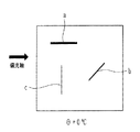
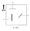
a,b,c ナノ線
Claims (6)
- 光源から発せられる光をナノ線素子用試料に提供する光源部と、
該光源部から提供された前記光の経路上に設けられ、前記光を偏光させる回転偏光板と、
該回転偏光板に電気的に連結されて該回転偏光板を第1周波数(f 0 )で回転させる偏光板制御機と、
前記ナノ線素子用試料から反射される光を検出する光学顕微鏡と、
該光学顕微鏡に設けられ、前記回転偏光板が回転する間、前記光学顕微鏡によって検出された光を撮影した映像データを貯蔵するCCDカメラと、
前記映像データのピクセルに含まれた光の強さ情報を高速フーリエ変換処理して前記映像データのピクセルのうち第2周波数(2f 0 )を有するピクセルを抽出することにより、前記ナノ線素子用試料に含まれたナノ線の映像を得るデータ処理部と
を備えたことを特徴とするナノ線感知用光学顕微鏡システム。 - 前記ナノ線は、前記ナノ線の形成方向と前記ナノ線に入射された光の偏光軸間の角度に応じて異なるように発光する光学的異方性を有することを特徴とする請求項1に記載のナノ線感知用光学顕微鏡システム。
- 前記偏光板制御機は、前記回転偏光板を0.1〜1Hzの前記第1周波数(f0 )で回転するように制御することを特徴とする請求項1に記載のナノ線感知用光学顕微鏡システム。
- 前記回転偏光板の回転により、前記ナノ線素子用試料に入射される光の偏光軸が前記第2周波数(2f0 )に変調されることを特徴とする請求項3に記載のナノ線感知用光学顕微鏡システム。
- 前記偏光軸が前記第2周波数(2f 0 )で回転された光が前記ナノ線素子用試料に入射されれば、前記ナノ線から反射された光の強さは、前記第2周波数(2f 0 )に変調されることを特徴とする請求項4に記載のナノ線感知用光学顕微鏡システム。
- 前記CCDカメラによって撮影された映像データは、時間によってピクセル配列で貯蔵され、前記データ処理部は、各ピクセルの時間別光強さ情報(I(n,m) 1 )を高速フーリエ変換して前記第2周波数(2f 0 )に対応する複素数フーリエ係数((2f 0 )n,m)を選択することで、前記ナノ線の映像を得ることを特徴とする請求項1に記載のナノ線感知用光学顕微鏡システム。
Applications Claiming Priority (4)
| Application Number | Priority Date | Filing Date | Title |
|---|---|---|---|
| KR10-2006-0122347 | 2006-12-05 | ||
| KR20060122347 | 2006-12-05 | ||
| KR1020070061460A KR100848033B1 (ko) | 2006-12-05 | 2007-06-22 | 편광판과 고속 푸리에 변환을 이용한 나노선 감지용 광학현미경 시스템 |
| KR10-2007-0061460 | 2007-06-22 |
Publications (2)
| Publication Number | Publication Date |
|---|---|
| JP2008147629A JP2008147629A (ja) | 2008-06-26 |
| JP4690379B2 true JP4690379B2 (ja) | 2011-06-01 |
Family
ID=39607415
Family Applications (1)
| Application Number | Title | Priority Date | Filing Date |
|---|---|---|---|
| JP2007285276A Expired - Fee Related JP4690379B2 (ja) | 2006-12-05 | 2007-11-01 | 偏光板と高速フーリエ変換を用いたナノ線感知用光学顕微鏡システム |
Country Status (1)
| Country | Link |
|---|---|
| JP (1) | JP4690379B2 (ja) |
Families Citing this family (14)
| Publication number | Priority date | Publication date | Assignee | Title |
|---|---|---|---|---|
| US9864184B2 (en) | 2012-10-30 | 2018-01-09 | California Institute Of Technology | Embedded pupil function recovery for fourier ptychographic imaging devices |
| US10679763B2 (en) | 2012-10-30 | 2020-06-09 | California Institute Of Technology | Fourier ptychographic imaging systems, devices, and methods |
| US10652444B2 (en) | 2012-10-30 | 2020-05-12 | California Institute Of Technology | Multiplexed Fourier ptychography imaging systems and methods |
| CN105659143B (zh) | 2013-07-31 | 2019-03-22 | 加州理工学院 | 孔径扫描傅立叶重叠关联成像 |
| WO2015027188A1 (en) | 2013-08-22 | 2015-02-26 | California Institute Of Technoloby | Variable-illumination fourier ptychographic imaging devices, systems, and methods |
| US11468557B2 (en) | 2014-03-13 | 2022-10-11 | California Institute Of Technology | Free orientation fourier camera |
| WO2016106379A1 (en) * | 2014-12-22 | 2016-06-30 | California Institute Of Technology | Epi-illumination fourier ptychographic imaging for thick samples |
| CA2970063A1 (en) | 2015-01-21 | 2016-07-28 | California Institute Of Technology | Fourier ptychographic tomography |
| EP3251144A4 (en) | 2015-01-26 | 2018-09-05 | California Institute of Technology | Array level fourier ptychographic imaging |
| JP2018509622A (ja) | 2015-03-13 | 2018-04-05 | カリフォルニア インスティチュート オブ テクノロジー | フーリエタイコグラフィ手法を用いるインコヒーレント撮像システムにおける収差補正 |
| US10568507B2 (en) | 2016-06-10 | 2020-02-25 | California Institute Of Technology | Pupil ptychography methods and systems |
| US11092795B2 (en) | 2016-06-10 | 2021-08-17 | California Institute Of Technology | Systems and methods for coded-aperture-based correction of aberration obtained from Fourier ptychography |
| US10754140B2 (en) | 2017-11-03 | 2020-08-25 | California Institute Of Technology | Parallel imaging acquisition and restoration methods and systems |
| WO2022183078A1 (en) | 2021-02-25 | 2022-09-01 | California Institute Of Technology | Computational refocusing-assisted deep learning |
Family Cites Families (4)
| Publication number | Priority date | Publication date | Assignee | Title |
|---|---|---|---|---|
| JPH0997332A (ja) * | 1995-09-29 | 1997-04-08 | Shimadzu Corp | 顕微鏡の画像処理方法 |
| JPH10104524A (ja) * | 1996-08-08 | 1998-04-24 | Nikon Corp | 微分干渉顕微鏡 |
| JPH10268200A (ja) * | 1997-03-24 | 1998-10-09 | Olympus Optical Co Ltd | 干渉顕微鏡装置 |
| JPWO2006123712A1 (ja) * | 2005-05-18 | 2008-12-25 | オリンパス株式会社 | 偏光顕微鏡 |
-
2007
- 2007-11-01 JP JP2007285276A patent/JP4690379B2/ja not_active Expired - Fee Related
Also Published As
| Publication number | Publication date |
|---|---|
| JP2008147629A (ja) | 2008-06-26 |
Similar Documents
| Publication | Publication Date | Title |
|---|---|---|
| JP2008147629A (ja) | 偏光板と高速フーリエ変換を用いたナノ線感知用光学顕微鏡システム | |
| Shi et al. | Uncovering material deformations via machine learning combined with four-dimensional scanning transmission electron microscopy | |
| Miao et al. | Single pixel black phosphorus photodetector for near‐infrared imaging | |
| Scrymgeour et al. | Polarity and piezoelectric response of solution grown zinc oxide nanocrystals on silver | |
| US11143672B2 (en) | Method and apparatus for correcting responsivity variation in photothermal imaging | |
| US12125668B2 (en) | Electron microscopy grid | |
| CN106324486A (zh) | 集成电路的光学纳米探测 | |
| KR100848033B1 (ko) | 편광판과 고속 푸리에 변환을 이용한 나노선 감지용 광학현미경 시스템 | |
| WO2008006537A1 (fr) | Procédé d'identification d'un individu | |
| Li et al. | Self-assembly of C60 monolayer on epitaxially grown, nanostructured graphene on Ru (0001) surface | |
| US11029329B2 (en) | Method of and system for detecting structures on or below the surface of a sample using a probe including a cantilever and a probe tip | |
| TW200832089A (en) | Lithography alignment system and method using nDSE-based feedback control | |
| CN111189828B (zh) | 一种旋转无透镜像素超分辨成像系统及其成像方法 | |
| JP2005530410A5 (ja) | ||
| Miranda et al. | Simultaneous differential spinning disk fluorescence optical sectioning microscopy and nanomechanical mapping atomic force microscopy | |
| Xu et al. | Bending and twisting of suspended single-walled carbon nanotubes in solution | |
| Leis et al. | Nanoscale tip positioning with a multi-tip scanning tunneling microscope using topography images | |
| WO2017197930A1 (zh) | 一种接触式图像传感器及图像扫描装置 | |
| CN106791355A (zh) | 基于图像频域拼接的单像素成像方法及系统 | |
| Tyagi et al. | Scanning tunneling microscope‐characterization of chemical vapor deposition‐graphene: ripples and twisted bi‐layers at multiple scales | |
| TWI628140B (zh) | 區分奈米碳管類型的方法 | |
| Zhao et al. | A bi-channel aided stitching of atomic force microscopy images | |
| Polomoff et al. | Single ferroelectric domain nucleation and growth monitored by high speed piezoforce microscopy | |
| Ayela et al. | Introducing a well-ordered volume porosity in 3-dimensional gold microcantilevers | |
| Vlasin et al. | Optical imaging of nonuniform ferroelectricity and strain at the diffraction limit |
Legal Events
| Date | Code | Title | Description |
|---|---|---|---|
| A131 | Notification of reasons for refusal |
Free format text: JAPANESE INTERMEDIATE CODE: A131 Effective date: 20100917 |
|
| A521 | Request for written amendment filed |
Free format text: JAPANESE INTERMEDIATE CODE: A523 Effective date: 20101215 |
|
| TRDD | Decision of grant or rejection written | ||
| A01 | Written decision to grant a patent or to grant a registration (utility model) |
Free format text: JAPANESE INTERMEDIATE CODE: A01 Effective date: 20110204 |
|
| A01 | Written decision to grant a patent or to grant a registration (utility model) |
Free format text: JAPANESE INTERMEDIATE CODE: A01 |
|
| A61 | First payment of annual fees (during grant procedure) |
Free format text: JAPANESE INTERMEDIATE CODE: A61 Effective date: 20110217 |
|
| R150 | Certificate of patent or registration of utility model |
Ref document number: 4690379 Country of ref document: JP Free format text: JAPANESE INTERMEDIATE CODE: R150 Free format text: JAPANESE INTERMEDIATE CODE: R150 |
|
| FPAY | Renewal fee payment (event date is renewal date of database) |
Free format text: PAYMENT UNTIL: 20140225 Year of fee payment: 3 |
|
| R250 | Receipt of annual fees |
Free format text: JAPANESE INTERMEDIATE CODE: R250 |
|
| R250 | Receipt of annual fees |
Free format text: JAPANESE INTERMEDIATE CODE: R250 |
|
| R250 | Receipt of annual fees |
Free format text: JAPANESE INTERMEDIATE CODE: R250 |
|
| R250 | Receipt of annual fees |
Free format text: JAPANESE INTERMEDIATE CODE: R250 |
|
| R250 | Receipt of annual fees |
Free format text: JAPANESE INTERMEDIATE CODE: R250 |
|
| S111 | Request for change of ownership or part of ownership |
Free format text: JAPANESE INTERMEDIATE CODE: R313117 |
|
| S531 | Written request for registration of change of domicile |
Free format text: JAPANESE INTERMEDIATE CODE: R313531 |
|
| R350 | Written notification of registration of transfer |
Free format text: JAPANESE INTERMEDIATE CODE: R350 |
|
| R350 | Written notification of registration of transfer |
Free format text: JAPANESE INTERMEDIATE CODE: R350 |
|
| R250 | Receipt of annual fees |
Free format text: JAPANESE INTERMEDIATE CODE: R250 |
|
| R250 | Receipt of annual fees |
Free format text: JAPANESE INTERMEDIATE CODE: R250 |
|
| R250 | Receipt of annual fees |
Free format text: JAPANESE INTERMEDIATE CODE: R250 |
|
| LAPS | Cancellation because of no payment of annual fees |