JP4679268B2 - Light emitting diode composite element - Google Patents
Light emitting diode composite element Download PDFInfo
- Publication number
- JP4679268B2 JP4679268B2 JP2005189733A JP2005189733A JP4679268B2 JP 4679268 B2 JP4679268 B2 JP 4679268B2 JP 2005189733 A JP2005189733 A JP 2005189733A JP 2005189733 A JP2005189733 A JP 2005189733A JP 4679268 B2 JP4679268 B2 JP 4679268B2
- Authority
- JP
- Japan
- Prior art keywords
- light emitting
- emitting diode
- submount
- light
- composite element
- Prior art date
- Legal status (The legal status is an assumption and is not a legal conclusion. Google has not performed a legal analysis and makes no representation as to the accuracy of the status listed.)
- Expired - Fee Related
Links
Images

Landscapes
- Led Device Packages (AREA)
Description
本発明は、光学特性が同種又は異種のフリップチップ型の発光ダイオードをサブマウント上に配置接続し、印刷配線基板に取り付けるようにした表面実装型パッケージである発光ダイオード複合素子に関するものである。 The present invention relates to a light-emitting diode composite element which is a surface-mount package in which flip-chip light-emitting diodes having the same or different optical characteristics are arranged and connected on a submount and attached to a printed wiring board.
特に、本発明は、発光ダイオードを近接して配置することにより、色むらの少ない高輝度の光源が容易に得られる発光ダイオード複合素子に関するものである。 In particular, the present invention relates to a light emitting diode composite element in which a light source with high luminance and less color unevenness can be easily obtained by arranging light emitting diodes close to each other.
たとえば、特許文献1に記載されている半導体発光装置は、薄型化を図るために、保持基板の裏面にサブマウントの厚みと同等のサブマウント収納用凹部を形成し、前記サブマウント収納用凹部に前記サブマウントを収納した状態で、前記サブマウントの電極のそれぞれと保持基板の配線を接続している。
For example, in the semiconductor light emitting device described in
また、特許文献2に記載されている複合発光素子は、サブマウントの配線とフリプチップ型発光ダイオードの電極とをバンプを介して接続している。 In the composite light emitting device described in Patent Document 2, the submount wiring and the flip chip type light emitting diode electrode are connected via bumps.
さらに、特許文献3に記載されている表面実装型発光ダイオードは、鉛を使用しない金−錫ハンダを使用して発光ダイオードを実装している。
Furthermore, the surface-mounted light-emitting diode described in
発光層からの光を電極の反対側の面から取り出すフリップチップ型の発光ダイオードは、電極による光の遮りがないため明るく、発光効率が良い。しかし、フリップチップ型の発光ダイオードの電極は、サブマウント上の配線と金線を介して接続するか、あるいは前記配線上に載置されたハンダバンプにより接続されていた。 A flip-chip light emitting diode that extracts light from the light emitting layer from the surface opposite to the electrode is bright and has high light emission efficiency because the light is not blocked by the electrode. However, the electrodes of the flip chip type light emitting diode are connected to the wiring on the submount via a gold wire, or are connected by solder bumps placed on the wiring.
発光ダイオードの電極とサブマウント上の配線とを金線で接続するのは、通常、自動機を用いて行われるが、熱サイクルにより接続部の寿命が短縮されるなど、信頼性に問題があった。また、ハンダバンプによる接続は、フラックス成分が飛散するとともに、温度を上げると、発光ダイオードの重みでハンダバンプが薄くなり、接合部が広がったり、あるいはハンダの一部が溶けて流出し、配線間の短絡を起こす恐れがあった。このようなハンダの広がりや流出を防止するために、その近傍に絶縁膜を配し、配線における短絡を防いでいた。 The connection of the LED electrode and the wiring on the submount with a gold wire is usually performed using an automatic machine. However, there is a problem in reliability, such as shortening the life of the connection part due to thermal cycling. It was. In addition, solder bump connection causes the flux components to scatter, and when the temperature is raised, the solder bumps become thinner due to the weight of the light emitting diode, the joints spread, or a part of the solder melts and flows out, causing a short circuit between the wirings. There was a risk of causing. In order to prevent such spread and outflow of the solder, an insulating film is provided in the vicinity thereof to prevent a short circuit in the wiring.
ハンダバンプによる発光ダイオードとサブマウントにおける配線との接続は、使用中に発生する熱により膨張するため、接続部分が剥がれたり、発光ダイオードが破壊され易いという欠点がある。また、従来の発光ダイオードは、それぞれが持つ特有の色を発生するが、その中間色や色調を変えることが困難であった。 Since the connection between the light emitting diode and the wiring on the submount by the solder bump expands due to heat generated during use, there is a drawback that the connection portion is peeled off or the light emitting diode is easily destroyed. Further, the conventional light emitting diodes generate their own unique colors, but it is difficult to change their intermediate colors and tone.
本発明は、上記問題点を解消するためになされたものであり、発光ダイオードを近接して配置してもハンダの広がりや流出による配線間の短絡を防止することができる発光ダイオード複合素子を提供することを目的とする。 The present invention has been made to solve the above-described problems, and provides a light-emitting diode composite element capable of preventing a short circuit between wires due to spread of solder or outflow even when light-emitting diodes are arranged close to each other. The purpose is to do.
本発明は、発光ダイオードを近接して配置することにより、異なる色の光がよく混ざり、色むらが少なく、かつ、色調を自在に変えることができるフルカラー光源、あるいは、単色の高輝度光源が容易に得られる発光ダイオード複合素子を提供することを目的とする。 In the present invention, by arranging the light emitting diodes close to each other, light of different colors is well mixed, color unevenness is small, and a full color light source that can freely change the color tone or a monochromatic high-intensity light source is easy. It aims at providing the light emitting diode composite element obtained in this.
本発明者は、鋭意研究を重ねた結果、発光ダイオードの電極とサブマウント上の配線とを高融点の共晶ハンダを介して接続し、また、発光ダイオードを搭載したサブマウントを収納した架台上の配線とサブマウント上の配線とを比較的低い温度で硬化又は溶融する接着剤又は共晶ハンダを介して接続するとともに、サブマウント上に発光ダイオードを特定の配置形状で搭載することにより、上記課題が解決できることを見出し、本発明を完成した。 As a result of intensive research, the present inventor has connected the electrode of the light emitting diode and the wiring on the submount through a high melting point eutectic solder, and also on the gantry containing the submount on which the light emitting diode is mounted. By connecting the wiring on the submount and the wiring on the submount via an adhesive or eutectic solder that cures or melts at a relatively low temperature, and mounting the light emitting diode on the submount in a specific arrangement shape, The present invention has been completed by finding out that the problems can be solved.
(第1発明)
すなわち、本発明の要旨は、
上面に上中下3段に並列する3対の配線が形成され、フリップチップ型の発光ダイオードの各電極が金80%、錫20%からなる第1の共晶ハンダを介して前記3対の配線に接続されており、中段に位置する1対の配線に前記発光ダイオードが1つ接続され、上下2段に位置する各1対の配線に前記発光ダイオードがそれぞれ各2つずつ直列に接続されているサブマウントと、
上面側中心部に前記サブマウントが収納される空所が設けられるとともに両側に各3つの上下貫通孔が設けられ、前記空所の端縁から上面と各上下貫通孔の内面を経由して下面まで連通する配線が3対形成された架台と、
前記架台上に前記サブマウントに搭載された前記発光ダイオードを取り囲むように形成される発光反射筒と、
前記発光反射筒の内側に透明樹脂を充填して形成される発光ダイオード封止体とから構成され、
前記架台の上面に形成された各配線の前記空所側端子が、導電性熱硬化性接着剤又は融点が120〜230℃の範囲にある第2の共晶ハンダを介して、前記サブマウント上に形成された各配線の前記サブマウント周縁側端子にそれぞれ接続されていることを特徴とする発光ダイオード複合素子
にある。
(First invention)
That is, the gist of the present invention is as follows.
Three pairs of wirings are formed on the upper surface in parallel with the upper, middle, and lower three stages, and each of the electrodes of the flip-chip type light emitting diode is formed of the three pairs through a first eutectic solder made of 80% gold and 20% tin. One light emitting diode is connected to a pair of wires located in the middle stage, and two light emitting diodes are connected in series to each pair of wires located in the upper and lower two stages. With a submount,
A space for storing the submount is provided at the center on the upper surface side, and three upper and lower through holes are provided on both sides, and the lower surface from the edge of the space via the upper surface and the inner surfaces of the upper and lower through holes. A gantry in which three pairs of wires communicating with each other are formed;
A light-emitting reflection tube formed on the base so as to surround the light-emitting diode mounted on the submount;
A light emitting diode sealing body formed by filling a transparent resin inside the light emitting reflecting cylinder,
The void-side terminal of each wiring formed on the upper surface of the gantry is connected to the submount through a conductive thermosetting adhesive or a second eutectic solder having a melting point in the range of 120 to 230 ° C. The light-emitting diode composite element is connected to the peripheral terminal of the submount of each wiring formed on the substrate.
(第2発明)
第1発明の発光ダイオード複合素子において、
前記中段に位置する1対の配線に接続される前記発光ダイオードの発光色が赤色であり、前記上下2段に位置する各1対の配線に接続される前記発光ダイオードの発光色のいずれか一方が緑色であり、他方が青色であることを特徴とする。
(Second invention)
In the light emitting diode composite element of the first invention,
The light emitting color of the light emitting diode connected to the pair of wirings located in the middle stage is red, and one of the light emitting colors of the light emitting diodes connected to the pair of wirings located in the two upper and lower stages Is green and the other is blue.
(第3発明)
第1発明又は第2発明の発光ダイオード複合素子において、
前記発光ダイオードが制御回路によって点滅制御されることを特徴とする。
(Third invention)
In the light emitting diode composite element of the first invention or the second invention,
The light emitting diode is controlled to blink by a control circuit.
(第4発明)
第1発明から第3発明のいずれかの発光ダイオード複合素子において、
前記発光ダイオードの電極に印加する電圧を変えることにより、全体の色調を特定色に調整することを特徴とする。
(Fourth invention)
In the light-emitting diode composite element according to any one of the first to third inventions,
The overall color tone is adjusted to a specific color by changing the voltage applied to the electrode of the light emitting diode.
(第5発明)
第1発明の発光ダイオード複合素子において、
前記発光ダイオードが発光色の同じ1種類からなることを特徴とする。
(Fifth invention)
In the light emitting diode composite element of the first invention,
The light emitting diode is characterized by comprising one kind of the same luminescent color.
本発明によれば、発光ダイオードの電極とサブマウント上の配線とを高融点の金錫共晶ハンダを介して接続し、また、架台上の配線とサブマウント上の配線とを比較的低い温度で硬化する導電性熱硬化性接着剤又は比較的低融点の共晶ハンダを介して接続するため、比較的低温で行われる配線接続の際に、前記金錫共晶ハンダが溶融して広がり、隣の配線と短絡するおそれがない。したがって、発光ダイオードを近接して配置することができる。 According to the present invention, the electrode of the light emitting diode and the wiring on the submount are connected via the high melting point gold-tin eutectic solder, and the wiring on the gantry and the wiring on the submount are connected at a relatively low temperature. In order to connect via a conductive thermosetting adhesive or a relatively low melting point eutectic solder that cures at the time of wiring connection performed at a relatively low temperature, the gold-tin eutectic solder melts and spreads, There is no risk of short circuiting with adjacent wiring. Therefore, the light emitting diodes can be arranged close to each other.
本発明によれば、発光ダイオードを近接して配置することができるので、異なる色の光がよく混ざり、色むらが少なく、かつ、色調を自在に変えることができるフルカラー光源、あるいは、単色の高輝度光源が容易に得られる。 According to the present invention, since the light emitting diodes can be arranged close to each other, the light of different colors is well mixed, the color unevenness is small, and the color tone can be freely changed. A luminance light source can be easily obtained.
本発明によれば、発光ダイオードの電極とサブマウント上の配線との接触面積を金線より大きくとることができるため、これらの接続強度を大きくすることが可能であるだけでなく、発光ダイオードから発生する熱をサブマウントおよび印刷配線基板を介して外部に逃がすことができ、経年変化による不良や劣化を防止することができる。 According to the present invention, since the contact area between the electrode of the light emitting diode and the wiring on the submount can be made larger than that of the gold wire, it is possible not only to increase the connection strength but also from the light emitting diode. The generated heat can be released to the outside through the submount and the printed wiring board, and defects and deterioration due to secular change can be prevented.
(第1発明)
第1発明においては、サブマウント基板として、耐熱性と熱伝導性の良好なセラミックなどの電気絶縁性材料、たとえば、窒化アルミニウムからなる板状体を用い、その上に、サブマウント上に形成される上中下3段に並列する3対の配線及び2つのフリップチップ型の発光ダイオードを直列に接続するための2つの配線からなる1組の配線群を多数形成する。配線パターン(回路)の形成は通常のプリント配線の手法による。そして、前記サブマウント基板に形成された多数の配線上には、金80%、錫20%からなる第1の共晶ハンダを用いて各配線の所定位置に前記第1の共晶ハンダからなる層を形成する。
(First invention)
In the first invention, an electrical insulating material such as ceramic having good heat resistance and thermal conductivity, for example, a plate-like body made of aluminum nitride is used as the submount substrate, and the submount substrate is formed on the submount. A large number of one set of wiring groups are formed, each consisting of three pairs of wirings arranged in three upper and lower middle stages and two wirings for connecting two flip-chip type light emitting diodes in series. The wiring pattern (circuit) is formed by a normal printed wiring method. Then, a first eutectic solder made of 80% gold and 20% tin is used to form the first eutectic solder at a predetermined position on each wiring on the submount substrate. Form a layer.
次いで、光学特性が同種又は異種のフリップチップ型の発光ダイオードの電極を前記第1の共晶ハンダからなる層上に配置した後、発光ダイオードが搭載されたサブマウント基板をリフロー炉で加熱することにより、発光ダイオードの電極を前記第1の共晶ハンダを介してサブマウント基板に形成された配線と接続する。その後、サブマウント基板をダイシングし、前記1組の配線群上に発光ダイオードが搭載されたサブマウントを多数製作する。なお、前記第1の共晶ハンダの融点は300℃に近い高温である。 Next, after disposing the electrodes of the flip chip type light emitting diode of the same kind or different kinds of optical characteristics on the layer made of the first eutectic solder, the submount substrate on which the light emitting diode is mounted is heated in a reflow furnace. Thus, the electrode of the light emitting diode is connected to the wiring formed on the submount substrate through the first eutectic solder. Thereafter, the submount substrate is diced to produce a large number of submounts in which light emitting diodes are mounted on the one set of wiring groups. The melting point of the first eutectic solder is a high temperature close to 300 ° C.
一方、サブマウントを収納する架台は、サブマウント基板の材料と同様のセラミック材料、たとえば、窒化アルミニウムやアルミナからなり、上面側中心部に空所が設けられるとともに両側に各3つの上下貫通孔が設けられる。また、架台には、前記空所の端縁から上面と各上下貫通孔の内面を経由して下面まで連通する配線が3対形成される。このようにして製作した架台の空所に前記サブマウントを収納する。 On the other hand, the gantry for storing the submount is made of a ceramic material similar to the material of the submount substrate, for example, aluminum nitride or alumina, and a space is provided in the center on the upper surface side, and three upper and lower through holes are provided on both sides. Provided. In addition, three pairs of wirings are formed on the frame so as to communicate from the edge of the void to the lower surface via the upper surface and the inner surfaces of the upper and lower through holes. The submount is housed in a space of the gantry thus manufactured.
なお、発光ダイオードからの発熱を印刷配線基板側に逃がすため、サブマウントをヒートシンク上に設置することが望ましく、前記架台の下面側の中央部に凹溝を形成し、これにヒートシンクを収納すればよい。ヒートシンクは多数の放熱用フィンを有する構造のものが望ましく、その材質の好適例として、銅又はアルミニウムからなる構造体の表面にニッケルメッキを施したものが挙げられる。 In order to release heat from the light emitting diode to the printed wiring board side, it is desirable to install the submount on the heat sink, and if a concave groove is formed in the central part on the lower surface side of the gantry and the heat sink is accommodated in this Good. The heat sink preferably has a structure having a large number of heat-dissipating fins, and a suitable example of the material is one in which the surface of a structure made of copper or aluminum is plated with nickel.
架台の上面に形成された配線の前記空所側端子は、導電性熱硬化性接着剤又は融点が120〜230℃の範囲にある第2の共晶ハンダを介して、前記サブマウントに形成された配線のサブマウント周縁側端子にそれぞれ接続される。 The void-side terminal of the wiring formed on the upper surface of the gantry is formed on the submount through a conductive thermosetting adhesive or a second eutectic solder having a melting point in the range of 120 to 230 ° C. Are connected to the terminals on the peripheral edge of the submount.
架台上に発光ダイオードから発する光を内面で反射する発光反射筒を設置する。発光反射筒は、架台の材料と同様のセラミック材料、シリコン樹脂に酸化チタンやアルミナの粉末を充填した材料などを用いて、逆円錐台筒形状に成形する。架台上に設置した発光反射筒の内側に透明樹脂を充填し、サブマウントに搭載した発光ダイオードを封止する発光ダイオード封止体を形成する。 A light-emitting reflection cylinder that reflects light emitted from the light-emitting diode on the inner surface is installed on the gantry. The light-emitting reflection cylinder is formed into an inverted truncated cone shape using a ceramic material similar to the material of the gantry or a material in which a silicon resin is filled with titanium oxide or alumina powder. A light-emitting diode sealing body is formed by filling a transparent resin inside the light-emitting reflection cylinder installed on the gantry and sealing the light-emitting diode mounted on the submount.
以上のようにして組み立てられた発光ダイオード複合素子は、印刷配線基板上に多数配置され、各素子の架台下面に形成された配線端子が印刷配線基板上に形成されているプリント配線に接続される。このようにして発光ダイオード複合素子の集合体が形成される。 A large number of light emitting diode composite elements assembled as described above are arranged on a printed wiring board, and wiring terminals formed on the bottom surface of each element are connected to printed wiring formed on the printed wiring board. . In this way, an aggregate of light emitting diode composite elements is formed.
第1発明の発光ダイオード複合素子においては、サブマウント上の配線と発光ダイオードの電極とが高融点の第1の共晶ハンダによって接続される一方、架台上面に形成された配線とサブマウント上の配線とは、第1の共晶ハンダの融点より低い温度で硬化する導電性熱硬化性接着剤、又は融点が第1の共晶ハンダの融点より低い第2の共晶ハンダによって後から接続される。したがって、サブマウント上の配線と発光ダイオードの電極との接続箇所は、後の接続時の加熱によってハンダが融解することがなく、堅固な接続が維持される。 In the light emitting diode composite element of the first invention, the wiring on the submount and the electrode of the light emitting diode are connected by the high melting point first eutectic solder, while the wiring formed on the gantry upper surface and the submount The wiring is connected later by a conductive thermosetting adhesive that cures at a temperature lower than the melting point of the first eutectic solder, or a second eutectic solder whose melting point is lower than the melting point of the first eutectic solder. The Therefore, the connection portion between the wiring on the submount and the electrode of the light emitting diode does not melt the solder due to heating at the time of subsequent connection, and a firm connection is maintained.
第1発明の発光ダイオード複合素子は、サブマウントに形成された配線と発光ダイオードの電極との接続に金線またはハンダバンプを使用しないため、熱変化に強くまたハンダ付けの際に広がらなく、配線間の短絡を防止することができる。 The light-emitting diode composite element of the first invention does not use gold wires or solder bumps for connection between the wiring formed on the submount and the electrode of the light-emitting diode, so it is resistant to thermal changes and does not spread during soldering. Can be prevented.
第1発明の発光ダイオード複合素子において、発光ダイオードの電極とサブマウント上の配線との接続に用いる第1の共晶ハンダは、蒸着法、スクリーン印刷法又はメッキ法により薄い箔状に形成するか、薄い箔状に形成したものを載置して用いる。前記第1の共晶ハンダからなる層は、所望の厚さで、しかも均一に形成されるため、サブマウント上の配線と発光ダイオードの電極とが安定して接続される。 In the light-emitting diode composite element of the first invention, is the first eutectic solder used for connection between the electrode of the light-emitting diode and the wiring on the submount formed in a thin foil shape by vapor deposition, screen printing, or plating? A thin foil is used. The layer made of the first eutectic solder has a desired thickness and is uniformly formed, so that the wiring on the submount and the electrode of the light emitting diode are stably connected.
第1発明の発光ダイオード複合素子は、印刷配線基板上にマトリクス状又はその他の所望の形状に配置され、前記架台の下面に形成された配線が前記印刷配線基板上に形成された配線に接続されているため、画像として掲示板、広告装置、方向表示装置、信号装置、その他各種表示装置に利用することができる。 The light-emitting diode composite element of the first invention is arranged in a matrix or other desired shape on the printed wiring board, and the wiring formed on the lower surface of the gantry is connected to the wiring formed on the printed wiring board. Therefore, it can be used as an image for a bulletin board, an advertising device, a direction display device, a signal device, and other various display devices.
(第2発明)
第2発明の発光ダイオード複合素子は、サブマウントの中段の中央に赤色の発光ダイオードを1つ、上下段に緑色と青色の発光ダイオードを各2つずつ配置したので、異なる色の光がよく混ざり、色むらが少なく、かつ、色調を自在に変えることができるフルカラー光源が容易に得られる。
(Second invention)
In the light emitting diode composite element of the second invention, one red light emitting diode is arranged at the center of the middle stage of the submount, and two green and blue light emitting diodes are arranged on the upper and lower stages, so that light of different colors are mixed well. Thus, a full-color light source that has little color unevenness and can freely change the color tone can be easily obtained.
(第3発明)
第3発明の発光ダイオード複合素子は、印刷配線基板上のプリント配線に接続された制御回路によって少なくとも2種類からなる発光ダイオードの点滅制御が行われるため、文字や画像を動かすことができる。また、第3発明の発光ダイオード複合素子は、たとえば、赤色の発光ダイオード、橙色の発光ダイオード、青色の発光ダイオードの三色をそれぞれ複数個並べ、それぞれの電圧を制御することで、強い赤色、薄い緑色、白色に近い赤色等、色調を各種制御することができる。
(Third invention)
In the light-emitting diode composite element according to the third aspect of the invention, the blinking control of at least two types of light-emitting diodes is performed by a control circuit connected to the printed wiring on the printed wiring board, so that characters and images can be moved. The light-emitting diode composite element according to the third aspect of the invention is, for example, a strong red, thin by arranging a plurality of three colors, a red light-emitting diode, an orange light-emitting diode, and a blue light-emitting diode, and controlling the respective voltages. Various color tones such as green and red close to white can be controlled.
第1〜第3発明の発光ダイオード複合素子は、発光ダイオードの色を赤色、黄色、橙色、緑色、青色の内、たとえば、2種類又は3種類とし、複数個配置することにより、また電圧の印加を調整することにより動画像等を表示することができる。また、第1〜第5発明の発光ダイオード複合素子は、少なくとも2種類からなる発光ダイオードを、赤色、黄色、橙色、緑色、青色の内から選択し、異なる色を発光する複数種類を印刷配線基板に配置することにより、画像に適した色調を表すことができる。 In the light-emitting diode composite element according to the first to third inventions, the color of the light-emitting diode is red, yellow, orange, green or blue, for example, two or three kinds, and a plurality of them are arranged, and a voltage is applied. A moving image or the like can be displayed by adjusting. In the light-emitting diode composite element according to the first to fifth inventions, at least two types of light-emitting diodes are selected from red, yellow, orange, green, and blue, and a plurality of types that emit different colors are printed wiring boards. By arranging in the above, it is possible to represent a color tone suitable for an image.
(第4発明)
第4発明の発光ダイオード複合素子は、たとえば、赤色、緑色及び青色の発光ダイオードが内蔵され、それぞれの電極に印加する電圧を変えることにより、全体の色調を調整することができ、赤色や黄色にすることにより自動車のウインカーとして使用できる。
(Fourth invention)
The light-emitting diode composite element of the fourth invention includes, for example, red, green, and blue light-emitting diodes, and the overall color tone can be adjusted by changing the voltage applied to each electrode. By doing so, it can be used as a turn signal for automobiles.
第4発明の発光ダイオード複合素子は、白色光又は橙色光を作製することができる。白色光は、制御回路により点滅を行うことにより、見易い文字を表示することができ、また、橙色光は、赤色と交互に発光することで信号機とすることができる。 The light-emitting diode composite element of the fourth invention can produce white light or orange light. White light can be blinked by a control circuit to display easy-to-see characters, and orange light can be used as a traffic light by emitting light alternately with red.
第4発明の発光ダイオード複合素子は、2種類または3種類からなる発光ダイオードが内蔵された複数個の複合素子を、たとえば、赤色の領域用と橙色の領域用とを作製しておき、これらを組み合わせて自動車のウインカーのような信号灯として使用することができる。 The light-emitting diode composite element according to the fourth aspect of the present invention is a composite element in which two or three types of light-emitting diodes are built, for example, for a red region and an orange region. In combination, it can be used as a signal light like an automobile blinker.
第4発明の発光ダイオード複合素子は、2種類または3種類からなる発光ダイオードが内蔵された複数個の複合素子がそれぞれの電極に印加する電圧を変えて赤色の領域、橙色の領域、および青色の領域を作製し、たとえば、道路等の信号機として使用することができる。 A light emitting diode composite element according to a fourth aspect of the present invention includes a red region, an orange region, and a blue region by changing a voltage applied to each electrode by a plurality of composite devices each including two or three types of light emitting diodes. An area can be created and used, for example, as a traffic light on a road or the like.
第1発明から第4発明の発光ダイオード複合素子は、2種類または3種類からなる発光ダイオードが内蔵され、発光部をサブマウントの中心に集め、電極を端部に配置することにより、光のバランスを良くすることができ、発光部の明るさのムラを無くすことができる。 The light-emitting diode composite elements according to the first to fourth aspects of the present invention incorporate two or three types of light-emitting diodes, collect the light-emitting portions at the center of the submount, and arrange the electrodes at the ends to balance the light. Can be improved, and unevenness in the brightness of the light emitting portion can be eliminated.
(第5発明)
第5発明の発光ダイオード複合素子は、サブマウント上に発光色の同じ発光ダイオードを配置することにより、従来のものと比べて高輝度の光源が得られる。
(Fifth invention)
In the light emitting diode composite element according to the fifth aspect of the present invention, a light source having higher luminance than that of the conventional one can be obtained by disposing light emitting diodes having the same emission color on the submount.
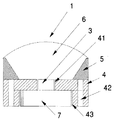
図1〜図3は、いずれも本発明の実施例に係る発光ダイオード複合素子を説明するために示す図であり、図1は発光ダイオード複合素子の基本構造を示す概略縦断面図であり、図2は発光ダイオード複合素子に用いられる架台の平面図であり、図3は発光ダイオードが搭載されたサブマウントの平面図である。
図1〜図3において、発光ダイオード複合素子1は、印刷配線基板(図示されていない)上に多数個が所望の配置形状に配置接続され、発光色の異なる3種類のフリップチップ型の発光ダイオード2を搭載したサブマウント3と、上面側の中心部に形成された空所にサブマウント3を収納した架台4と、架台4上に設置形成された発光反射筒5と、発光反射筒5の内側に透明樹脂を充填して形成された発光ダイオード封止体6とから構成されている。また、架台4の下面側の中央部に形成された凹溝にヒートシンク7が収納されており、発光ダイオード2からの発熱を印刷配線基板側に逃がす役割を果たしている。なお、発光ダイオード2は、赤色の発光ダイオード21、緑色の発光ダイオード22、青色の発光ダイオード23の3種類である。
1 to 3 are views for explaining a light-emitting diode composite element according to an embodiment of the present invention, and FIG. 1 is a schematic longitudinal sectional view showing a basic structure of the light-emitting diode composite element. 2 is a plan view of a gantry used for the light emitting diode composite element, and FIG. 3 is a plan view of a submount on which the light emitting diode is mounted.
1 to 3, a light emitting diode
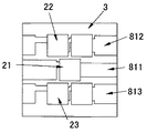
サブマウント3は、その上に配線が形成できる電気絶縁性材料から構成されるものであれば特に限定されないが、本実施例においては、熱伝導性と耐熱性に優れたセラミックである窒化アルミニウムを材料とし、板状に焼結したものが使用されている。サブマウント3上には、マスクを形成し、金を蒸着することによってサブマウント3の上面に上中下3段に並列する3対の配線81が形成されている。配線81には発光ダイオード2の各電極が金80%、錫20%からなる第1の共晶ハンダを介して接続されている。この第1の共晶ハンダは、蒸着法、スクリーン印刷法、メッキ法等により層状に形成され、その上にフラックスを予め塗布する。
前記配線の厚さは1μmから5μm程度が好ましく、前記共晶ハンダの厚さは0.2μmから0.5μm程度が好ましい。なお、中段に位置する1対の配線811には赤色の発光ダイオード21が1つ接続され、上段に位置する1対の配線812には緑色の発光ダイオード22が、下段に位置する1対の配線813には青色の発光ダイオード23がそれぞれ各2つずつ直列に接続されている。
The
The thickness of the wiring is preferably about 1 μm to 5 μm, and the thickness of the eutectic solder is preferably about 0.2 μm to 0.5 μm. One red
架台4は、サブマウント3の材料と同じ窒化アルミニウムを材料とした焼結体が用いられ、上面側中心部にサブマウント3が収納される空所41が設けられるとともに両側に各3つの上下貫通孔42が設けられ、空所41の端縁から上面と各上下貫通孔42の内面を経由して下面まで連通する配線82が3対(821、822、823)形成されている。
The
発光反射筒5は、サブマウント3や架台4の材料と同じ窒化アルミニウムを材料とした焼結体が用いられ、前記3種類からなる発光ダイオード21ないし23から発する光を内面で反射する。
The light-emitting
発光ダイオード封止体6は、エポキシ樹脂を主成分とした熱硬化性樹脂で、透明性および耐熱性に優れたものが選択され、平板状または凸レンズ状に形成する。
The light-emitting
ヒートシンク7は銅又はアルミニウムからなり、下側に多数の放熱用フィンを有し、表面にニッケルメッキが施されている。
The
次に、発光ダイオード複合素子の組立方法を説明する。サブマウント3の基板上に、配線811ないし813を一組とする配線群を多数形成する。そして、配線811ないし813上に、金80%、錫20%からなる第1の共晶ハンダを所定の位置に所定量、たとえば、ロボット等により自動的に箔の形で載置するか、蒸着する。
Next, a method for assembling the light emitting diode composite element will be described. On the substrate of the
第1の共晶ハンダ上には、異なる色の3種類からなる発光ダイオード21ないし23の電極を配置した後、リフロー炉を通過させて、発光ダイオード21ないし23とサブマウント3上に設けられた前記配線とを接続する。
On the first eutectic solder, electrodes of three kinds of
前記リフロー炉内における共晶ハンダペーストは、後述する割合になっているため、加熱によりフラックスが発散した際に、前記ハンダが広がって、配線間で短絡を起こすことがない。 Since the eutectic solder paste in the reflow furnace has a ratio described later, when the flux is diffused by heating, the solder spreads and does not cause a short circuit between the wirings.
その後、サブマウント3の基板は、発光ダイオード21ないし23を一組としてダイシングされ、多数のサブマウント3が作製される。サブマウント3に搭載された個々の発光ダイオード21ないし23は、検査装置により検査が行われて良品と不良品に選別される。
Thereafter, the substrate of the
一方、架台4には、上面側中心部に空所41を設けるとともに両側に各3つの上下貫通孔42を設け、さらに、下面側中央部に凹溝43を設ける。架台4の表面には、空所41の端縁から上面と各上下貫通孔42の内面を経由して下面まで連通する配線82を3対形成する。
On the other hand, the
次いで、架台4の凹溝43内にヒートシンク7を装着するとともに、発光ダイオード21ないし23を搭載したサブマウント3を架台4の空所41に収納し、ヒートシンク7上に設置する。サブマウント3と架台4とは上面が面一になっている。
Next, the
架台4の上面に形成された配線821ないし822は、空所41側端子を、たとえば、エポキシ系樹脂と銀粒子等を主成分とする導電性熱硬化性接着剤又は融点が120〜230℃の範囲にある第2の共晶ハンダを介して、サブマウント3上に形成された配線811ないし812のサブマウント3周縁側端子にそれぞれ接続する。また、架台4上に発光ダイオード21ないし23から発する光を内面で反射する発光反射筒5を形成するとともに、発光反射筒5の内側に透明樹脂を充填して所望の配光特性を有する発光ダイオード封止体6を形成し、発光ダイオード21ないし23を封止する。発光ダイオード封止体6の形状は、使用目的に合わせて平板状、あるいは凸レンズ状とする。
The wirings 821 to 822 formed on the upper surface of the
以上のようにして組み立てられた発光ダイオード複合素子1の印刷配線基板への接続は、架台4の下面に形成された配線端子を印刷配線基板上に施されているプリント配線に接続する。印刷配線基板上には、発光ダイオード21ないし23を点灯させるための制御回路(図示されていない)と接続するプリント配線(図示されていない)がエッチング等により所望のパターンに形成されており、印刷配線基板上に、使用目的に合わせて、一列、マトリクス状、あるいは他の形状に発光ダイオード複合素子1を配列した後、必要に応じて、全体を透明樹脂によって覆う。
The light emitting diode
本実施例で使用した金80%、錫20%からなる第1の共晶ハンダを用い、フリップチップ型の発光ダイオードの電極とサブマウント上の配線端子(電極)との接合強度を試験試料10個について測定したところ、試験試料の平均接合強度は約600gであった。なお、上記接合強度の試験は、1つの発光ダイオードにつき4箇所接合し、1箇所の接合面積は約70μmφとした。 Using the first eutectic solder made of 80% gold and 20% tin used in this example, the bonding strength between the electrode of the flip-chip type light emitting diode and the wiring terminal (electrode) on the submount was tested 10. When measured for individual pieces, the average bonding strength of the test sample was about 600 g. In the test of the bonding strength, four light emitting diodes were bonded at four positions, and the bonding area at one position was about 70 μmφ.
これに対して、接合材料を金線として超音波加熱による従来の金バンプ方式で接合した以外は、上記試験と同様にして接合部の強度を測定したところ、平均接合強度は約300gであり、上記の試験結果と比較して、約1/2の強度であった。 On the other hand, when the strength of the joint was measured in the same manner as the above test except that the joining material was joined as a gold wire by the conventional gold bump method by ultrasonic heating, the average joining strength was about 300 g. Compared with the above test results, the strength was about ½.
次に、本発明において用いられる第1の共晶ハンダ及び第2の共晶ハンダの実例を以下に挙げる。なお、金属成分の前に付した数字はSnに対するパーセンテージを表す。
第1の共晶ハンダ 溶融温度
Sn−80Au 280℃
第2の共晶ハンダ
Sn−0.75Cu 227℃
Sn−3.5Ag 221℃
Sn−0.7Ag−0.3Cu 217℃〜227℃
Sn−3.5Ag−0.75Cu 217℃〜219℃
Sn−2.5Ag−0.5Cu−1.0Bi 214℃〜221℃
Sn−2.0Ag−0.5Cu−2.0Bi 211℃〜221℃
Sn−2.5Ag−2.5Bi−2.5In 190℃〜210℃
Sn−3.5Ag−3.0Bi−6.0In 165℃〜206℃
Sn−9.0Zn 199℃
Sn−58Bi 139℃
Sn−8.0Zn−3.0Bi 187℃〜199℃
Next, actual examples of the first eutectic solder and the second eutectic solder used in the present invention will be given below. In addition, the number attached | subjected before the metal component represents the percentage with respect to Sn.
First eutectic solder melting temperature Sn-80Au 280 ° C
Second eutectic solder Sn-0.75Cu 227 ° C
Sn-3.5Ag 221 ° C
Sn-0.7Ag-0.3Cu 217 ° C to 227 ° C
Sn-3.5Ag-0.75Cu 217 ° C to 219 ° C
Sn-2.5Ag-0.5Cu-1.0Bi 214 ° C-221 ° C
Sn-2.0Ag-0.5Cu-2.0Bi 211 to 221 ° C
Sn-2.5Ag-2.5Bi-2.5In 190 ° C to 210 ° C
Sn-3.5Ag-3.0Bi-6.0In 165 ° C to 206 ° C
Sn-9.0Zn 199 ° C
Sn-58Bi 139 ° C
Sn-8.0Zn-3.0Bi 187 ° C-199 ° C
以上、本発明の実施例を詳述したが、本発明は、前記実施例に限定されるものではない。そして、本発明は、特許請求の範囲に記載された事項を逸脱することがなければ、種々の設計変更を行うことが可能である。本発明において用いられるフリップチップ型の発光ダイオード、サブマウント、配線、共晶ハンダ等の材質は、公知又は周知のものを使用することができる。 As mentioned above, although the Example of this invention was explained in full detail, this invention is not limited to the said Example. The present invention can be modified in various ways without departing from the scope of the claims. As the material of the flip chip type light emitting diode, submount, wiring, eutectic solder and the like used in the present invention, known or known materials can be used.
本発明の発光ダイオード複合素子は、赤色、橙色、黄色、緑色、青色、白色の内の一色又は複数色のフリップチップ型の発光ダイオードが搭載され、これを印刷配線基板の上に所望の形状に配置することができる。本発明の用途は、印刷配線基板の上にマトリクス状、その他の形状に配置することで、表示装置、掲示板、広告装置、信号装置等に使用できる。また、前記各色を予め適当に配置することで、制御回路からの信号によりいろいろな文字、画像、あるいは模様等にして表示することができる。 The light-emitting diode composite element of the present invention is mounted with a flip-chip type light-emitting diode of one color or a plurality of colors of red, orange, yellow, green, blue and white, and this is formed on a printed wiring board in a desired shape. Can be arranged. The application of the present invention can be used for a display device, a bulletin board, an advertising device, a signal device, and the like by arranging the printed circuit board in a matrix or other shape. Further, by appropriately arranging the respective colors in advance, various characters, images, patterns, etc. can be displayed by signals from the control circuit.
1・・・発光ダイオード複合素子
21ないし23・・・赤色、緑色、青色のフリップチップ型の発光ダイオード
3・・・サブマウント
4・・・架台
5・・・発光反射筒
6・・・発光ダイオード封止体
7・・・ヒートシンク
811ないし813・・・サブマウント上の配線
821ないし823・・・架台上の配線
DESCRIPTION OF
Claims (5)
上面側中心部に前記サブマウントが収納される空所が設けられるとともに両側に各3つの上下貫通孔が設けられ、前記空所の端縁から上面と各上下貫通孔の内面を経由して下面まで連通する配線が3対形成された架台と、
前記架台上に前記サブマウントに搭載された前記発光ダイオードを取り囲むように形成される発光反射筒と、
前記発光反射筒の内側に透明樹脂を充填して形成される発光ダイオード封止体とから構成され、
前記架台の上面に形成された各配線の前記空所側端子が、導電性熱硬化性接着剤又は融点が120〜230℃の範囲にある第2の共晶ハンダを介して、前記サブマウント上に形成された各配線の前記サブマウント周縁側端子にそれぞれ接続されていることを特徴とする発光ダイオード複合素子。 Three pairs of wirings are formed on the upper surface in parallel with the upper, middle, and lower three stages, and each of the electrodes of the flip-chip type light emitting diode is formed of the three pairs through a first eutectic solder made of 80% gold and 20% tin. One light emitting diode is connected to a pair of wires located in the middle stage, and two light emitting diodes are connected in series to each pair of wires located in the upper and lower two stages. With a submount,
A space for storing the submount is provided at the center on the upper surface side, and three upper and lower through holes are provided on both sides, and the lower surface from the edge of the space via the upper surface and the inner surfaces of the upper and lower through holes. A gantry in which three pairs of wires communicating with each other are formed;
A light-emitting reflection tube formed on the base so as to surround the light-emitting diode mounted on the submount;
A light emitting diode sealing body formed by filling a transparent resin inside the light emitting reflecting cylinder,
The void-side terminal of each wiring formed on the upper surface of the gantry is connected to the submount through a conductive thermosetting adhesive or a second eutectic solder having a melting point in the range of 120 to 230 ° C. A light emitting diode composite element, characterized in that each of the wirings formed on the submount is connected to the submount peripheral terminal.
The light emitting diode composite element according to claim 1, wherein the light emitting diodes are of one type having the same emission color.
Priority Applications (1)
| Application Number | Priority Date | Filing Date | Title |
|---|---|---|---|
| JP2005189733A JP4679268B2 (en) | 2005-06-29 | 2005-06-29 | Light emitting diode composite element |
Applications Claiming Priority (1)
| Application Number | Priority Date | Filing Date | Title |
|---|---|---|---|
| JP2005189733A JP4679268B2 (en) | 2005-06-29 | 2005-06-29 | Light emitting diode composite element |
Publications (2)
| Publication Number | Publication Date |
|---|---|
| JP2007012765A JP2007012765A (en) | 2007-01-18 |
| JP4679268B2 true JP4679268B2 (en) | 2011-04-27 |
Family
ID=37750910
Family Applications (1)
| Application Number | Title | Priority Date | Filing Date |
|---|---|---|---|
| JP2005189733A Expired - Fee Related JP4679268B2 (en) | 2005-06-29 | 2005-06-29 | Light emitting diode composite element |
Country Status (1)
| Country | Link |
|---|---|
| JP (1) | JP4679268B2 (en) |
Families Citing this family (4)
| Publication number | Priority date | Publication date | Assignee | Title |
|---|---|---|---|---|
| US7893445B2 (en) * | 2009-11-09 | 2011-02-22 | Cree, Inc. | Solid state emitter package including red and blue emitters |
| WO2016100662A1 (en) * | 2014-12-19 | 2016-06-23 | Glo Ab | Light emitting diode array on a backplane and method of making thereof |
| JP7231809B2 (en) * | 2018-06-05 | 2023-03-02 | 日亜化学工業株式会社 | light emitting device |
| JP7508332B2 (en) * | 2020-10-13 | 2024-07-01 | シチズン電子株式会社 | LED light emitting device |
Family Cites Families (4)
| Publication number | Priority date | Publication date | Assignee | Title |
|---|---|---|---|---|
| JP3428440B2 (en) * | 1998-06-19 | 2003-07-22 | 松下電器産業株式会社 | Semiconductor light emitting device and display device structure having the same |
| JP2000068583A (en) * | 1998-08-18 | 2000-03-03 | Mitsubishi Electric Corp | Semiconductor laser device |
| TWI246780B (en) * | 2003-03-10 | 2006-01-01 | Toyoda Gosei Kk | Solid-state component device and manufacturing method thereof |
| JP4238693B2 (en) * | 2003-10-17 | 2009-03-18 | 豊田合成株式会社 | Optical device |
-
2005
- 2005-06-29 JP JP2005189733A patent/JP4679268B2/en not_active Expired - Fee Related
Also Published As
| Publication number | Publication date |
|---|---|
| JP2007012765A (en) | 2007-01-18 |
Similar Documents
| Publication | Publication Date | Title |
|---|---|---|
| US10490722B2 (en) | Light emitting package having a guiding member guiding an optical member | |
| US9961770B2 (en) | Solder pads, methods, and systems for circuitry components | |
| US6940704B2 (en) | Semiconductor light emitting device | |
| JP2019062199A (en) | Gang bonding process for assembling matrix of light emitting elements | |
| US20110024785A1 (en) | Light Emitting Diode Device | |
| JP2001036154A (en) | Chip component type light emitting device and manufacturing method thereof | |
| JP6332290B2 (en) | Light emitting device | |
| JP2006019319A (en) | Light emitting diode assembly and method for manufacturing light emitting diode assembly | |
| JP4679268B2 (en) | Light emitting diode composite element | |
| JP2004253711A (en) | Light emitting element storage package and light emitting device | |
| JP4679267B2 (en) | Light emitting diode composite element | |
| JP4632427B2 (en) | Method for assembling light emitting diode assembly and light emitting diode assembly | |
| JP2022103030A (en) | Light-emitting module and manufacturing method therefor | |
| JP4632426B2 (en) | Method for assembling light emitting diode assembly and light emitting diode assembly | |
| US10522730B2 (en) | LED lighting apparatus | |
| JP3221345B2 (en) | Semiconductor device | |
| JP2007329370A (en) | Light emitting device and method for manufacturing light emitting device | |
| JP2006039122A (en) | Backlight for LCD panel | |
| JP2006019318A (en) | Light emitting diode assembly structure, light emitting diode assembly structure manufacturing method, and light emitting diode assembly | |
| JP2007329369A (en) | Light emitting device and method for manufacturing light emitting device | |
| JPH10242529A (en) | Semiconductor device |
Legal Events
| Date | Code | Title | Description |
|---|---|---|---|
| A621 | Written request for application examination |
Free format text: JAPANESE INTERMEDIATE CODE: A621 Effective date: 20080623 |
|
| A977 | Report on retrieval |
Free format text: JAPANESE INTERMEDIATE CODE: A971007 Effective date: 20110124 |
|
| TRDD | Decision of grant or rejection written | ||
| A01 | Written decision to grant a patent or to grant a registration (utility model) |
Free format text: JAPANESE INTERMEDIATE CODE: A01 Effective date: 20110131 |
|
| A01 | Written decision to grant a patent or to grant a registration (utility model) |
Free format text: JAPANESE INTERMEDIATE CODE: A01 |
|
| A61 | First payment of annual fees (during grant procedure) |
Free format text: JAPANESE INTERMEDIATE CODE: A61 Effective date: 20110201 |
|
| R150 | Certificate of patent or registration of utility model |
Free format text: JAPANESE INTERMEDIATE CODE: R150 |
|
| FPAY | Renewal fee payment (event date is renewal date of database) |
Free format text: PAYMENT UNTIL: 20140210 Year of fee payment: 3 |
|
| LAPS | Cancellation because of no payment of annual fees |