JP4671551B2 - Display device - Google Patents
Display device Download PDFInfo
- Publication number
- JP4671551B2 JP4671551B2 JP2001220774A JP2001220774A JP4671551B2 JP 4671551 B2 JP4671551 B2 JP 4671551B2 JP 2001220774 A JP2001220774 A JP 2001220774A JP 2001220774 A JP2001220774 A JP 2001220774A JP 4671551 B2 JP4671551 B2 JP 4671551B2
- Authority
- JP
- Japan
- Prior art keywords
- wiring
- substrate
- sealing material
- display device
- wirings
- Prior art date
- Legal status (The legal status is an assumption and is not a legal conclusion. Google has not performed a legal analysis and makes no representation as to the accuracy of the status listed.)
- Expired - Fee Related
Links
- 239000000758 substrate Substances 0.000 claims description 118
- 239000003566 sealing material Substances 0.000 claims description 115
- 239000000463 material Substances 0.000 claims description 59
- 239000010410 layer Substances 0.000 claims description 40
- 239000004973 liquid crystal related substance Substances 0.000 claims description 35
- 239000010408 film Substances 0.000 claims description 30
- 239000011229 interlayer Substances 0.000 claims description 18
- 239000011368 organic material Substances 0.000 claims description 11
- 239000000565 sealant Substances 0.000 claims description 7
- 239000010409 thin film Substances 0.000 claims description 3
- 238000007789 sealing Methods 0.000 description 15
- 239000011159 matrix material Substances 0.000 description 12
- 238000002347 injection Methods 0.000 description 8
- 239000007924 injection Substances 0.000 description 8
- 239000000945 filler Substances 0.000 description 7
- 239000000126 substance Substances 0.000 description 7
- 230000006866 deterioration Effects 0.000 description 5
- 238000000034 method Methods 0.000 description 5
- 239000003990 capacitor Substances 0.000 description 4
- 238000010586 diagram Methods 0.000 description 4
- 230000005525 hole transport Effects 0.000 description 4
- 230000001678 irradiating effect Effects 0.000 description 4
- 125000006850 spacer group Chemical group 0.000 description 3
- 230000000694 effects Effects 0.000 description 2
- 239000012535 impurity Substances 0.000 description 2
- 239000004065 semiconductor Substances 0.000 description 2
- 229920001187 thermosetting polymer Polymers 0.000 description 2
- QVGXLLKOCUKJST-UHFFFAOYSA-N atomic oxygen Chemical compound [O] QVGXLLKOCUKJST-UHFFFAOYSA-N 0.000 description 1
- 230000015572 biosynthetic process Effects 0.000 description 1
- 239000000969 carrier Substances 0.000 description 1
- 238000001723 curing Methods 0.000 description 1
- 239000003822 epoxy resin Substances 0.000 description 1
- 238000013007 heat curing Methods 0.000 description 1
- 238000010438 heat treatment Methods 0.000 description 1
- 150000002500 ions Chemical class 0.000 description 1
- 239000012299 nitrogen atmosphere Substances 0.000 description 1
- 230000003287 optical effect Effects 0.000 description 1
- 239000001301 oxygen Substances 0.000 description 1
- 229910052760 oxygen Inorganic materials 0.000 description 1
- 239000000049 pigment Substances 0.000 description 1
- 229920000647 polyepoxide Polymers 0.000 description 1
- 238000003825 pressing Methods 0.000 description 1
- 238000005215 recombination Methods 0.000 description 1
- 230000006798 recombination Effects 0.000 description 1
- 238000012827 research and development Methods 0.000 description 1
- 229920005989 resin Polymers 0.000 description 1
- 239000011347 resin Substances 0.000 description 1
Images


Description
【0001】
【発明の属する技術分野】
本発明は、封止構造を有する表示装置に関する。特に、半導体素子(半導体薄膜を用いた素子)を用いたアクティブマトリクス型表示装置に関する。また、アクティブマトリクス型表示装置を、表示部に用いた電子機器に関する。
【0002】
【従来の技術】
近年、フラット型ディスプレイとして、EL素子を有したEL表示装置等の電気光学装置が注目されている。
【0003】
EL素子は一対の電極(陽極と陰極)間にEL層が挟まれた構造となっているが、EL層は通常、積層構造となっている。代表的には、コダック・イーストマン・カンパニーのTangらが提案した「正孔輸送層/発光層/電子輸送層」という積層構造が挙げられる。この構造は非常に発光効率が高く、現在、研究開発が進められているEL表示装置は殆どこの構造を採用している。
【0004】
また他にも、陽極上に正孔注入層/正孔輸送層/発光層/電子輸送層、または正孔注入層/正孔輸送層/発光層/電子輸送層/電子注入層の順に積層する構造でも良い。発光層に対して蛍光性色素等をドーピングしても良い。
【0005】
本明細書において陰極と陽極の間に設けられる全ての層を総称してEL層と呼ぶ。よって上述した正孔注入層、正孔輸送層、発光層、電子輸送層、電子注入層等は、全てEL層に含まれる。
【0006】
そして、上記構造でなるEL層に一対の電極から所定の電圧をかけ、それにより発光層においてキャリアの再結合が起こって発光する。なお本明細書においてEL素子が発光することを、EL素子が駆動すると呼ぶ。また、本明細書中では、陽極、EL層及び陰極で形成される発光素子をEL素子と呼ぶ。
【0007】
なお、本明細書中において、EL素子とは、一重項励起子からの発光(蛍光)を利用するものと、三重項励起子からの発光(燐光)を利用するものの両方を示すものとする。
【0008】
EL表示装置の構成として、アクティブマトリクス型が挙げられる。
【0009】
図9に、アクティブマトリクス型EL表示装置の画素部の構成の例を示す。アクティブマトリクス型EL表示装置では、各画素が薄膜トランジスタ(以下、TFTと表記する)を有している。ゲート信号線駆動回路から選択信号を入力するゲート信号線(G1〜Gy)は、各画素が有するスイッチング用TFT901のゲート電極に接続されている。また、各画素が有するスイッチング用TFT901のソース領域とドレイン領域は、一方がソース信号線駆動回路から信号を入力するソース信号線(S1〜Sx)に、他方がEL駆動用TFT902のゲート電極及び各画素が有するコンデンサ903の一方の電極に接続されている。コンデンサ903のもう一方の電極は、電源供給線(V1〜Vx)に接続されている。各画素の有するEL駆動用TFT902のソース領域とドレイン領域の一方は、電源供給線(V1〜Vx)に、他方は、各画素が有するEL素子904に接続されている。
【0010】
ゲート信号線駆動回路によりゲート信号線G1が選択され信号が入力されると、ゲート信号線G1に接続されたスイッチングTFT901がオンになる。ここで、ソース信号線駆動回路よりソース信号線S1〜Sxに信号が入力されると、信号が入力された画素において、EL駆動用TFT902がオンになり、電源供給線(V1〜Vx)よりEL素子904に電流が流れて、EL素子904は発光する。この動作をすべてのゲート信号線G1〜Gyについて繰り返し、画像の表示を行う。
【0011】
EL素子904は、陽極と、陰極と、陽極と陰極の間に設けられたEL層とを有する。EL素子904の陽極がEL駆動用TFT902のソース領域またはドレイン領域と接続している場合、EL素子904の陽極が画素電極、陰極が対向電極となる。逆に、EL素子904の陰極がEL駆動用TFT902のソース領域またはドレイン領域と接続している場合、EL素子904の陰極が画素電極、陽極が対向電極となる。
【0012】
なお、本明細書において、対向電極の電位を対向電位という。なお、対向電極に対向電位を与える電源を対向電源と呼ぶ。画素電極の電位と対向電極の電位の電位差がEL駆動電圧であり、このEL駆動電圧がEL層に印加される。
【0013】
ここで、有機EL層は、水分や酸素により、劣化するという問題がある。その為、EL層を形成した後、大気中に出さずに窒素雰囲気中で、紫外線硬化樹脂により封止するのが一般的である。図4にEL表示装置の封止の例を示す。
【0014】
図4(A)にEL表示装置の上面図を示す。EL素子を有する画素部402、ゲート信号線駆動回路403及びソース信号線駆動回路404を有する絶縁基板41上に、画素部402、ゲート信号線駆動回路403及びソース信号線駆動回路404を囲むようにシール材401を形成する。この際、後に充填材43を注入するための注入口として開口部(図示せず)を設けておく。その後スペーサー(図示せず)を撒布してカバー材42を貼り合わせる。シール材401を紫外線照射により硬化させた後、カバー材42とシール材401で囲まれた領域に充填材43を注入し、充填材43を封止材(図示せず)により注入口を封止する。
【0015】
図4(B)に図4(A)のA〜A'の断面図を示す。
【0016】
なお、ここでは説明を簡単にするため、ゲート信号線駆動回路403を構成するTFT413及び画素部402を構成するEL駆動用TFT414とEL素子417のみを示す。絶縁基板41を画素基板と呼ぶことにする。EL素子417は、画素電極407とEL層416及び対向電極408により構成される。シール材401により、カバー材42が取り付けられ、画素基板41とカバー材42との間に充填材43が封入されている。充填材43には、吸湿性物質(図示せず)が添加されている。この様にして、水分によるEL素子417の劣化を防いでいる。
【0017】
ここで、406はTFT413及びEL駆動用TFT414のゲート絶縁膜、415は層間絶縁膜である。
【0018】
なお、画素部402、ゲート信号線駆動回路403及びソース信号線駆動回路404に入力される信号は、FPC(フレキシブルプリントサーキット)基板410より配線412(412a〜412c)を通して入力される(図4(A)参照)。ここで、配線412は、画素基板41とシール材401の間をとおって、FPC基板410と各駆動回路を接続している。なお、FPC基板410は、外部入力端子409において、異方性導電性膜(図示せず)により、配線412と接続されている。
【0019】
【発明が解決しようとする課題】
EL表示装置において、EL素子の劣化を防ぐため、シール材を用いて、画素基板とカバー材を貼り合わせEL素子を封止する必要がある。
【0020】
ここで、シール材の部分や各駆動回路部分などは、画素部とは異なり、画像を表示しない部分である。従来の表示装置では、表示画面に対して、この画像を表示しない部分の占める割合が大きく、表示装置を小型化する上で問題となっていた。
【0021】
そこで、表示装置において画素部以外の部分の面積を小さくすることを課題とする。
【0022】
【課題を解決するための手段】
画素基板上のシール材で覆われた部分に、配線を形成する。なお、この配線を介してシール材に紫外線を照射したときに、配線上部のシール材が、紫外線に十分露光される様に、この配線の線幅を設定する。
【0023】
これにより、表示装置内で、画素部及び駆動回路部周辺の配線とシール材とが占める面積を減らし、表示装置を小型化することができる。
【0024】
以下に本発明の構成を示す。
【0025】
本発明によって、
基板と、カバー材と、シール材とを有し、
前記基板上に、複数の画素と、前記複数の画素に信号を入力するための駆動回路とを有し、
前記複数の画素はそれぞれ、EL素子を有し、
前記カバー材は、遮光性を有し、
前記シール材は、紫外線により硬化する材料を有し、
前記複数の画素と、前記駆動回路とを囲んで、前記基板上に前記シール材を配置し、前記カバー材と前記基板とを、前記シール材をはさんで密着させ、前記EL素子を密封した表示装置において、
前記シール材と、前記基板との間に第1の配線が形成され、
前記第1の配線は、並列に接続された複数の第2の配線を有することを特徴とする表示装置が提供される。
【0026】
前記基板上の前記シール材に接する部分は、無機物質により形成されていることを特徴とする表示装置であってもよい。
【0027】
本発明によって、
第1の基板と、第2の基板と、シール材とを有し、
前記第1の基板上に、複数の画素と、前記複数の画素に信号を入力するための駆動回路とを有し、
前記第2の基板は、遮光性を有し、
前記シール材は、紫外線により硬化する材料を有し、
前記複数の画素と、前記駆動回路とを囲んで、前記第1の基板上にシール材を配置し、前記第2の基板と前記第1の基板とを、前記シール材をはさんで密着させ、前記第1の基板と、前記第2の基板と、前記シール材とによって囲まれた領域に、液晶を封入した表示装置において、
前記シール材と前記第1の基板との間に第1の配線が形成され、
前記第1の配線は、並列に接続された複数の第2の配線を有することを特徴とする表示装置が提供される。
【0028】
前記第1の基板上の前記シール材に接する部分は、無機物質により形成されていることを特徴とする表示装置であってもよい。
【0029】
前記並列に接続された複数の第2の配線の幅Lと、前記並列に接続された複数の第2の配線の間隔Sの比L/Sが、0.7〜1.5の値をとることを特徴とする表示装置であってもよい。
【0030】
前記並列に接続された複数の第2の配線の幅Lは、100μm〜200μmの値をとり、
前記並列に接続された複数の第2の配線の間隔Sは、50μm〜150μmの値をとることを特徴とする表示装置であってもよい。
【0031】
前記配線は、前記複数の画素及び前記駆動回路が有するTFTの、ソース配線及びドレイン配線を構成する物質と同じ物質で形成されていることを特徴とする表示装置であってもよい。
【0032】
本発明によって、
基板上に、複数の画素と、複数の外部入力端子とを有し、
前記複数の画素は、EL素子を有する表示装置において、
前記EL素子に電流を供給する陽極線は、前記複数の外部入力端子に接続されていることを特徴とする表示装置が提供される。
【0033】
本発明によって、
基板上に、複数の画素と、複数の外部入力端子とを有し、
前記複数の画素は、EL素子を有する表示装置において、
前記EL素子から電流を引き出す陰極線は、前記複数の外部入力端子に接続されていることを特徴とする表示装置が提供される。
【0034】
前記複数の外部入力端子のうち、少なくとも1つの外部入力端子は、前記基板の一端の近傍にあり、その他の外部入力端子は、前記基板の一端とは異なる、前記基板の一端の近傍にあることを特徴とする表示装置であってもよい。
【0035】
前記複数の外部入力端子のうち、少なくとも1つは、第1のFPC基板に接続され、その他は、第2のFPC基板に接続されていることを特徴とした表示装置であってもよい。
【0036】
前記複数の外部入力端子の間の距離が、前記基板の長辺の長さの1/2以上離れていることを特徴とする表示装置であってもよい。
【0037】
本発明によって、
基板と、前記基板上に形成された第1の配線及び複数の画素と、遮光性を有するカバー材と、シール材とを有する表示装置であって、
前記基板上に形成された複数の画素は、前記シール材及び前記カバー材によって密封されており、
前記第1の配線は前記シール材に覆われており、
前記シール材は紫外線により硬化する材料を有しており、
前記第1の配線は、並列に接続された複数の第2の配線を有することを特徴とする表示装置が提供される。
【0038】
本発明によって、
基板と、前記基板上に形成された第1の配線及び複数の画素と、遮光性を有するカバー材と、シール材とを有する表示装置であって、
前記基板上に形成された複数の画素は、前記シール材及び前記カバー材によって密封されており、
前記複数の画素はEL素子をそれぞれ有しており、
前記第1の配線は前記シール材に覆われており、
前記シール材は紫外線により硬化する材料を有しており、
前記第1の配線は、並列に接続された複数の第2の配線を有することを特徴とする表示装置が提供される。
【0039】
本発明によって、
基板と、前記基板上に形成された第1の配線及び複数の画素と、遮光性を有するカバー材と、シール材と、液晶とを有する表示装置であって、
前記基板上に形成された複数の画素と、前記液晶とは、前記シール材及び前記カバー材によって密封されており、
前記第1の配線は前記シール材に覆われており、
前記シール材は紫外線により硬化する材料を有しており、
前記第1の配線は、並列に接続された複数の第2の配線を有することを特徴とする表示装置が提供される。
【0040】
前記表示装置を用いることを特徴とするビデオカメラ、画像再生装置、ヘッドマウントディスプレイ、携帯電話、携帯情報端末であってもよい。
【0041】
【発明の実施の形態】
本発明の実施の形態について、図1を用いて説明する。
【0042】
画素基板上のシール材で覆われた部分に、配線を形成したEL表示装置について説明する。なお、本明細書では、画素基板上のシール材で覆われた部分を、封止領域と呼ぶことにする。
【0043】
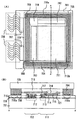
図1(A)に、本発明のEL表示装置の上面図を示す。画素基板701上に画素部711及びゲート信号線駆動回路702、ソース信号線駆動回路703が形成されている。この周りを囲んでシール材704が形成され、カバー材705が貼り付けられている。FPC基板706は、外部入力端子707によって画素基板701上に接続されている。配線708は、外部入力端子707において、FPC基板706からの信号を受け取り、ゲート信号線駆動回路702に伝達する、信号線や電源線等の複数の配線を示す。配線709は、外部入力端子707において、FPC基板706からの信号を受け取り、ソース信号線駆動回路703に伝達する、信号線や電源線等の複数の配線を示す。配線710(配線710a及び配線710b)は、外部入力端子707において、FPC基板706からの信号を受け取り、画素部711に伝達する、電源線等の複数の配線を示す。ここで、配線708〜710は、封止領域に形成されている。
【0044】
図1(B)は、図1(A)のA〜A'の部分を示した断面図である。
【0045】
なおここでは説明を簡単にするため、ゲート信号線駆動回路702を構成する素子としてTFT712、画素部711を構成する素子としてEL駆動用TFT713のみを示す。EL駆動用TFT713のソース領域もしくはドレイン領域のどちらか一方が、EL素子721の画素電極714と接続され、EL素子721に入力される電流を制御する。ここで、716は層間絶縁膜、715はEL層、717は絶縁膜、718は対向電極、719は充填材、720はゲート絶縁膜である。なお、ここでは、層間絶縁膜716は無機物質によって形成されているものとする。
【0046】
TFT712及びEL駆動用TFT713のソース配線及びドレイン配線を構成する物質と同様の物質を用い、配線708、配線710a及び配線710bが形成されている。
【0047】
なお、配線708〜710のうち配線709については、配線708、配線710a及び配線710bと同様に形成されるので、説明を省略する。
【0048】
ここで、シール材704として紫外線により硬化する材料を用いる場合が多い。また、カバー材705として遮光性を有する材料を用いる場合が多い。そのため、カバー材705側から紫外線照射してもシール材704を露光することができず、シール材704を硬化させることができない。そこで、画素基板701側から、配線708、配線710a及び配線710bを介して紫外線照射し、シール材704を露光させる必要がある。
【0049】
ここで、配線708、配線710a及び配線710bのうち、ビデオ信号線やパルス線などは、比較的幅の狭い配線を用いる。一方、画素部の電源供給線へ電流を供給する電源線や、ソース信号線駆動回路やゲート信号線駆動回路の電源線等に入力される電圧は、ビデオ信号線やパルス線に入力される電圧と比べて大きい。そのため、これらの電源線は、ビデオ信号線やパルス線と比較して幅の広い配線を使用する必要がある。
【0050】
しかし、幅の広い配線を用いると、配線を介して紫外線を照射した場合に配線の陰になったシール材部分に、十分に紫外線が照射されない。すると、シール材が十分に硬化しない可能性がある。
【0051】
そこで、本発明では、次のような配線の形状を考えた。その模式図を図3(A)に示す。なお、図3(A)は、図1の封止領域の一部666の拡大図に相当する。
【0052】
図3(A)では、配線(第1の配線)710bのうち、ある1本の電源線777に注目している。電源線777は、配線(第2の配線)A1〜A6を並列に接続することにより形成されている。ここで、この様な形状の配線777を介してシール材704に紫外線を照射する場合の説明をする。
【0053】
なお、ここでは、1本の電源線777を6本の配線A1〜A6を並列に接続することによって構成しているが、本発明はこの構成に限定されない。一般に、1本の配線が、n(nは、2以上の自然数)本の配線(第2の配線)A1〜Anを並列に接続することによって構成されていてもよい。
【0054】
図3(B)は、図3(A)のA〜A'の断面図である。図3(B)において、図3(A)と同じ符号は同じ部分を示す。
【0055】
図3(B)において、画素基板側から紫外線を照射すると配線A1〜A6の上のシール材の部分660は陰になるが、配線の幅Lが十分に小さく、かつ配線の間隔Sが十分に大きいとき、照射された紫外線は陰660の部分にも回り込む。
なお、配線のすぐ上部600の部分は紫外線によって露光されないが、配線幅が大きい場合と比べて、この600の部分は十分に小さく、全体としてシール材を十分に露光することができる。
【0056】
具体的には、配線A1〜A6の幅Lが100μm〜200μmの値を取り、配線A1〜A6のそれぞれの配線間の間隔Sが50μm〜150μmの値をとり、L/Sが0.7〜1.5になるような形状の配線の場合、その配線を介して照射された紫外線は、配線上部のシール材を十分に露光し、シール材を十分に硬化することができる。
【0057】
更に好ましくは、配線A1〜A6の幅Lが150μm以下の値を取り、配線A1〜A6のそれぞれの配線間の間隔Sが、100μm以上の値をとり、L/Sが、1.5以下の値となるような形状の配線の場合、その配線上部のシール材を十分に硬化することができる。
【0058】
なお、図3では、配線710bのうち、ある1本の電源線777に注目したが、封止領域に形成された、その他の配線幅が問題となる配線においても、同様の形状とすることができる。
【0059】
この様に、封止領域に配線を形成することができる。これにより、画素部以外の領域の面積を少なくすることができ、表示装置を小型化することができる。
【0060】
【実施例】
以下に、本発明の実施例について説明する。
【0061】
(実施例1)
本実施例では、発明の実施の形態とは異なった構成のアクティブマトリクス型EL表示装置について図2を用いて説明する。なお、図1と同じ部分は、同じ符号を用いて表す。
【0062】
図2(A)に、本発明のEL表示装置の上面図を示す。画素基板701上に画素部711及びゲート信号線駆動回路702、ソース信号線駆動回路703が形成されている。この周りを囲んでシール材704が形成され、カバー材705が貼り付けられている。FPC基板706は、外部入力端子707によって画素基板701上に接続されている。配線708は、外部入力端子707において、FPC基板706からの信号を受け取り、ゲート信号線駆動回路702に伝達する、信号線や電源線等の複数の配線を示す。配線709は、外部入力端子707において、FPC基板706からの信号を受け取り、ソース信号線駆動回路703に伝達する、信号線や電源線等の複数の配線を示す。配線710a及び配線710bは、外部入力端子707において、FPC基板706からの信号を受け取り、画素部711に伝達する、電源線等の複数の配線を示す。ここで、配線708〜710は、封止領域に形成されている。
【0063】
図2(B)は、図2(A)のA〜A'の部分を示した断面図である。
【0064】
なおここでは、説明を簡単にするため、ゲート信号線駆動回路702を構成する素子としてTFT712、画素部711を構成する素子としてEL駆動用TFT713のみを示す。EL駆動用TFT713のソース領域もしくはドレイン領域のどちらか一方が、EL素子721の画素電極714と接続され、EL素子721に入力される電流を制御する。ここで、層間絶縁膜716、EL層715、絶縁膜717、対向電極718、充填材719、ゲート絶縁膜720である。なお、ここでは、層間絶縁膜716は有機物質によって形成されているものとする。
【0065】
TFT712及びEL駆動用TFT713のソース配線及びドレイン配線を構成する物質と同様の物質を用い、配線708、配線710a及び配線710bが形成されている。
【0066】
なお、配線708〜710のうち配線709については、配線708、配線710a及び配線710bと同様に形成されるので、説明を省略する。
【0067】
層間絶縁膜716として、有機物質が使用されているため、この有機物質上に直接、配線708、配線710a及び配線710bを形成すると密着性が悪い。
また、有機物質から配線708、配線710a及び配線710bを構成する材料に不純物が導入されて配線708、配線710a及び配線710bが劣化するなどの問題がある。そこで、有機物質で形成された層間絶縁膜716を除いて配線708、配線710a及び配線710bを形成する必要がある。
【0068】
なお、配線708、配線710a及び配線710bを形成する部分の層間絶縁膜716を取り除く工程は、TFT712や画素TFT713のソース配線及びドレイン配線を形成する際、それらのTFTのソース領域に達するコンタクトホールを形成する時に同時に行うことができる。
【0069】
また、シール材704として、紫外線により硬化する材料を用いる場合が多い。また、カバー材705として遮光性を有する材料を用いる場合が多い。そのため、カバー材側から紫外線照射してもシール材を硬化させることができない。そこで、画素基板701側から、配線708、配線710a及び配線710bを介して紫外線照射し、シール材704を硬化させる必要がある。しかし配線708、配線710a及び配線710bとして、幅の広い配線を用いると、配線の陰になったシール材704の部分は、十分に紫外線が照射されずシール材704が十分に硬化しない可能性がある。
【0070】
そこで、配線708、配線710a及び配線710bとして、1本の幅の広い配線を用いる代わりに、図3に示した様に、複数の配線を並列に接続したものを用いる。
【0071】
具体的には、複数の配線の幅Lが100μm〜200μmの値をとり、複数の配線の間隔Sが50μm〜150μmの値をとり、複数の配線の幅Lと複数の配線の間隔Sとの比L/Sが、0.7〜1.5になるような形状の配線を用いる。このような形状の配線の場合、その配線を介して照射された紫外線は、配線上部のシール材を十分に露光し、シール材を十分に硬化することができる。
【0072】
更に好ましくは、複数の配線の幅Lが150μm以下の値を取り、複数の配線の間隔Sが、100μm以上の値をとり、L/Sが、1.5以下の値となるような形状の配線の場合、その配線上部のシール材を十分に硬化することができる。
【0073】
この様に、封止領域に配線を形成することができる。これにより、画素部以外の領域の面積を少なくすることができ、表示装置を小型化することができる。
【0074】
(実施例2)
本実施例では、アクティブマトリクス型EL表示装置の画素部の電源供給線に電流を供給する電源線の配線例について説明する。
【0075】
ここで、再び図1(A)を参照する。EL素子721を駆動する電流は、配線710a及び配線710bの電源線を通って、画素部711の電源供給線に入力される。画素部711の電源供給線は、710a及び710bの電源線により、2箇所から電流が供給されている。
【0076】
一方、図4に示した従来のEL表示装置では、画素部402の電源供給線は、412aの電源線より、1箇所から電流が供給されている。本発明のアクティブマトリクス型EL表示装置において、画素部の2箇所から画素部に電流を供給している理由を説明する。
【0077】
1つのFPC基板が接続された外部入力端子が一箇所にあり、画素部の一方から、電流が供給される場合と、外部入力端子が二箇所に分割してあり、それぞれにFPC基板(第1のFPC基板及び第2のFPC基板)が接続され、画素部の2方向から電源供給線に電流が供給される場合の、電源線の配線例を図5に模式的に示す。電源線として、EL素子の陽極に接続する陽極線と、陰極に接続する陰極線を示す。図5(A)は、外部入力端子707が一箇所にある。一方、図5(B)では外部入力端子707を二箇所(基板の一端及び前記基板の一端とは異なる基板の一端近傍)に分割し、それぞれから、陽極線及び陽極線を画素部に配線している。
【0078】
図5(A)では、陽極線及び陰極線の入力口から離れた側の電源供給線では、R1の長さの分だけ配線抵抗が増加し、それによる電位降下のため、電源供給線よりEL素子に印加される電圧が低下し、画質の低下を招く。
【0079】
一方、図5(B)では、一方の陽極線及び陰極線の入力口1から離れた側に、もう一方の入力口2を設け、入力口1及び入力口2の両方から電源供給線に電流を供給する。これにより、配線抵抗による電圧の低下に由来する、画質の低下を軽減することができる。
【0080】
なお、図5(B)の様に外部入力端子を2箇所に設ける際、この2つの外部入力端子間の距離を、画素部の形成された基板の長辺の長さの1/2以上離すことで、配線抵抗による電圧の低下に由来する画質の低下を軽減する効果が高まる。
【0081】
なお、配線抵抗がそれ程問題とならない場合は、外部入力端子を1箇所に形成してもよい。
【0082】
なお、本実施例は、発明の実施の形態や実施例1と組み合わせて実行することが可能である。
【0083】
(実施例3)
本実施例では、封止領域部分に配線を形成する手法を用いた液晶表示装置について説明する。
【0084】
液晶表示装置の駆動方法としては、アクティブマトリクス型が挙げられる。
【0085】
まず、図10にアクティブマトリクス型液晶表示装置の画素部の構成を示す。
アクティブマトリクス型液晶表示装置では、各画素がそれぞれTFTを有している。ゲート信号線駆動回路からの選択信号が入力されるゲート信号線(G1〜Gy)は、各画素が有する画素TFT1002のゲート電極に接続されている。また、各画素の有する画素TFT1002のソース領域とドレイン領域は、一方がソース信号線駆動回路から信号が入力されるソース信号線(S1〜Sx)に、他方が、保持容量1001の一方の電極と、液晶1003を挟む2つの電極の一方と接続されている。
【0086】
ゲート信号線G1に信号が入力されるとゲート信号線G1に接続されたすべての画素TFT1002のゲート電極に信号が入力され、画素TFT1002は、オンになる。画素TFT1002がオンになった画素に、ソース信号線(S1〜Sx)から信号が入力されると、保持容量1001に電荷が保持され、この保持された電荷により液晶1003を挟んだ電極間に電圧が印加される。この印加電圧により、液晶分子の配向を制御し、透過光量を制御する。すべてのゲート信号線(G1〜Gy)に関してこの動作を繰り返し、画像の表示を行う。
【0087】
次に、アクティブマトリクス型液晶表示装置の液晶の封止について説明する。
【0088】
液晶表示装置では、液晶を挟んだ2つの電極間に電圧を印加することによって、液晶の配向を制御し、表示を行う。ここで、電極間に液晶を挟んだ状態を保持する為、それぞれに電極が形成された2つの絶縁基板を、それぞれの電極が向かい合う向きにシール材で接着し、その間に液晶を封入する必要がある。
【0089】
図6に、液晶表示装置の2つの基板を貼り合わせて、その間に液晶を封入したところの模式図を示す。
【0090】
図6(A)は、液晶表示装置の上面図である。シール材301としては、エポキシ系樹脂等が用いられる。配向膜(図示せず)を形成し、ラビング処理を施された基板31において、画素部302及びゲート信号線駆動回路303、ソース信号線駆動回路304を囲むようにシール材301を形成する。この際、後に液晶を注入する為の注入口として開口部(図示せず)をシール材301の一部に形成しておく。次にスペーサー(図示せず)を散布し、もう一方の基板32と貼り合わせる。
【0091】
スペーサ−の径によって、基板31と基板32との距離が定まったら、基板31もしくは基板32を介して、シール材301部分に紫外線を照射したり、熱を加えるなどして、シール材301を硬化させ、基板31と基板32とを密着させる。
【0092】
なお、熱を加えることによって、シール材301を硬化させ、基板31と基板32とを貼り合わせる手法では、加圧しながら熱処理する必要があり、基板31と基板32の熱膨張により、張り合わせの位置がずれる問題が深刻である。また、熱硬化には時間がかかるという問題もある。その為、熱硬化ではなく、紫外線照射により、シール材を硬化させる工程が多く使用される。
【0093】
その後、液晶注入口より液晶33を注入し、封止材(図示せず)により液晶注入口をふさいで液晶33が外部に流れ出てこないようにする。なお、この封止材としては、熱硬化の材料ではなく、紫外線により硬化する材料を用いる。これは、液晶33を注入した後に熱を加えた場合、液晶33が劣化するのを防ぐためである。
【0094】
シール材301や封止材には、イオンを含む湿気などの液晶を汚染する物質を、通過させないようにする働きもある。
【0095】
次に、ソース信号線駆動回路及びゲート信号線駆動回路のそれぞれに入力される信号を伝達する配線について説明する。
【0096】
外部からのビデオ信号などが、ゲート信号線駆動回路303及びソース信号線駆動回路304に入力され、画素部302に入力される信号が構成される。ここで、外部からゲート信号線駆動回路303及びソース信号線駆動回路304に入力される信号は、画素基板31上の外部入力端子309に貼り付けられた、FPC基板310より入力される。FPC基板310は、外部入力端子309において、異方性導電性膜(図示せず)によって画素基板上に形成された配線312と接続される。この配線312(312a、312b)は、シール材301の間を通ってゲート信号線駆動回路303及びソース信号線駆動回路304に接続されている。
【0097】
配線312aは、外部入力端子309において、FPC基板310からの信号を受け取り、ゲート信号線駆動回路303に伝達する配線である。配線312bは、外部入力端子309において、FPC基板310からの信号を受け取り、ソース信号線駆動回路304に伝達する配線である。ここで、配線312a及び配線312bは、画素基板31上のシール材301に覆われた部分(封止領域)に形成されている。
【0098】
図6(B)に図6(A)のB〜B'の断面図を示す。なお、図6(A)と同じ部分は、同じ符号で表す。
【0099】
ここでは、説明を簡単にするため、ゲート信号線駆動回路303を構成するTFT114及び画素部302を構成する画素TFT314のみを示す。画素部及び駆動回路を構成するTFTが形成された基板31を画素基板と呼ぶことにする。また、画素基板上に取り付けられた電極307を画素電極と呼ぶ。もう一方の基板32は、対向基板と呼ぶことにする。また、対向基板側に取り付けられた電極308を対向電極と呼ぶ。この画素電極307や対向電極308に印加される電圧を制御して画像の表示を行う。
【0100】
ここで、306はTFT114及びTFT画素314のゲート絶縁膜である。
また、315は層間絶縁膜、112は遮光層である。なお、ここでは配向膜は図示していない。
【0101】
画素TFT314のソース領域もしくはドレイン領域のどちらか一方が、画素電極307と接続し、画素電極307に印加される電圧を制御している。なお、ここでは、層間絶縁膜315は無機物質によって形成されているものとする。
【0102】
ここで、TFT114や画素TFT314のソース配線及びドレイン配線を構成する物質と同様の物質を用い、配線312が形成されている。
【0103】
また、シール材301として紫外線により硬化する材料を用いたとする。対向基板32側から紫外線照射しても、遮光層112があるためシール材301を硬化させることができない。そこで、画素基板31側から、配線312aを介して紫外線照射し、シール材301を硬化させる必要がある。しかし、配線312aとして幅の広い配線を用いると、配線の陰になったシール材704の部分は、十分に紫外線が照射されずシール材704が十分に硬化しない可能性がある。
【0104】
そこで、配線312aとして、1本の幅の広い配線を用いる代わりに、図3に示した様に、複数の配線を並列に接続したものを用いる。
【0105】
具体的には、複数の配線の幅Lが100μm〜200μmの値をとり、複数の配線の間隔Sが50μm〜150μmの値をとり、複数の配線の幅Lと複数の配線の間隔Sとの比L/Sが、0.7〜1.5になるような形状の配線を用いる。このような形状の配線の場合、その配線を介して照射された紫外線は、配線上部のシール材を十分に露光し、シール材を十分に硬化することができる。
【0106】
更に好ましくは、複数の配線の幅Lが150μm以下の値を取り、複数の配線の間隔Sが、100μm以上の値をとり、L/Sが、1.5以下の値となるような形状の配線の場合、その配線上部のシール材を十分に硬化することができる。
【0107】
なお、遮光層112が画素基板31側に取り付けられている場合には,シール材301を硬化させるために対向基板32側から紫外線を照射する必要がある。この時は、配線312aは、照射される紫外線を遮ることは無いので、幅の広い形状のものを用いても問題ない。
【0108】
この様に、封止領域に配線を形成することができる。これにより、画素部以外の領域の面積を少なくすることができ、表示装置を小型化することができる。
【0109】
(実施例4)
本実施例では、実施例3に述べた構造とは異なる構造の表示装置について、図7を用いて説明する。なお、図7において、図6と同じ部分は同じ符号を用いて表す。
【0110】
図7(A)は、本発明の液晶表示装置の上面図である。画素基板31上に画素部302及びゲート信号線駆動回路303、ソース信号線駆動回路304が形成されている。この周りを囲んでシール材301が形成され、対向基板32が貼り付けられ、間に液晶33が封入されている。FPC基板310は、外部入力端子309によって画素基板31上に接続されている。配線312aは、外部入力端子309において、FPC基板310からの信号を受け取り、ゲート信号線駆動回路303に伝達する配線である。配線312bは、外部入力端子309において、FPC基板310からの信号を受け取り、ソース信号線駆動回路304に伝達する配線である。ここで、配線312a及び配線312bは、封止領域に形成されている。
【0111】
図7(B)は、図7(A)のB〜B'の部分を示した断面図である。ここで、図7(A)と同じ符号は同じ部分を表す。
【0112】
ここでは説明を簡単にするため、ゲート信号線駆動回路303を構成する素子としてTFT114のみを示す。また、画素部302を構成する素子として画素TFT314のみを示す。画素TFT314のソース領域もしくはドレイン領域のどちらか一方が、画素電極307と接続し、画素電極307に印加される電圧を制御している。
【0113】
TFT114や画素TFT314のソース配線及びドレイン配線を構成する物質と同様の物質を用い、配線312が形成されている。なお、ここでは、層間絶縁膜315は有機物質によって形成されているものとする。
【0114】
層間絶縁膜315として、有機物質が使用されているため、この有機物質上に直接、配線312を形成すると密着性が悪い。また、有機物質から配線312を構成する材料に不純物が導入されて配線312が劣化するなどの問題がある。そこで、有機物質で形成された層間絶縁膜315を除いて配線312を形成する必要がある。
【0115】
なお、配線312aを形成する部分の層間絶縁膜315を取り除く工程は、TFT114や画素TFT314のソース配線及びドレイン配線を形成する際、それらのソース領域及びドレイン領域に達するコンタクトホールを形成する時に同時に行うことができる。
【0116】
また、シール材301として紫外線により硬化する材料を用いたとする。対向基板32側から紫外線照射しても、遮光層112があるためシール材301を硬化させることができない。そこで、画素基板31側から、配線312aを介して紫外線照射し、シール材301を硬化させる必要がある。しかし、配線312aとして幅の広い配線を用いると、配線の陰になったシール材704の部分は、十分に紫外線が照射されずシール材704が十分に硬化しない可能性がある。
【0117】
そこで配線312aとして、1本の幅の広い配線を用いる代わりに、図3に示した様に、複数の配線を並列に接続したものを用いる。
【0118】
具体的には、複数の配線の幅Lが100μm〜200μmの値をとり、複数の配線の間隔Sが50μm〜150μmの値をとり、複数の配線の幅Lと複数の配線の間隔Sとの比L/Sが、0.7〜1.5になるような形状の配線を用いる。このような形状の配線の場合、その配線を介して照射された紫外線は、配線上部のシール材を十分に露光し、シール材を十分に硬化することができる。
【0119】
更に好ましくは、複数の配線の幅Lが150μm以下の値を取り、複数の配線の間隔Sが、100μm以上の値をとり、L/Sが、1.5以下の値となるような形状の配線の場合、その配線上部のシール材を十分に硬化することができる。
【0120】
なお、遮光層112が画素基板31側に取り付けられている場合には,シール材301を硬化させるために対向基板32側から紫外線を照射する事となる。この時は、配線312aは、照射される紫外線を遮ることは無いので、幅の広い形状のものを用いても問題ない。
【0121】
この様に、封止領域に配線を形成することができる。これにより、画素部以外の領域の面積を少なくすることができ、表示装置を小型化することができる。
【0122】
(実施例5)
本実施例では、本発明を用いて形成された表示装置を表示媒体として組み込んだ電子機器について説明する。
【0123】
その様な電子機器としては、ビデオカメラ、デジタルカメラ、ヘッドマウントディスプレイ(ゴーグル型ディスプレイ)、ゲーム機、カーナビゲーション、パーソナルコンピュータ、携帯情報端末(モバイルコンピュータ、携帯電話または電子書籍等)などが挙げられる。それらの一例を図8に示す。
【0124】
図8(A)はパーソナルコンピュータであり、本体2001、筐体2002、表示部2003、キーボード2004等を含む。本発明の表示装置はパーソナルコンピュータの表示部2003に用いることができる。
【0125】
図8(B)はビデオカメラであり、本体2101、表示部2102、音声入力部2103、操作スイッチ2104、バッテリー2105、受像部2106等を含む。本発明の表示装置はビデオカメラの表示部2102に用いることができる。
【0126】
図8(C)は頭部取り付け型の表示装置の一部(右片側)であり、本体2301、信号ケーブル2302、頭部固定バンド2303、表示モニタ2304、光学系2305、表示部2306等を含む。本発明の表示装置は頭部取り付け型の表示装置の表示部2306に用いることができる。
【0127】
図8(D)は記録媒体を備えた画像再生装置(具体的にはDVD再生装置)であり、本体2401、記録媒体(CD、LDまたはDVD等)2402、操作スイッチ2403、表示部(a)2404、表示部(b)2405等を含む。表示部(a)は主として画像情報を表示し、表示部(b)は主として文字情報を表示するが、本発明の表示装置は記録媒体を備えた画像再生装置の表示部(a)2404、表示部(b)2405に用いることができる。なお、記録媒体を備えた画像再生装置としては、CD再生装置、ゲーム機器などに本発明を用いることができる。
【0128】
図8(E)は携帯型(モバイル)コンピュータであり、本体2501、カメラ部2502、受像部2503、操作スイッチ2504、表示部2505等を含む。本発明の表示装置2505は携帯型(モバイル)コンピュータの表示部2505に用いることができる。
【0129】
以上の様に、本発明の適用範囲は極めて広く、あらゆる分野の電子機器に適用することが可能である。また、本実施例の電子機器は実施例1〜4のどのような組み合わせからなる構成を用いても実現することができる。
【0130】
【発明の効果】
EL表示装置や液晶表示装置などの表示装置において、駆動回路周辺の配線が占める部分や、シール材が形成された部分等、画像を表示しない部分の占める面積が大きく、表示装置の小型化において問題となっていた。
【0131】
しかし、本発明は、上記構成によって、駆動回路周辺の配線をシール材の部分にも形成することができる。これにより、小型の表示装置を提供することができる。
【図面の簡単な説明】
【図1】 本発明のEL表示装置の上面図及び断面図。
【図2】 本発明のEL表示装置の上面図及び断面図。
【図3】 本発明の表示装置の配線の形状を示す図。
【図4】 従来のEL表示装置の上面図及び断面図。
【図5】 本発明の表示装置の電源線の配線を示す図。
【図6】 本発明の液晶表示装置の上面図及び断面図。
【図7】 本発明の液晶表示装置の上面図及び断面図。
【図8】 本発明の表示装置を用いた電子機器の図。
【図9】 EL表示装置の画素部の構成を示す図。
【図10】 液晶表示装置の画素部の構成を示す図。[0001]
BACKGROUND OF THE INVENTION
The present invention relates to a display device having a sealing structure. In particular, the present invention relates to an active matrix display device using a semiconductor element (an element using a semiconductor thin film). Further, the present invention relates to an electronic device using an active matrix display device for a display portion.
[0002]
[Prior art]
In recent years, an electro-optical device such as an EL display device having an EL element has attracted attention as a flat display.
[0003]
An EL element has a structure in which an EL layer is sandwiched between a pair of electrodes (anode and cathode), and the EL layer usually has a laminated structure. A typical example is a “hole transport layer / light emitting layer / electron transport layer” stacked structure proposed by Tang et al. Of Kodak Eastman Company. This structure has very high luminous efficiency, and most EL display devices that are currently under research and development employ this structure.
[0004]
In addition, the hole injection layer / hole transport layer / light emitting layer / electron transport layer, or hole injection layer / hole transport layer / light emitting layer / electron transport layer / electron injection layer are laminated in this order on the anode. Structure may be sufficient. You may dope a fluorescent pigment | dye etc. with respect to a light emitting layer.
[0005]
In this specification, all layers provided between a cathode and an anode are collectively referred to as an EL layer. Therefore, the above-described hole injection layer, hole transport layer, light emitting layer, electron transport layer, electron injection layer, and the like are all included in the EL layer.
[0006]
Then, a predetermined voltage is applied to the EL layer having the above structure from the pair of electrodes, whereby recombination of carriers occurs in the light emitting layer to emit light. Note that light emission of an EL element in this specification is referred to as driving of the EL element. In this specification, a light-emitting element formed using an anode, an EL layer, and a cathode is referred to as an EL element.
[0007]
Note that in this specification, an EL element refers to both an element that uses light emission (fluorescence) from a singlet exciton and an element that uses light emission (phosphorescence) from a triplet exciton.
[0008]
As a structure of the EL display device, an active matrix type can be given.
[0009]
FIG. 9 illustrates an example of a structure of a pixel portion of an active matrix EL display device. In an active matrix EL display device, each pixel has a thin film transistor (hereinafter referred to as TFT). Gate signal lines (G1 to Gy) for inputting selection signals from the gate signal line driving circuit are connected to the gate electrode of the switching TFT 901 included in each pixel. One of the source region and the drain region of the switching TFT 901 included in each pixel is a source signal line (S1 to Sx) for inputting a signal from the source signal line driver circuit, and the other is a gate electrode of the EL driving TFT 902 and each It is connected to one electrode of a capacitor 903 included in the pixel. The other electrode of the capacitor 903 is connected to the power supply line (V1 to Vx). One of a source region and a drain region of the EL driving TFT 902 included in each pixel is connected to a power supply line (V1 to Vx), and the other is connected to an EL element 904 included in each pixel.
[0010]
When the gate signal line G1 is selected by the gate signal line driving circuit and a signal is input, the switching TFT 901 connected to the gate signal line G1 is turned on. Here, when a signal is input to the source signal lines S1 to Sx from the source signal line driving circuit, the EL driving TFT 902 is turned on in the pixel to which the signal is input, and the EL is supplied from the power supply line (V1 to Vx). A current flows through the element 904, and the EL element 904 emits light. This operation is repeated for all the gate signal lines G1 to Gy to display an image.
[0011]
The EL element 904 includes an anode, a cathode, and an EL layer provided between the anode and the cathode. In the case where the anode of the EL element 904 is connected to the source region or the drain region of the EL driving TFT 902, the anode of the EL element 904 is a pixel electrode and the cathode is a counter electrode. On the other hand, in the case where the cathode of the EL element 904 is connected to the source region or the drain region of the EL driving TFT 902, the cathode of the EL element 904 is a pixel electrode and the anode is a counter electrode.
[0012]
Note that in this specification, the potential of the counter electrode is referred to as a counter potential. A power source that applies a counter potential to the counter electrode is referred to as a counter power source. The potential difference between the potential of the pixel electrode and the potential of the counter electrode is an EL drive voltage, and this EL drive voltage is applied to the EL layer.
[0013]
Here, there is a problem that the organic EL layer is deteriorated by moisture or oxygen. Therefore, after forming the EL layer, it is generally sealed with an ultraviolet curable resin in a nitrogen atmosphere without being exposed to the air. FIG. 4 shows an example of sealing an EL display device.
[0014]
FIG. 4A shows a top view of the EL display device. The
[0015]
FIG. 4B is a cross-sectional view taken along a line AA ′ in FIG.
[0016]
Note that only the
[0017]
Here, 406 is a gate insulating film of the
[0018]
Note that signals input to the
[0019]
[Problems to be solved by the invention]
In an EL display device, in order to prevent deterioration of an EL element, it is necessary to seal the EL element by bonding a pixel substrate and a cover material using a sealing material.
[0020]
Here, unlike the pixel portion, the seal material portion and each drive circuit portion are portions that do not display an image. In the conventional display device, the proportion of the portion that does not display the image is large with respect to the display screen, which is a problem in miniaturizing the display device.
[0021]
Thus, an object is to reduce the area of a portion other than the pixel portion in the display device.
[0022]
[Means for Solving the Problems]
Wiring is formed on the portion of the pixel substrate covered with the sealing material. Note that the line width of the wiring is set so that when the sealing material is irradiated with ultraviolet rays through the wiring, the sealing material on the wiring is sufficiently exposed to the ultraviolet rays.
[0023]
Accordingly, the area occupied by the wiring and the seal material around the pixel portion and the drive circuit portion in the display device can be reduced, and the display device can be downsized.
[0024]
The configuration of the present invention is shown below.
[0025]
According to the present invention,
A substrate, a cover material, and a sealing material;
A plurality of pixels on the substrate; and a driving circuit for inputting signals to the plurality of pixels;
Each of the plurality of pixels has an EL element,
The cover material has a light shielding property,
The sealing material has a material that is cured by ultraviolet rays,
The sealing material is disposed on the substrate so as to surround the plurality of pixels and the driving circuit, the cover material and the substrate are brought into close contact with the sealing material, and the EL element is sealed. In the display device,
A first wiring is formed between the sealing material and the substrate,
The display device is characterized in that the first wiring has a plurality of second wirings connected in parallel.
[0026]
A portion of the substrate that is in contact with the sealing material may be formed of an inorganic substance.
[0027]
According to the present invention,
A first substrate, a second substrate, and a sealing material;
A plurality of pixels on the first substrate; and a driving circuit for inputting signals to the plurality of pixels;
The second substrate has a light shielding property,
The sealing material has a material that is cured by ultraviolet rays,
A sealing material is disposed on the first substrate so as to surround the plurality of pixels and the driving circuit, and the second substrate and the first substrate are brought into close contact with each other with the sealing material interposed therebetween. In a display device in which liquid crystal is sealed in a region surrounded by the first substrate, the second substrate, and the sealing material,
A first wiring is formed between the sealing material and the first substrate;
The display device is characterized in that the first wiring has a plurality of second wirings connected in parallel.
[0028]
A portion of the first substrate that is in contact with the sealing material may be formed of an inorganic substance.
[0029]
A ratio L / S of the width L of the plurality of second wirings connected in parallel to the interval S between the plurality of second wirings connected in parallel takes a value of 0.7 to 1.5. It may be a display device characterized by this.
[0030]
The width L of the plurality of second wirings connected in parallel takes a value of 100 μm to 200 μm,
The interval S between the plurality of second wirings connected in parallel may take a value of 50 μm to 150 μm.
[0031]
The display device may be characterized in that the wiring is formed of the same material as that of the source wiring and the drain wiring of the TFTs included in the plurality of pixels and the driving circuit.
[0032]
According to the present invention,
A plurality of pixels and a plurality of external input terminals on the substrate;
In the display device including the EL element, the plurality of pixels may include:
A display device is provided in which an anode line for supplying a current to the EL element is connected to the plurality of external input terminals.
[0033]
According to the present invention,
A plurality of pixels and a plurality of external input terminals on the substrate;
In the display device including the EL element, the plurality of pixels may include:
A display device is provided in which a cathode line for drawing current from the EL element is connected to the plurality of external input terminals.
[0034]
Among the plurality of external input terminals, at least one external input terminal is in the vicinity of one end of the substrate, and the other external input terminal is in the vicinity of one end of the substrate, which is different from one end of the substrate. It may be a display device characterized by.
[0035]
A display device may be characterized in that at least one of the plurality of external input terminals is connected to a first FPC board and the other is connected to a second FPC board.
[0036]
The display device may be characterized in that the distance between the plurality of external input terminals is at least half the length of the long side of the substrate.
[0037]
According to the present invention,
A display device comprising a substrate, a first wiring and a plurality of pixels formed on the substrate, a light-shielding cover material, and a sealing material,
The plurality of pixels formed on the substrate are sealed by the sealing material and the cover material,
The first wiring is covered with the sealing material;
The sealing material has a material that is cured by ultraviolet rays,
The display device is characterized in that the first wiring has a plurality of second wirings connected in parallel.
[0038]
According to the present invention,
A display device comprising a substrate, a first wiring and a plurality of pixels formed on the substrate, a light-shielding cover material, and a sealing material,
The plurality of pixels formed on the substrate are sealed by the sealing material and the cover material,
Each of the plurality of pixels has an EL element,
The first wiring is covered with the sealing material;
The sealing material has a material that is cured by ultraviolet rays,
The display device is characterized in that the first wiring has a plurality of second wirings connected in parallel.
[0039]
According to the present invention,
A display device comprising a substrate, a first wiring and a plurality of pixels formed on the substrate, a light-shielding cover material, a sealing material, and a liquid crystal,
The plurality of pixels formed on the substrate and the liquid crystal are sealed by the sealing material and the cover material,
The first wiring is covered with the sealing material;
The sealing material has a material that is cured by ultraviolet rays,
The display device is characterized in that the first wiring has a plurality of second wirings connected in parallel.
[0040]
A video camera, an image reproducing device, a head mounted display, a mobile phone, or a portable information terminal using the display device may be used.
[0041]
DETAILED DESCRIPTION OF THE INVENTION
An embodiment of the present invention will be described with reference to FIG.
[0042]
An EL display device in which wiring is formed in a portion covered with a sealing material on a pixel substrate will be described. In this specification, a portion covered with a sealant on the pixel substrate is referred to as a sealing region.
[0043]
FIG. 1A shows a top view of an EL display device of the present invention. A
[0044]
FIG. 1B is a cross-sectional view showing portions A to A ′ of FIG.
[0045]
Note that here, for simplicity of explanation, only the
[0046]
A
[0047]
Note that the
[0048]
Here, a material that is cured by ultraviolet rays is often used as the sealing
[0049]
Here, among the
[0050]
However, when a wide wiring is used, when the ultraviolet ray is irradiated through the wiring, the ultraviolet ray is not sufficiently irradiated to the sealing material portion that is behind the wiring. Then, the sealing material may not be cured sufficiently.
[0051]
Therefore, in the present invention, the following wiring shapes are considered. A schematic diagram thereof is shown in FIG. Note that FIG. 3A corresponds to an enlarged view of a
[0052]
In FIG. 3A, attention is paid to one
[0053]
Here, one
[0054]
FIG. 3B is a cross-sectional view taken along a line AA ′ in FIG. 3B, the same reference numerals as those in FIG. 3A denote the same parts.
[0055]
In FIG. 3B, when ultraviolet rays are irradiated from the pixel substrate side, the
In addition, although the part of 600 immediately above wiring is not exposed by an ultraviolet-ray, compared with the case where wiring width is large, this 600 part is small enough and can fully expose a sealing material as a whole.
[0056]
Specifically, the width L of the wirings A1 to A6 takes a value of 100 μm to 200 μm, the spacing S between the wirings A1 to A6 takes a value of 50 μm to 150 μm, and L / S is 0.7 to In the case of a wiring having a shape of 1.5, the ultraviolet light irradiated through the wiring can sufficiently expose the sealing material on the wiring and sufficiently cure the sealing material.
[0057]
More preferably, the width L of the wirings A1 to A6 takes a value of 150 μm or less, the interval S between the wirings A1 to A6 takes a value of 100 μm or more, and L / S is 1.5 or less. In the case of a wiring having such a shape, the sealing material on the upper part of the wiring can be sufficiently cured.
[0058]
In FIG. 3, attention is paid to one
[0059]
In this manner, wiring can be formed in the sealing region. Accordingly, the area of the region other than the pixel portion can be reduced, and the display device can be reduced in size.
[0060]
【Example】
Examples of the present invention will be described below.
[0061]
Example 1
In this embodiment, an active matrix EL display device having a structure different from that of the embodiment mode of the invention will be described with reference to FIG. The same parts as those in FIG. 1 are denoted by the same reference numerals.
[0062]
FIG. 2A shows a top view of the EL display device of the present invention. A
[0063]
FIG. 2B is a cross-sectional view showing portions A to A ′ of FIG.
[0064]
Note that here, for simplicity of description, only the
[0065]
A
[0066]
Note that the
[0067]
Since an organic material is used as the
In addition, there is a problem that impurities are introduced into a material forming the
[0068]
Note that in the step of removing the
[0069]
In many cases, a material that is cured by ultraviolet rays is used as the
[0070]
Therefore, as the
[0071]
Specifically, the width L of the plurality of wirings takes a value of 100 μm to 200 μm, the spacing S of the plurality of wirings takes a value of 50 μm to 150 μm, and the width L of the plurality of wirings and the spacing S of the plurality of wirings A wiring having a shape such that the ratio L / S is 0.7 to 1.5 is used. In the case of the wiring having such a shape, the ultraviolet rays irradiated through the wiring can sufficiently expose the sealing material on the upper part of the wiring and sufficiently cure the sealing material.
[0072]
More preferably, the width L of the plurality of wirings has a value of 150 μm or less, the interval S between the plurality of wirings has a value of 100 μm or more, and L / S has a value of 1.5 or less. In the case of wiring, the sealing material on the upper part of the wiring can be sufficiently cured.
[0073]
In this manner, wiring can be formed in the sealing region. Accordingly, the area of the region other than the pixel portion can be reduced, and the display device can be reduced in size.
[0074]
(Example 2)
In this embodiment, a wiring example of a power supply line for supplying current to a power supply line of a pixel portion of an active matrix EL display device will be described.
[0075]
Here, reference is again made to FIG. A current for driving the
[0076]
On the other hand, in the conventional EL display device shown in FIG. 4, the power supply line of the
[0077]
An external input terminal to which one FPC board is connected is provided at one place, and a current is supplied from one of the pixel portions, and an external input terminal is divided into two places. FIG. 5 schematically shows an example of wiring of power supply lines when a current is supplied to the power supply lines from two directions of the pixel portion. As power supply lines, an anode line connected to the anode of the EL element and a cathode line connected to the cathode are shown. In FIG. 5A, the
[0078]
In FIG. 5A, in the power supply line on the side away from the input port of the anode line and the cathode line, the wiring resistance increases by the length of R1, and the potential drop due thereto causes the EL element to exceed the power supply line. The voltage applied to the lowering causes a reduction in image quality.
[0079]
On the other hand, in FIG. 5 (B), the other input port 2 is provided on the side away from the
[0080]
Note that when two external input terminals are provided as shown in FIG. 5B, the distance between the two external input terminals is set to be 1/2 or more of the length of the long side of the substrate on which the pixel portion is formed. As a result, the effect of reducing the deterioration in image quality due to the decrease in voltage due to wiring resistance is enhanced.
[0081]
In the case where the wiring resistance does not matter so much, the external input terminal may be formed at one place.
[0082]
Note that this example can be implemented in combination with the embodiment of the invention or Example 1.
[0083]
(Example 3)
In this embodiment, a liquid crystal display device using a method of forming wiring in a sealing region portion will be described.
[0084]
As a driving method of the liquid crystal display device, an active matrix type can be given.
[0085]
First, FIG. 10 shows a structure of a pixel portion of an active matrix liquid crystal display device.
In the active matrix liquid crystal display device, each pixel has a TFT. Gate signal lines (G1 to Gy) to which a selection signal from the gate signal line driver circuit is input are connected to the gate electrode of the pixel TFT 1002 included in each pixel. One of a source region and a drain region of the pixel TFT 1002 included in each pixel is a source signal line (S1 to Sx) to which a signal is input from the source signal line driver circuit, and the other is an electrode of the storage capacitor 1001. The liquid crystal 1003 is connected to one of the two electrodes.
[0086]
When a signal is input to the gate signal line G1, a signal is input to the gate electrodes of all the pixel TFTs 1002 connected to the gate signal line G1, and the pixel TFT 1002 is turned on. When a signal is input from the source signal line (S1 to Sx) to the pixel in which the pixel TFT 1002 is turned on, the charge is held in the holding capacitor 1001, and a voltage is applied between the electrodes sandwiching the liquid crystal 1003 by the held charge. Is applied. By this applied voltage, the orientation of liquid crystal molecules is controlled, and the amount of transmitted light is controlled. This operation is repeated for all the gate signal lines (G1 to Gy) to display an image.
[0087]
Next, sealing of the liquid crystal of the active matrix liquid crystal display device will be described.
[0088]
In a liquid crystal display device, a voltage is applied between two electrodes sandwiching a liquid crystal, thereby controlling the alignment of the liquid crystal and performing display. Here, in order to maintain a state in which the liquid crystal is sandwiched between the electrodes, it is necessary to bond two insulating substrates each having an electrode formed thereon with a sealing material in a direction in which the electrodes face each other and enclose the liquid crystal therebetween. is there.
[0089]
FIG. 6 shows a schematic view of two substrates of a liquid crystal display device bonded together and liquid crystal sealed between them.
[0090]
FIG. 6A is a top view of the liquid crystal display device. As the sealing
[0091]
When the distance between the
[0092]
Note that in the method in which the sealing
[0093]
Thereafter, the
[0094]
The sealing
[0095]
Next, wirings for transmitting signals input to the source signal line driver circuit and the gate signal line driver circuit will be described.
[0096]
An external video signal or the like is input to the gate signal
[0097]
The
[0098]
FIG. 6B is a cross-sectional view taken along the line B-B ′ in FIG. Note that the same portions as those in FIG. 6A are denoted by the same reference numerals.
[0099]
Here, for simplification of description, only the
[0100]
Here,
[0101]
Either the source region or the drain region of the
[0102]
Here, the wiring 312 is formed using the same material as that constituting the source wiring and the drain wiring of the
[0103]
Further, it is assumed that a material curable by ultraviolet rays is used as the sealing
[0104]
Therefore, as the
[0105]
Specifically, the width L of the plurality of wirings takes a value of 100 μm to 200 μm, the spacing S of the plurality of wirings takes a value of 50 μm to 150 μm, and the width L of the plurality of wirings and the spacing S of the plurality of wirings A wiring having a shape such that the ratio L / S is 0.7 to 1.5 is used. In the case of the wiring having such a shape, the ultraviolet rays irradiated through the wiring can sufficiently expose the sealing material on the upper part of the wiring and sufficiently cure the sealing material.
[0106]
More preferably, the width L of the plurality of wirings has a value of 150 μm or less, the interval S between the plurality of wirings has a value of 100 μm or more, and L / S has a value of 1.5 or less. In the case of wiring, the sealing material on the upper part of the wiring can be sufficiently cured.
[0107]
When the
[0108]
In this manner, wiring can be formed in the sealing region. Accordingly, the area of the region other than the pixel portion can be reduced, and the display device can be reduced in size.
[0109]
Example 4
In this embodiment, a display device having a structure different from that described in Embodiment 3 will be described with reference to FIGS. In FIG. 7, the same parts as those in FIG. 6 are denoted by the same reference numerals.
[0110]
FIG. 7A is a top view of the liquid crystal display device of the present invention. A
[0111]
FIG. 7B is a cross-sectional view showing portions B to B ′ of FIG. Here, the same reference numerals as those in FIG. 7A denote the same parts.
[0112]
Here, for simplicity of explanation, only the
[0113]
The wiring 312 is formed using the same material as that constituting the source wiring and the drain wiring of the
[0114]
Since an organic material is used as the
[0115]
Note that the step of removing the
[0116]
Further, it is assumed that a material curable by ultraviolet rays is used as the sealing
[0117]
Therefore, instead of using one wide wiring as the
[0118]
Specifically, the width L of the plurality of wirings takes a value of 100 μm to 200 μm, the spacing S of the plurality of wirings takes a value of 50 μm to 150 μm, and the width L of the plurality of wirings and the spacing S of the plurality of wirings A wiring having a shape such that the ratio L / S is 0.7 to 1.5 is used. In the case of the wiring having such a shape, the ultraviolet rays irradiated through the wiring can sufficiently expose the sealing material on the upper part of the wiring and sufficiently cure the sealing material.
[0119]
More preferably, the width L of the plurality of wirings has a value of 150 μm or less, the interval S between the plurality of wirings has a value of 100 μm or more, and L / S has a value of 1.5 or less. In the case of wiring, the sealing material on the upper part of the wiring can be sufficiently cured.
[0120]
When the
[0121]
In this manner, wiring can be formed in the sealing region. Accordingly, the area of the region other than the pixel portion can be reduced, and the display device can be reduced in size.
[0122]
(Example 5)
In this embodiment, an electronic device in which a display device formed using the present invention is incorporated as a display medium will be described.
[0123]
Examples of such electronic devices include video cameras, digital cameras, head mounted displays (goggles type displays), game machines, car navigation systems, personal computers, personal digital assistants (mobile computers, mobile phones, electronic books, etc.), and the like. . An example of them is shown in FIG.
[0124]
FIG. 8A illustrates a personal computer, which includes a main body 2001, a housing 2002, a display portion 2003, a
[0125]
FIG. 8B shows a video camera, which includes a main body 2101, a display portion 2102, an
[0126]
FIG. 8C shows a part of the head-mounted display device (on the right side), which includes a main body 2301, a signal cable 2302, a
[0127]
FIG. 8D shows an image reproducing device (specifically, a DVD reproducing device) provided with a recording medium, which includes a main body 2401, a recording medium (CD, LD, DVD, etc.) 2402, an
[0128]
FIG. 8E illustrates a portable (mobile) computer, which includes a main body 2501, a camera portion 2502, an
[0129]
As described above, the application range of the present invention is extremely wide and can be applied to electronic devices in various fields. Moreover, the electronic device of a present Example is realizable even if it uses the structure which consists of what combination of Examples 1-4.
[0130]
【The invention's effect】
In a display device such as an EL display device or a liquid crystal display device, the area occupied by a portion that does not display an image, such as a portion occupied by wiring around a drive circuit or a portion where a seal material is formed, is a problem in downsizing the display device. It was.
[0131]
However, according to the present invention, the wiring around the drive circuit can be formed also in the seal material portion by the above configuration. Thereby, a small display device can be provided.
[Brief description of the drawings]
1A and 1B are a top view and a cross-sectional view of an EL display device of the present invention.
2A and 2B are a top view and a cross-sectional view of an EL display device of the present invention.
FIG. 3 is a diagram showing a wiring shape of a display device of the present invention.
4A and 4B are a top view and a cross-sectional view of a conventional EL display device.
FIG. 5 is a diagram showing wiring of power supply lines of a display device of the present invention.
6A and 6B are a top view and a cross-sectional view of a liquid crystal display device of the present invention.
7A and 7B are a top view and a cross-sectional view of a liquid crystal display device of the present invention.
FIG. 8 is a diagram of an electronic device using the display device of the invention.
FIG 9 illustrates a structure of a pixel portion of an EL display device.
FIG 10 illustrates a structure of a pixel portion of a liquid crystal display device.
Claims (17)
遮光性を有する第2の基板と、
紫外線により硬化する材料を用いて形成され、前記第1の基板と前記第2の基板とを貼り合わせるシール材とを有し、
前記シール材と前記第1の基板との間に第1の配線が形成され、
前記第1の配線は、前記シール材の少なくとも一辺に沿って重なって設けられ、前記第1の配線は、前記シール材の一辺と重なる領域においてそれぞれが並列に接続された複数の第2の配線を有することを特徴とする表示装置。A first substrate provided with a plurality of pixels;
A second substrate having light shielding properties;
A sealant that is formed using a material that is cured by ultraviolet rays, and that bonds the first substrate and the second substrate;
A first wiring is formed between the sealing material and the first substrate;
The first wiring is provided so as to overlap along at least one side of the sealing material, and the first wiring is a plurality of second wirings each connected in parallel in a region overlapping with one side of the sealing material. A display device comprising:
第2の基板と、
紫外線により硬化する材料を用いて形成され、前記第1の基板と前記第2の基板とを貼り合わせるシール材と、
前記第2の基板と、シール材との間に設けられた遮光層とを有し、
前記シール材と前記第1の基板との間に第1の配線が形成され、
前記第1の配線は、前記シール材の少なくとも一辺に沿って重なって設けられ、前記第1の配線は、前記シール材の一辺と重なる領域においてそれぞれが並列に接続された複数の第2の配線を有することを特徴とする表示装置。A first substrate provided with a plurality of pixels;
A second substrate;
A sealing material that is formed using a material that is cured by ultraviolet rays, and that bonds the first substrate and the second substrate;
A light shielding layer provided between the second substrate and a sealing material;
A first wiring is formed between the sealing material and the first substrate;
The first wiring is provided so as to overlap along at least one side of the sealing material, and the first wiring is a plurality of second wirings each connected in parallel in a region overlapping with one side of the sealing material. A display device comprising:
第2の基板と、
紫外線により硬化する材料を用いて形成され、前記第1の基板と前記第2の基板とを貼り合わせるシール材と、
前記第2の基板と、シール材との間に設けられた遮光層と、
ゲート信号線駆動回路と、を有し、
前記シール材と前記第1の基板との間に前記ゲート信号線駆動回路に接続された第1の配線が形成され、
前記第1の配線は、前記シール材の少なくとも一辺に沿って重なって設けられ、前記第1の配線は、前記シール材の一辺と重なる領域においてそれぞれが並列に接続された複数の第2の配線を有することを特徴とする表示装置。A first substrate provided with a plurality of pixels;
A second substrate;
A sealing material that is formed using a material that is cured by ultraviolet rays, and that bonds the first substrate and the second substrate;
A light shielding layer provided between the second substrate and a sealing material;
A gate signal line driving circuit,
A first wiring connected to the gate signal line driving circuit is formed between the sealing material and the first substrate,
The first wiring is provided so as to overlap along at least one side of the sealing material, and the first wiring is a plurality of second wirings each connected in parallel in a region overlapping with one side of the sealing material. A display device comprising:
前記ゲート信号線駆動回路は、前記シール材の内側に設けられていることを特徴とする表示装置。Oite to claim 3,
The display device, wherein the gate signal line driving circuit is provided inside the sealing material.
前記第1の基板と、前記第2の基板と、前記シール材とによって囲まれた領域に、液晶を封入されていることを特徴とする表示装置。In any one of Claims 1 thru | or 4,
A display device, wherein a liquid crystal is sealed in a region surrounded by the first substrate, the second substrate, and the sealant.
前記シール材は、前記第1の基板上に形成された無機膜に接していることを特徴とする表示装置。In any one of Claims 1 thru | or 5,
The display device, wherein the sealing material is in contact with an inorganic film formed on the first substrate.
前記画素は有機物質で形成された層間絶縁膜を有し、
前記第1の基板上の前記シール材と重なる領域において、前記第1の配線と前記第1の基板との間には前記層間絶縁膜が形成されていないことを特徴とする表示装置。In any one of Claims 1 thru | or 6,
The pixel has an interlayer insulating film formed of an organic material,
The display device, wherein the interlayer insulating film is not formed between the first wiring and the first substrate in a region overlapping with the sealing material on the first substrate.
遮光性を有するカバー材と、
紫外線により硬化する材料を用いて形成され、前記基板と前記カバー材とを貼り合わせるシール材とを有し、
前記シール材と前記基板との間に第1の配線が形成され、
前記第1の配線は、前記シール材の少なくとも一辺に沿って重なって設けられ、前記第1の配線は、前記シール材の一辺と重なる領域においてそれぞれが並列に接続された複数の第2の配線を有することを特徴とする表示装置。A substrate provided with a plurality of pixels each having an EL element;
A cover material having light shielding properties;
It is formed using a material that is cured by ultraviolet rays, and has a sealing material that bonds the substrate and the cover material,
A first wiring is formed between the sealing material and the substrate,
The first wiring is provided so as to overlap along at least one side of the sealing material, and the first wiring is a plurality of second wirings each connected in parallel in a region overlapping with one side of the sealing material. A display device comprising:
遮光性を有するカバー材と、
紫外線により硬化する材料を用いて形成され、前記基板と前記カバー材とを貼り合わせるシール材と、
ゲート信号線駆動回路と、を有し、
前記シール材と前記基板との間に前記ゲート信号線駆動回路に接続された第1の配線及び前記画素が複数設けられた画素部に接続された第3の配線が形成され、
前記第1の配線は、前記シール材の少なくとも一辺に沿って重なって設けられ、前記第1の配線は、前記シール材の一辺と重なる領域においてそれぞれが並列に接続された複数の第2の配線を有し、
前記第3の配線は、前記シール材の少なくとも一辺に沿って重なって設けられ、前記第3の配線は、前記シール材の一辺と重なる領域においてそれぞれが並列に接続された複数の第4の配線を有することを特徴とする表示装置。A substrate provided with a plurality of pixels each having an EL element;
A cover material having light shielding properties;
A sealing material that is formed using a material that is cured by ultraviolet rays, and that bonds the substrate and the cover material;
A gate signal line driving circuit,
A first wiring connected to the gate signal line driver circuit and a third wiring connected to a pixel portion provided with a plurality of pixels are formed between the sealing material and the substrate,
The first wiring is provided so as to overlap along at least one side of the sealing material, and the first wiring is a plurality of second wirings each connected in parallel in a region overlapping with one side of the sealing material. Have
The third wiring is provided so as to overlap along at least one side of the sealing material, and the third wiring is a plurality of fourth wirings each connected in parallel in a region overlapping with one side of the sealing material. A display device comprising:
前記ゲート信号線駆動回路は、前記シール材の内側に設けられていることを特徴とする表示装置。In claim 9,
The display device, wherein the gate signal line driving circuit is provided inside the sealing material.
前記シール材は、前記基板上に形成された無機膜に接していることを特徴とする表示装置。In any one of Claims 8 thru | or 10,
The display device, wherein the sealing material is in contact with an inorganic film formed on the substrate.
前記画素は有機物質で形成された層間絶縁膜を有し、
前記基板上の前記シール材と重なる領域において、前記第1の配線と前記基板との間には前記層間絶縁膜が形成されていないことを特徴とする表示装置。In any one of Claims 8 thru | or 11,
The pixel has an interlayer insulating film formed of an organic material,
The display device, wherein the interlayer insulating film is not formed between the first wiring and the substrate in a region overlapping with the sealing material on the substrate.
前記並列に接続された複数の第2の配線それぞれの幅Lと、前記並列に接続された複数の第2の配線の間隔Sの比L/Sが、0.7〜1.5の値をとることを特徴とする表示装置。In any one of Claims 1 to 12,
The ratio L / S between the width L of each of the plurality of second wirings connected in parallel and the interval S between the plurality of second wirings connected in parallel has a value of 0.7 to 1.5. A display device characterized by being taken.
前記並列に接続された複数の第2の配線それぞれの幅Lは、100μm〜200μmの値をとり、
前記並列に接続された複数の第2の配線の間隔Sは、50μm〜150μmの値をとることを特徴とする表示装置。In any one of Claims 1 thru | or 13,
The width L of each of the plurality of second wirings connected in parallel takes a value of 100 μm to 200 μm,
An interval S between the plurality of second wirings connected in parallel takes a value of 50 μm to 150 μm.
前記第1の配線は、複数の前記画素が有する薄膜トランジスタのソース配線及びドレイン配線を構成する物質と同じ物質で形成されていることを特徴とする表示装置。In any one of Claims 1 thru | or 14,
The display device is characterized in that the first wiring is formed of the same material as that of the source wiring and drain wiring of the thin film transistor included in the plurality of pixels.
ソース信号線駆動回路を有し、
前記ソース信号線駆動回路は、前記シール材の内側に設けられ、
前記ソース信号線駆動回路に接続される配線は、前記シール材と重なっていることを特徴とする表示装置。In any one of Claims 1 thru | or 15,
A source signal line driver circuit;
The source signal line drive circuit is provided inside the sealing material,
A display device, wherein a wiring connected to the source signal line driver circuit overlaps with the sealing material.
Priority Applications (1)
| Application Number | Priority Date | Filing Date | Title |
|---|---|---|---|
| JP2001220774A JP4671551B2 (en) | 2000-07-25 | 2001-07-23 | Display device |
Applications Claiming Priority (3)
| Application Number | Priority Date | Filing Date | Title |
|---|---|---|---|
| JP2000223488 | 2000-07-25 | ||
| JP2000-223488 | 2000-07-25 | ||
| JP2001220774A JP4671551B2 (en) | 2000-07-25 | 2001-07-23 | Display device |
Related Child Applications (2)
| Application Number | Title | Priority Date | Filing Date |
|---|---|---|---|
| JP2010129046A Division JP4672085B2 (en) | 2000-07-25 | 2010-06-04 | Display device and manufacturing method thereof |
| JP2010224639A Division JP4897079B2 (en) | 2000-07-25 | 2010-10-04 | Display device and electronic device |
Publications (3)
| Publication Number | Publication Date |
|---|---|
| JP2002110343A JP2002110343A (en) | 2002-04-12 |
| JP2002110343A5 JP2002110343A5 (en) | 2007-12-06 |
| JP4671551B2 true JP4671551B2 (en) | 2011-04-20 |
Family
ID=26596609
Family Applications (1)
| Application Number | Title | Priority Date | Filing Date |
|---|---|---|---|
| JP2001220774A Expired - Fee Related JP4671551B2 (en) | 2000-07-25 | 2001-07-23 | Display device |
Country Status (1)
| Country | Link |
|---|---|
| JP (1) | JP4671551B2 (en) |
Families Citing this family (27)
| Publication number | Priority date | Publication date | Assignee | Title |
|---|---|---|---|---|
| JP4720069B2 (en) | 2002-04-18 | 2011-07-13 | セイコーエプソン株式会社 | Electro-optical device and electronic apparatus |
| JP5169737B2 (en) * | 2002-04-18 | 2013-03-27 | セイコーエプソン株式会社 | Electro-optical device and electronic apparatus |
| JP3778176B2 (en) | 2002-05-28 | 2006-05-24 | セイコーエプソン株式会社 | LIGHT EMITTING DEVICE AND ELECTRONIC DEVICE |
| JP4530083B2 (en) * | 2002-06-07 | 2010-08-25 | セイコーエプソン株式会社 | Electro-optical device and electronic apparatus |
| CN100512577C (en) * | 2002-07-18 | 2009-07-08 | 精工爱普生株式会社 | Electro-optical device and electronic apparatus |
| JP4001066B2 (en) | 2002-07-18 | 2007-10-31 | セイコーエプソン株式会社 | Electro-optical device, wiring board, and electronic equipment |
| JP4581327B2 (en) * | 2003-02-20 | 2010-11-17 | セイコーエプソン株式会社 | Wiring board, display module, and electronic device |
| JP4586997B2 (en) * | 2003-02-20 | 2010-11-24 | セイコーエプソン株式会社 | Electro-optic device |
| KR100906428B1 (en) | 2003-03-06 | 2009-07-09 | 엘지전자 주식회사 | Organic electroluminescent device |
| JP2005032704A (en) * | 2003-06-18 | 2005-02-03 | Sharp Corp | Display element and display device |
| KR101115295B1 (en) * | 2003-07-08 | 2012-03-13 | 가부시키가이샤 한도오따이 에네루기 켄큐쇼 | Display and its driving method |
| KR100544123B1 (en) | 2003-07-29 | 2006-01-23 | 삼성에스디아이 주식회사 | Flat panel display |
| KR101001549B1 (en) * | 2003-11-20 | 2010-12-17 | 삼성모바일디스플레이주식회사 | Electroluminescence device |
| KR100611153B1 (en) | 2003-11-27 | 2006-08-09 | 삼성에스디아이 주식회사 | Plat panel display device |
| KR100615212B1 (en) | 2004-03-08 | 2006-08-25 | 삼성에스디아이 주식회사 | Flat display device |
| KR100581903B1 (en) | 2004-03-09 | 2006-05-22 | 삼성에스디아이 주식회사 | Electroluminescence display device |
| US7619258B2 (en) * | 2004-03-16 | 2009-11-17 | Semiconductor Energy Laboratory Co., Ltd. | Display device |
| TWI382264B (en) | 2004-07-27 | 2013-01-11 | Samsung Display Co Ltd | Thin film transistor array panel and display device including the same |
| CN1819300B (en) * | 2004-09-17 | 2010-06-16 | 株式会社半导体能源研究所 | Light-emitting device |
| JP2006114493A (en) * | 2004-09-17 | 2006-04-27 | Semiconductor Energy Lab Co Ltd | Light-emitting device |
| US7710739B2 (en) | 2005-04-28 | 2010-05-04 | Semiconductor Energy Laboratory Co., Ltd. | Semiconductor device and display device |
| KR100645533B1 (en) * | 2005-05-27 | 2006-11-14 | 삼성에스디아이 주식회사 | Organic electroluminescence display device and fabricating method of the same |
| KR101065323B1 (en) | 2010-05-24 | 2011-09-16 | 삼성모바일디스플레이주식회사 | Liquid crystal display device |
| JP2012109257A (en) * | 2012-01-10 | 2012-06-07 | Semiconductor Energy Lab Co Ltd | Light-emitting device |
| JP2012069534A (en) * | 2012-01-10 | 2012-04-05 | Semiconductor Energy Lab Co Ltd | Light-emitting device |
| KR102205402B1 (en) | 2014-02-05 | 2021-01-21 | 삼성디스플레이 주식회사 | Organic light-emitting display apparatus |
| KR102118676B1 (en) | 2014-02-05 | 2020-06-04 | 삼성디스플레이 주식회사 | Organic light-emitting display apparatus |
Citations (4)
| Publication number | Priority date | Publication date | Assignee | Title |
|---|---|---|---|---|
| JPH0990373A (en) * | 1995-09-27 | 1997-04-04 | Sharp Corp | Liquid crystal display device and its production |
| JPH10253990A (en) * | 1997-03-12 | 1998-09-25 | Seiko Epson Corp | Liquid crystal display panel, and projection type display device using the same |
| JP2000036381A (en) * | 1998-07-09 | 2000-02-02 | Eastman Kodak Co | Organic electroluminescent display panel and sealing method thereof |
| JP2000173766A (en) * | 1998-09-30 | 2000-06-23 | Sanyo Electric Co Ltd | Display device |
-
2001
- 2001-07-23 JP JP2001220774A patent/JP4671551B2/en not_active Expired - Fee Related
Patent Citations (4)
| Publication number | Priority date | Publication date | Assignee | Title |
|---|---|---|---|---|
| JPH0990373A (en) * | 1995-09-27 | 1997-04-04 | Sharp Corp | Liquid crystal display device and its production |
| JPH10253990A (en) * | 1997-03-12 | 1998-09-25 | Seiko Epson Corp | Liquid crystal display panel, and projection type display device using the same |
| JP2000036381A (en) * | 1998-07-09 | 2000-02-02 | Eastman Kodak Co | Organic electroluminescent display panel and sealing method thereof |
| JP2000173766A (en) * | 1998-09-30 | 2000-06-23 | Sanyo Electric Co Ltd | Display device |
Also Published As
| Publication number | Publication date |
|---|---|
| JP2002110343A (en) | 2002-04-12 |
Similar Documents
| Publication | Publication Date | Title |
|---|---|---|
| JP4897079B2 (en) | Display device and electronic device | |
| JP4671551B2 (en) | Display device | |
| US9972670B2 (en) | Display device | |
| JP4701858B2 (en) | Organic electroluminescence device and electronic device | |
| US11742358B2 (en) | Display panel and large format display apparatus using the same | |
| JP4050972B2 (en) | Display device | |
| JP5258277B2 (en) | Liquid crystal display | |
| JP2001203076A (en) | Luminescent device and its manufacturing method | |
| JP2007206695A (en) | Display panel, method of manufacturing the same, and spacer printing apparatus for the same | |
| JP4542555B2 (en) | Organic EL display device | |
| JP2004055997A (en) | Electrical connection structure, electro-optical device and electronic equipment | |
| US20220376206A1 (en) | Display device and electronic apparatus | |
| JP2006084616A (en) | Liquid crystal display device, method for manufacturing liquid crystal display device, and electronic apparatus | |
| JP2005093535A (en) | Ic packaging substrate, electro-optical device, electronic apparatus, and method for manufacturing the ic packaging substrate |
Legal Events
| Date | Code | Title | Description |
|---|---|---|---|
| A521 | Request for written amendment filed |
Free format text: JAPANESE INTERMEDIATE CODE: A523 Effective date: 20071019 |
|
| A621 | Written request for application examination |
Free format text: JAPANESE INTERMEDIATE CODE: A621 Effective date: 20071019 |
|
| A977 | Report on retrieval |
Free format text: JAPANESE INTERMEDIATE CODE: A971007 Effective date: 20100420 |
|
| A131 | Notification of reasons for refusal |
Free format text: JAPANESE INTERMEDIATE CODE: A131 Effective date: 20100518 |
|
| A521 | Request for written amendment filed |
Free format text: JAPANESE INTERMEDIATE CODE: A523 Effective date: 20100610 |
|
| A02 | Decision of refusal |
Free format text: JAPANESE INTERMEDIATE CODE: A02 Effective date: 20100706 |
|
| A521 | Request for written amendment filed |
Free format text: JAPANESE INTERMEDIATE CODE: A523 Effective date: 20101004 |
|
| A911 | Transfer to examiner for re-examination before appeal (zenchi) |
Free format text: JAPANESE INTERMEDIATE CODE: A911 Effective date: 20101014 |
|
| TRDD | Decision of grant or rejection written | ||
| A01 | Written decision to grant a patent or to grant a registration (utility model) |
Free format text: JAPANESE INTERMEDIATE CODE: A01 Effective date: 20110111 |
|
| A01 | Written decision to grant a patent or to grant a registration (utility model) |
Free format text: JAPANESE INTERMEDIATE CODE: A01 |
|
| A61 | First payment of annual fees (during grant procedure) |
Free format text: JAPANESE INTERMEDIATE CODE: A61 Effective date: 20110118 |
|
| R150 | Certificate of patent or registration of utility model |
Ref document number: 4671551 Country of ref document: JP Free format text: JAPANESE INTERMEDIATE CODE: R150 Free format text: JAPANESE INTERMEDIATE CODE: R150 |
|
| FPAY | Renewal fee payment (event date is renewal date of database) |
Free format text: PAYMENT UNTIL: 20140128 Year of fee payment: 3 |
|
| R250 | Receipt of annual fees |
Free format text: JAPANESE INTERMEDIATE CODE: R250 |
|
| R250 | Receipt of annual fees |
Free format text: JAPANESE INTERMEDIATE CODE: R250 |
|
| R250 | Receipt of annual fees |
Free format text: JAPANESE INTERMEDIATE CODE: R250 |
|
| R250 | Receipt of annual fees |
Free format text: JAPANESE INTERMEDIATE CODE: R250 |
|
| R250 | Receipt of annual fees |
Free format text: JAPANESE INTERMEDIATE CODE: R250 |
|
| R250 | Receipt of annual fees |
Free format text: JAPANESE INTERMEDIATE CODE: R250 |
|
| R250 | Receipt of annual fees |
Free format text: JAPANESE INTERMEDIATE CODE: R250 |
|
| LAPS | Cancellation because of no payment of annual fees |