JP4663473B2 - Semiconductor device design support apparatus, semiconductor device design support method, program capable of executing the method by computer, and recording medium recording the program - Google Patents
Semiconductor device design support apparatus, semiconductor device design support method, program capable of executing the method by computer, and recording medium recording the program Download PDFInfo
- Publication number
- JP4663473B2 JP4663473B2 JP2005289296A JP2005289296A JP4663473B2 JP 4663473 B2 JP4663473 B2 JP 4663473B2 JP 2005289296 A JP2005289296 A JP 2005289296A JP 2005289296 A JP2005289296 A JP 2005289296A JP 4663473 B2 JP4663473 B2 JP 4663473B2
- Authority
- JP
- Japan
- Prior art keywords
- terminal
- pad
- semiconductor device
- wiring
- chip
- Prior art date
- Legal status (The legal status is an assumption and is not a legal conclusion. Google has not performed a legal analysis and makes no representation as to the accuracy of the status listed.)
- Expired - Fee Related
Links
Images


Classifications
-
- H—ELECTRICITY
- H01—ELECTRIC ELEMENTS
- H01L—SEMICONDUCTOR DEVICES NOT COVERED BY CLASS H10
- H01L2224/00—Indexing scheme for arrangements for connecting or disconnecting semiconductor or solid-state bodies and methods related thereto as covered by H01L24/00
- H01L2224/01—Means for bonding being attached to, or being formed on, the surface to be connected, e.g. chip-to-package, die-attach, "first-level" interconnects; Manufacturing methods related thereto
- H01L2224/42—Wire connectors; Manufacturing methods related thereto
- H01L2224/47—Structure, shape, material or disposition of the wire connectors after the connecting process
- H01L2224/48—Structure, shape, material or disposition of the wire connectors after the connecting process of an individual wire connector
- H01L2224/481—Disposition
- H01L2224/48151—Connecting between a semiconductor or solid-state body and an item not being a semiconductor or solid-state body, e.g. chip-to-substrate, chip-to-passive
- H01L2224/48221—Connecting between a semiconductor or solid-state body and an item not being a semiconductor or solid-state body, e.g. chip-to-substrate, chip-to-passive the body and the item being stacked
- H01L2224/48225—Connecting between a semiconductor or solid-state body and an item not being a semiconductor or solid-state body, e.g. chip-to-substrate, chip-to-passive the body and the item being stacked the item being non-metallic, e.g. insulating substrate with or without metallisation
- H01L2224/48227—Connecting between a semiconductor or solid-state body and an item not being a semiconductor or solid-state body, e.g. chip-to-substrate, chip-to-passive the body and the item being stacked the item being non-metallic, e.g. insulating substrate with or without metallisation connecting the wire to a bond pad of the item
-
- H—ELECTRICITY
- H01—ELECTRIC ELEMENTS
- H01L—SEMICONDUCTOR DEVICES NOT COVERED BY CLASS H10
- H01L2924/00—Indexing scheme for arrangements or methods for connecting or disconnecting semiconductor or solid-state bodies as covered by H01L24/00
- H01L2924/10—Details of semiconductor or other solid state devices to be connected
- H01L2924/102—Material of the semiconductor or solid state bodies
- H01L2924/1025—Semiconducting materials
- H01L2924/10251—Elemental semiconductors, i.e. Group IV
- H01L2924/10253—Silicon [Si]
Description
本発明は、半導体装置設計支援装置、半導体装置設計支援方法、その方法をコンピュータにより実行可能なプログラム、及び、そのプログラムを記録した記録媒体に関し、特に基板及び前記基板上に配置されるチップを有する半導体装置の設計を支援する半導体装置設計支援装置等に関する。 The present invention relates to a semiconductor device design support apparatus, a semiconductor device design support method, a program that can be executed by a computer, and a recording medium that records the program, and in particular, includes a substrate and a chip disposed on the substrate. The present invention relates to a semiconductor device design support apparatus that supports the design of a semiconductor device.
近年LSI製造プロセス技術の進歩によりLSIの基板への集積度が一層進んでおり、SiP(system in a package)という概念も出てきた。SiPは、微小なプリント基板上に複数のICチップや受動素子を3次元実装して微小なシステムを製造する技術をいう。シリコンチップ上に回路を書き込んでシステムを作製するSoC(System On a Chip)に比較して、i)既存のチップを用いれば、短納期に量産が可能、ii)小さな設備投資で、iii)少量多品種の生産に有利などの利点を有する。 In recent years, with the progress of LSI manufacturing process technology, the degree of integration of LSIs on a substrate has further increased, and the concept of SiP (system in a package) has come out. SiP is a technology for manufacturing a minute system by three-dimensionally mounting a plurality of IC chips and passive elements on a minute printed board. Compared to SoC (System On a Chip), in which circuits are written on a silicon chip, i) Mass production is possible with existing chips, ii) Small capital investment, and iii) Small quantity It has advantages such as advantageous for the production of various varieties.
従来、このSiPの設計においては、設計者は、SiP基板の端子に関しては入れ替えを行って設計していたが、LSIチップの端子に関しては別部署へ依頼して対処していた。 Conventionally, in the design of this SiP, the designer has designed the terminals of the SiP substrate by replacing them, but the LSI chip terminals have been dealt with by requesting another department.
なお、SiPに関する技術ではないが、従来の半導体チップ設計に関する技術を示す文献として、例えば特許文献1がある。
In addition, although it is not the technique regarding SiP, there exists
しかしながら、従来の設計においては、端子間の接続状況は人間が考えて決めていた。また、配線形状も経験に基づくマニュアル配線であった。そのため、端子は本当に端子間の配線が最短になるように設計されているかどうか不明であった。 However, in the conventional design, the connection state between the terminals is determined by humans. The wiring shape was also manual wiring based on experience. Therefore, it was unclear whether the terminals were really designed to have the shortest wiring between the terminals.
さらに、チップ側端子に関しては別部署に依頼して対処されており、情報の伝達ミスが発生する可能性が大きかった。 Furthermore, the chip-side terminals are dealt with by requesting another department, and there is a high possibility that information transmission errors will occur.
そこで、本発明の目的は、基板の端子と基板上に配置されるチップの端子とが電気的配線により接続される半導体装置の設計の支援に適合する半導体装置設計支援装置、半導体装置設計支援方法、その方法をコンピュータにより実行可能なプログラム、及び、そのプログラムを記録した記録媒体を提案することである。 SUMMARY OF THE INVENTION Accordingly, an object of the present invention is to provide a semiconductor device design support apparatus and a semiconductor device design support method that are compatible with support for designing a semiconductor device in which a terminal of a substrate and a terminal of a chip disposed on the substrate are connected by electrical wiring. The present invention proposes a program that can be executed by a computer and a recording medium that records the program.
請求項1に係る発明は、基板及び前記基板上に配置されるチップを有し、前記基板の端子と前記チップの端子とが電気的配線により接続される半導体装置の設計を支援する半導体装置設計支援装置であって、前記基板又は前記チップの端子について、当該端子の位置を変更することにより、当該端子に接続する配線の少なくとも一つが他の配線の少なくとも一つと交差する場合に、当該端子の位置が変更可能かどうかを調べ、変更可能な場合に当該端子の位置を変更し、当該端子の位置を変更することにより、当該端子に接続する配線が他の配線と交差しない場合には、当該端子の位置を変更しない端子位置変更手段を備えるものである。 According to a first aspect of the present invention, there is provided a semiconductor device design that supports a design of a semiconductor device having a substrate and a chip disposed on the substrate, wherein a terminal of the substrate and a terminal of the chip are connected by electrical wiring. In the support device, by changing the position of the terminal of the substrate or the chip, when at least one of the wirings connected to the terminal intersects at least one of the other wirings, Check whether the position can be changed, change the position of the terminal if it can be changed, and change the position of the terminal so that if the wiring connected to the terminal does not intersect with other wiring, Terminal position changing means that does not change the position of the terminal is provided.
SiPにおいて、LSIチップが実装されて配線されるときは、ワイヤボンディングで配線される場合が多い。空中に配線されたワイヤを高周波の信号が通過する場合、配線が平行していると隣の配線の信号の影響が大きく、ノイズが発生してしまう。In an SiP, when an LSI chip is mounted and wired, it is often wired by wire bonding. When a high-frequency signal passes through a wire wired in the air, if the wiring is parallel, the influence of the signal of the adjacent wiring is large, and noise is generated.
請求項2に係る発明は、請求項1に記載の半導体装置設計支援装置であって、前記端子位置変更手段が、位置を変更する当該端子に接続する配線と他の配線の並行部分の長さに関する条件に基づいて当該端子の位置を変更するものである。A second aspect of the present invention is the semiconductor device design support apparatus according to the first aspect, wherein the terminal position changing means is a length of a parallel portion of a wiring connected to the terminal whose position is changed and another wiring. The position of the terminal is changed on the basis of the condition regarding.
配線が平行している距離が長いほど、配線同士の信号が干渉してノイズが発生する可能性が大きくなる。請求項2に係る発明によれば、配線同士がある一定以上の距離を平行しないように設計されるため、ノイズの発生を防止することができる。The longer the distance in which the wirings are parallel, the greater the possibility that the signals between the wirings interfere with each other to generate noise. According to the second aspect of the present invention, since the wirings are designed not to be parallel to a certain distance, it is possible to prevent the generation of noise.
請求項3に係る発明は、請求項1又は2に記載の半導体装置設計支援装置であって、前記端子位置変更手段が、前記基板の端子の位置を変更する基板端子位置変更処理手段と、前記チップの端子の位置を変更するチップ端子位置変更処理手段を有するものである。The invention according to
請求項4に係る発明は、請求項1から3のいずれかに記載の半導体装置設計支援装置であって、前記端子位置変更手段が、位置を変更する当該端子に接続する配線と他の配線の距離に関する条件に基づいて当該端子の位置を変更するものである。The invention according to claim 4 is the semiconductor device design support apparatus according to any one of
一般的に、配線間の信号によるノイズは配線間隔が開くほど小さくなる。請求項4に係る発明によれば、信号線間隔が一定以上に大きくなるように配線されるため、ノイズの発生を防止することができる。In general, noise due to a signal between wirings decreases as the wiring interval increases. According to the fourth aspect of the invention, since the wiring is performed so that the interval between the signal lines becomes larger than a certain value, the generation of noise can be prevented.
請求項5に係る発明は、請求項1から4のいずれかに記載の半導体装置設計支援装置であって、指定される交換対象の端子に対して所定の条件を満たす交換先の端子を決定する端子交換先決定処理手段を有し、前記端子位置変更手段は、前記交換対象の端子の位置と前記端子交換先決定処理手段により決定された前記交換先の端子の位置を交換するものである。The invention according to
請求項6に係る発明は、請求項1から5のいずれかに記載の半導体装置設計支援装置であって、三次元的な配置又は配線の設計を支援するものである。 A sixth aspect of the present invention is the semiconductor device design support apparatus according to any one of the first to fifth aspects, wherein the three-dimensional layout or wiring design is supported .
請求項7に係る発明は、基板及び前記基板上に配置されるチップを有し、前記基板の端子と前記チップの端子とが電気的配線により接続される半導体装置の設計を支援する半導体装置設計支援装置であって、前記基板又は前記チップの2つの第1及び第2の端子について、前記第1の端子と前記第2の端子の位置を交換した場合に、前記第1の端子及び前記第2の端子に接続する配線の少なくとも一つが他の配線の少なくとも一つと交差するときに、前記第1及び前記第2の端子の位置が交換可能かどうかを調べ、交換可能な場合に前記第1及び前記第2の端子の位置を交換し、前記第1の端子と前記第2の端子の位置を交換した場合に、前記第1の端子及び前記第2の端子に接続する配線が他の配線と交差しないときには、前記第1及び前記第2の端子の位置を交換しない端子位置変更手段を備えるものである。 According to a seventh aspect of the present invention, there is provided a semiconductor device design that supports a design of a semiconductor device having a substrate and a chip disposed on the substrate, wherein a terminal of the substrate and a terminal of the chip are connected by electrical wiring. In the support device, when the positions of the first terminal and the second terminal are exchanged for the two first and second terminals of the substrate or the chip, the first terminal and the second terminal When at least one of the wirings connected to the two terminals intersects with at least one of the other wirings, it is checked whether the positions of the first and second terminals are interchangeable. When the positions of the second terminal are exchanged and the positions of the first terminal and the second terminal are exchanged, the wiring connected to the first terminal and the second terminal is another wiring. When not intersecting with the first and previous Those having a terminal position changing means not to swap the position of the second terminal.
請求項8に係る発明は、基板及び前記基板上に配置されるチップを有し、前記基板の端子と前記チップの端子とが電気的配線により接続される半導体装置の設計を支援する半導体装置設計支援方法であって、端子位置変更手段が、前記基板又は前記チップの端子について、当該端子の位置を変更することにより、当該端子に接続する配線の少なくとも一つが他の配線の少なくとも一つと交差する場合に、当該端子の位置が変更可能かどうかを調べ、変更可能な場合に当該端子の位置を変更し、当該端子の位置を変更することにより、当該端子に接続する配線が他の配線と交差しない場合には、当該端子の位置を変更しないステップを含むものである。 According to an eighth aspect of the present invention, there is provided a semiconductor device design that includes a substrate and a chip disposed on the substrate, and supports a design of a semiconductor device in which a terminal of the substrate and a terminal of the chip are connected by electrical wiring. In the support method, the terminal position changing unit changes the position of the terminal of the substrate or the chip, so that at least one of the wirings connected to the terminal intersects with at least one of the other wirings. If checks whether the position of the terminal can be changed, cross by change the position of the terminal if it can be modified to change the position of the terminal, wiring connected to the terminals with another wiring If not, the step of not changing the position of the terminal is included.
請求項9に係る発明は、請求項8記載の半導体装置設計支援方法をコンピュータに実行させるためのプログラムである。
The invention according to
請求項10に係る発明は、請求項9に記載のプログラムを記録するコンピュータ読み取り可能な記録媒体である。
The invention according to claim 10 is a computer-readable recording medium for recording the program according to
以上のように、本発明によれば、基板の端子の位置とチップの端子の位置を同時に設計することが可能となる。この設計により、LSIチップの端子の位置を前提としてSiP基板の端子の位置を設計することとは異なり、基板の端子とチップの端子を併せて設計する、いわば、SiPのトップダウン設計が可能となる。また、チップ側端子に関して他部署に依頼して対処することが不要になり、部署間の伝達ミスを防止することが可能となる。さらに、本発明によれば、基板の端子とチップの端子は、例えばこれらの間の接続の面積・体積が3次元的に最小となるよう配置可能であり、製造コストを最小にすることが可能となる。また、端子は自動的に配置可能であり、熟練技術者による配置・配線品質と同等の配置が可能となる。 As described above, according to the present invention, it is possible to simultaneously design the positions of the terminals of the substrate and the terminals of the chip. Unlike the design of the position of the terminal of the SiP substrate on the premise of the position of the terminal of the LSI chip, this design enables the design of the terminal of the substrate and the terminal of the chip together. Become. Further, it becomes unnecessary to request other departments to deal with the chip-side terminal, and it is possible to prevent transmission errors between departments. Furthermore, according to the present invention, the terminal of the substrate and the terminal of the chip can be arranged so that, for example, the area and volume of the connection between them can be minimized three-dimensionally, and the manufacturing cost can be minimized. It becomes. Further, the terminals can be automatically arranged, and an arrangement equivalent to the arrangement / wiring quality by a skilled engineer is possible.
上記したようにSiPにおいて、LSIチップが実装されて配線されるときは、ワイヤボンディングで配線される場合が多い。空中に配線されたワイヤを高周波の信号が通過する場合、配線が平行していると隣の配線の信号の影響が大きく、ノイズが発生してしまう。これに対して、本発明によれば、端子位置変更手段が配線を交差するようにして配線が平行になることを避けることができ、ノイズの発生を防止することができる。また、配線が平行している距離が長いほど、配線同士の信号が干渉してノイズが発生する可能性が大きくなる。これに対して、請求項2に係る発明によれば、配線同士がある一定以上の距離を平行しないように設計されるため、ノイズの発生を防止することができる。As described above, in an SiP, when an LSI chip is mounted and wired, it is often wired by wire bonding. When a high-frequency signal passes through a wire wired in the air, if the wiring is parallel, the influence of the signal of the adjacent wiring is large, and noise is generated. On the other hand, according to the present invention, it is possible to prevent the wiring from being parallel so that the terminal position changing means crosses the wiring, and the generation of noise can be prevented. In addition, the longer the distance in which the wirings are parallel, the greater the possibility that the signals between the wirings interfere with each other to generate noise. On the other hand, according to the second aspect of the present invention, since the wirings are designed not to be parallel to a certain distance, it is possible to prevent the generation of noise.
図1は、本発明の実施の形態に係るSiP設計支援装置の概略ブロック図である。 FIG. 1 is a schematic block diagram of a SiP design support apparatus according to an embodiment of the present invention.
図1を参照して、SiP設計支援装置1は、制御部3と、電気的に接続されるSiP基板の端子(以下では「PAD」という)とLSIチップの端子(以下では「チップ端子」という)に対して処理を行う端子処理部5と、PADからSiP基板上のVIA・端子まで配線を行う自動再配線処理部7を備える。端子処理部5は、ユーザにより選択された交換対象の端子に対して交換先の端子を決定する端子交換先決定処理部9と端子の位置の変更を行う端子位置変更処理部11を有する。端子交換先決定処理部9は、PADに関して交換先決定処理を行うPAD交換先決定処理部13とチップ端子に関して交換先決定処理を行うチップ端子交換先決定処理部15を有する。また、端子位置変更処理部11は、PADに関して位置変更処理を行うPAD位置変更処理部17とチップ端子に関して位置変更処理を行うチップ端子位置変更処理部19を有する。
Referring to FIG. 1, a SiP
ここで、変更においては、基板上のPAD位置やチップの端子位置は変更されずに、接続情報のみが変更される。すなわち、SiP設計支援装置1では、基板上のPADとLSIチップの端子との間には、どのPADと端子が接続されるのかの情報が与えられる。接続されるPADと端子が変更された場合、その物理的な位置は変更しないで、PADと端子の接続情報のみが変更になる。そのため、見た目上は変更したPADと端子の位置が変更後の位置に移動したように見えるが、実際は位置が変更したのではなく接続情報のみが変更される。また、位置変更されたPADや端子に接続するワイヤの引きなおしも行われる。
Here, in the change, only the connection information is changed without changing the PAD position on the substrate and the terminal position of the chip. That is, in the SiP
自動再配線処理部7は、迷路法を用いて、PADから基板上のVIA・端子まで1層・45°配線を行う。ここで、迷路法は、配線アルゴリズムの一つであり、配線領域がメッシュ上に分割され、配線の基点から終点に向かって波紋状に番号がつけられ、その番号が終点に到達したときに最短となる番号により起点から終点までの最短配線経路が決定される手法である
The automatic
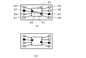
図2を参照して、図1のSiP設計支援装置1の動作の一例を説明する。図2は、図1のSiP設計支援装置1による端子の位置変更の一例を示す図であり、変更前と変更後のSiP基板21のPAD25〜39とLSIチップ23のチップ端子の間の接続状態を示す図である。図2(a)は変更前のPADとチップ端子の接続状態の一例を示す図であり、図2(b)は変更後のPADとチップ端子の接続状態の一例を示す図である。
An example of the operation of the SiP
図2(a)を参照して、SiP基板21上にはLSIチップ23が配置され、SiP基板21には、LSIチップ23を挟んで、一方に4つのPAD25、27、29、31があり、他方に4つのPAD33、35、37、39がある。SiP基板21のPAD25〜39とLSIチップ23のチップ端子とは、6つのPAD25、29、31、33、35、39はそれぞれ最も近いチップ端子と接続されているが、PAD27はPAD37に最も近いチップ端子41と接続され、PAD37はPAD27に最も近いチップ端子43と接続されている。
Referring to FIG. 2A, an
図2(a)のような接続状態において、PAD27とPAD37の位置を交換するか、またはチップ端子41とチップ端子43の位置を交換することにより、図2(b)にあるように、SiP基板のPADとLSIチップのチップ端子間の接続がトータルで最短となる。図1のSiP設計支援装置1は、このようなPADやチップ端子の位置を変更する処理を行うものである。
In the connected state as shown in FIG. 2A, the positions of the
続いて、図3を参照して、図1のSiP設計支援装置1の動作の一例を説明する。図3は、図1のSiP設計支援装置1の動作の一例を示すフロー図である。
Next, an example of the operation of the SiP
まず、図1の制御部3は、初期設定を行う(図3のステップSTM1)。この初期設定は、例えば、引数をチェックしたり、パラメータファイルや入力ファイルやコントロールファイルを読み込んだりすることにより行われる。
First, the
次に、図1の端子処理部5は、PADやチップ端子の位置を変更する処理を行う(図3のステップSTM2)。このPADやチップ端子の位置を変更する処理については、図4〜図12を用いてその一例を後述する。
Next, the
次に、図1の自動再配線処理部7は、PADから基板上のVIA・端子まで自動再配線処理を行う(図3のステップSTM3)。この自動再配線処理については、図13を用いてその一例を後述する。そして、図3の処理を終了する。
Next, the automatic
続いて、図4を参照して、図3のステップSTM2の端子位置変更処理の一例を説明する。図4は、図3のステップSTM2の端子位置変更処理の一例を示すフロー図である。 Next, an example of the terminal position changing process in step STM2 in FIG. 3 will be described with reference to FIG. FIG. 4 is a flowchart showing an example of the terminal position changing process in step STM2 of FIG.
まず、図1の端子処理部5は、ユーザにより選択された交換対象の端子がPADであるか否かの判断を行う(図4のステップSTE1)。交換対象の端子がPADであるならば図4のステップSTE2の処理を行い、PADでないならば図4のステップSTE5の処理を行う。
First, the
図4のステップSTE2において、図1の端子処理部5は、交換先が指定されているか否かの判断を行う。指定されているのであるならば図4のステップSTE4の処理を行い、指定されていないならば図4のステップSTE3の処理を行う。
In step STE2 of FIG. 4, the
図4のステップSTE3において、図1のPAD変換先決定処理部9は、PAD交換先決定処理を行う。このPAD交換先決定処理については、図5〜図8を用いてその一例を後述する。そして、図4のステップSTE4の処理を行う。
In step STE3 in FIG. 4, the PAD conversion destination
図4のステップSTE4において、図1のPAD位置変更処理部17は、PAD位置変更処理を行う。このPAD位置変更処理については、図9〜図12を参照してその一例を後述する。そして、図1の端子処理部5は図4の処理を終了する。
In step STE4 in FIG. 4, the PAD position
図4のステップSTE5において、図1の端子処理部5は、交換先が指定されているか否かの判断を行う。指定されているのであるならば図4のステップSTE7の処理を行い、指定されていないならば図4のステップSTE6の処理を行う。
In step STE5 in FIG. 4, the
図4のステップSTE6において、図1の端子変換先決定処理部13は、チップ端子交換先決定処理を行う。このチップ端子交換先決定処理は、図4のステップSTE3のPAD交換先決定処理と同様のものである。そして、図4のステップSTE7の処理を行う。
In step STE6 in FIG. 4, the terminal conversion destination
図4のステップSTE7において、図1のチップ端子位置変更処理部19は、チップ端子位置変更処理を行う。このチップ端子位置変更処理は、図4のステップSTE4のPAD位置変更処理と同様のものである。そして、図1の端子処理部5は図4の処理を終了する。
In step STE7 in FIG. 4, the chip terminal position
続いて、図5から図8を参照して、図4のステップSTE3のPAD交換先決定処理の一例を説明する。このPAD交換先決定処理においては、選択されたPADが一つである場合、選択された交換対象のPADに対して交換先のPADが自動的に決定される。交換先のPADは、例えば図7を用いて説明されるスペーシングルールや図8を用いて説明される平行配線長ルールなどのルールに基づいて決定される。このとき、特定のネットを指定することにより、ワイヤ結線後に指定されたネットのワイヤと交差するようなPADが交換相手として認識される。なお、指定されたネットのPADはFIX属性となり、他のPADとの交換対象にはならないとする。 Next, an example of the PAD exchange destination determination process in step STE3 in FIG. 4 will be described with reference to FIGS. In this PAD exchange destination determination process, when there is one selected PAD, an exchange destination PAD is automatically determined for the selected PAD to be exchanged. The replacement PAD is determined based on rules such as a spacing rule described with reference to FIG. 7 and a parallel wiring length rule described with reference to FIG. At this time, by designating a specific net, a PAD that intersects the wire of the designated net after wire connection is recognized as an exchange partner. Note that the PAD of the designated net has a FIX attribute and is not subject to exchange with another PAD.
図5は、図4のステップSTE3のPAD交換先決定処理の一例を示すフロー図である。 FIG. 5 is a flowchart showing an example of the PAD exchange destination determination process in step STE3 of FIG.
まず、図1のPAD交換先決定処理部13は、選択された交換対象のPADをPAD_Aとする(図5のステップSTT1)。
First, the PAD exchange destination
次に、図1のPAD交換先決定処理部13は、未処理のPADから所定の順にPADを取得して、取得したPADをPAD_Bとする(図5のステップSTT2)。取得する順は、例えばPAD_Aに近い順や優先度指定があれば優先度の順などである。
Next, the PAD exchange destination
次に、図1のPAD交換先決定処理部13は、指定ネットがあり、かつ、PAD_Bの場所からPAD_Aのワイヤを結線すると指定ネットのワイヤと交差しないか否かの判断を行う(図5のステップSTT3)。指定ネットがあって交差しないならば図5のステップSTT6の処理を行い、そうでないならば図5のステップSTT4の処理を行う。
Next, the PAD exchange destination
図5のステップSTT4において、図1のPAD交換先決定処理部13は、PAD_AとPAD_Bの交換可能性をチェックする。この交換可能性のチェックの処理については、図6を参照してその一例を後述する。
In step STT4 of FIG. 5, the PAD exchange destination
次に、図1のPAD交換先決定処理部13は、図5のステップSTT4の処理の結果に基づいてPAD_AとPAD_Bが交換可能であるか否かの判断を行う(図5のステップSTT5)。交換可能であるならば図5のステップSTT7の処理を行い、そうでないならば図5のステップSTT6の処理を行う。
Next, the PAD exchange destination
図5のステップSTT6において、図1のPAD交換先決定処理部13は、全PADに対して処理を行ったか否かの判断を行う。処理を行っているならばエラー終了をし、そうでないならば図5のステップSTT2の処理を行う。
In step STT6 in FIG. 5, the PAD exchange destination
図5のステップSTT7において、図1のPAD交換先決定処理部13は、PAD_Aの交換先としてPAD_Bを指定する。
In step STT7 of FIG. 5, the PAD exchange destination
次に、図1のPAD交換先決定処理部13は、指定ネットがあるか否かの判断を行う(図5のステップSTT8)。指定ネットがあるならば、該当ネットのPADをFIXとして(図5のステップSTT9)図5の処理を終了する。指定ネットがないならば、図5の処理を終了する。
Next, the PAD exchange destination
以上、図5のフロー図に示されるようにして、ユーザにより選択された交換対象のPADに対して交換先のPADが決定される。 As described above, as shown in the flowchart of FIG. 5, the exchange destination PAD is determined for the exchange target PAD selected by the user.
続いて、図6を参照して、図5のステップSTT4のPAD_AとPAD_Bの交換可能性のチェックの処理の一例を説明する。図6は、図5のステップSTT4のPAD_AとPAD_Bの交換可能性のチェックの処理の一例を示すフロー図である。 Next, an example of the process of checking the exchangeability of PAD_A and PAD_B in step STT4 in FIG. 5 will be described with reference to FIG. FIG. 6 is a flowchart showing an example of processing for checking the exchangeability of PAD_A and PAD_B in step STT4 of FIG.
まず、図1のPAD交換先決定処理部13は、ワイヤを仮削除する(図6のステップSTC1)。このワイヤの仮削除処理は、LSIチップの端子がPAD_A又はPAD_Bと接続されているときに、PAD_A又はPAD_Bと接続されているLINE(基板側のPADとLSI側の端子を結ぶ情報)に対して、ボンディングワイヤの情報(WIRE情報)であってLSIチップの端子(PORTINST)と接続されているものを仮に削除する処理である。
First, the PAD exchange destination
次に、図1のPAD交換先決定処理部13は、PAD_Bの位置をPAD_Aの新しい位置として仮配線する(図6のステップSTC2)。
Next, the PAD replacement destination
次に、図1のPAD交換先決定処理部13は、結線可能であるか否かを判断する(図6のステップSTC3)。結線可能であるならば図6のステップSTC4の処理を行い、そうでないならば図6のステップSTC8の処理を行う。この結線可能性の判断については、図7と図8を参照してその一例を後述する。
Next, the PAD exchange destination
図6のステップSTC4において、図1のPAD交換先決定処理部13は、結線したワイヤ長を上位ルーチンへ戻す。次に、結線したワイヤ形状を上位ルーチンへ戻す(図6のステップSTC5)。次に、仮に削除されたワイヤを復元し(図6のステップSTC6)、PAD_AとPAD_Bは交換可能と判断して(図6のステップSTC7)、図6の処理を終了する。
In step STC4 in FIG. 6, the PAD exchange destination
図6のステップSTC8において、図1のPAD交換先決定処理部13は、仮に削除されたワイヤを復元する。次に、PAD_AとPAD_Bは交換可能でないと判断し(図6のステップSTC9)、図6の処理を終了する。
In step STC8 of FIG. 6, the PAD exchange destination
以上、図6のフロー図に示されるようにして、PAD_AとPAD_Bの交換可能性がチェックされる。 As described above, the exchangeability of PAD_A and PAD_B is checked as shown in the flowchart of FIG.
続いて、図7と図8を参照して、図6のステップSTC3の結線可能性の判断についてその一例を説明する。 Next, with reference to FIG. 7 and FIG. 8, an example of the determination of the connection possibility in step STC3 of FIG. 6 will be described.
図7は、新規に作成する三次元空間内のボンデングワイヤを示す図である。図7を参照して、スペーシングルール、すなわち、配置されるLSIチップの端子から基板上のPADへのボンディングワイヤの間隔に関するルールについて説明する。 FIG. 7 is a diagram illustrating a bonding wire in a three-dimensional space that is newly created. With reference to FIG. 7, the spacing rule, that is, the rule relating to the bonding wire interval from the terminal of the arranged LSI chip to the PAD on the substrate will be described.
図7を参照して、新規に作成する三次元空間内のボンデングワイヤ座標をP0、P1、P2、P3、P4とする。そして、他のワイヤと線分P1−P2、P2−P3、P3−P4の距離を求め、求めた距離の最小値を他ワイヤと線分P1−P2、P2−P3、P3−P4間の距離とする。 Referring to FIG. 7, bond wire coordinates in a newly created three-dimensional space are P0, P1, P2, P3, and P4. Then, the distances between the other wires and the line segments P1-P2, P2-P3, P3-P4 are obtained, and the minimum value of the obtained distances is the distance between the other wires and the line segments P1-P2, P2-P3, P3-P4. And
新規ボンデングワイヤと他ワイヤ間の距離が指定された距離より短い場合、スペーシングルールエラーとなりワイヤは結線できないとする。このように、他ワイヤとのスペーシングルールが指定され、このルールを満たした形状計算が行われる。 If the distance between the new bonding wire and the other wire is shorter than the specified distance, a spacing rule error occurs and the wire cannot be connected. In this way, a spacing rule with other wires is specified, and shape calculation satisfying this rule is performed.
続いて、図8を参照して、平行配線長ルール、すなわち、配置されるLSIチップの端子から基板上のPADへのボンディングワイヤが複数あるときに、指定されるワイヤ同士が平行に配線される距離の最小値に関するルールについて説明する。図8は、ワイヤ形状計算を行う際に他のワイヤに対する平行部分の長さを示す図である。平行部分の長さは、形状計算したワイヤA0−A1と他のワイヤB0−B1が三次元的に平行でかつ一定距離以内にある場合に計算される。図8において、点A0及び点A1並びに点B0及び点B1は、ベクトルA0A1とベクトルB0B1が同じ向きになるような点であり、点B0’及び点B1’は、それぞれ、点B0と点B1が直線A0−A1上に直線A0−A1と垂直方向に射影された点である。 Subsequently, referring to FIG. 8, when there are a plurality of bonding wires from the terminals of the LSI chip to be arranged to the PAD on the substrate, the designated wires are wired in parallel. A rule regarding the minimum value of the distance will be described. FIG. 8 is a diagram showing the length of a parallel portion with respect to another wire when performing wire shape calculation. The length of the parallel portion is calculated when the wire A0-A1 whose shape has been calculated and the other wires B0-B1 are three-dimensionally parallel and within a certain distance. In FIG. 8, point A0 and point A1, point B0 and point B1 are points such that vector A0A1 and vector B0B1 are in the same direction, and point B0 ′ and point B1 ′ are point B0 and point B1, respectively. This is a point projected on the straight line A0-A1 in a direction perpendicular to the straight line A0-A1.
図8(a)は、線分A0−A1上に点B1’があって点B0’がない場合の、線分A0−A1と線分B0−B1の平行部分の長さ|A0−B1’|を示す図である。図8(a)を参照して、平行部分の長さ|A0−B1’|の計算方法について説明する。 FIG. 8A shows the length | A0-B1 ′ of the parallel part of the line segment A0-A1 and the line segment B0-B1 when the point B1 ′ is present on the line segment A0-A1 and there is no point B0 ′. FIG. With reference to FIG. 8A, a method of calculating the length | A0−B1 ′ | of the parallel portion will be described.
図8(a)を参照して、ベクトルA0A1をその長さで割って求められる単位ベクトルをベクトルeとし、ベクトルxとベクトルyの内積を(x,y)とすると、平行部分の長さ|A0−B1’|は、|(ベクトルA0B1,ベクトルe)|により求められる。 Referring to FIG. 8A, if a unit vector obtained by dividing vector A0A1 by its length is vector e and the inner product of vector x and vector y is (x, y), the length of the parallel portion | A0−B1 ′ | is obtained by | (vector A0B1, vector e) |.
点A0、A1、B0’、B1’の位置関係は、6通りある。以下では、図8(b)〜(e)を参照して、それぞれの場合の平行部分の長さについて説明する。 There are six positional relationships between the points A0, A1, B0 ', and B1'. Below, with reference to FIG.8 (b)-(e), the length of the parallel part in each case is demonstrated.
図8(b)を参照して、線分A0−A1が線分B0’−B1’を含む場合、すなわち、(A0B0,e)>=0、(A0B1,e)>0、(A1B0’,e)<0、(A1B0,e)<=0の場合、平行部分の長さは線分B0’−B1’の長さである。 Referring to FIG. 8B, when line segment A0-A1 includes line segment B0′-B1 ′, that is, (A0B0, e)> = 0, (A0B1, e)> 0, (A1B0 ′, e) When <0, (A1B0, e) <= 0, the length of the parallel portion is the length of the line segment B0′-B1 ′.
図8(c)を参照して、線分A0−A1に点B0’があって点B1’がない場合、すなわち、(A0B0,e)>=0、(A0B1,e)>0、(A1B0’,e)<0、(A1B0,e)>=0の場合、平行部分の長さは線分B0’−A1の長さである。 Referring to FIG. 8C, when the line segment A0-A1 has a point B0 'and no point B1', that is, (A0B0, e)> = 0, (A0B1, e)> 0, (A1B0 When ', e) <0 and (A1B0, e)> = 0, the length of the parallel portion is the length of the line segment B0′-A1.
同様に、線分A0−A1の間に点B1’があって点B0’がない場合、すなわち、(A0B0,e)<=0、(A0B1,e)>0、(A1B0’,e)<0、(A1B0,e)<=0の場合、平行部分の長さは線分A0−B1’の長さである。 Similarly, when there is a point B1 ′ between the line segments A0-A1 and no point B0 ′, that is, (A0B0, e) <= 0, (A0B1, e)> 0, (A1B0 ′, e) < When 0 and (A1B0, e) <= 0, the length of the parallel portion is the length of the line segment A0-B1 ′.
図8(d)を参照して、線分A0−A1と線分B0’−B1’が重ならない場合、すなわち、(A0B0,e)>=0、(A0B1,e)>0、(A1B0’,e)>0、(A1B0,e)>=0の場合、平行部分の長さは0である。 Referring to FIG. 8D, when the line segment A0-A1 and the line segment B0'-B1 'do not overlap, that is, (A0B0, e)> = 0, (A0B1, e)> 0, (A1B0' , E)> 0 and (A1B0, e)> = 0, the length of the parallel portion is zero.
同様に、線分A0−A1と線分B0’−B1’が重ならない場合、すなわち、(A0B0,e)<=0、(A0B1,e)<0、(A1B0’,e)<0、(A1B0,e)<=0の場合、平行部分の長さは0である。 Similarly, when the line segment A0-A1 and the line segment B0′-B1 ′ do not overlap, that is, (A0B0, e) <= 0, (A0B1, e) <0, (A1B0 ′, e) <0, When A1B0, e) <= 0, the length of the parallel part is zero.
図8(e)を参照して、線分A0−A1が線分B0’−B1’に含まれる場合、すなわち、(A0B0,e)<=0、(A0B1,e)>0、(A1B0’,e)<0、(A1B0,e)>=0の場合、平行部分の長さは線分A0−A1の長さである。 Referring to FIG. 8E, when line segment A0-A1 is included in line segment B0′-B1 ′, that is, (A0B0, e) <= 0, (A0B1, e)> 0, (A1B0 ′ , E) <0, (A1B0, e)> = 0, the length of the parallel portion is the length of the line segment A0-A1.
以上のようにして、平行部分の長さが計算される。この長さが指定された値より大きい場合、平行配線長エラーとなり、ワイヤは結線できないと判断される。 As described above, the length of the parallel portion is calculated. If this length is greater than the specified value, a parallel wiring length error occurs and it is determined that the wire cannot be connected.
続いて、図9と図10を参照して、図4のステップSTE4のPAD位置変更処理の一例を説明する。図9と図10は、図4のステップSTE4のPAD位置変更処理の一例を示すフロー図である。図9と図10においては、交換対象のPADの移動により押しのけられたPADの位置が最適になるように、他のPADの位置が変更される。そして、このとき変更されたPADの位置が再び最適になるように他のPADの位置が変更される。この処理を繰り返すことにより、必要最低限のPADのみが位置変更される。なお、一度位置が決められたPADは動かされないものとする。 Next, an example of the PAD position change process in step STE4 in FIG. 4 will be described with reference to FIGS. 9 and 10 are flowcharts showing an example of the PAD position change process in step STE4 of FIG. 9 and 10, the positions of the other PADs are changed so that the position of the PAD pushed away by the movement of the PAD to be exchanged becomes optimum. Then, the positions of other PADs are changed so that the positions of the PADs changed at this time are optimized again. By repeating this process, only the minimum necessary PAD is repositioned. It is assumed that the PAD once positioned is not moved.
まず、図1のPAD位置変更処理部17は、交換対象のPADをPAD_Aとし、交換先のPADをPAD_Bとする(図9のステップSTP1)。
First, the PAD position
次に、図1のPAD位置変更処理部17は、PAD_AとPAD_Bの位置を交換する(図9のステップSTP2)。このPADの位置を交換する処理については、図11を用いてその一例を後述する。
Next, the PAD position
次に、図1のPAD位置変更処理部17は、指定ネットがあり、かつ、指定ネットのPADはFIXでないか否かの判断を行う(図9のステップSTP3)。指定ネットがあって指定ネットのPADがFIXでないならば図9のステップSTP5の処理を行い、そうでないならば図9のステップSTP4の処理を行う。
Next, the PAD position
図9のステップSTP4において、図1のPAD位置変更処理部17は、PAD_Bの位置変更処理を行う。このPADの位置変更処理については、図12を用いてその一例を後述する。そして、図9と図10の処理を終了する。
In step STP4 in FIG. 9, the PAD position
図9のステップSTP5において、図1のPAD位置変更処理部17は、指定ネットのワイヤが交換したPAD_Aのワイヤと交差するか否かの判断をする。交差するならば図9のステップSTP6の処理を行い、そうでないならば図10のステップSTP7の処理を行う。
In step STP5 of FIG. 9, the PAD position
図9のステップSTP6において、図1のPAD位置変更処理部17は、指定ネットのPADをFIXとする。そして、図9と図10の処理を終了する。
In step STP6 in FIG. 9, the PAD position
図10のステップSTP7において、図1のPAD位置変更処理部17は、未処理のPADから所定の順にPADを取得して、取得したPADをPAD_Cとする。取得する順は、例えば、PAD_Aに近い順や、優先度指定があれば優先度の順などである。
In step STP7 in FIG. 10, the PAD position
次に、図1のPAD位置変更処理部17は、指定ネット端子とPAD_Cを結ぶワイヤはPAD_Aのワイヤと交差するか否かを判断する(図10のステップSTP8)。交差するならば図10のステップSTP9の処理を行い、そうでないならば図10のステップSTP7の処理を行う。
Next, the PAD position
図10のステップSTP9において、図1のPAD位置変更処理部17は、PAD_Cと指定ネットの端子間でワイヤを結線する。
In step STP9 in FIG. 10, the PAD position
次に、図1のPAD位置変更処理部17は、図10のステップSTP9で結線をすることができたか否かの判断を行う(図10のステップSTP10)。結線できたならば図10のステップSTP11の処理を行い、そうでないならば図10のステップSTP7の処理を行う。
Next, the PAD position
図10のステップSTP11において、図1のPAD位置変更処理部17は、PAD_Cと指定ネットのPADの位置を交換する。次に、指定ネットのPADをFIXとする(図10のステップSTP12)。
In step STP11 in FIG. 10, the PAD position
次に、図1のPAD位置変更処理部17は、指定ネットのワイヤが結線できたか否かの判断を行う(図10のステップSTP13)。結線できたならば、PAD_Bの位置変更処理を行い(図10のステップSTP14)、PAD_Cの位置変更処理を行い(図10のステップSTP15)、図9と図10の処理を終了する。図10のステップSTP14とステップSTP15の位置変更処理は、図9のステップSTP4のPADの位置変更処理と同様のものである。結線できないならば、図9と図10の処理を終了する。
Next, the PAD position
以上、図9と図10のフロー図に示されるようにして、図4のステップSTE4のPADの位置の変更処理が行われる。 As described above, as shown in the flowcharts of FIGS. 9 and 10, the PAD position changing process in step STE4 of FIG. 4 is performed.
続いて、図11を参照して、図9のステップSTP2のPAD_AとPAD_Bの交換処理の一例を説明する。図11は、図9のステップSTP2の処理の一例を示すフロー図である。 Next, an example of the PAD_A and PAD_B exchange process in step STP2 in FIG. 9 will be described with reference to FIG. FIG. 11 is a flowchart showing an example of the process of step STP2 of FIG.
まず、図1のPAD位置変更処理部17は、接続点変更処理を行う(図11のステップSTW1)。具体的には、まず、PAD_Aと接続されているLINEに対して、PAD_Bの位置をPAD_Aの新しい位置として、PAD_A−>NET−>LINEの接続点変更し、WIRE情報があり、PORTINSTと接続されているならば、PAD_A−>NET−>LINE(−>WIRE)をfreeする。また、PAD_Bと接続されているLINEに対して、PAD_Aの位置をPAD_Bの新しい位置として、PAD_B−>NET−>LINEの接続点変更する。
First, the PAD position
次に、図1のPAD位置変更処理部17は、PAD_Aの電気的な接続をPAD_Bと交換し(図11のステップSTW2)、PAD_Bの電気的な接続をPAD_Aと交換する(図11のステップSTW3)。次に、図1のPAD位置変更処理部17は、PAD_AとPAD_Bが交換したことを格納する(図11のステップSTW4)。そして、図11の処理を終了する。
Next, the PAD position
続いて、図12を参照して、図9のステップSTP4のPADの位置変更処理を説明する。図12は、図9のステップSTP4のPAD_Bの位置変更処理の一例を示すフロー図である。 Next, the PAD position changing process in step STP4 of FIG. 9 will be described with reference to FIG. FIG. 12 is a flowchart showing an example of the position change process of PAD_B in step STP4 of FIG.
まず、図1のPAD位置変更処理部17は、全PADのうち、PAD_Bと交換可能なPAD(以下ではこのようなPADをPAD_Yという)があれば、PAD_Bのワイヤが一番短くなるようなPAD_Yと、そのときのPAD_Bのワイヤ形状を記憶する(図12のステップSTX1)。
First, the PAD position
次に、図1のPAD位置変更処理部17は、PAD_Yが見つかったか否かの判断を行う(図12のステップSTX2)。見つかったならば図12のステップSTX3の処理を行い、そうでないならば図12のステップSTX4の処理を行う。
Next, the PAD position
図12のステップSTX3において、図1のPAD位置変更処理部17は、PAD_Bと記憶されたPAD_Yの位置を交換する。そして、図12のステップSTX1の処理を行う。
In step STX3 in FIG. 12, the PAD position
図12のステップSTX4において、図1のPAD位置変更処理部17は、PAD_Bに元々繋がっていたワイヤがルールを守っているか否かの判断を行う。ルールを守っていたならば、ワイヤを作成し(図12のステップSTX5)、図12の処理を終了する。そうでないならば、警告をして(図12のステップSTX6)、図12の処理を終了する。
In step STX4 in FIG. 12, the PAD position
続いて、図13を参照して、図1の自動再配線処理部7による図3のステップSTM3の自動再配線処理の一例を説明する。図13は、図3のステップSTM3の自動再配線処理の一例を示すフロー図である。
Next, an example of the automatic rewiring process in step STM3 in FIG. 3 by the
まず、図1の自動再配線処理部7は、コントロールファイルの基板のゾーンと接続するLAYERの配線幅によって(最大公約数)、配線グリッドと配線禁止領域を作成する(図13のステップSTR1)。
First, the automatic
次に、図1の自動再配線処理部7は、入れ換えが生じたPADについて、既配線削除処理と基板配線処理を行う(図13のステップSTR2)。ここで、既配線削除処理は、NETが基板配線のときに配線図形を削除する処理であり、基板配線処理は、NETが基板配線のときに、基板配線のパスを迷路法により探し、一番短いパスによってLINEを作成し、LINEをNETの配線図形とするものである。
Next, the automatic
次に、図1の自動再配線処理部7は、配線グリッドを削除する(図13のステップSTR3)。そして、図13の処理を終了する。
Next, the automatic
以上のようにして、図1のSiP設計支援装置1は、基板の端子の位置とチップの端子の位置を同時に変更し、自動的に再配線処理をすることができる。
As described above, the SiP
なお、基板上のPADとLSIチップの端子の位置変更に関しては、図4に示されるようにどちらかを固定して他方を移動するだけでなく、両方を自動に動かしてもよい。すなわち、例えば一方(例えば基板上のPAD)を変更することにより、他方(例えばLSIチップの端子)を変更するようにしてもよい。 Regarding the change of the position of the terminals of the PAD and the LSI chip on the substrate, as shown in FIG. 4, not only one of them may be fixed and the other may be moved, but both may be moved automatically. That is, for example, by changing one (for example, PAD on a substrate), the other (for example, a terminal of an LSI chip) may be changed.
1 SiP設計支援装置
3 制御部
5 端子位置変更処理部
7 自動再配線処理部
9 PAD交換先決定処理部
11 PAD位置変更処理部
13 チップ端子交換先決定処理部
15 チップ端子位置変更処理部
DESCRIPTION OF
Claims (10)
前記基板又は前記チップの端子について、
当該端子の位置を変更することにより、当該端子に接続する配線の少なくとも一つが他の配線の少なくとも一つと交差する場合に、当該端子の位置が変更可能かどうかを調べ、変更可能な場合に当該端子の位置を変更し、
当該端子の位置を変更することにより、当該端子に接続する配線が他の配線と交差しない場合には、当該端子の位置を変更しない端子位置変更手段を備える半導体装置設計支援装置。 A semiconductor device design support apparatus for supporting a design of a semiconductor device having a substrate and a chip disposed on the substrate, wherein a terminal of the substrate and a terminal of the chip are connected by electrical wiring,
For the terminals of the substrate or the chip,
By changing the position of the terminal, when at least one of the wiring connected to the terminal intersects with at least one other wiring, examine the position of the terminal is if we can change, the if it can be modified Change the terminal position ,
A semiconductor device design support apparatus comprising terminal position changing means that does not change the position of a terminal when the wiring connected to the terminal does not intersect with another wiring by changing the position of the terminal.
前記基板の端子の位置を変更する基板端子位置変更処理手段と、
前記チップの端子の位置を変更するチップ端子位置変更処理手段
を有する、請求項1又は2に記載の半導体装置設計支援装置。 The terminal position changing means is
Board terminal position change processing means for changing the position of the terminal of the board;
The semiconductor device design support apparatus according to claim 1, further comprising a chip terminal position change processing unit that changes a position of a terminal of the chip.
前記端子位置変更手段は、前記交換対象の端子の位置と前記端子交換先決定処理手段により決定された前記交換先の端子の位置を交換する、
請求項1から4のいずれかに記載の半導体装置設計支援装置。 A terminal replacement destination determination processing means for determining a replacement destination terminal that satisfies a predetermined condition for a specified replacement target terminal;
The terminal position changing means exchanges the position of the terminal to be exchanged and the position of the exchange destination terminal determined by the terminal exchange destination decision processing means,
The semiconductor device design support apparatus according to claim 1.
前記基板又は前記チップの2つの第1及び第2の端子について、
前記第1の端子と前記第2の端子の位置を交換した場合に、前記第1の端子及び前記第2の端子に接続する配線の少なくとも一つが他の配線の少なくとも一つと交差するときに、前記第1及び前記第2の端子の位置が交換可能かどうかを調べ、交換可能な場合に前記第1及び前記第2の端子の位置を交換し、
前記第1の端子と前記第2の端子の位置を交換した場合に、前記第1の端子及び前記第2の端子に接続する配線が他の配線と交差しないときには、前記第1及び前記第2の端子の位置を交換しない端子位置変更手段を備える半導体装置設計支援装置。 A semiconductor device design support apparatus for supporting a design of a semiconductor device having a substrate and a chip disposed on the substrate, wherein a terminal of the substrate and a terminal of the chip are connected by electrical wiring,
For the two first and second terminals of the substrate or the chip,
When the positions of the first terminal and the second terminal are exchanged, when at least one of the wirings connected to the first terminal and the second terminal intersects with at least one of the other wirings, determine whether the position of the first and the second terminal is replaceable, to swap the position of said first and said second terminal when replaceable,
When the positions of the first terminal and the second terminal are exchanged, and the wiring connected to the first terminal and the second terminal does not intersect with the other wiring, the first and second A semiconductor device design support apparatus comprising terminal position changing means that does not exchange the positions of the terminals .
端子位置変更手段が、前記基板又は前記チップの端子について、
当該端子の位置を変更することにより、当該端子に接続する配線の少なくとも一つが他の配線の少なくとも一つと交差する場合に、当該端子の位置が変更可能かどうかを調べ、変更可能な場合に当該端子の位置を変更し、
当該端子の位置を変更することにより、当該端子に接続する配線が他の配線と交差しない場合には、当該端子の位置を変更しないステップを含む半導体装置設計支援方法。 A semiconductor device design support method for supporting a design of a semiconductor device having a substrate and a chip disposed on the substrate, wherein a terminal of the substrate and a terminal of the chip are connected by electrical wiring,
The terminal position changing means is the terminal of the substrate or the chip,
By changing the position of the terminal, when at least one of the wiring connected to the terminal intersects with at least one other wiring, examine the position of the terminal is if we can change, the if it can be modified Change the terminal position ,
A semiconductor device design support method including a step of not changing a position of a terminal when the wiring connected to the terminal does not intersect with another wiring by changing the position of the terminal .
Priority Applications (1)
| Application Number | Priority Date | Filing Date | Title |
|---|---|---|---|
| JP2005289296A JP4663473B2 (en) | 2005-09-30 | 2005-09-30 | Semiconductor device design support apparatus, semiconductor device design support method, program capable of executing the method by computer, and recording medium recording the program |
Applications Claiming Priority (1)
| Application Number | Priority Date | Filing Date | Title |
|---|---|---|---|
| JP2005289296A JP4663473B2 (en) | 2005-09-30 | 2005-09-30 | Semiconductor device design support apparatus, semiconductor device design support method, program capable of executing the method by computer, and recording medium recording the program |
Publications (2)
| Publication Number | Publication Date |
|---|---|
| JP2007102381A JP2007102381A (en) | 2007-04-19 |
| JP4663473B2 true JP4663473B2 (en) | 2011-04-06 |
Family
ID=38029283
Family Applications (1)
| Application Number | Title | Priority Date | Filing Date |
|---|---|---|---|
| JP2005289296A Expired - Fee Related JP4663473B2 (en) | 2005-09-30 | 2005-09-30 | Semiconductor device design support apparatus, semiconductor device design support method, program capable of executing the method by computer, and recording medium recording the program |
Country Status (1)
| Country | Link |
|---|---|
| JP (1) | JP4663473B2 (en) |
Families Citing this family (2)
| Publication number | Priority date | Publication date | Assignee | Title |
|---|---|---|---|---|
| JP4384230B2 (en) | 2008-03-19 | 2009-12-16 | ダイハツ工業株式会社 | Engine cooling system |
| JP2010102401A (en) | 2008-10-21 | 2010-05-06 | Toshiba Corp | Routing design method, routing design apparatus, and routing design program |
Citations (4)
| Publication number | Priority date | Publication date | Assignee | Title |
|---|---|---|---|---|
| JPH05326836A (en) * | 1992-05-18 | 1993-12-10 | Mitsubishi Electric Corp | Layout design supporting device |
| JP2001060625A (en) * | 1999-08-19 | 2001-03-06 | Nec Ic Microcomput Syst Ltd | Retrieval of chip pad |
| JP2001209667A (en) * | 2000-01-26 | 2001-08-03 | Internatl Business Mach Corp <Ibm> | Method and device for automatically generating multi- terminal net, and program storage medium having program for executing automatic multi-terminal net generation method stored therein |
| JP2004047829A (en) * | 2002-07-12 | 2004-02-12 | Toshiba Corp | Device and method for designing connection terminal for semiconductor device, and program for designing the same |
-
2005
- 2005-09-30 JP JP2005289296A patent/JP4663473B2/en not_active Expired - Fee Related
Patent Citations (4)
| Publication number | Priority date | Publication date | Assignee | Title |
|---|---|---|---|---|
| JPH05326836A (en) * | 1992-05-18 | 1993-12-10 | Mitsubishi Electric Corp | Layout design supporting device |
| JP2001060625A (en) * | 1999-08-19 | 2001-03-06 | Nec Ic Microcomput Syst Ltd | Retrieval of chip pad |
| JP2001209667A (en) * | 2000-01-26 | 2001-08-03 | Internatl Business Mach Corp <Ibm> | Method and device for automatically generating multi- terminal net, and program storage medium having program for executing automatic multi-terminal net generation method stored therein |
| JP2004047829A (en) * | 2002-07-12 | 2004-02-12 | Toshiba Corp | Device and method for designing connection terminal for semiconductor device, and program for designing the same |
Also Published As
| Publication number | Publication date |
|---|---|
| JP2007102381A (en) | 2007-04-19 |
Similar Documents
| Publication | Publication Date | Title |
|---|---|---|
| US7496878B2 (en) | Automatic wiring method and apparatus for semiconductor package and automatic identifying method and apparatus for semiconductor package | |
| EP0145925A2 (en) | Iterative method for establishing connections between nodes and the resulting product | |
| JPH10270563A (en) | Automatic general wiring method for integrated circuit | |
| US6245599B1 (en) | Circuit wiring system circuit wiring method semi-conductor package and semi-conductor package substrate | |
| JP4443450B2 (en) | Automatic wiring determination device | |
| US8225268B2 (en) | Wiring design method for wiring board | |
| US7216325B2 (en) | Semiconductor device, routing method and manufacturing method of semiconductor device | |
| JP4663473B2 (en) | Semiconductor device design support apparatus, semiconductor device design support method, program capable of executing the method by computer, and recording medium recording the program | |
| US9928334B2 (en) | Redistribution layer routing for integrated fan-out wafer-level chip-scale packages | |
| JP4562625B2 (en) | Automatic wiring determination method and computer program for causing a computer to execute the automatic wiring determination process | |
| JP4311244B2 (en) | Wiring route determination method and system | |
| Kubo et al. | Global routing by iterative improvements for two-layer ball grid array packages | |
| JP5380969B2 (en) | Layout design method and apparatus | |
| JP4549094B2 (en) | Clearance inspection apparatus and method | |
| JP5900540B2 (en) | Layout design method and layout design support program | |
| JP5187217B2 (en) | Semiconductor layout system, method, and program | |
| JP4275722B2 (en) | Wiring design method | |
| Lee et al. | Board-and chip-aware package wire planning | |
| JP2006294707A (en) | Semiconductor integrated circuit and method of wiring the same | |
| JP2001298089A (en) | Method of designing semiconductor integrated circuit | |
| JP5672341B2 (en) | Layout design method, apparatus and program | |
| JP2002215704A (en) | Method and device for determining terminal position in module | |
| JPH087759B2 (en) | Automatic component placement processing method | |
| JP2009130228A (en) | Layout designing method, layout design program, and layout design apparatus | |
| JP2003249591A (en) | Method for designing wiring board of area io type semiconductor device |
Legal Events
| Date | Code | Title | Description |
|---|---|---|---|
| A621 | Written request for application examination |
Free format text: JAPANESE INTERMEDIATE CODE: A621 Effective date: 20080911 |
|
| A977 | Report on retrieval |
Free format text: JAPANESE INTERMEDIATE CODE: A971007 Effective date: 20100701 |
|
| A131 | Notification of reasons for refusal |
Free format text: JAPANESE INTERMEDIATE CODE: A131 Effective date: 20100707 |
|
| A521 | Written amendment |
Free format text: JAPANESE INTERMEDIATE CODE: A523 Effective date: 20100903 |
|
| A131 | Notification of reasons for refusal |
Free format text: JAPANESE INTERMEDIATE CODE: A131 Effective date: 20100921 |
|
| RD02 | Notification of acceptance of power of attorney |
Free format text: JAPANESE INTERMEDIATE CODE: A7422 Effective date: 20101001 |
|
| A521 | Written amendment |
Free format text: JAPANESE INTERMEDIATE CODE: A523 Effective date: 20101119 Free format text: JAPANESE INTERMEDIATE CODE: A821 Effective date: 20101119 |
|
| TRDD | Decision of grant or rejection written | ||
| A01 | Written decision to grant a patent or to grant a registration (utility model) |
Free format text: JAPANESE INTERMEDIATE CODE: A01 Effective date: 20101214 |
|
| A01 | Written decision to grant a patent or to grant a registration (utility model) |
Free format text: JAPANESE INTERMEDIATE CODE: A01 |
|
| A61 | First payment of annual fees (during grant procedure) |
Free format text: JAPANESE INTERMEDIATE CODE: A61 Effective date: 20110105 |
|
| R150 | Certificate of patent or registration of utility model |
Free format text: JAPANESE INTERMEDIATE CODE: R150 |
|
| FPAY | Renewal fee payment (event date is renewal date of database) |
Free format text: PAYMENT UNTIL: 20140114 Year of fee payment: 3 |
|
| R250 | Receipt of annual fees |
Free format text: JAPANESE INTERMEDIATE CODE: R250 |
|
| R250 | Receipt of annual fees |
Free format text: JAPANESE INTERMEDIATE CODE: R250 |
|
| LAPS | Cancellation because of no payment of annual fees |