JP4662474B2 - Data processing device - Google Patents
Data processing device Download PDFInfo
- Publication number
- JP4662474B2 JP4662474B2 JP2006033513A JP2006033513A JP4662474B2 JP 4662474 B2 JP4662474 B2 JP 4662474B2 JP 2006033513 A JP2006033513 A JP 2006033513A JP 2006033513 A JP2006033513 A JP 2006033513A JP 4662474 B2 JP4662474 B2 JP 4662474B2
- Authority
- JP
- Japan
- Prior art keywords
- data strobe
- strobe signal
- signal circuit
- inverted data
- terminal
- Prior art date
- Legal status (The legal status is an assumption and is not a legal conclusion. Google has not performed a legal analysis and makes no representation as to the accuracy of the status listed.)
- Active
Links
Images


Classifications
-
- G—PHYSICS
- G11—INFORMATION STORAGE
- G11C—STATIC STORES
- G11C5/00—Details of stores covered by group G11C11/00
- G11C5/02—Disposition of storage elements, e.g. in the form of a matrix array
- G11C5/04—Supports for storage elements, e.g. memory modules; Mounting or fixing of storage elements on such supports
-
- G—PHYSICS
- G11—INFORMATION STORAGE
- G11C—STATIC STORES
- G11C5/00—Details of stores covered by group G11C11/00
- G11C5/02—Disposition of storage elements, e.g. in the form of a matrix array
-
- G—PHYSICS
- G11—INFORMATION STORAGE
- G11C—STATIC STORES
- G11C5/00—Details of stores covered by group G11C11/00
- G11C5/06—Arrangements for interconnecting storage elements electrically, e.g. by wiring
-
- G—PHYSICS
- G11—INFORMATION STORAGE
- G11C—STATIC STORES
- G11C5/00—Details of stores covered by group G11C11/00
- G11C5/06—Arrangements for interconnecting storage elements electrically, e.g. by wiring
- G11C5/063—Voltage and signal distribution in integrated semi-conductor memory access lines, e.g. word-line, bit-line, cross-over resistance, propagation delay
-
- H—ELECTRICITY
- H01—ELECTRIC ELEMENTS
- H01L—SEMICONDUCTOR DEVICES NOT COVERED BY CLASS H10
- H01L23/00—Details of semiconductor or other solid state devices
- H01L23/48—Arrangements for conducting electric current to or from the solid state body in operation, e.g. leads, terminal arrangements ; Selection of materials therefor
- H01L23/488—Arrangements for conducting electric current to or from the solid state body in operation, e.g. leads, terminal arrangements ; Selection of materials therefor consisting of soldered or bonded constructions
- H01L23/498—Leads, i.e. metallisations or lead-frames on insulating substrates, e.g. chip carriers
- H01L23/49811—Additional leads joined to the metallisation on the insulating substrate, e.g. pins, bumps, wires, flat leads
- H01L23/49816—Spherical bumps on the substrate for external connection, e.g. ball grid arrays [BGA]
-
- H—ELECTRICITY
- H01—ELECTRIC ELEMENTS
- H01L—SEMICONDUCTOR DEVICES NOT COVERED BY CLASS H10
- H01L23/00—Details of semiconductor or other solid state devices
- H01L23/48—Arrangements for conducting electric current to or from the solid state body in operation, e.g. leads, terminal arrangements ; Selection of materials therefor
- H01L23/488—Arrangements for conducting electric current to or from the solid state body in operation, e.g. leads, terminal arrangements ; Selection of materials therefor consisting of soldered or bonded constructions
- H01L23/498—Leads, i.e. metallisations or lead-frames on insulating substrates, e.g. chip carriers
- H01L23/49822—Multilayer substrates
-
- H—ELECTRICITY
- H01—ELECTRIC ELEMENTS
- H01L—SEMICONDUCTOR DEVICES NOT COVERED BY CLASS H10
- H01L23/00—Details of semiconductor or other solid state devices
- H01L23/48—Arrangements for conducting electric current to or from the solid state body in operation, e.g. leads, terminal arrangements ; Selection of materials therefor
- H01L23/488—Arrangements for conducting electric current to or from the solid state body in operation, e.g. leads, terminal arrangements ; Selection of materials therefor consisting of soldered or bonded constructions
- H01L23/498—Leads, i.e. metallisations or lead-frames on insulating substrates, e.g. chip carriers
- H01L23/49827—Via connections through the substrates, e.g. pins going through the substrate, coaxial cables
-
- H—ELECTRICITY
- H01—ELECTRIC ELEMENTS
- H01L—SEMICONDUCTOR DEVICES NOT COVERED BY CLASS H10
- H01L23/00—Details of semiconductor or other solid state devices
- H01L23/48—Arrangements for conducting electric current to or from the solid state body in operation, e.g. leads, terminal arrangements ; Selection of materials therefor
- H01L23/488—Arrangements for conducting electric current to or from the solid state body in operation, e.g. leads, terminal arrangements ; Selection of materials therefor consisting of soldered or bonded constructions
- H01L23/498—Leads, i.e. metallisations or lead-frames on insulating substrates, e.g. chip carriers
- H01L23/49838—Geometry or layout
-
- H—ELECTRICITY
- H01—ELECTRIC ELEMENTS
- H01L—SEMICONDUCTOR DEVICES NOT COVERED BY CLASS H10
- H01L24/00—Arrangements for connecting or disconnecting semiconductor or solid-state bodies; Methods or apparatus related thereto
- H01L24/01—Means for bonding being attached to, or being formed on, the surface to be connected, e.g. chip-to-package, die-attach, "first-level" interconnects; Manufacturing methods related thereto
- H01L24/10—Bump connectors ; Manufacturing methods related thereto
- H01L24/15—Structure, shape, material or disposition of the bump connectors after the connecting process
- H01L24/17—Structure, shape, material or disposition of the bump connectors after the connecting process of a plurality of bump connectors
-
- H—ELECTRICITY
- H01—ELECTRIC ELEMENTS
- H01L—SEMICONDUCTOR DEVICES NOT COVERED BY CLASS H10
- H01L25/00—Assemblies consisting of a plurality of individual semiconductor or other solid state devices ; Multistep manufacturing processes thereof
- H01L25/18—Assemblies consisting of a plurality of individual semiconductor or other solid state devices ; Multistep manufacturing processes thereof the devices being of types provided for in two or more different subgroups of the same main group of groups H01L27/00 - H01L33/00, or in a single subclass of H10K, H10N
-
- H—ELECTRICITY
- H05—ELECTRIC TECHNIQUES NOT OTHERWISE PROVIDED FOR
- H05K—PRINTED CIRCUITS; CASINGS OR CONSTRUCTIONAL DETAILS OF ELECTRIC APPARATUS; MANUFACTURE OF ASSEMBLAGES OF ELECTRICAL COMPONENTS
- H05K1/00—Printed circuits
- H05K1/18—Printed circuits structurally associated with non-printed electric components
- H05K1/181—Printed circuits structurally associated with non-printed electric components associated with surface mounted components
-
- H—ELECTRICITY
- H01—ELECTRIC ELEMENTS
- H01L—SEMICONDUCTOR DEVICES NOT COVERED BY CLASS H10
- H01L2224/00—Indexing scheme for arrangements for connecting or disconnecting semiconductor or solid-state bodies and methods related thereto as covered by H01L24/00
- H01L2224/01—Means for bonding being attached to, or being formed on, the surface to be connected, e.g. chip-to-package, die-attach, "first-level" interconnects; Manufacturing methods related thereto
- H01L2224/10—Bump connectors; Manufacturing methods related thereto
- H01L2224/15—Structure, shape, material or disposition of the bump connectors after the connecting process
- H01L2224/16—Structure, shape, material or disposition of the bump connectors after the connecting process of an individual bump connector
- H01L2224/161—Disposition
- H01L2224/16151—Disposition the bump connector connecting between a semiconductor or solid-state body and an item not being a semiconductor or solid-state body, e.g. chip-to-substrate, chip-to-passive
- H01L2224/16221—Disposition the bump connector connecting between a semiconductor or solid-state body and an item not being a semiconductor or solid-state body, e.g. chip-to-substrate, chip-to-passive the body and the item being stacked
- H01L2224/16225—Disposition the bump connector connecting between a semiconductor or solid-state body and an item not being a semiconductor or solid-state body, e.g. chip-to-substrate, chip-to-passive the body and the item being stacked the item being non-metallic, e.g. insulating substrate with or without metallisation
- H01L2224/16227—Disposition the bump connector connecting between a semiconductor or solid-state body and an item not being a semiconductor or solid-state body, e.g. chip-to-substrate, chip-to-passive the body and the item being stacked the item being non-metallic, e.g. insulating substrate with or without metallisation the bump connector connecting to a bond pad of the item
-
- H—ELECTRICITY
- H01—ELECTRIC ELEMENTS
- H01L—SEMICONDUCTOR DEVICES NOT COVERED BY CLASS H10
- H01L2224/00—Indexing scheme for arrangements for connecting or disconnecting semiconductor or solid-state bodies and methods related thereto as covered by H01L24/00
- H01L2224/01—Means for bonding being attached to, or being formed on, the surface to be connected, e.g. chip-to-package, die-attach, "first-level" interconnects; Manufacturing methods related thereto
- H01L2224/42—Wire connectors; Manufacturing methods related thereto
- H01L2224/47—Structure, shape, material or disposition of the wire connectors after the connecting process
- H01L2224/49—Structure, shape, material or disposition of the wire connectors after the connecting process of a plurality of wire connectors
- H01L2224/491—Disposition
- H01L2224/4912—Layout
- H01L2224/49175—Parallel arrangements
-
- H—ELECTRICITY
- H01—ELECTRIC ELEMENTS
- H01L—SEMICONDUCTOR DEVICES NOT COVERED BY CLASS H10
- H01L2924/00—Indexing scheme for arrangements or methods for connecting or disconnecting semiconductor or solid-state bodies as covered by H01L24/00
- H01L2924/10—Details of semiconductor or other solid state devices to be connected
- H01L2924/11—Device type
- H01L2924/14—Integrated circuits
- H01L2924/143—Digital devices
- H01L2924/1432—Central processing unit [CPU]
-
- H—ELECTRICITY
- H01—ELECTRIC ELEMENTS
- H01L—SEMICONDUCTOR DEVICES NOT COVERED BY CLASS H10
- H01L2924/00—Indexing scheme for arrangements or methods for connecting or disconnecting semiconductor or solid-state bodies as covered by H01L24/00
- H01L2924/10—Details of semiconductor or other solid state devices to be connected
- H01L2924/11—Device type
- H01L2924/14—Integrated circuits
- H01L2924/143—Digital devices
- H01L2924/1434—Memory
- H01L2924/1435—Random access memory [RAM]
- H01L2924/1436—Dynamic random-access memory [DRAM]
- H01L2924/14361—Synchronous dynamic random access memory [SDRAM]
-
- H—ELECTRICITY
- H01—ELECTRIC ELEMENTS
- H01L—SEMICONDUCTOR DEVICES NOT COVERED BY CLASS H10
- H01L2924/00—Indexing scheme for arrangements or methods for connecting or disconnecting semiconductor or solid-state bodies as covered by H01L24/00
- H01L2924/15—Details of package parts other than the semiconductor or other solid state devices to be connected
- H01L2924/151—Die mounting substrate
- H01L2924/153—Connection portion
- H01L2924/1531—Connection portion the connection portion being formed only on the surface of the substrate opposite to the die mounting surface
- H01L2924/15311—Connection portion the connection portion being formed only on the surface of the substrate opposite to the die mounting surface being a ball array, e.g. BGA
-
- H—ELECTRICITY
- H01—ELECTRIC ELEMENTS
- H01L—SEMICONDUCTOR DEVICES NOT COVERED BY CLASS H10
- H01L2924/00—Indexing scheme for arrangements or methods for connecting or disconnecting semiconductor or solid-state bodies as covered by H01L24/00
- H01L2924/30—Technical effects
- H01L2924/301—Electrical effects
- H01L2924/30107—Inductance
-
- H—ELECTRICITY
- H01—ELECTRIC ELEMENTS
- H01L—SEMICONDUCTOR DEVICES NOT COVERED BY CLASS H10
- H01L2924/00—Indexing scheme for arrangements or methods for connecting or disconnecting semiconductor or solid-state bodies as covered by H01L24/00
- H01L2924/30—Technical effects
- H01L2924/301—Electrical effects
- H01L2924/3011—Impedance
-
- H—ELECTRICITY
- H05—ELECTRIC TECHNIQUES NOT OTHERWISE PROVIDED FOR
- H05K—PRINTED CIRCUITS; CASINGS OR CONSTRUCTIONAL DETAILS OF ELECTRIC APPARATUS; MANUFACTURE OF ASSEMBLAGES OF ELECTRICAL COMPONENTS
- H05K1/00—Printed circuits
- H05K1/02—Details
- H05K1/0213—Electrical arrangements not otherwise provided for
- H05K1/0237—High frequency adaptations
-
- H—ELECTRICITY
- H05—ELECTRIC TECHNIQUES NOT OTHERWISE PROVIDED FOR
- H05K—PRINTED CIRCUITS; CASINGS OR CONSTRUCTIONAL DETAILS OF ELECTRIC APPARATUS; MANUFACTURE OF ASSEMBLAGES OF ELECTRICAL COMPONENTS
- H05K2201/00—Indexing scheme relating to printed circuits covered by H05K1/00
- H05K2201/09—Shape and layout
- H05K2201/09209—Shape and layout details of conductors
- H05K2201/09218—Conductive traces
- H05K2201/09236—Parallel layout
-
- H—ELECTRICITY
- H05—ELECTRIC TECHNIQUES NOT OTHERWISE PROVIDED FOR
- H05K—PRINTED CIRCUITS; CASINGS OR CONSTRUCTIONAL DETAILS OF ELECTRIC APPARATUS; MANUFACTURE OF ASSEMBLAGES OF ELECTRICAL COMPONENTS
- H05K2201/00—Indexing scheme relating to printed circuits covered by H05K1/00
- H05K2201/09—Shape and layout
- H05K2201/09209—Shape and layout details of conductors
- H05K2201/0929—Conductive planes
- H05K2201/093—Layout of power planes, ground planes or power supply conductors, e.g. having special clearance holes therein
-
- H—ELECTRICITY
- H05—ELECTRIC TECHNIQUES NOT OTHERWISE PROVIDED FOR
- H05K—PRINTED CIRCUITS; CASINGS OR CONSTRUCTIONAL DETAILS OF ELECTRIC APPARATUS; MANUFACTURE OF ASSEMBLAGES OF ELECTRICAL COMPONENTS
- H05K2201/00—Indexing scheme relating to printed circuits covered by H05K1/00
- H05K2201/09—Shape and layout
- H05K2201/09209—Shape and layout details of conductors
- H05K2201/09654—Shape and layout details of conductors covering at least two types of conductors provided for in H05K2201/09218 - H05K2201/095
- H05K2201/09663—Divided layout, i.e. conductors divided in two or more parts
-
- H—ELECTRICITY
- H05—ELECTRIC TECHNIQUES NOT OTHERWISE PROVIDED FOR
- H05K—PRINTED CIRCUITS; CASINGS OR CONSTRUCTIONAL DETAILS OF ELECTRIC APPARATUS; MANUFACTURE OF ASSEMBLAGES OF ELECTRICAL COMPONENTS
- H05K2201/00—Indexing scheme relating to printed circuits covered by H05K1/00
- H05K2201/10—Details of components or other objects attached to or integrated in a printed circuit board
- H05K2201/10007—Types of components
- H05K2201/10159—Memory
-
- H—ELECTRICITY
- H05—ELECTRIC TECHNIQUES NOT OTHERWISE PROVIDED FOR
- H05K—PRINTED CIRCUITS; CASINGS OR CONSTRUCTIONAL DETAILS OF ELECTRIC APPARATUS; MANUFACTURE OF ASSEMBLAGES OF ELECTRICAL COMPONENTS
- H05K2201/00—Indexing scheme relating to printed circuits covered by H05K1/00
- H05K2201/10—Details of components or other objects attached to or integrated in a printed circuit board
- H05K2201/10431—Details of mounted components
- H05K2201/10507—Involving several components
- H05K2201/10522—Adjacent components
-
- H—ELECTRICITY
- H05—ELECTRIC TECHNIQUES NOT OTHERWISE PROVIDED FOR
- H05K—PRINTED CIRCUITS; CASINGS OR CONSTRUCTIONAL DETAILS OF ELECTRIC APPARATUS; MANUFACTURE OF ASSEMBLAGES OF ELECTRICAL COMPONENTS
- H05K2201/00—Indexing scheme relating to printed circuits covered by H05K1/00
- H05K2201/10—Details of components or other objects attached to or integrated in a printed circuit board
- H05K2201/10613—Details of electrical connections of non-printed components, e.g. special leads
- H05K2201/10621—Components characterised by their electrical contacts
- H05K2201/10734—Ball grid array [BGA]; Bump grid array
-
- H—ELECTRICITY
- H05—ELECTRIC TECHNIQUES NOT OTHERWISE PROVIDED FOR
- H05K—PRINTED CIRCUITS; CASINGS OR CONSTRUCTIONAL DETAILS OF ELECTRIC APPARATUS; MANUFACTURE OF ASSEMBLAGES OF ELECTRICAL COMPONENTS
- H05K3/00—Apparatus or processes for manufacturing printed circuits
- H05K3/46—Manufacturing multilayer circuits
- H05K3/4602—Manufacturing multilayer circuits characterized by a special circuit board as base or central core whereon additional circuit layers are built or additional circuit boards are laminated
-
- Y—GENERAL TAGGING OF NEW TECHNOLOGICAL DEVELOPMENTS; GENERAL TAGGING OF CROSS-SECTIONAL TECHNOLOGIES SPANNING OVER SEVERAL SECTIONS OF THE IPC; TECHNICAL SUBJECTS COVERED BY FORMER USPC CROSS-REFERENCE ART COLLECTIONS [XRACs] AND DIGESTS
- Y02—TECHNOLOGIES OR APPLICATIONS FOR MITIGATION OR ADAPTATION AGAINST CLIMATE CHANGE
- Y02P—CLIMATE CHANGE MITIGATION TECHNOLOGIES IN THE PRODUCTION OR PROCESSING OF GOODS
- Y02P70/00—Climate change mitigation technologies in the production process for final industrial or consumer products
- Y02P70/50—Manufacturing or production processes characterised by the final manufactured product
Landscapes
- Microelectronics & Electronic Packaging (AREA)
- Engineering & Computer Science (AREA)
- Computer Hardware Design (AREA)
- Physics & Mathematics (AREA)
- Power Engineering (AREA)
- Condensed Matter Physics & Semiconductors (AREA)
- General Physics & Mathematics (AREA)
- Geometry (AREA)
- Dram (AREA)
- Semiconductor Memories (AREA)
- Semiconductor Integrated Circuits (AREA)
- Microcomputers (AREA)
- Memory System (AREA)
Description
本発明は、メモリインタフェース回路を備えたマイクロコンピュータ、更にはモジュール基板にマイクロコンピュータ及びメモリとを搭載したSIP(System In Package)のような半導体装置に関し、例えば、JEDEC STANDARD No.79-2Bに準拠したDDR(Double Data Rate)2−SDRAM(Synchronous Dynamic Random Access Memory)を接続可能とするメモリインタフェース回路を備えたマイクロコンピュータに適用して有効な技術に関する。 The present invention relates to a microcomputer provided with a memory interface circuit, and further to a semiconductor device such as a SIP (System In Package) in which a microcomputer and a memory are mounted on a module substrate, and conforms to, for example, JEDEC STANDARD No. 79-2B The present invention relates to a technology effective when applied to a microcomputer having a memory interface circuit capable of connecting a DDR (Double Data Rate) 2-SDRAM (Synchronous Dynamic Random Access Memory).
SDRAMに対する国際標準としてJEDEC標準(JEDEC STANDARD)があり、これは端子配列、端子機能、動作モードなどについての規格を標準化する。例えば非特許文献によるJEDEC STANDARD No.79-2Bが規定するDDR2−SDRAMにおいて、データストローブ信号及びクロック信号は差動対とされ、また、データ及びデータストローブ信号系の端子群とコマンド及びアドレス系の端子群は分離配置され、特に、並列データ入出力ビット数を16ビット(×16ビット)とするインタフェース仕様に対しては上位バイトのデータ及びデータストローブ信号系の端子群と、下位バイトのデータ及びデータストローブ信号系の端子群との配置も分離される。 As an international standard for SDRAM, there is a JEDEC standard (JEDEC STANDARD), which standardizes standards for terminal arrangement, terminal function, operation mode, and the like. For example, in the DDR2-SDRAM defined by JEDEC STANDARD No. 79-2B according to non-patent literature, the data strobe signal and the clock signal are a differential pair, and the terminal group of the data and data strobe signal system and the command and address system The terminal groups are separated, and in particular for the interface specification with 16 parallel data input / output bits (× 16 bits), the upper byte data and data strobe signal system terminal group, the lower byte data and The arrangement with the terminal group of the data strobe signal system is also separated.
本発明者は、メモリコントローラを備えたマイクロコンピュータにおけるDDR2−SDRAMに対応するメモリインタフェース回路について検討した。即ち、動作電圧の低電圧化や回路素子の微細化等の流れの中で、マイクロコンピュータについても、チップ及びパッケージの小型化が促進されている。チップが小型化されると、チップ周辺に配置可能な入出力回路セル(I/Oセル)の数が制限される。例えば、DDR2−SDRAMのデータ及びデータストローブ系インタフェースはデータ1バイトにつき更にこれに対応するデータストローブ信号の差動対とデータマスク信号の3ビットの合計11ビットのI/Oセルを必要とする。一つのI/Oセルのセル幅を約80μmとすると、1バイト分のインタフェース信号だけで少なくとも880μmの幅が必要になる。電源およびGNDセルが入ることを考慮して幅が約2倍になると想定すると1760μmを費やす。4バイト分でも7040μmとなり、データ及びデータストローブ系だけで7mm以上の幅が必要になり、これを1辺に配置しようとすれば、1辺が7mm以下の正方形チップは採用することができない。また、長辺が7mm以上の長方形チップを採用してもよいが、そうすると、チップ上における回路位置と回路特性との相関が大きくなり、信頼性低下の虞が増すことになる。本発明者はマイクロコンピュータチップやパッケージの小型化に資することができるメモリインタフェース端子群の配置について検討した。さらに、高密度のモジュール基板に複数のベアチップ等を搭載する場合はメモリインタフェース端子の配列だけでなく、小型化に伴う別の観点による対応の必要が明らかにされた。別の観点とは、高密度配線故の耐ノイズ性、電子部品の外付け位置、封止された複数チップに対するテスタビリティー等である。 The inventor examined a memory interface circuit corresponding to DDR2-SDRAM in a microcomputer provided with a memory controller. That is, in the flow of lowering the operating voltage and miniaturizing circuit elements, miniaturization of chips and packages is also promoted for microcomputers. When the chip is downsized, the number of input / output circuit cells (I / O cells) that can be arranged around the chip is limited. For example, the data and data strobe system interface of DDR2-SDRAM requires an I / O cell of 11 bits in total, ie, a differential pair of data strobe signals corresponding to one byte of data and 3 bits of data mask signal. If the cell width of one I / O cell is about 80 μm, a width of at least 880 μm is required only with an interface signal for one byte. Assuming that the width is approximately doubled considering that the power source and the GND cell are inserted, 1760 μm is consumed. Even for 4 bytes, it becomes 7040 μm, and a width of 7 mm or more is required only for the data and data strobe system. If this is arranged on one side, a square chip having one side of 7 mm or less cannot be adopted. In addition, a rectangular chip having a long side of 7 mm or more may be adopted, but in this case, the correlation between the circuit position on the chip and the circuit characteristics increases, and the risk of a decrease in reliability increases. The present inventor has examined the arrangement of memory interface terminals that can contribute to miniaturization of microcomputer chips and packages. Furthermore, when a plurality of bare chips or the like are mounted on a high-density module substrate, it has been clarified that not only the arrangement of the memory interface terminals but also the correspondence from another viewpoint accompanying the miniaturization. Other viewpoints include noise resistance due to high-density wiring, external positions of electronic components, testability for a plurality of sealed chips, and the like.
本発明の目的は、マザーボード上における配線設計容易性や、モジュール基板上における配線設計容易性を実現可能にするマイクロコンピュータを提供することにある。 An object of the present invention is to provide a microcomputer capable of realizing wiring design ease on a mother board and wiring design ease on a module substrate.
本発明の別の目的は、8ビット又は16ビットのようにデータ入出力ビット数の仕様が異なる複数種類のメモリへの対応が容易なメモリインタフェース回路を備えたマイクロコンピュータを提供することにある。 Another object of the present invention is to provide a microcomputer including a memory interface circuit that can easily cope with a plurality of types of memories having different data input / output bit specifications such as 8 bits or 16 bits.
本発明の更に別の目的は、モジュール基板に複数の半導体デバイスを搭載する半導体装置の小型化に伴う信頼性を向上させることにある。 Still another object of the present invention is to improve reliability associated with downsizing of a semiconductor device in which a plurality of semiconductor devices are mounted on a module substrate.
本発明の前記並びにその他の目的と新規な特徴は本明細書の記述及び添付図面から明らかになるであろう。 The above and other objects and novel features of the present invention will be apparent from the description of this specification and the accompanying drawings.
本願において開示される発明のうち代表的なものの概要を簡単に説明すれば下記の通りである。 The following is a brief description of an outline of typical inventions disclosed in the present application.
〔1〕《データ系のメモリインタフェース配置》
本発明に係るマイクロコンピュータ(1)は、矩形の半導体基板に形成されメモリインタフェース回路(4,5)を有する。前記半導体基板の一つのコーナー部を基点とする両側の縁辺に沿って、前記メモリインタフェース回路が分割配置されている。半導体基板の一辺にメモリインタフェース回路を集中させる場合に比べて半導体基板はサイズ縮小の制約を受け難い。
[1] << Data system memory interface layout >>
The microcomputer (1) according to the present invention has a memory interface circuit (4, 5) formed on a rectangular semiconductor substrate. The memory interface circuits are dividedly arranged along both side edges starting from one corner of the semiconductor substrate. Compared with the case where the memory interface circuit is concentrated on one side of the semiconductor substrate, the semiconductor substrate is less susceptible to size reduction.
前記分割配置された両側の各々の部分回路は、データ及びデータストローブ信号に関し相互に等しいデータ系ユニットを持つ。マザーボード上における配線設計容易性や、モジュール基板上における配線設計容易性の実現が可能になる。 Each of the partial circuits on both sides of the divided arrangement has the same data system unit for the data and the data strobe signal. It is possible to realize wiring design ease on the mother board and wiring design ease on the module substrate.
前記データ系ユニットは単位ユニット(LBIF,UBIF)を有し、前記単位ユニットは前記データの単位をバイトとすればよい。メモリインタフェース回路が備えるべきインタフェース規模に応じて単位ユニットのレイアウト数を変えればよいから、メモリインタフェース回路に対する設計の容易化に資することができる。8ビット又は16ビットのようにデータ入出力ビット数の仕様が異なる複数種類のメモリへの対応が容易である。8ビットの整数倍のデータインタフェースに対応するとき、前記データ系ユニットは、直列的に配置された複数の前記単位ユニットを有することになる。 The data system unit has a unit unit (LBIF, UBIF), and the unit unit may be a unit of the data. Since the number of layouts of unit units may be changed according to the interface scale to be provided in the memory interface circuit, it is possible to contribute to the design of the memory interface circuit. It is easy to deal with a plurality of types of memories having different data input / output bit specifications such as 8 bits or 16 bits. When corresponding to a data interface of an integer multiple of 8 bits, the data system unit has a plurality of unit units arranged in series.
本発明の更に具体的な形態として、前記単位ユニットは、前記コーナー部側から順に、7個のデータ入出力回路(10)、データマスク信号回路(11)、反転データストローブ信号回路(12)、非反転データストローブ信号回路(13)、及び1個のデータ入出力回路(14)を有する。これは、JEDEC標準のDDR2−SDRAMの端子配列を考慮したものである。即ち、DDR2−SDRAMは、その長辺に沿ってデータ及びデータストローブ信号系の端子群とコマンド及びアドレス系の端子群は分離配置され、特に、並列データ入出力ビット数を16ビット(×16ビット)とするインタフェース仕様に対しては上位バイトのデータ及びデータストローブ信号系の端子群と、下位バイトのデータ及びデータストローブ信号系の端子群との配置も分離されている。この長辺をマイクロコンピュータのデータ系ユニットに対向させたとき、バイトのデータ及びデータストローブ信号系の端子群からデータ系ユニットに向く配線経路を単純化することが可能になる。このことが、マザーボード上における配線設計容易性や、モジュール基板上における配線設計容易性を実現可能にする。 As a more specific form of the present invention, the unit unit includes seven data input / output circuits (10), a data mask signal circuit (11), an inverted data strobe signal circuit (12) in order from the corner side. A non-inverted data strobe signal circuit (13) and one data input / output circuit (14) are provided. This considers the terminal arrangement of the DDR2-SDRAM of JEDEC standard. That is, in the DDR2-SDRAM, the data and data strobe signal system terminal group and the command and address system terminal group are separated from each other along the long side thereof. In particular, the number of parallel data input / output bits is 16 bits (× 16 bits). ), The arrangement of the upper byte data and data strobe signal system terminal group and the lower byte data and data strobe signal system terminal group are also separated. When this long side is opposed to the data system unit of the microcomputer, it is possible to simplify the wiring path from the byte data and data strobe signal system terminal group to the data system unit. This makes it possible to realize wiring design ease on the motherboard and wiring design ease on the module substrate.
〔2〕《差動端子配置》
本発明の別の具体的な形態によれば、前記マイクロコンピュータは前記半導体基板が搭載されるパッケージを有し、前記パッケージは外部接続端子に関しボールグリッドアレイ形態を有する。前記反転データストローブ信号回路に接続する外部接続端子と前記非反転データストローブ信号回路に接続する外部接続端子とはボールグリッドアレイの最外周より第1周目と第2周目に隣接配置され、又は第3周目と第4周目に隣接配置されて、差動端子を構成する。ボールグリッドアレイ形態の外部接続端子に接続する実装基板上の配線において、ボールグリッドアレイの最外周より第1周目の外部接続端子に接続する配線はそのまま外側に引き出され、第2周目の外部接続端子に接続する配線は第1周目の外部接続端子に接続する2本の配線の間を通って外側に引き出される。第3周目と第4周目の外部接続端子に各々接続する配線は第1周目と第2周目の外部接続端子とは異なる配線層を通って同様に外側に引き出される。このような一般的な配線構造への対応を考慮すると、差動端子を第1周目と第2周目に隣接配置し、又は第3周目と第4周目に隣接配置することにより、差動端子に接続する配線は同一配線層上で隣接して相対するから、実装基板上においても同相ノイズ成分のキャンセル効果を維持させることが容易になる。
[2] << Differential terminal arrangement >>
According to another specific form of the present invention, the microcomputer has a package on which the semiconductor substrate is mounted, and the package has a ball grid array form for external connection terminals. The external connection terminal connected to the inverted data strobe signal circuit and the external connection terminal connected to the non-inverted data strobe signal circuit are arranged adjacent to the first and second circumferences from the outermost circumference of the ball grid array, or The differential terminals are arranged adjacent to the third and fourth turns. In the wiring on the mounting substrate connected to the external connection terminal in the form of the ball grid array, the wiring connected to the external connection terminal on the first circumference from the outermost circumference of the ball grid array is directly drawn out to the outside on the second circumference. The wiring connected to the connection terminal is drawn to the outside through the two wirings connected to the external connection terminal in the first circumference. The wirings connected to the third and fourth external connection terminals are similarly drawn out through the wiring layers different from the first and second external connection terminals. Considering the correspondence to such a general wiring structure, by arranging the differential terminals adjacent to the first and second turns, or adjacent to the third and fourth turns, Since the wirings connected to the differential terminals are adjacent to each other on the same wiring layer, it is easy to maintain the canceling effect of the common-mode noise component even on the mounting substrate.
〔3〕《アドレス・コマンド系のメモリインタフェース配置》
本発明の更に別の具体的な形態によれば、前記マイクロコンピュータにおいて、分割配置された両側の各々の部分回路はアドレス信号及びコマンドに関するコマンド及びアドレス系ユニット(CAIF)を有し、前記コマンド及びアドレス系ユニットは前記データ系ユニットに直列的に配置され、前記コマンド及びアドレス系ユニットは前記データ系ユニットよりも前記半導体基板の一つのコーナー部寄りに配置される。これによれば、半導体基板の左右の縁辺部分に分割配置されたメモリインタフェース回路部分の夫々に対向してDDR2−SDRAMを実装基板上に配置するとき、マイクロコンピュータから夫々のDDR2−SDRAMにコマンド及びアドレスを供給する配線を、前記一つのコーナー部を基点に前記DDR2−SDRAMの間の領域を通し、途中で分岐して各々の前記DDR2−SDRAMの端子に至る経路を採用することが可能になる。実装基板上におけるコマンド及びアドレス系配線経路の等長化が容易になる。
[3] << Address / command memory interface layout >>
According to still another specific form of the present invention, in the microcomputer, each partial circuit on both sides of the divided arrangement has a command and an address system unit (CAIF) relating to an address signal and a command, and the command and The address system unit is arranged in series with the data system unit, and the command and address system unit is arranged closer to one corner of the semiconductor substrate than the data system unit. According to this, when the DDR2-SDRAM is arranged on the mounting substrate so as to face the memory interface circuit portions divided and arranged on the left and right edge portions of the semiconductor substrate, the command and the command from the microcomputer to each DDR2-SDRAM. It is possible to adopt a route for wiring for supplying an address passing through the area between the DDR2-SDRAMs starting from the one corner portion and branching in the middle to reach the terminals of the DDR2-SDRAMs. . Equalization of command and address system wiring paths on the mounting board is facilitated.
上記コマンド及びアドレス系を考慮した構成は、次の構成と等価である。即ち、前記メモリインタフェース回路は、JEDEC標準の端子配列を備えたDDR2−SDRAMが接続可能にされ、且つ、前記DDR2−SDRAMの長辺のデータ及びデータストローブ信号に関するデータ系データ端子群とアドレス信号及びコマンドに関するコマンド及びアドレス系端子群との配置に則したインタフェース機能の配置を有すればよい。 The configuration considering the command and address system is equivalent to the following configuration. That is, the memory interface circuit can be connected to a DDR2-SDRAM having a JEDEC standard terminal arrangement, and the data system data terminal group and address signals related to the long-side data and data strobe signal of the DDR2-SDRAM. It suffices to have an interface function arrangement according to the arrangement of the command related to the command and the address system terminal group.
〔4〕《同期クロック用モジュール端子の配置》
本発明に係る半導体装置は、モジュール基板の一方の面に複数のメモリデバイスとデータ処理デバイスが搭載され、前記モジュール基板の他方の面に複数のモジュール端子が形成される。前記モジュール基板は、前記データ処理デバイスから出力される差動クロック信号を前記メモリデバイスに伝達するための差動クロック配線と、前記差動クロック配線に接続する差動終端抵抗接続用の一対のモジュール端子(BCKa,BCKb)とを有する。前記差動終端抵抗接続用の一対のモジュール端子は、相互に隣接され、且つ、他のモジュール端子が配置されていない領域に隣接し又はテスト専用モジュール端子に隣接して形成されている。
[4] << Arrangement of synchronous clock module terminals >>
In the semiconductor device according to the present invention, a plurality of memory devices and data processing devices are mounted on one surface of a module substrate, and a plurality of module terminals are formed on the other surface of the module substrate. The module substrate includes a differential clock line for transmitting a differential clock signal output from the data processing device to the memory device, and a pair of modules for connecting a differential termination resistor connected to the differential clock line. Terminals (BCKa, BCKb). The pair of module terminals for connecting the differential termination resistor are adjacent to each other and are formed adjacent to a region where no other module terminal is disposed or adjacent to a test dedicated module terminal.
上記によれば、前記半導体装置が実装される実装基板上にはテスト専用モジュール端子に接続されるべき配線は形成されていないから、差動終端抵抗接続端子を、他のモジュール端子が配置されていない領域に隣接し又はテスト専用モジュール端子に隣接して形成することにより、当該差動終端抵抗接続端子に直接終端抵抗を搭載することが容易になる。このことは分基点から差動終端抵抗までの配線経路を極めて短く且つ等長化するのに好適である。 According to the above, since the wiring to be connected to the test-dedicated module terminal is not formed on the mounting substrate on which the semiconductor device is mounted, the differential termination resistor connection terminal and the other module terminal are arranged. By forming adjacent to a non-existing region or adjacent to a test dedicated module terminal, it becomes easy to mount a termination resistor directly on the differential termination resistor connection terminal. This is suitable for making the wiring path from the dividing point to the differential termination resistor extremely short and equal in length.
〔5〕《メモリコアへの給電ビア複数化》
本発明の半導体装置は、モジュール基板の一方の面にメモリデバイスとデータ処理デバイスが搭載され、前記モジュール基板の他方の面に複数のモジュール端子が形成される。前記モジュール基板はコア層とその表裏に形成されたビルドアップ層とを有する。前記モジュール端子として、前記データ処理デバイスにメモリインタフェース用電源を供給する第1モジュール電源端子(Vcc−DDR)と、前記メモリデバイスにコア回路用電源を供給する第2モジュール電源端子(Vdd−DRAM)と、前記メモリデバイスに外部出力及び外部入出力インタフェース用電源を供給する第3モジュール電源端子(Vddq−DRAM)と、前記データ処理デバイス及びメモリデバイスにグランド電圧を供給するモジュールグランド端子と、を各々電気的に分離して別々に備える。これは、メモリデバイスとデータ処理デバイスの電源を分離して個別テストをやり易くするための考慮である。外部出力及び外部入出力インタフェース用電源と、コア用電源を分離するのは、入出力動作に伴う電源ノイズによってコア回路が影響され難くするためである。このとき、前記第2モジュール電源端子をメモリデバイスに接続する給電経路において前記コア層の1個のビアに対してビルドアップ層に形成されるビアの数は、前記第3モジュール電源端子をメモリデバイスに接続する給電経路において前記コア層の1個のビアに対してビルドアップ層に形成されるビアの数よりも多くされる。メモリデバイスのコア回路による消費電力が外部出力及び外部入出力インタフェース回路部分よりも大きくなることを考慮したとき、コア層のビアに比べて導電面積の小さなビルドアップ層のビアによる電流供給能力不足を生じないようにすることができる。例えばメモリデバイスがDDR2−SDRAMのときは、ダイナミック型メモリセルのリフレッシュ動作で比較的大きな電力を消費する。
[5] << Multiple feed vias to memory core >>
In the semiconductor device of the present invention, a memory device and a data processing device are mounted on one surface of a module substrate, and a plurality of module terminals are formed on the other surface of the module substrate. The module substrate has a core layer and build-up layers formed on the front and back thereof. As the module terminals, a first module power supply terminal (Vcc-DDR) for supplying power for a memory interface to the data processing device, and a second module power supply terminal (Vdd-DRAM) for supplying power for a core circuit to the memory device. A third module power supply terminal (Vddq-DRAM) for supplying power for external output and external input / output interface to the memory device, and a module ground terminal for supplying a ground voltage to the data processing device and the memory device, respectively. Separate electrically and prepare separately. This is a consideration for separating the power sources of the memory device and the data processing device to facilitate individual tests. The reason why the power supply for external output and external input / output interface is separated from the power supply for core is to make the core circuit less susceptible to power supply noise accompanying input / output operation. At this time, the number of vias formed in the build-up layer with respect to one via of the core layer in the power supply path connecting the second module power supply terminal to the memory device is the same as that of the third module power supply terminal. The number of vias formed in the build-up layer is increased with respect to one via of the core layer in the power supply path connected to the core. Considering that the power consumption of the core circuit of the memory device is larger than that of the external output and external I / O interface circuit, the current supply capability is insufficient due to the via of the buildup layer, which has a smaller conductive area than the via of the core layer. It can be prevented from occurring. For example, when the memory device is a DDR2-SDRAM, a relatively large amount of power is consumed in the refresh operation of the dynamic memory cell.
上記したメモリコアへの給電ビアの複数化の手段に対する上位概念的発明について説明する。これによる半導体装置は、モジュール基板の一方の面にメモリデバイスとデータ処理デバイスが搭載され、前記モジュール基板の他方の面に複数のモジュール端子が形成される。前記モジュール基板はコア層とその表裏に形成されたビルドアップ層とを有する。前記モジュール端子として、前記データ処理デバイスに電源を供給するモジュール電源端子(Vcc−DDR)と、前記メモリデバイスに電源を供給するモジュール電源端子(Vdd−DRAM、Vddq−DRAM)とが分離される。前記メモリデバイスに電源を供給するモジュール電源端子はコア用電源と外部出力及び外部入出力インタフェース用電源とで分離される。前記コア用電源をメモリデバイスに供給する給電経路において前記コア層の1個のビアに対してビルドアップ層に形成されるビアの数は、前記外部出力及び外部入出力インタフェース用電源をメモリデバイスに供給する給電経路において前記コア層の1個のビアに対してビルドアップ層に形成されるビアの数よりも多くされる。 A high-level conceptual invention for the means for providing a plurality of power supply vias to the memory core will be described. In this semiconductor device, a memory device and a data processing device are mounted on one surface of the module substrate, and a plurality of module terminals are formed on the other surface of the module substrate. The module substrate has a core layer and build-up layers formed on the front and back thereof. As the module terminal, a module power supply terminal (Vcc-DDR) for supplying power to the data processing device and a module power supply terminal (Vdd-DRAM, Vddq-DRAM) for supplying power to the memory device are separated. Module power supply terminals for supplying power to the memory device are separated into a core power supply and an external output and external input / output interface power supply. The number of vias formed in the build-up layer with respect to one via of the core layer in the power supply path for supplying the core power to the memory device is determined by the number of vias to the memory device. The number of vias formed in the build-up layer is increased with respect to one via of the core layer in the power feeding path to be supplied.
〔6〕《グランドスリットによるノイズ対策》
本発明に係る半導体装置は、モジュール基板の一方の面にメモリデバイスとデータ処理デバイスが搭載され、前記モジュール基板の他方の面に複数のモジュール端子が形成される。前記モジュール基板はコア層とその表裏に形成されたビルドアップ層とを有する。前記モジュール端子として、前記データ処理デバイスにメモリインタフェース用電源を供給する第1モジュール電源端子(Vcc−DDR)と、前記メモリデバイスにコア回路用電源を供給する第2モジュール電源端子(Vdd−DRAM)と、前記メモリデバイスに外部出力及び外部入出力インタフェース用電源を供給する第3モジュール電源端子(Vddq−DRAM)と、前記データ処理デバイス及びメモリデバイスにグランド電圧を供給するモジュールグランド端子と、を各々電気的に分離して別々に備える。前記メモリデバイスは、前記第2電源モジュール端子から供給される電源と共に利用されるコア回路用グランド電圧を入力する第1デバイスグランド端子(VSS)と、前記第3電源モジュール端子から供給される電源と共に利用される外部出力及び外部入出力インタフェース用グランド電圧を入力する第2デバイスグランド端子(VSSQ)とを有する。前記コア層とビルドアップ層は前記モジュールグランド端子と前記第1及び第2デバイスグランド端子に接続するグランドパターン(GPTN)を有し、前記グランドパターンは、前記第1デバイスグランド端子に接続するパッド又はビアと、前記第2デバイスグランド端子に接続するパッド又はビアとを結ぶ線分の間にスリット(SLT)を有する。
[6] <Countermeasures against noise by ground slit>
In the semiconductor device according to the present invention, a memory device and a data processing device are mounted on one surface of a module substrate, and a plurality of module terminals are formed on the other surface of the module substrate. The module substrate has a core layer and build-up layers formed on the front and back thereof. As the module terminals, a first module power supply terminal (Vcc-DDR) for supplying power for a memory interface to the data processing device, and a second module power supply terminal (Vdd-DRAM) for supplying power for a core circuit to the memory device. A third module power supply terminal (Vddq-DRAM) for supplying power for external output and external input / output interface to the memory device, and a module ground terminal for supplying a ground voltage to the data processing device and the memory device, respectively. Separate electrically and prepare separately. The memory device includes a first device ground terminal (VSS) for inputting a core circuit ground voltage used together with a power supplied from the second power supply module terminal, and a power supplied from the third power supply module terminal. And a second device ground terminal (VSSQ) for inputting an external output to be used and an external input / output interface ground voltage. The core layer and the build-up layer have a ground pattern (GPTN) connected to the module ground terminal and the first and second device ground terminals, and the ground pattern includes a pad connected to the first device ground terminal or A slit (SLT) is provided between a line segment connecting the via and the pad or via connected to the second device ground terminal.
上記手段において、モジュールグランド端子と、前記コア層及びビルドアップ層のグランドパターンとは電気的に一体化され、電源系のような分離は行なわれていないから、ESD(Electrostatic Discharge)耐性の低下、リターンパス経路の阻害に寄る電気的特性の劣化、グランドレベルのずれ等の問題は生じない。異種グランド間でのノイズ回り込みの虞に対しては、前記スリットがグランドパターン上で異種グランドのビアやパッド間の電気的導通経路を長くする。要するに、グランドパターンの平面上において異種グランド間の電気的導通経路が長くなる。これにより、実装基板に搭載されたパスコンへの縦方向の電気的導通経路にAC的なノイズが誘導され易くなるから、電流が相対的に流れ易くなるから、結果として、異種グランド間でのグランドノイズの回り込みを抑制若しくは緩和することができる。 In the above means, the module ground terminal and the ground pattern of the core layer and the buildup layer are electrically integrated, and the power supply system is not separated, so that the ESD (Electrostatic Discharge) resistance is reduced. There will be no problems such as deterioration of electrical characteristics and ground level deviation due to obstruction of the return path. In order to prevent noise sneaking between different grounds, the slit lengthens the electrical conduction path between vias and pads of different grounds on the ground pattern. In short, the electrical conduction path between different kinds of grounds becomes long on the plane of the ground pattern. As a result, AC noise is likely to be induced in the vertical electrical conduction path to the bypass capacitor mounted on the mounting board, and current is likely to flow relatively. Noise wraparound can be suppressed or reduced.
信号配線のガードに利用されるグランドプレーン(55)の縁辺部分に対してもスリット(SLT)を適用することができる。即ち、前記第1デバイスグランド端子に接続するパッド若しくはビア、又は、前記第2デバイスグランド端子に接続するパッド若しくはビアと、信号配線に対向する前記グランドプレーンの縁辺との間に、スリットを形成する。信号配線のガードに利用されるグランドプレーンの縁辺部分には信号配線に並行してリターン電流が流れるが、スリットは前記信号配線に隣接する縁辺部分に対してリターンパスを確保するように作用し、且つ、リターンパスを流れる電流がノイズとしてデバイスのグランド端子に回り込むのを抑制する。 A slit (SLT) can also be applied to the edge portion of the ground plane (55) used for guarding the signal wiring. That is, a slit is formed between the pad or via connected to the first device ground terminal or the pad or via connected to the second device ground terminal and the edge of the ground plane facing the signal wiring. . A return current flows in parallel to the signal wiring in the edge portion of the ground plane used for the guard of the signal wiring, but the slit acts to secure a return path for the edge portion adjacent to the signal wiring, In addition, the current flowing through the return path is prevented from entering the ground terminal of the device as noise.
〔7〕《メモリデバイスとデータ処理デバイスの配置》
本発明に係る半導体装置は、モジュール基板の一方の面に複数のメモリデバイスとデータ処理デバイスが搭載され、前記モジュール基板の他方の面に複数のモジュール端子が形成され、前記データ処理デバイスは、一つのコーナー部を基点とする両側の縁辺に沿って分割配置されたメモリインタフェース回路を有し、前記メモリデバイスはJEDEC標準の端子配列を備えたDDR2−SDRAMである。前記DDR2−SDRAMの長辺は、前記メモリインタフェース回路が配置された前記データ処理デバイスの前記縁辺に対向して配置される。前記DDR2−SDRAMは、前記一つのコーナー部寄りの一つの短辺を基点に長辺に沿って、順次アドレス信号及びコマンドに関するコマンド及びアドレス系端子群とデータ及びデータストローブ信号に関するデータ系データ端子群とに分けた端子配置を有する。コマンド及びアドレス系端子群を対応するDDR2−SDRAMの端子に接続するための主なコマンド及びアドレス配線は、前記一つのコーナー部を基点に前記DDR2−SDRAMの間の領域を通り、途中で分岐して各々の前記DDR2−SDRAMの端子に至る経路を有する。
[7] << Arrangement of memory device and data processing device >>
In a semiconductor device according to the present invention, a plurality of memory devices and data processing devices are mounted on one surface of a module substrate, and a plurality of module terminals are formed on the other surface of the module substrate. The memory device is a DDR2-SDRAM having a JEDEC standard terminal array. The memory device includes memory interface circuits that are dividedly arranged along both sides of the edge with one corner as a base point. The long side of the DDR2-SDRAM is arranged to face the edge of the data processing device on which the memory interface circuit is arranged. In the DDR2-SDRAM, a command and address system terminal group related to an address signal and a command and a data system data terminal group related to a data and a data strobe signal are sequentially arranged along the long side starting from one short side near the one corner portion. The terminal arrangement is divided into The main command and address wiring for connecting the command and address system terminal group to the corresponding DDR2-SDRAM terminal passes through the area between the DDR2-SDRAMs from the one corner portion, and branches in the middle. And a path to the terminal of each of the DDR2-SDRAMs.
モジュール基板上におけるデータ及びデータストローブ信号系の配線設計容易性と、モジュール基板上におけるコマンド及びアドレス系配線経路の等長化が容易になる。 It is easy to design data and data strobe signal lines on the module board, and to make the command and address lines on the module board have the same length.
本発明の具体的な形態では、前記モジュール基板は前記データ処理デバイスから出力される差動クロック信号を前記メモリデバイスに伝達するための差動クロック配線を有し、前記差動クロック配線は前記主なコマンド及びアドレス配線の経路に沿って配置される。クロック信号はコマンド及びアドレス信号の取り込みタイミングを規定するからタイミングの整合という点において両者を並走させること、即ち同じトポロジとするのが好都合である。 In a specific form of the invention, the module substrate has a differential clock wiring for transmitting a differential clock signal output from the data processing device to the memory device, and the differential clock wiring is the main clock. Are arranged along the path of each command and address wiring. Since the clock signal defines the capture timing of the command and address signals, it is advantageous to run both in parallel in terms of timing matching, that is, to have the same topology.
本発明の別の具体的な形態では、前記DDR2−SDRAMのデータ系データ端子群の端子と前記データ処理デバイスの対応端子とを接続するデータ及びデータストローブ信号系配線は、相互に対応するデータストローブ信号配線とデータ配線とが相互に等長化配線とされ、等長化配線の一部は等長化のために同一配線上に折り返し経路を有する。折り返し経路によってデータ及びデータストローブ信号系配線の等長化が容易になる。 In another specific form of the present invention, the data and data strobe signal lines connecting the terminals of the data system data terminal group of the DDR2-SDRAM and the corresponding terminals of the data processing device have data strobes corresponding to each other. The signal wiring and the data wiring are mutually equal length wiring, and a part of the equal length wiring has a return path on the same wiring for equal length. The equalization of the data and data strobe signal system wiring is facilitated by the return path.
本発明の更に別の具体的な形態では、前記DDR2−SDRAMのコマンド及びアドレス系端子群の端子と前記データ処理デバイスの対応端子とを接続するコマンド及びアドレス系配線は、相互に等長化配線とされ、等長化配線は等長化のために同じDDR2−SDRAMへの相互に異なる配線間で伝播方向が逆にされた逆方向経路を一部に有する。逆方向経路によってコマンド及びアドレス系配線の等長化が容易になる。 In still another specific form of the present invention, the command and address system wirings for connecting the command and address system terminal group terminals of the DDR2-SDRAM and the corresponding terminals of the data processing device are mutually equalized wirings. In order to make the length equal, the equal length wiring partly has a reverse path in which the propagation direction is reversed between different wirings to the same DDR2-SDRAM. The reverse path facilitates equalization of command and address wiring.
本願において開示される発明のうち代表的なものによって得られる効果を簡単に説明すれば下記の通りである。 The effects obtained by the representative ones of the inventions disclosed in the present application will be briefly described as follows.
すなわち、マザーボード上における配線設計容易性や、モジュール基板(半導体パッケージ基板)上における配線設計容易性を実現可能にするマイクロコンピュータを得ることができる。 That is, it is possible to obtain a microcomputer that can realize the ease of wiring design on the motherboard and the ease of wiring design on the module substrate (semiconductor package substrate).
8ビット又は16ビットのようにデータ入出力ビット数の仕様が異なる複数種類のメモリへの対応が容易なメモリインタフェース回路を備えたマイクロコンピュータを得ることができる。 A microcomputer having a memory interface circuit that can easily cope with a plurality of types of memories having different specifications of the number of data input / output bits such as 8 bits or 16 bits can be obtained.
モジュール基板に複数の半導体デバイスを搭載する半導体装置の小型化に伴って、給電能力、グランドノイズ低減、配線の等長化等の点で信頼性を向上させることができる。 With the miniaturization of a semiconductor device in which a plurality of semiconductor devices are mounted on a module substrate, reliability can be improved in terms of power supply capability, ground noise reduction, wiring length equalization, and the like.
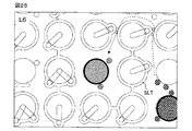
《マイクロコンピュータのメモリインタフェース回路配置》
図1には本発明に係るマイクロコンピュータにおけるメモリインタフェース形態が例示される。1はマイクロコンピュータ(MCU)であり、2,3はDDR2−SDRAMである。特に1Aはマイクロコンピュータチップ(MCU_CHP)を意味する。ここではマイクロコンピュータ1及びDDR2−SDRAM(以下単にSDRAMとも記す)2,3は各々パッケージされ、プリント配線基板(PCB)に実装される場合を想定する。SDRAM2,3はBGA(Ball Grid Array)パッケージを有し、その端子配列は前記非特許文献1にて規定される。例えば並列データ入出力ビット数が×16ビットの場合における端子配列は図2に示される。この端子配列に従えば、データ及びデータストローブ系信号端子群とコマンド及びアドレス系端子群CAPAが分離され、データ及びデータストローブ系信号端子群も上位バイトユニット端子群UBPAと下位バイトユニット端子群LBPAに分離される。それら端子群は、前記規格におけるA1番端子側の短辺を基点に、長辺に沿って、上位バイトユニット端子群UBPA、下位バイトユニット端子群LBPA、コマンド及びアドレス系端子群CAPAの順に配列される。図2において、DQ0〜DQ15がデータ入出力端子、LDQS,LDQSBはDQ0〜DQ7の下位バイトデータに対する差動のデータストローブ端子、UDQS、UDQSBはDQ8〜DQ15の上位バイトデータに対する差動のデータストローブ端子、A0〜A15がアドレス入力端子、BA0〜BA2がバンクアドレス入力端子である。RASB,CASB,WEBはコマンド入力端子、CSBはチップ選択端子、CK,CKBは差動のクロック入力端子、CKEはクロックイネーブル端子、LDMはDQ0〜DQ7の下位バイトデータに対するデータマスク端子、UDMはDQ8〜DQ15の上位バイトデータに対するデータマスク端子である。VDD,VDDQはメモリ電源端子、VSS、VSSQはグランド端子である。VDDQ、VSSQはDDR2−SDRAMのデータ入出力系及びデータストローブ信号の入出力系回路(外部出力及び外部入出力回路)の電源とグランドに専用化される。VDD、VSSはDDR2−SDRAMのその他の回路(コア回路)の電源とグランドの外部端子とされる。ここではVDDQとVDDの電圧レベルは例えば1.8Vで等しく、VSSQとVSSの電圧レベルも0Vで等しいものとする。VDDL,VSSDLは内部タイミングの生成に利用するDLL(Delay Locked Loop)回路に専用の電源及びグランド電圧とされる。VREFは参照電位の入力端子であり、SSTL(Stub Series Terminated Transceiver Logic)における外部インタフェース用の判定レベルが与えられる。NCは非接続端子である。
<Microcomputer memory interface circuit layout>
FIG. 1 illustrates a memory interface form in a microcomputer according to the present invention. 1 is a microcomputer (MCU), and 2 and 3 are DDR2-SDRAMs. In particular, 1A means a microcomputer chip (MCU_CHP). Here, it is assumed that the
図1における配列Aと配列Bの双方において、マイクロコンピュータチップ(半導体チップ)1Aは、その一つのコーナー部を基点とする両側の縁辺に沿ってSDRAM2,3のためのメモリインタフェース回路4,5が分割配置されている。分割配置する理由は次の通りである。即ち、SDRAMのデータ及びデータストローブ系インタフェースはデータ1バイトにつき更にこれに対応するデータストローブ信号の差動対とデータマスク信号の3ビットの合計11ビットのI/Oセルを必要とする。一つのI/Oセルのセル幅を約80μmとすると、1バイト分のインタフェース信号だけで少なくとも880μmの幅が必要になる。電源およびGNDセルが入ることを考慮して幅が約2倍になるとすると1760μmを費やす。4バイト分でも7040μmとなり、データ及びデータストローブ系だけで7mm以上の幅が必要になり、これを1辺に配置しようとすれば、1辺が7mm以下の正方形チップは採用することができない。また、長辺が7mm以上の長方形チップを採用してもよいが、そうすると、チップ上における回路位置と回路特性との相関が大きくなり、信頼性低下の虞が増すことになる。そこで、マイクロコンピュータチップ1Aやパッケージの小型化に資することができ、マイクロコンピュータチップの信頼性も損なわないようにするために、前述のメモリインタフェース回路4,5の分割配置を採用した。
In both the array A and the array B in FIG. 1, the microcomputer chip (semiconductor chip) 1A includes
図1において、マイクロコンピュータチップ1Aに対するSDRAM2,3の接続形態として、SDRAM2,3の短辺をマイクロコンピュータに対向させる形態(配置A)と、SDRAM2,3の長辺をマイクロコンピュータに対向させる形態(配置B)とが示される。BGAパッケージの端子ピッチが縦横同じであることに鑑みれば、長辺を対向させた方がマイクロコンピュータ1とSDRAM2,3とを接続する配線(PCB配線)の密度を低くするのが容易であるから、この点で配置Bが優れる。更に、SDRAM2,3の端子配列は、その長辺に沿って、上位バイトユニット端子群UBPAと下位バイトユニット端子群LBPAとが分離されていることを考慮すると、配置Bを採用する方が、バイトユニット単位毎にPCB配線を規則化することが容易になる。また、配置Bを採用することになれば、マイクロコンピュータチップ1Aにおけるメモリインタフェース回路4,5のデータ及びデータストローブ信号系回路についてもバイトユニット単位毎に規則化することができ回路設計の容易化にも資することができる。これらの点においても配置Bが優れる。更に、データ及びデータストローブ系信号端子群から分離されたコマンド及びアドレス系端子群CAPAをマイクロコンピュータ1のコーナー部寄りとすることによりそれら端子とマイクロコンピュータ1を接続する。PCB配線は、マイクロコンピュータ1から引出した信号配線が2つに分岐し、分岐後の2本の配線長が等しい配線トポロジとすることができる(以下本明細書では、信号配線が2つに分岐し、分岐後の左右の配線長が等しい配線トポロジを「T字型トポロジ」と記す)。この場合も配置Bの方がPCB配線長が短くなる。図1においてUBCLは上位バイトユニット系PCB配線、LBCLは下位バイトユニット系PCB配線、CACLはコマンド及びアドレス系PCB配線を意味する。
In FIG. 1, the
図3にはマイクロコンピュータ1のメモリインタフェース回路4,5におけるデータ系ユニットのインタフェース機能が例示される。マイクロコンピュータ1において分割された各々のメモリインタフェース回路4,5も、SDRAM2,3の長辺に沿ったコマンド及びアドレス系端子群CAPA、下位バイトユニット端子群LBPA、上位バイトユニット端子群UBPAの配置に対応して、コマンド及びアドレス系インタフェースユニットCAIF及びデータ系ユニットとして2個のデータ系単位ユニットを持つ。一方のデータ系単位ユニットは上位データ系インタフェースユニットUBIF、他方のデータ系単位ユニットは下位データ系インタフェースユニットLBIFである。コマンド及びアドレス系インタフェースユニットCAIFはコマンド及びアドレス系端子群CAPA等に接続されるアドレス出力及びコマンド入出力インタフェース回路を備える。各々のデータ系単位ユニットLBIF,UBIFはデータ入出力の単位をバイトとするものであり、回路構成それ自体は下位バイト対応であろうと上位バイト対応であろうと同じであり、データやストローブ信号の割り当てが相違されるだけである。JEDEC標準のDDR2−SDRAMの端子配列によれば、DDR2−SDRAMは、その長辺に沿ってデータ及びデータストローブ信号系の端子群UBPA,LBPAとコマンド及びアドレス系の端子群CAPAは分離配置され、特に、並列データ入出力ビット数を16ビット(×16ビット)とするインタフェース仕様に対しては上位バイトのデータ及びデータストローブ信号系の上位バイトユニット端子群UBPAと、下位バイトのデータ及びデータストローブ信号系の端子群LBPAとの配置も分離されている。この長辺をマイクロコンピュータ1のデータ系ユニットUBIF,LBIFに対向させたとき、バイトのデータ及びデータストローブ信号系の端子群UBPA,LBPAからデータ系ユニットUBIF,LBIFに向く配線経路を単純化することが可能になる。このことは、PCBにおける配線設計容易性や、モジュール基板(半導体パッケージ基板)上における配線設計容易性を保障することになる。
FIG. 3 illustrates the interface function of the data system unit in the
図3において各々のデータ系単位ユニットLBIF,UBIFは、マイクロコンピュータチップ1Aの一つのコーナー部側から順に、7個のデータ入出力回路10、データマスク信号回路11、反転データストローブ信号回路12、非反転データストローブ信号回路13、及び1個のデータ入出力回路14を有する。要するに、マイクロコンピュータチップにおけるパッド電極配置が上述の配置になると言うことである。
In FIG. 3, each of the data system unit units LBIF and UBIF includes seven data input /
図4には図3のデータ系単位ユニットLBIF,UBIFにおけるインタフェース機能の配置を採用する理由が示される。図4においてSDRAM2,3のボール電極(BALL)からPCBへの配線引出し経路が例示されているが、ここではボール間を通る配線を1本とし、PCB上では貫通スルーホール(THRH)を用いて配線層間の接続を行なうものとする。要するに、低コストのPCBを用いる場合を想定する。このときの引出し配線の信号配列は、SDRAM2の下位バイトのデータ及びデータストローブ信号系の端子群LBPAに対しては配列SGA1となり、上位バイトのデータ及びデータストローブ信号系の端子群UBPAに対しては配列SGA2となる。SDRAM3の下位バイトのデータ及びデータストローブ信号系の端子群LBPAに対しては配列SGA3となり、上位バイトのデータ及びデータストローブ信号系の端子群UBPAに対しては配列SGA4となる。前記信号配列SGA1,SGA2,SGA4は等しく、それらに対して信号配列SGA3はデータ1ビットの配列が相違されるだけである。そこで、図3で説明したデータ系単位ユニットLBIF,UBIFにおけるインタフェース機能の配置を信号配列SGA1,SGA2,SGA4と一致させる。要するに、マイクロコンピュータチップ1Aにおけるメモリインタフェース回路4,5のデータ及びデータストローブ信号系回路の構成をバイトユニット単位毎に同一として、その回路設計の容易化を優先させるようにする。高々1ビットのデータ端子配置をPCB配線に対して最適化するために一部の回路ユニットの構成を変更することを回避する。
FIG. 4 shows the reason why the arrangement of the interface functions in the data system unit LBIF, UBIF of FIG. 3 is adopted. In FIG. 4, the wiring lead-out path from the ball electrodes (BALL) of the
図5にはマイクロコンピュータ1のボール電極配置が例示される。実際にはボール電極は縦横方向に所定ピッチでマトリクス配置されているが、ここでは便宜上、個々のボール電極を正方形の枠として作図している。マイクロコンピュータのパッケージはBGA形態とされ、マイクロコンピュータチップのパッド電極はチップ表面のWPP配線(再配線層)を介して半田バンプ電極(図示せず)に接続され、半田バンプ電極はボール電極に接続される。ボール電極に対する端子機能の割り当てはDDR2−SDRAM2,3の端子及び引出し配線の配置(図4)とマイクロコンピュータチップにおけるパッド電極配置(図3、図4)との対応関係を極力維持できるようにすればよい。その一例が図5に例示される。
FIG. 5 illustrates the ball electrode arrangement of the
ボール電極に対する端子機能の割り当てに関しては差動端子の配列を考慮している。即ち、LDQSとLDQSBのペア、UDQSとUDQSBのペア、CKとCKBのペアは、ペア毎に、最外周より第1周目と第2周目の隣接するボール電極に割り当て、又は第3周目と第4周目の隣接するボール電極に割り当てて、差動端子を構成させる。ここではPCB上においてボール間を通る配線を1本とし、PCB上では貫通スルーホール(THRH)を用いて配線層間の接続を行なうものとする。そうすると、ボールグリッドアレイの最外周より第1周目のボール電極に接続する配線はそのまま外側に引き出され、第2周目のボール電極に接続する配線は第1周目のボール電極に接続する2本の配線の間を通って外側に引き出される。第3周目と第4周目のボール電極に各々接続する配線は第1周目と第2周目のボール電極とは異なる配線層を通って同様に外側に引き出される。このような一般的な配線構造への対応を考慮すると、差動端子を第1周目と第2周目に隣接配置し、又は第3周目と第4周目に隣接配置することにより、差動端子に接続する配線は同一配線層上で隣接して相対することができるから、PCB上においても同相ノイズ成分のキャンセル効果を維持させることが容易になる。なお、CKとCKBのペアはコーナーに配置されることが多く、他エリアほど配線が密ではない。よって、CKとCKLBのペアこの形態の限りではない。 Regarding the assignment of terminal functions to the ball electrodes, the arrangement of differential terminals is considered. That is, a pair of LDQS and LDQSB, a pair of UDQS and UDQSB, and a pair of CK and CKB are assigned to the adjacent ball electrodes on the first and second rounds from the outermost circumference, or on the third round. Are assigned to the adjacent ball electrodes on the fourth circumference to form differential terminals. Here, it is assumed that one wiring passes between the balls on the PCB, and the connection between the wiring layers is made using a through-through hole (THRH) on the PCB. Then, the wiring connected to the ball electrode on the first circumference is drawn out from the outermost periphery of the ball grid array as it is, and the wiring connected to the ball electrode on the second circumference is connected to the ball electrode on the first circumference. It is pulled out through the wiring of the book. The wirings connected to the third and fourth ball electrodes are similarly drawn out through different wiring layers from the first and second ball electrodes. Considering the correspondence to such a general wiring structure, by arranging the differential terminals adjacent to the first and second turns, or adjacent to the third and fourth turns, Since the wirings connected to the differential terminals can be adjacent to each other on the same wiring layer, it is easy to maintain the canceling effect of the common-mode noise component even on the PCB. Note that the pair of CK and CKB is often arranged at a corner, and the wiring is not as dense as other areas. Therefore, the pair of CK and CKLB is not limited to this form.
図6にはマイクロコンピュータとDDR2−SDRAMをPCBに実装したたきの縦断面図が例示される。ここでは6層のPCBを示すが、配線層数はこれに限定されない。17、18はマイクロコンピュータ1とDDR2−SDRAMを接続する表層配線を模式的に示す。19はマイクロコンピュータ1とDDR2−SDRAMを接続する内層配線を模式的に示す。
FIG. 6 illustrates a vertical cross-sectional view of a microcomputer and DDR2-SDRAM mounted on a PCB. Although six layers of PCB are shown here, the number of wiring layers is not limited to this.
図7にはメモリインタフェース回路のデータ系単位ユニットLBIF,UBIFの一例が示される。データ系単位ユニットLBIF,UBIFは、例えば出力バッファ20、入出力バッファ21、出力ラッチ22、入力データのサンプリング回路23、データストローブ信号に従って入力データのサンプリング信号を生成する位相シフト回路24、及びサンプリングデータの転送タイミングを調整するタイミング調整回路25を有する。データ系単位ユニットLBIF,UBIFはメモリコントローラ(MCNT)26に接続される。メモリコントローラ26は中央処理装置(CPU)27からのDDR2−SDSRAM2,3に対するメモリアクセス要求に応答して、DDR2−SDSRAM2,3のインタフェースプロトコルに従ったメモリアクセス制御を行う。このときデータ系単位ユニットLBIF,UBIFはメモリコントローラ26とDDR2−SDRAM2,3との間のインタフェースを行う。28はクロック発生回路(CPG)である。前記メモリコントローラの機能はバスステートコントローラで実現する場合もある。
FIG. 7 shows an example of the data system unit LBIF, UBIF of the memory interface circuit. The data system unit LBIF, UBIF includes, for example, an
以上の説明ではBGA形態のパッケージに半導体チップを封止したマイクロコンピュータについて説明したが、チップの半田バンプ電極における端子機能の配列はパッケージのボール電極における端子機の配列と基本的に同じである。したがって、マイクロコンピュータチップ1Aをそのままベアチップとして用いる用途においても、ボール電極の配置に関する技術的事項も含めて上記と同様の作用効果を得ることができる。
In the above description, a microcomputer in which a semiconductor chip is sealed in a BGA type package has been described. However, the arrangement of terminal functions on the solder bump electrodes of the chip is basically the same as the arrangement of terminal machines on the ball electrodes of the package. Therefore, even in the application in which the
《マルチチップモジュール》
図8には本発明に係る半導体装置の一例であるマルチチップモジュールの縦断面図が例示される。マルチチップモジュール31は、モジュール基板32の一面に、データ処理デバイスとして1個のマイクロコンピュータチップ(MCU_CHP)1Aと、複数個のメモリデバイスとして2個のDDR2−SDRAM2(3)とを有する。マイクロコンピュータチップ(MCU_CHP)1AとDDR2−SDRAM2(3)は、モジュール基板32との隙間がアンダーフィル樹脂(図示せず)で充填されている。このマルチチップモジュール31はシステム・イン・パッケージのマイコンモジュールとして位置付けられる。
《Multi-chip module》
FIG. 8 illustrates a longitudinal sectional view of a multichip module which is an example of a semiconductor device according to the present invention. The
マイクロコンピュータチップ1Aはベアチップであり、半田バンプ電極を下にして、モジュール基板32にフェースダウンで実装される。DDR2−SDRAM2(3)は非特許文献1のJEDEC標準を満足した図2の端子配置を備えたボールグリッドアレイのパッケージに封止されて構成される。
The
モジュール基板32はコア層34とその表裏に形成されたビルドアップ層35、36とを有し、多層配線の樹脂基板として構成される。コア層34は例えば0.8mm程度の厚みを有する。ビルドアップ層35は例えば30〜40μm程度の厚みを有し、コア層34の側より配線層L3、L2、L1が形成されている。ビルドアップ層36は例えば30〜40μm程度の厚みを有し、コア層34の側より配線層L4、L5、L6が形成されている。配線層L1、L2は、主にマイクロコンピュータチップ1Aのバンプ電極38と、DDR2−SDRAM2(3)のボール電極39とを接続するための配線の形成に利用される。配線層L3は主にグランドプレーン(グランドパターン)の形成に利用される。配線層L4は主に電源プレーンの形成に利用される。配線層L5、L6は、配線層L1〜L4に形成される信号配線、グランドプレーン及び電源プレーンをモジュール基板の外部接続端子であるモジュールボール電極40に接続するための配線の形成に利用される。図において41は代表的に示されたスルーホールでありコア層34を貫通する。42はビアであり、ビアホール若しくはスルーホールの内面に導電性メッキを施した導電部を総称し、その上下の配線層若しくは金属パターンを導通させる。
The
《アドレス・コマンド系のメモリインタフェース》
図9にはマルチチップモジュール31の平面なレイアウト構成が例示される。モジュール基板32上におけるマイクロコンピュータチップ1AとDDR2−SDRAM2,3との相対位置関係は図1の配置Bと同じである。図1の配置Bにおいて、PCBをモジュール基板32に代え、マイクロコンピュータ1をマイクロコンピュータチップ1Aに代えて考えればよい。端子配列は図1の配置Bと等価である。
《Address / Command Memory Interface》
FIG. 9 illustrates a planar layout configuration of the
マイクロコンピュータチップ1Aにおけるメモリインタフェース回路4,5の構成は図3等で説明したのと同じである。メモリインタフェース回路5の上位データ系インタフェースユニットUBIFとSDRAM2の上位バイトユニット端子群UBPAはモジュール基板32のデータ系配線UD1で接続される。メモリインタフェース回路5の下位データ系インタフェースユニットLBIFとSDRAM2の下位バイトユニット端子群LBPAはモジュール基板32のデータ系配線LD1で接続される。メモリインタフェース回路4の上位データ系インタフェースユニットUBIFとSDRAM3の上位バイトユニット端子群UBPAはモジュール基板32のデータ系配線UD0で接続される。メモリインタフェース回路4の下位データ系インタフェースユニットLBIFとSDRAM3の下位バイトユニット端子群LBPAはモジュール基板32のデータ系配線LD0で接続される。
The configuration of the
メモリインタフェース回路4,5のコマンド及びアドレス系インタフェースユニットCAIFを対応するSDRAM2,3のコマンド及びアドレス系端子群に接続するためのコマンド及びアドレス配線CAは、マイクロコンピュータチップ1Aの一つのコーナー部を基点に前記DDR2−SDRAM2,3の間の領域を通り、途中で分岐して各々の前記DDR2−SDRAM2,3の端子に至る経路を有する。T字形の配線トポロジにより、モジュール基板32上におけるコマンド及びアドレス系配線経路の等長化が容易になる。
The command and address wiring CA for connecting the command of the
CK0はマイクロコンピュータチップ1Aのメモリインタフェース回路4からSDRAM3のクロック端子CK,CKBに差動クロックを供給する差動クロック配線である。同じく、CK1はマイクロコンピュータチップ1Aのメモリインタフェース回路5からSDRAM2のクロック端子CK,CKBに差動クロックを供給する差動クロック配線である。前記差動クロック配線CK0,CK1は前記主なコマンド及びアドレス配線CAの経路に沿って配置される。クロック信号CLK0,CK1はコマンド及びアドレス信号の取り込みタイミングを規定するからタイミングの整合という点において両者を並走させること、即ち同じトポロジとするのが好都合である。コマンド及びアドレス系のタイミングマージンを大きくすることが容易になる。
CK0 is a differential clock wiring for supplying a differential clock from the
図10にはデータ系配線UD1、LD1に対する等長化経路の例が示される。図10より明らかなようにSDRAM2のバイトユニット端子群UBPAのボール電極は左右に離間しているから、同一バイト内のデータ及びデータストローブ端子に関し、最も大きな距離のある端子間の配線長に揃えることとし、端子間距離に比べてその配線長が長すぎる端子間配線につては、等長化のために同一配線の一部に折り返し経路を形成する。図10には代表的に折り返し経路FLa,FLbが示されている。折り返し経路によってデータ及びデータストローブ信号系配線の等長化が容易になる。図11に例示されるようにマイクロコンピュータチップ1AとSDRAM3との間についてもどうようである。図11には代表的に折り返し経路FLc,FLdが示されている。
FIG. 10 shows an example of equal length paths for the data system wires UD1 and LD1. As apparent from FIG. 10, since the ball electrodes of the byte unit terminal group UBPA of the
図12にはコマンド及びアドレス系配線CAa〜CAdに対する等長化経路の例が示される。T字形トポロジのコマンド及びアドレス系配線において、分岐点より後段には、L2配線の2本セット毎の間に距離DSTを取り、AR1、AR2の位置に代表されるように、信号毎にL1配線とL2配線との間のビア1個と配線1本を通すことができる余地を確保し、PNT1,PNT2に代表されるようにL2配線層の分岐位置を微調整可能にする。分基点以降において、等長化のために同じDDR2−SDRAMへの相互に異なる配線間で伝播方向が逆にされた逆方向経路を一部に有する。図12には代表的に逆方向経路RPa,RPbが示されている。逆方向経路RPa,RPbによってコマンド及びアドレス系配線の等長化が容易になる。 FIG. 12 shows an example of equal length paths for the command and address system wirings CAa to CAd. In T-shaped topology command and address system wiring, after the branch point, a distance DST is taken between every two sets of L2 wiring, and L1 wiring for each signal as represented by the positions of AR1 and AR2. And a space through which one via and one wiring between L2 wiring can be passed, and the branch position of the L2 wiring layer can be finely adjusted as represented by PNT1 and PNT2. After the split base point, in order to make the length equal, a part of the reverse direction path has a propagation direction reversed between different wirings to the same DDR2-SDRAM. FIG. 12 representatively shows reverse paths RPa and RPb. The reverse paths RPa and RPb facilitate the equalization of the command and address system wiring.
図13にはクロック系配線CK0,CK1に対する等長化経路の例が示される。前述の通りクロック系配線CK0,CK1はT形トポロジのコマンド及びアドレス系配線に沿うように配線される。更に、コマンド及びアドレス系配線の真ん中に配置する。これにより、コマンド及びアドレス系配線のマイクロコンピュータとSDRAM間の最長配線と最短配線との各々の差分をそれぞれ均等化し易くなる。これにより、コマンド及びアドレスに関するタイミングマージンの確保が容易になる。 FIG. 13 shows an example of equal length paths for the clock system wirings CK0 and CK1. As described above, the clock wirings CK0 and CK1 are wired so as to follow the command and address wiring of the T-type topology. Furthermore, it is arranged in the middle of the command and address system wiring. This makes it easy to equalize the differences between the longest wiring and the shortest wiring between the microcomputer of the command and address system wiring and the SDRAM. This facilitates securing a timing margin related to the command and address.
《差動信号用ボール電極の配置》
図14にはDDR2−SDRAM2,3に対するテスト専用端子の配置が例示される。モジュール基板32の裏面に配置されたボール電極40は外周縁に沿って7周配置された周回電極部分45と、中央部の9行9列でマトリクス配置された中央電極部分46とを有する。周回電極部分45と中央電極部分46の間には空白領域47が確保されている。マルチチップモジュール31には、DDR2−SDRAM2,3をマイクロコンピュータチップ1Aによるアクセス制御とは別に、外部よる単独でテスト可能にするテスト用のボール電極が配置される。テスト用のボール電極の領域は、DDR2−SDRAM2,3のボール電極39との対応が矢印で示されている。図より明らかなように、テスト用のボール電極は周回電極部分の内周寄りに配置されている。マルチチップモジュール31を搭載するマザーボード(プリント配線基板)上にマルチチップモジュール31を搭載するとき、マルチチップモジュール31の下側から側方に向けてPCB配線を引き出す場合、マルチチップモジュール31の周縁に近いほどマザーボード上における配引出しは容易である。したがって、テスト専用ボール電極の如くマザーボード上の配線に接続する必要のない端子は極力、モジュール基板の内側に集めた方が得策だからである。
<< Placement of differential signal ball electrode >>
FIG. 14 illustrates the arrangement of the test dedicated terminals for the DDR2-
ここで、前記差動クロック配線CK1は、SDRAM2のクロック端子CK,CKBの近傍に配置された差動終端抵抗接続用の一対のボール電極BCKa,BCKbを有する。前記ボール電極BCKa,BCKbは、相互に隣接され、且つ、他のモジュール端子が配置されていない領域に隣接し又はテスト専用モジュール端子に隣接して形成されている。SDRAM3のための差動クロック配線CK0についても同様に、差動終端抵抗接続用の一対のボール電極BCKc,BCKdを有する。前記ボール電極BCKc,BCKdも相互に隣接され、且つ、他のモジュール端子が配置されていない領域に隣接し又はテスト専用モジュール端子に隣接して形成されている。
Here, the differential clock wiring CK1 has a pair of ball electrodes BCKa and BCKb for connecting a differential termination resistor disposed in the vicinity of the clock terminals CK and CKB of the
マルチチップモジュール31が実装されるPCBにはテスト専用モジュール端子に接続されるべき配線は形成されていないから、差動終端抵抗接続用ボール電極BCKaとBCKb、BCKcとBCKdを、他のモジュール端子が配置されていない領域に隣接し又はテスト専用モジュール端子に隣接して形成することにより、当該差動終端抵抗接続用のボール電極BCKaとBCKb、BCKcとBCKdに各々直接終端抵抗を搭載することが容易になる。このことは分岐点から差動終端抵抗までの配線経路を極めて短く且つ等長化するのに好適である。この関係は、LDQSとLDQSB、UDQSとUDQSBのような差動データストローブ信号についても同様に適用すれば有効であるが、JEDEC標準によれば、それら差動データストローブ信号については、ODT(On-Die Termination)によるチップ内終端抵抗によって対策されることを期待することができるので、差動クロック配線と同様の考慮を払わなくても実質的な問題は少ないと考えられる。
Since the PCB on which the
図15にはSDRAM2のクロック端子CK,CKBの近傍に配置された差動終端抵抗接続用の一対のボール電極BCKa,BCKbと、差動データストローブ端子LDQS,LDQSBの近傍に配置された差動終端抵抗接続用の一対のボール電極BDQSa,BDQSbとの配置領域の詳細を例示する。差動終端抵抗接続用のボール電極BCKa,BCKbは周回電極部分45の内周縁に配置されていないが、図において左隣にはPCB配線引出し不用のボール電極を配置してあるから、終端抵抗の実装領域MAR1を確保することができる。また、差動終端抵抗接続用のボール電極BDQSa,BDQSbの双方は周回電極部分45の内周縁に配置されていないが、図において右隣にはPCB配線引出し不用のボール電極を配置し、左側には空白領域47はあるので、終端抵抗の実装領域MAR2を容易に確保することができる。
FIG. 15 shows a pair of ball electrodes BCKa and BCKb for connecting a differential termination resistor disposed in the vicinity of the clock terminals CK and CKB of the
《電源分離》
DDR2−SDRAM2,3の動作電源は、VDDQ,VSSQが外部出力及び外部入出力回路用(I/O用)の電源系端子セット、VDD,VSSがコア回路用の電源系端子セットである。マイクロコンピュータチップ1Aは、コア回路用と外部インタフェース回路用に別々の電源系端子セットを備える。更に、マイクロコンピュータチップ1Aは、SDRAM2,3にインタフェースされる前記インタフェース回路4,5の動作電源としてVCCddr、VSSddrの電源系端子セットを有する。電源端子VDD,VDDQ、VCCddrの電源電圧は例えば1.8Vである。グランド端子VSS、VSSQ、VSSddrのグランド電圧は0Vである。特に制限されないが、マイクロコンピュータチップ1Aのコア回路用電源セットは固有の電源系端子による1.0Vと0Vであり、その他の外部インタフェース回路用の電源セットはそれ固有の電源系端子による3.3Vと0Vである。
<Power supply isolation>
As for the operating power of the DDR2-
モジュール基板において、マイクロコンピュータチップ1AとDDR2−SDRAM2,3との間では動作電源経路が分離され、個別テストの便に供することができるようになっている。更に、DDR2−SDSRAMアクセスに際して電源系ノイズが回り込みことを防止する観点より、DDR2−SDRAM2,3のI/O用電源端子VDDQとコア回路用電源端子VDDとは相互に電気的に分離された固有の電源経路を経て接続された電源ボール電極が割り当てられる。VSS、VSSQ、VSSddrに接続するボール電極は電気的に分離されていない。ESD耐性の確保と電気的基準の安定化を確保するためである。
In the module substrate, the operating power supply path is separated between the
図16にはモジュール基板の電源用ボール電極の配置が例示される。Vdd−DRAMはSDRAM2,3の電源端子VDDに割り当てられた電源ボール電極、Vddq−DRAMはSDRAM2,3の電源端子VDDQに割り当てられた電源ボール電極、Vcc−DDRはマイクロコンピュータチップ1Aの電源端子VCCddrに割り当てられた電源ボール電極、Vssは、VSS,VSSQ,VSSddrに割り当てられたグランドボール電極である。
FIG. 16 illustrates the arrangement of the power supply ball electrodes on the module substrate. Vdd-DRAM is a power supply ball electrode assigned to the power supply terminal VDD of the
図17にはMCU−CHP1AからDDR−SDRAM2に出力される信号の変化に伴う電源系の帰還電流経路が模式的に示される。Vcc−DDRとVddq−DRAMとが分離されているとき、MCU−CHP1AとDDR2−SDRAM2との間で信号が充放電されると、その充放電電流のうち電源配線に流れる帰還電流の経路VDPS1とVDPS2はモジュール基板32上においてVddq−DRAMとVcc−DDRとによって分断され、マザーボード上の電源配線若しくは電源プレーンを介して帰還されなければならない。このことが電源系のインピーダンス増加を招くことになるが、これを極力抑制するために、Vcc−DDRとVddq−DRAMを直近に配置してある。これにより、50で示されるようにVcc−DDRとVddq−DRAMとを流れる逆方向の電流をカップリングさせて実効インダクタンスを減らすことができる。
FIG. 17 schematically shows a feedback current path of the power supply system accompanying a change in the signal output from the MCU-
《メモリコアへの給電ビア複数化》
図18には主な電源系に着目したときのマルチチップモジュール31の縦断面構造が例示される。DDR2−SDRAM2,3はI/O回路に比べてコア回路の消費電力の方が大きい。リフェレッシュ動作時の比較的大きな電力消費を考慮しなければならないからである。ここで、ビルドアップ層35、36に形成された1個のビア42Aの給電面積はコア層34に形成された1個のビア42Bの給電面積よりも小さい。このとき、Vdd−DRAMをVDDに接続する給電経路において前記コア層34の1個のビア42Bに対してビルドアップ層の各層に形成されるビア42Aの数は2個とされる。Vddq−DRAMをVDDQに接続する給電経路において前記コア層34の1個のビア42Bに対してビルドアップ層35,36の各層に形成されるビア42Aの数は1個とされる。メモリデバイスのコア回路による消費電力がI/O回路部分よりも大きくなることを考慮したとき、コア層のビアに比べて導電面積の小さなビルドアップ層のビアによる電流供給能力不足を生じないようにすることができる。
<Multiple power supply vias to memory core>
FIG. 18 illustrates a vertical cross-sectional structure of the
《グランドスリットによるノイズ対策》
図19にはグランド端子VSS,VSSQとグランドボール電極Vssを接続する経路の縦断面構造が例示される。前述のようにデバイス上で分離されているグランド端子VSS,VSSQはモジュール基板内では電気的に導通され、電気的に共通のグランドボール電極Vssに接続される。このとき、前記コア層とビルドアップ層は、グランド端子VSS,VSSQ及びグランドボール電極Vssに導通するグランドパターンGPTNを有し、面積を大きくして極力グランド電位の安定化を図ろうとしている。即ち、グランド端子VSS,VSSQ及びグランドボール電極Vssと、前記コア層及びビルドアップ層のグランドパターンGPTNとは電気的に一体化され、電源系のような分離は行なわれていないから、ESD(Electrostatic Discharge)耐性の低下、リターンパス経路の阻害に寄る電気的特性の劣化、グランドレベルのずれ等の問題を生じ難い。一方、グランドをDC的に全て共通化すると、VSSとVSSQのような異種グランド間でのノイズ回り込みの虞を生ずる。これに対し、前記グランドパターンGPTNは、デバイスグランド端子VSSに接続するパッド又はビアと、前記デバイスグランド端子VSSQに接続するパッド又はビアとを結ぶ線分の間にスリットSLTを有する。図20乃至図25には各配線層L1〜L6の状態が例示される。ここではL4配線層は基本的に電源プレーンに利用されるのでグランドパターンは存在していない。
<Measures against noise by ground slit>
FIG. 19 illustrates a vertical cross-sectional structure of a path connecting the ground terminals VSS and VSSQ and the ground ball electrode Vss. As described above, the ground terminals VSS and VSSQ separated on the device are electrically connected in the module substrate, and are electrically connected to the common ground ball electrode Vss. At this time, the core layer and the build-up layer have a ground pattern GPTN that is electrically connected to the ground terminals VSS and VSSQ and the ground ball electrode Vss, and the area is increased so as to stabilize the ground potential as much as possible. That is, since the ground terminals VSS, VSSQ and the ground ball electrode Vss are electrically integrated with the ground pattern GPTN of the core layer and the buildup layer and are not separated as in the power supply system, ESD (Electrostatic Discharge) It is difficult to cause problems such as a decrease in tolerance, deterioration of electrical characteristics due to the inhibition of the return path path, and ground level deviation. On the other hand, if all grounds are shared in terms of DC, there is a risk of noise sneaking between different grounds such as VSS and VSSQ. On the other hand, the ground pattern GPTN has a slit SLT between a line segment connecting a pad or via connected to the device ground terminal VSS and a pad or via connected to the device ground terminal VSSQ. 20 to 25 illustrate the states of the wiring layers L1 to L6. Here, since the L4 wiring layer is basically used as a power plane, there is no ground pattern.
前記スリットSLTがグランドパターンGPTN上で異種グランドのビアやパッド間の電気的導通経路を長くする。要するに、グランドパターンGPTNの平面上において異種グランド間の電気的導通経路が長くなる。これにより、実装基板上でグランドビア52Gと電源ビア52Vとの間に搭載されたパスコン53への縦方向の電気的導通経路にAC的なノイズが誘導され易くなるから、結果として、異種グランド間でのグランドノイズの回り込みを抑制若しくは緩和することができる。
The slit SLT lengthens the electrical conduction path between vias and pads of different grounds on the ground pattern GPTN. In short, the electrical conduction path between different kinds of grounds becomes long on the plane of the ground pattern GPTN. As a result, AC noise is easily induced in the vertical electrical conduction path to the
図26にはスリットSLTを形成しない場合の比較例が示される。VSSとVSSQの間ではL1層のグランパターンGPTNを介して異種電源の回り込みを生ずる。 FIG. 26 shows a comparative example in which the slit SLT is not formed. Between VSS and VSSQ, sneak currents of different types of power are generated via the L1 layer ground pattern GPTN.
図27には信号配線のガードに利用されるグランドプレーンの縁辺部分にスリットを適用した例が示される。例えばグランド端子VSSに接続するビア42G(VSS)グランドプレーンGPTNに着目すると、このグランドプレーンGPTNの縁辺部分55が信号配線SIGに対向するグランドガードとし利用されているとき、前記グランドプレーンの縁辺部分55とビア42G(VSS)との間に、スリットSLTを形成する。信号配線のガードに利用されるグランドプレーンの縁辺部分55には信号配線SIGに並行してリターン電流が流れるが、スリットSLTは前記信号配線SIGに隣接する縁辺部分55に対してリターンパスを確保するように作用し、且つ、リターンパスを流れる電流がノイズとしてデバイス2のグランド端子VSSに回り込むのを抑制することができる。スリットを形成する時に考慮すべきビアやパッドはVSSQに接続するものであってもよい。
FIG. 27 shows an example in which a slit is applied to an edge portion of a ground plane used for guarding signal wiring. For example, focusing on the via 42G (VSS) ground plane GPTN connected to the ground terminal VSS, when the
以上本発明者によってなされた発明を実施形態に基づいて具体的に説明したが、本発明はそれに限定されるものではなく、その要旨を逸脱しない範囲において種々変更可能であることは言うまでもない。 Although the invention made by the present inventor has been specifically described based on the embodiments, it is needless to say that the present invention is not limited thereto and can be variously modified without departing from the gist thereof.
例えば、DDR2−SDRAMの並列データ入出力ビット数は×8等であってもよい。マイクロコンピュータは汎用コントローラに限定されず、グラフィックコントローラ、符号化・複合処理を行なうコントローラなどであってよい。 For example, the number of parallel data input / output bits of DDR2-SDRAM may be x8 or the like. The microcomputer is not limited to a general-purpose controller, and may be a graphic controller, a controller that performs encoding / combination processing, or the like.
1 マイクロコンピュータ(MCU)
2,3 DDR2−SDRAM
4,5 メモリインタフェース回路
1A マイクロコンピュータチップ(MCU_CHP)
DQ0〜DQ15 データ入出力端子
LDQS,LDQSB 下位バイトデータに対する差動データストローブ端子
UDQS、UDQSB 上位バイトデータに対する差動データストローブ端子
A0〜A15 アドレス入力端子
BA0〜BA2 バンクアドレス入力端子
RASB、CASB、WEB コマンド入力端子
CSB チップ選択端子
CK,CKB 差動のクロック入力端子
LDM 下位バイトデータに対するデータマスク端子
UDM 上位バイトデータに対するデータマスク端子
VDD,VDDQ メモリ電源端子
VSS、VSSQ グランド端子
VCCddr MCUのメモリインタフェース回路用電源端子
UBCL 上位バイトユニット系PCB配線
LBCL 下位バイトユニット系PCB配線
CACL コマンド及びアドレス系PCB配線
CAPA コマンド及びアドレス系端子群
LBPA CAPA、下位バイトユニット端子群
UBPA 上位バイトユニット端子群
CAIF コマンド及びアドレス系インタフェースユニット
UBIF 上位データ系インタフェースユニット
LBIF 下位データ系インタフェースユニット
10 データ入出力回路
11 データマスク信号回路
12 反転データストローブ信号回路
13 非反転データストローブ信号回路
14 データ入出力回路14
20 入出力バッファ
21 出力バッファ
22 出力ラッチ
26 メモリコントローラ(MCNT)26
27 中央処理装置(CPU)
32 モジュール基板
34 コア層
35,36 ビルドアップ層
38 マイクロコンピュータチップ1Aのバンプ電極
39 DDR2−SDRAM2(3)のボール電極
40 モジュールボール電極
41 スルーホール
42 ビア
SLT スリット
GPTN グランドプレーン
55 グランドプレーンのガード用縁辺部分
Vcc DDR MCUのメモリインタフェース回路電源用モジュール端子
Vddq−DRAM DDR2−SDRAMのI/O電源用モジュール端子
Vdd−DRAM DDR2−SDRAMのコア電源用モジュール端子
1 Microcomputer (MCU)
2,3 DDR2-SDRAM
4,5
DQ0 to DQ15 Data input / output terminals LDQS, LDQSB Differential data strobe terminals for lower byte data UDQS, UDQSB Differential data strobe terminals for upper byte data A0 to A15 Address input terminals BA0 to BA2 Bank address input terminals RASB, CASB, WEB command Input terminal CSB Chip selection terminal CK, CKB Differential clock input terminal LDM Data mask terminal for lower byte data UDM Data mask terminal for upper byte data VDD, VDDQ Memory power supply terminal VSS, VSSQ Ground terminal VCCddr Power supply for memory interface circuit of MCU Terminal UBCL Upper byte unit system PCB wiring LBCL Lower byte unit system PCB wiring CACL command and address system PCB wiring Line CAPA Command and address system terminal group LBPA CAPA, Lower byte unit terminal group UBPA Upper byte unit terminal group CAIF Command and address system interface unit UBIF Upper data system interface unit LBIF Lower data
20 I /
27 Central processing unit (CPU)
32
Claims (5)
前記データ処理デバイスは、上面および前記上面とは反対側の下面を有するパッケージと、第1反転データストローブ信号回路および第1非反転データストローブ信号回路を有し、かつ前記パッケージの前記上面に搭載されたマイクロコンピュータチップと、前記パッケージの前記下面に形成された複数のボール電極とを含み、
前記パッケージの平面形状は、第1辺を有する四角形からなり、
前記マイクロコンピュータチップの平面形状は、第2辺を有する四角形からなり、
前記マイクロコンピュータチップは、平面視において、前記マイクロコンピュータチップの前記第2辺が前記パッケージの前記第1辺と並ぶように、前記パッケージの前記上面に搭載され、
前記第1反転データストローブ信号回路および前記第1非反転データストローブ信号回路は、前記マイクロコンピュータチップの前記第2辺に沿って隣接配置されており、
前記複数のボール電極は、平面視において、前記第1辺に沿って、かつ、複数列に亘って配置されており、
前記複数のボール電極のうち、前記パッケージに形成された第1配線を介して前記マイクロコンピュータチップの前記第1非反転データストローブ信号回路と電気的に接続され、かつ、前記第1メモリデバイスの前記第1非反転データストローブ信号回路用端子と電気的に接続される第1非反転データストローブ信号回路用ボール電極は、前記複数のボール電極のうち、前記パッケージに形成された第2配線を介して前記マイクロコンピュータチップの前記第1反転データストローブ信号回路と電気的に接続され、かつ、前記第1メモリデバイスの前記第1反転データストローブ信号回路用端子と電気的に接続される第1反転データストローブ信号回路用ボール電極と、前記下面における前記第1辺と交差する方向に沿って隣接配置されており、
前記第1反転データストローブ信号回路用ボール電極および前記第1非反転データストローブ信号回路用ボール電極は、前記複数のボール電極のうちの第1周目および第2周目、または第3周目および第4周目に、それぞれ割り当てられていることを特徴とするデータ処理デバイス。 A data processing device mounted on a printed wiring board on which a first memory device having a first inverted data strobe signal circuit terminal and a first non-inverted data strobe signal circuit terminal is mounted,
The data processing device includes a package having an upper surface and a lower surface opposite to the upper surface, a first inverted data strobe signal circuit and a first non-inverted data strobe signal circuit, and is mounted on the upper surface of the package A microcomputer chip, and a plurality of ball electrodes formed on the lower surface of the package ,
The planar shape of the package is a quadrangle having a first side,
The planar shape of the microcomputer chip is a quadrangle having a second side,
The microcomputer chip is mounted on the upper surface of the package so that the second side of the microcomputer chip is aligned with the first side of the package in plan view,
The first inverted data strobe signal circuit and the first non-inverted data strobe signal circuit are adjacently disposed along the second side of the microcomputer chip,
The plurality of ball electrodes are arranged along the first side and in a plurality of rows in plan view,
Of the plurality of ball electrodes, the first non-inverted data strobe signal circuit of the microcomputer chip is electrically connected through a first wiring formed in the package , and the first memory device has the first memory device. The first non-inverted data strobe signal circuit ball electrode electrically connected to the first non-inverted data strobe signal circuit terminal is connected to the plurality of ball electrodes via a second wiring formed in the package. A first inverted data strobe electrically connected to the first inverted data strobe signal circuit of the microcomputer chip and electrically connected to the first inverted data strobe signal circuit terminal of the first memory device. and the ball electrode signal circuit, it is adjacently disposed along a direction intersecting with the first side of the lower surface ,
The ball electrode for the first inverted data strobe signal circuit and the ball electrode for the first non-inverted data strobe signal circuit include a first circumference and a second circumference, or a third circumference of the plurality of ball electrodes, and A data processing device, which is assigned in the fourth round .
前記マイクロコンピュータチップは、上位バイト用の前記第1反転データストローブ信号回路と、上位バイト用の前記第1非反転データストローブ信号回路と、下位バイト用の第2反転データストローブ信号回路と、下位バイト用の第2非反転データストローブ信号回路とを有しており、
前記複数のボール電極のうち、前記パッケージに形成された第3配線を介して前記マイクロコンピュータチップの前記第2非反転データストローブ信号回路と電気的に接続され、かつ、前記第1メモリデバイスの前記第2非反転データストローブ信号回路用端子と電気的に接続される第2非反転データストローブ信号回路用ボール電極は、前記複数のボール電極のうち、前記パッケージに形成された第4配線を介して前記マイクロコンピュータチップの前記第2反転データストローブ信号回路と電気的に接続され、かつ、前記第1メモリデバイスの前記第2反転データストローブ信号回路用端子と電気的に接続される第2反転データストローブ信号回路用ボール電極と隣接配置されていることを特徴とする請求項1記載のデータ処理デバイス。 The first memory device includes a terminal for the first inverted data strobe signal circuit for the upper byte, a terminal for the first non-inverted data strobe signal circuit for the upper byte, and a second inverted data strobe signal for the lower byte. A circuit terminal and a second non-inverted data strobe signal circuit terminal for the lower byte,
The microcomputer chip includes the first inverted data strobe signal circuit for upper bytes, the first non-inverted data strobe signal circuit for upper bytes, a second inverted data strobe signal circuit for lower bytes, and a lower byte A second non-inverted data strobe signal circuit for
Among the plurality of ball electrodes, the second non-inverted data strobe signal circuit of the microcomputer chip is electrically connected through a third wiring formed in the package , and the first memory device has the first memory device. The second non-inverted data strobe signal circuit ball electrode electrically connected to the second non-inverted data strobe signal circuit terminal is connected to the ball electrode for the second non-inverted data strobe signal circuit via a fourth wiring formed in the package. A second inverted data strobe electrically connected to the second inverted data strobe signal circuit of the microcomputer chip and electrically connected to the second inverted data strobe signal circuit terminal of the first memory device. 2. The data processing device according to claim 1, wherein the data processing device is disposed adjacent to the ball electrode for the signal circuit.
第1非反転データストローブ信号回路用ボール電極は、前記プリント配線基板の前記第1配線層に形成され、かつ前記第1差動信号配線の隣に形成された第2差動信号配線を介して前記第1非反転データストローブ信号回路用端子と電気的に接続され、
第2反転データストローブ信号回路用ボール電極は、前記プリント配線基板の前記第1配線層に形成された第3差動信号配線を介して前記第2反転データストローブ信号回路用端子と電気的に接続され、
第2非反転データストローブ信号回路用ボール電極は、前記プリント配線基板の前記第1配線層に形成され、かつ前記第3差動信号配線の隣に形成された第4差動信号配線を介して前記第2非反転データストローブ信号回路用端子と電気的に接続されることを特徴とする請求項3記載のデータ処理デバイス。 The ball electrode for the first inverted data strobe signal circuit is electrically connected to the terminal for the first inverted data strobe signal circuit via the first differential signal wiring formed in the first wiring layer of the printed wiring board. ,
A ball electrode for the first non-inverted data strobe signal circuit is formed on the first wiring layer of the printed wiring board and via a second differential signal wiring formed adjacent to the first differential signal wiring. Electrically connected to the first non-inverted data strobe signal circuit terminal;
The second inverted data strobe signal circuit ball electrode is electrically connected to the second inverted data strobe signal circuit terminal through a third differential signal wiring formed in the first wiring layer of the printed wiring board. And
The second non-inverted data strobe signal circuit ball electrode is formed on the first wiring layer of the printed wiring board and via a fourth differential signal wiring formed adjacent to the third differential signal wiring. 4. The data processing device according to claim 3, wherein the data processing device is electrically connected to the second non-inverted data strobe signal circuit terminal.
前記マイクロコンピュータチップは、さらに、上位バイト用の第3反転データストローブ信号回路と、上位バイト用の第3非反転データストローブ信号回路と、下位バイト用の第4反転データストローブ信号回路と、下位バイト用の第4非反転データストローブ信号回路とを有しており、
前記複数のボール電極のうち、前記パッケージに形成された第5配線を介して前記マイクロコンピュータチップの前記第3非反転データストローブ信号回路と電気的に接続され、かつ、前記第2メモリデバイスの前記第3非反転データストローブ信号回路用端子と電気的に接続される第3非反転データストローブ信号回路用ボール電極は、前記複数のボール電極のうち、前記パッケージに形成された第6配線を介して前記マイクロコンピュータチップの前記第3反転データストローブ信号回路と電気的に接続され、かつ、前記第2メモリデバイスの前記第3反転データストローブ信号回路用端子と電気的に接続される第3反転データストローブ信号回路用ボール電極と隣接配置されており、
前記複数のボール電極のうちの前記第4非反転データストローブ信号回路と電気的に接続され、かつ、前記第2メモリデバイスの前記第4非反転データストローブ信号回路用端子と電気的に接続される第4非反転データストローブ信号回路用ボール電極は、前記複数のボール電極のうちの前記第4反転データストローブ信号回路と電気的に接続され、かつ、前記第2メモリデバイスの前記第4反転データストローブ信号回路用端子と電気的に接続される第4反転データストローブ信号回路用ボール電極と隣接配置されていることを特徴とする請求項4記載のデータ処理デバイス。 The printed wiring board further includes a third inverted data strobe signal circuit terminal for the upper byte, a third non-inverted data strobe signal circuit terminal for the upper byte, and a fourth inverted data strobe signal for the lower byte. A second memory device having a circuit terminal and a fourth non-inverted data strobe signal circuit terminal for a lower byte is mounted;
The microcomputer chip further includes a third inverted data strobe signal circuit for an upper byte, a third non-inverted data strobe signal circuit for an upper byte, a fourth inverted data strobe signal circuit for a lower byte, and a lower byte And a fourth non-inverted data strobe signal circuit for
Of the plurality of ball electrodes, the third non-inverted data strobe signal circuit of the microcomputer chip is electrically connected via a fifth wiring formed in the package , and the second memory device The third non-inverted data strobe signal circuit ball electrode electrically connected to the third non-inverted data strobe signal circuit terminal is connected to the plurality of ball electrodes via a sixth wiring formed in the package. A third inverted data strobe electrically connected to the third inverted data strobe signal circuit of the microcomputer chip and electrically connected to the third inverted data strobe signal circuit terminal of the second memory device. It is placed adjacent to the ball electrode for signal circuit,
Of the plurality of ball electrodes, electrically connected to the fourth non-inverted data strobe signal circuit and electrically connected to the fourth non-inverted data strobe signal circuit terminal of the second memory device. A ball electrode for a fourth non-inverted data strobe signal circuit is electrically connected to the fourth inverted data strobe signal circuit of the plurality of ball electrodes, and the fourth inverted data strobe of the second memory device. 5. The data processing device according to claim 4, wherein the data processing device is disposed adjacent to a ball electrode for a fourth inverted data strobe signal circuit electrically connected to a signal circuit terminal.
Priority Applications (9)
| Application Number | Priority Date | Filing Date | Title |
|---|---|---|---|
| JP2006033513A JP4662474B2 (en) | 2006-02-10 | 2006-02-10 | Data processing device |
| US11/616,966 US8091061B2 (en) | 2006-02-10 | 2006-12-28 | Microcomputer having memory interface circuits and memory devices on a module board |
| US13/310,217 US8386992B2 (en) | 2006-02-10 | 2011-12-02 | Data processing device |
| US13/748,167 US8694949B2 (en) | 2006-02-10 | 2013-01-23 | Data processing device |
| US14/182,821 US8898613B2 (en) | 2006-02-10 | 2014-02-18 | Data processing device |
| US14/519,967 US9530457B2 (en) | 2006-02-10 | 2014-10-21 | Data processing device |
| US15/351,580 US9792959B2 (en) | 2006-02-10 | 2016-11-15 | Data processing device |
| US15/351,600 US10020028B2 (en) | 2006-02-10 | 2016-11-15 | Data processing device |
| US16/010,770 US10726878B2 (en) | 2006-02-10 | 2018-06-18 | Data processing device |
Applications Claiming Priority (1)
| Application Number | Priority Date | Filing Date | Title |
|---|---|---|---|
| JP2006033513A JP4662474B2 (en) | 2006-02-10 | 2006-02-10 | Data processing device |
Related Child Applications (1)
| Application Number | Title | Priority Date | Filing Date |
|---|---|---|---|
| JP2010271403A Division JP4979097B2 (en) | 2010-12-06 | 2010-12-06 | Multi-chip module |
Publications (3)
| Publication Number | Publication Date |
|---|---|
| JP2007213375A JP2007213375A (en) | 2007-08-23 |
| JP2007213375A5 JP2007213375A5 (en) | 2010-03-04 |
| JP4662474B2 true JP4662474B2 (en) | 2011-03-30 |
Family
ID=38370125
Family Applications (1)
| Application Number | Title | Priority Date | Filing Date |
|---|---|---|---|
| JP2006033513A Active JP4662474B2 (en) | 2006-02-10 | 2006-02-10 | Data processing device |
Country Status (2)
| Country | Link |
|---|---|
| US (8) | US8091061B2 (en) |
| JP (1) | JP4662474B2 (en) |
Families Citing this family (25)
| Publication number | Priority date | Publication date | Assignee | Title |
|---|---|---|---|---|
| JP4662474B2 (en) * | 2006-02-10 | 2011-03-30 | ルネサスエレクトロニクス株式会社 | Data processing device |
| CN101636702B (en) * | 2006-09-25 | 2014-03-05 | 弗莱克斯电子有限责任公司 | Bi-directional regulator |
| JP5288783B2 (en) * | 2007-12-12 | 2013-09-11 | キヤノン株式会社 | Bonding pad arrangement method, semiconductor chip and system |
| JP5197080B2 (en) * | 2008-03-19 | 2013-05-15 | ルネサスエレクトロニクス株式会社 | Semiconductor device and data processor |
| US7987581B2 (en) | 2008-05-28 | 2011-08-02 | Flextronics Ap, Llc | High power manufacturing friendly transformer |
| US8586873B2 (en) * | 2010-02-23 | 2013-11-19 | Flextronics Ap, Llc | Test point design for a high speed bus |
| DE112013003806T5 (en) * | 2012-08-01 | 2015-04-23 | Samtec, Inc. | Multilayer transmission lines |
| KR102032887B1 (en) * | 2012-12-10 | 2019-10-16 | 삼성전자 주식회사 | Semiconductor package and method for routing the package |
| CN104636229A (en) * | 2013-11-13 | 2015-05-20 | 华为技术有限公司 | Method and system for adjusting line sequence of DDR |
| JP2015099890A (en) * | 2013-11-20 | 2015-05-28 | 株式会社東芝 | Semiconductor device and semiconductor package |
| JP2015111360A (en) | 2013-12-06 | 2015-06-18 | ソニー株式会社 | Semiconductor module |
| WO2016046987A1 (en) | 2014-09-26 | 2016-03-31 | ルネサスエレクトロニクス株式会社 | Electronic device and semiconductor device |
| US10043755B2 (en) | 2015-06-26 | 2018-08-07 | Renesas Electronics Corporation | Electronic device |
| JP6543129B2 (en) | 2015-07-29 | 2019-07-10 | ルネサスエレクトロニクス株式会社 | Electronic device |
| JP6443556B2 (en) | 2015-08-31 | 2018-12-26 | アイシン・エィ・ダブリュ株式会社 | Semiconductor device and semiconductor module |
| JP6669547B2 (en) * | 2016-03-23 | 2020-03-18 | 京セラ株式会社 | Wiring board |
| KR102509048B1 (en) * | 2016-04-26 | 2023-03-10 | 에스케이하이닉스 주식회사 | Semiconductor package |
| US10973116B2 (en) * | 2016-09-30 | 2021-04-06 | Intel Corporation | 3D high-inductive ground plane for crosstalk reduction |
| CN106375525A (en) * | 2016-11-30 | 2017-02-01 | 深圳天珑无线科技有限公司 | Anti-jamming circuit |
| KR102371893B1 (en) | 2017-05-18 | 2022-03-08 | 삼성전자주식회사 | Semiconductor memory chip, semiconductor memory package, and electronic system using the same |
| JP7279464B2 (en) | 2019-03-28 | 2023-05-23 | 株式会社アイシン | Electronic substrate |
| CN113906830B (en) * | 2019-06-11 | 2024-04-12 | 华为技术有限公司 | Circuit board and electronic equipment |
| CN111182722B (en) * | 2020-02-26 | 2021-01-29 | 王致刚 | MCU application circuit board of modularization concatenation |
| JP2022071887A (en) | 2020-10-29 | 2022-05-17 | ルネサスエレクトロニクス株式会社 | Electronic device and semiconductor device |
| CN113191110B (en) * | 2021-05-07 | 2023-08-11 | 瓴盛科技有限公司 | DDR4 address control line mapping and Ball arrangement method for T-shaped topological structure |
Citations (7)
| Publication number | Priority date | Publication date | Assignee | Title |
|---|---|---|---|---|
| JPH1167970A (en) * | 1997-08-25 | 1999-03-09 | Fujitsu Ltd | Wiring structure of lsi package |
| JP2000174505A (en) * | 1998-12-08 | 2000-06-23 | Kanji Otsuka | Electronic device |
| JP2001094032A (en) * | 1999-09-21 | 2001-04-06 | Matsushita Electronics Industry Corp | Semiconductor device |
| JP2004030641A (en) * | 2002-05-30 | 2004-01-29 | Hewlett-Packard Development Co Lp | Data bus having individually aligned line impedance and method for aligning line impedance |
| JP2005032417A (en) * | 2003-07-04 | 2005-02-03 | Samsung Electronics Co Ltd | Memory system and method capable of selectively operating in both dual data strobe mode and single data strobe mode having inversion |
| WO2005091367A1 (en) * | 2004-03-19 | 2005-09-29 | Renesas Technology Corp. | Electronic circuit, semiconductor device, and mounting board |
| JP2005340247A (en) * | 2004-05-24 | 2005-12-08 | Renesas Technology Corp | Semiconductor device |
Family Cites Families (24)
| Publication number | Priority date | Publication date | Assignee | Title |
|---|---|---|---|---|
| EP0597601A1 (en) * | 1992-11-13 | 1994-05-18 | National Semiconductor Corporation | Reflexively sizing memory bus interface |
| US5867726A (en) * | 1995-05-02 | 1999-02-02 | Hitachi, Ltd. | Microcomputer |
| JP3746161B2 (en) * | 1998-11-19 | 2006-02-15 | 富士通株式会社 | Semiconductor device |
| JP2000332369A (en) * | 1999-05-25 | 2000-11-30 | Mitsui Mining & Smelting Co Ltd | Printed-circuit board and its manufacture |
| JP2001015704A (en) * | 1999-06-29 | 2001-01-19 | Hitachi Ltd | Semiconductor integrated circuit |
| US6484290B1 (en) * | 1999-11-03 | 2002-11-19 | Feiya Technology Corp. | IC package similar IDE interface solid state disk module and optimized pin design |
| JP2001217508A (en) * | 2000-01-31 | 2001-08-10 | Toshiba Corp | Printed board |
| JP2002041452A (en) * | 2000-07-27 | 2002-02-08 | Hitachi Ltd | Microprocessor, semiconductor module and data processing system |
| US6806733B1 (en) | 2001-08-29 | 2004-10-19 | Altera Corporation | Multiple data rate interface architecture |
| WO2003046725A1 (en) * | 2001-11-30 | 2003-06-05 | Fujitsu Ten Limited | Microcomputer logic developing apparatus |
| US6807650B2 (en) * | 2002-06-03 | 2004-10-19 | International Business Machines Corporation | DDR-II driver impedance adjustment control algorithm and interface circuits |
| JP2004030438A (en) * | 2002-06-27 | 2004-01-29 | Renesas Technology Corp | Microcomputer |
| US20050050375A1 (en) | 2003-08-29 | 2005-03-03 | Mark Novak | Memory interface system and method |
| JP3739375B2 (en) * | 2003-11-28 | 2006-01-25 | 沖電気工業株式会社 | Semiconductor device and manufacturing method thereof |
| JP4489485B2 (en) * | 2004-03-31 | 2010-06-23 | 株式会社ルネサステクノロジ | Semiconductor device |
| EP1805627B1 (en) * | 2004-10-15 | 2011-02-16 | Sony Computer Entertainment Inc. | Methods and apparatus for supporting multiple configurations in a multi-processor system |
| US7380052B2 (en) * | 2004-11-18 | 2008-05-27 | International Business Machines Corporation | Reuse of functional data buffers for pattern buffers in XDR DRAM |
| US20060149923A1 (en) * | 2004-12-08 | 2006-07-06 | Staktek Group L.P. | Microprocessor optimized for algorithmic processing |
| US20060136658A1 (en) * | 2004-12-16 | 2006-06-22 | Simpletech, Inc. | DDR2 SDRAM memory module |
| JP4662474B2 (en) * | 2006-02-10 | 2011-03-30 | ルネサスエレクトロニクス株式会社 | Data processing device |
| JP2008299476A (en) * | 2007-05-30 | 2008-12-11 | Fujitsu Microelectronics Ltd | Semiconductor integrated circuit |
| WO2011016157A1 (en) * | 2009-08-07 | 2011-02-10 | パナソニック株式会社 | Semiconductor device and electronic device |
| US9412423B2 (en) * | 2012-03-15 | 2016-08-09 | Samsung Electronics Co., Ltd. | Memory modules including plural memory devices arranged in rows and module resistor units |
| US9042188B2 (en) * | 2013-04-01 | 2015-05-26 | Arm Limited | Memory controller and method of calibrating a memory controller |
-
2006
- 2006-02-10 JP JP2006033513A patent/JP4662474B2/en active Active
- 2006-12-28 US US11/616,966 patent/US8091061B2/en active Active
-
2011
- 2011-12-02 US US13/310,217 patent/US8386992B2/en active Active
-
2013
- 2013-01-23 US US13/748,167 patent/US8694949B2/en active Active
-
2014
- 2014-02-18 US US14/182,821 patent/US8898613B2/en active Active
- 2014-10-21 US US14/519,967 patent/US9530457B2/en active Active
-
2016
- 2016-11-15 US US15/351,580 patent/US9792959B2/en active Active
- 2016-11-15 US US15/351,600 patent/US10020028B2/en active Active
-
2018
- 2018-06-18 US US16/010,770 patent/US10726878B2/en active Active
Patent Citations (7)
| Publication number | Priority date | Publication date | Assignee | Title |
|---|---|---|---|---|
| JPH1167970A (en) * | 1997-08-25 | 1999-03-09 | Fujitsu Ltd | Wiring structure of lsi package |
| JP2000174505A (en) * | 1998-12-08 | 2000-06-23 | Kanji Otsuka | Electronic device |
| JP2001094032A (en) * | 1999-09-21 | 2001-04-06 | Matsushita Electronics Industry Corp | Semiconductor device |
| JP2004030641A (en) * | 2002-05-30 | 2004-01-29 | Hewlett-Packard Development Co Lp | Data bus having individually aligned line impedance and method for aligning line impedance |
| JP2005032417A (en) * | 2003-07-04 | 2005-02-03 | Samsung Electronics Co Ltd | Memory system and method capable of selectively operating in both dual data strobe mode and single data strobe mode having inversion |
| WO2005091367A1 (en) * | 2004-03-19 | 2005-09-29 | Renesas Technology Corp. | Electronic circuit, semiconductor device, and mounting board |
| JP2005340247A (en) * | 2004-05-24 | 2005-12-08 | Renesas Technology Corp | Semiconductor device |
Also Published As
| Publication number | Publication date |
|---|---|
| JP2007213375A (en) | 2007-08-23 |
| US10726878B2 (en) | 2020-07-28 |
| US20180301172A1 (en) | 2018-10-18 |
| US20140160826A1 (en) | 2014-06-12 |
| US20170062020A1 (en) | 2017-03-02 |
| US8898613B2 (en) | 2014-11-25 |
| US9530457B2 (en) | 2016-12-27 |
| US10020028B2 (en) | 2018-07-10 |
| US8694949B2 (en) | 2014-04-08 |
| US20170062021A1 (en) | 2017-03-02 |
| US9792959B2 (en) | 2017-10-17 |
| US20120079238A1 (en) | 2012-03-29 |
| US20150036406A1 (en) | 2015-02-05 |
| US8386992B2 (en) | 2013-02-26 |
| US8091061B2 (en) | 2012-01-03 |
| US20070192559A1 (en) | 2007-08-16 |
| US20130128647A1 (en) | 2013-05-23 |
Similar Documents
| Publication | Publication Date | Title |
|---|---|---|
| JP4662474B2 (en) | Data processing device | |
| JP4979097B2 (en) | Multi-chip module | |
| US7745915B2 (en) | Semiconductor device | |
| JP4387403B2 (en) | Electronic circuit | |
| JP6200236B2 (en) | Electronic equipment | |
| JP5473317B2 (en) | Memory module and layout method thereof | |
| JP2008251917A (en) | Semiconductor device | |
| JP5574539B2 (en) | Semiconductor device and electronic device | |
| JP2012235048A (en) | Semiconductor device | |
| CN106409332A (en) | Electronic device | |
| JP4812107B2 (en) | Semiconductor device | |
| JP4674852B2 (en) | Semiconductor device | |
| JP2008004579A (en) | Semiconductor device | |
| US9226398B1 (en) | Printed circuit board and package substrate having additional conductive pathway space | |
| JP2010123203A (en) | Semiconductor device and module device | |
| Sun et al. | High-speed DIMM-in-a-Package (DIAP) memory module |
Legal Events
| Date | Code | Title | Description |
|---|---|---|---|
| A621 | Written request for application examination |
Free format text: JAPANESE INTERMEDIATE CODE: A621 Effective date: 20090202 |
|
| A521 | Written amendment |
Free format text: JAPANESE INTERMEDIATE CODE: A523 Effective date: 20100119 |
|
| A711 | Notification of change in applicant |
Free format text: JAPANESE INTERMEDIATE CODE: A712 Effective date: 20100507 |
|
| A131 | Notification of reasons for refusal |
Free format text: JAPANESE INTERMEDIATE CODE: A131 Effective date: 20101005 |
|
| A521 | Written amendment |
Free format text: JAPANESE INTERMEDIATE CODE: A523 Effective date: 20101206 |
|
| TRDD | Decision of grant or rejection written | ||
| A01 | Written decision to grant a patent or to grant a registration (utility model) |
Free format text: JAPANESE INTERMEDIATE CODE: A01 Effective date: 20101228 |
|
| A01 | Written decision to grant a patent or to grant a registration (utility model) |
Free format text: JAPANESE INTERMEDIATE CODE: A01 |
|
| A61 | First payment of annual fees (during grant procedure) |
Free format text: JAPANESE INTERMEDIATE CODE: A61 Effective date: 20101228 |
|
| R150 | Certificate of patent or registration of utility model |
Ref document number: 4662474 Country of ref document: JP Free format text: JAPANESE INTERMEDIATE CODE: R150 Free format text: JAPANESE INTERMEDIATE CODE: R150 |
|
| FPAY | Renewal fee payment (event date is renewal date of database) |
Free format text: PAYMENT UNTIL: 20140114 Year of fee payment: 3 |
|
| S531 | Written request for registration of change of domicile |
Free format text: JAPANESE INTERMEDIATE CODE: R313531 |
|
| R350 | Written notification of registration of transfer |
Free format text: JAPANESE INTERMEDIATE CODE: R350 |