JP4659472B2 - Capacitor device, fixing device, and image forming apparatus - Google Patents
Capacitor device, fixing device, and image forming apparatus Download PDFInfo
- Publication number
- JP4659472B2 JP4659472B2 JP2005026574A JP2005026574A JP4659472B2 JP 4659472 B2 JP4659472 B2 JP 4659472B2 JP 2005026574 A JP2005026574 A JP 2005026574A JP 2005026574 A JP2005026574 A JP 2005026574A JP 4659472 B2 JP4659472 B2 JP 4659472B2
- Authority
- JP
- Japan
- Prior art keywords
- capacitor
- charging
- voltage
- bypass
- current
- Prior art date
- Legal status (The legal status is an assumption and is not a legal conclusion. Google has not performed a legal analysis and makes no representation as to the accuracy of the status listed.)
- Active
Links
- 239000003990 capacitor Substances 0.000 title claims description 333
- 238000007600 charging Methods 0.000 claims description 206
- 238000001514 detection method Methods 0.000 claims description 37
- 238000012546 transfer Methods 0.000 claims description 24
- 238000010438 heat treatment Methods 0.000 claims description 20
- 230000003111 delayed effect Effects 0.000 claims description 14
- 230000009467 reduction Effects 0.000 claims description 11
- 230000007704 transition Effects 0.000 description 13
- 238000010586 diagram Methods 0.000 description 12
- 238000007599 discharging Methods 0.000 description 8
- 230000007423 decrease Effects 0.000 description 6
- 238000012545 processing Methods 0.000 description 5
- 230000008859 change Effects 0.000 description 4
- 230000000694 effects Effects 0.000 description 4
- 239000011521 glass Substances 0.000 description 4
- 101100195396 Human cytomegalovirus (strain Merlin) RL11 gene Proteins 0.000 description 3
- 238000010277 constant-current charging Methods 0.000 description 3
- 238000000034 method Methods 0.000 description 3
- 108091008695 photoreceptors Proteins 0.000 description 3
- 238000010248 power generation Methods 0.000 description 3
- 230000004044 response Effects 0.000 description 3
- 238000010521 absorption reaction Methods 0.000 description 2
- 230000005540 biological transmission Effects 0.000 description 2
- 230000015572 biosynthetic process Effects 0.000 description 2
- 230000015556 catabolic process Effects 0.000 description 2
- 238000006243 chemical reaction Methods 0.000 description 2
- 238000009499 grossing Methods 0.000 description 2
- 238000003384 imaging method Methods 0.000 description 2
- 230000007246 mechanism Effects 0.000 description 2
- 238000012986 modification Methods 0.000 description 2
- 230000004048 modification Effects 0.000 description 2
- 238000012544 monitoring process Methods 0.000 description 2
- 230000002265 prevention Effects 0.000 description 2
- 238000004140 cleaning Methods 0.000 description 1
- 230000003247 decreasing effect Effects 0.000 description 1
- 230000001934 delay Effects 0.000 description 1
- 230000005669 field effect Effects 0.000 description 1
- 230000006872 improvement Effects 0.000 description 1
- 230000003287 optical effect Effects 0.000 description 1
- 230000010355 oscillation Effects 0.000 description 1
- 238000012805 post-processing Methods 0.000 description 1
- 238000003825 pressing Methods 0.000 description 1
- 238000004080 punching Methods 0.000 description 1
- 230000002441 reversible effect Effects 0.000 description 1
- 229920002379 silicone rubber Polymers 0.000 description 1
- 238000003079 width control Methods 0.000 description 1
Images


Classifications
-
- Y—GENERAL TAGGING OF NEW TECHNOLOGICAL DEVELOPMENTS; GENERAL TAGGING OF CROSS-SECTIONAL TECHNOLOGIES SPANNING OVER SEVERAL SECTIONS OF THE IPC; TECHNICAL SUBJECTS COVERED BY FORMER USPC CROSS-REFERENCE ART COLLECTIONS [XRACs] AND DIGESTS
- Y02—TECHNOLOGIES OR APPLICATIONS FOR MITIGATION OR ADAPTATION AGAINST CLIMATE CHANGE
- Y02E—REDUCTION OF GREENHOUSE GAS [GHG] EMISSIONS, RELATED TO ENERGY GENERATION, TRANSMISSION OR DISTRIBUTION
- Y02E60/00—Enabling technologies; Technologies with a potential or indirect contribution to GHG emissions mitigation
- Y02E60/13—Energy storage using capacitors
Description
本発明は、複数の電気二重層コンデンサ等のキャパシタの充電に関し、特に、充電の効率化を実現したキャパシタ装置、該キャパシタ装置を備える定着装置及び画像形成装置に関する。
The present invention relates to charging of capacitors such as a plurality of electric double layer capacitors, and more particularly to a capacitor device that realizes charging efficiency, a fixing device including the capacitor device, and an image forming apparatus.
電気二重層コンデンサは、小型で大容量であるが、耐電圧が低いため、直列化して電気二重層コンデンサ装置とすることにより、高耐圧化を図っている。これは、電気二重層コンデンサ装置としての高耐圧化であって、直列化された各電気二重層コンデンサの耐圧が高まるわけではない。そのため、電気二重層コンデンサ装置を構成する各電気二重層コンデンサの充電電圧は、耐圧を超えないように制御し、その充電状況を監視することが必要である。 The electric double layer capacitor is small and has a large capacity, but has a low withstand voltage. Therefore, an electric double layer capacitor device is serialized to form an electric double layer capacitor device, thereby increasing the withstand voltage. This is a high breakdown voltage as an electric double layer capacitor device, and does not increase the breakdown voltage of each electric double layer capacitor in series. Therefore, it is necessary to control the charging voltage of each electric double layer capacitor constituting the electric double layer capacitor device so as not to exceed the withstand voltage and to monitor the charging state.
このような電気二重層コンデンサ装置に関し、複数の電気二重層コンデンサを直列化した電気二重層コンデンサ装置には、各電気二重層コンデンサに並列に電流制御手段としてトランジスタが接続され、電気二重層コンデンサの充電電圧と基準電圧とを比較し、その差電圧に応じてトランジスタに流れる電流を制御することにより、各電気二重層コンデンサの充電電圧を平衡させるものがある(例えば、特許文献1)。
ところで、このような電気二重層コンデンサ装置では、漏れ電流の減少による消費電力を抑制しているにすぎない。電気二重層コンデンサの充電を一定電流で行う場合、電気二重層コンデンサに対する供給電力は電圧と電流の積で与えられることから、充電初期では供給電力が小さく、充電末期では電圧に比例して大きくなる傾向がある。このような充電を100Vの商用交流電源を用いて行う場合には、電気二重層コンデンサの充電電圧が高くなると、充電のための供給電力に不足が生じ、満充電を行い得ないという不都合が生じることになる。換言すれば、充電電圧が低い場合にも充電手段側から最大電力を電気二重層コンデンサに供給することは電力消費に無駄を生じ、効率的でない。斯かる課題について、上記特許文献1に開示も示唆もされておらず、それを解決する手段も開示されていない。
By the way, such an electric double layer capacitor device merely suppresses power consumption due to a reduction in leakage current. When charging the electric double layer capacitor at a constant current, the power supplied to the electric double layer capacitor is given by the product of voltage and current, so the power supplied is small at the beginning of charging and increases in proportion to the voltage at the end of charging. Tend. When such charging is performed using a 100V commercial AC power supply, if the charging voltage of the electric double layer capacitor is increased, there is a disadvantage that supply power for charging is insufficient and full charging cannot be performed. It will be. In other words, even when the charging voltage is low, supplying the maximum power from the charging means to the electric double layer capacitor is wasteful in power consumption and is not efficient. Such a problem is neither disclosed nor suggested in the above-mentioned
そこで、本発明は、直列化された複数のキャパシタの充電について、充電効率を高めたキャパシタ装置を提供することを目的とする。 In view of the above, an object of the present invention is to provide a capacitor device with improved charging efficiency for charging a plurality of capacitors in series.
また、本発明は、前記キャパシタ装置を備える定着装置及び画像形成装置を提供することを目的とする。
Another object of the present invention is to provide a fixing device and an image forming apparatus including the capacitor device.
上記目的を達成するため、本発明のキャパシタ装置は、直列に接続された複数のキャパシタを備え、各キャパシタを所定電圧に充電するキャパシタ装置であって、直列化された複数のキャパシタの直列回路に電流を流す充電手段と、前記キャパシタに個別に並列に接続されて前記キャパシタが基準電圧に到達したとき、対応するキャパシタの前記電流を分流させるバイパス手段と、このバイパス手段のバイパス動作から所定時間だけ遅延して前記バイパス手段がバイパス動作を開始したことを表す出力を発生させ、前記充電手段が前記キャパシタの前記直列回路に流す電流を低減させる出力手段とを備え、前記バイパス手段のバイパス動作に対して前記キャパシタの前記直列回路に流す電流の低減との間に所定の時間差を設定させた構成である。
In order to achieve the above object, a capacitor device according to the present invention includes a plurality of capacitors connected in series, and charges each capacitor to a predetermined voltage. The capacitor device is connected to a series circuit of a plurality of capacitors connected in series. Charging means for flowing current, bypass means individually connected in parallel to the capacitor, and when the capacitor reaches a reference voltage, the current of the corresponding capacitor is shunted, and a predetermined time from the bypass operation of the bypass means generates an output indicating that the bypass means with a delay starts a bypass operation, and output means for said charging means Ru reduce the current flowing in the series circuit of the capacitor, the bypass operation of the bypass means configuration der obtained by setting a predetermined time difference between the reduction of the current flowing through the series circuit of the capacitor for .
斯かる構成とすれば、バイパス手段がバイパス動作に移行すると、このバイパス動作によりキャパシタの電流がバイパス手段側に分流され、キャパシタの充電が緩慢になる。バイパス手段がバイパス動作を開始したとき、これを契機としてキャパシタの充電を停止させると、充電が不十分になるおそれがある。そこで、この発明では、バイパス動作に連動し、そのバイパス動作の開始から所定時間遅延してバイパス動作を開始した旨の出力を発生させ、この出力に連動してキャパシタの電流の低減をさせている。即ち、バイパス動作に対してキャパシタの電流の低減までの間に時間差を設定することで充電停止を遅延させ、充電の持続を可能にし、十分な充電を得ている。 With this configuration, when the bypass unit shifts to the bypass operation, the capacitor current is shunted to the bypass unit side by this bypass operation, and the capacitor is slowly charged. When the bypass means starts the bypass operation, if charging of the capacitor is stopped with this as a trigger, there is a possibility that the charging becomes insufficient. Therefore, in the present invention, in conjunction with the bypass operation, an output to the effect that the bypass operation has started is generated with a predetermined time delay from the start of the bypass operation, and the current of the capacitor is reduced in conjunction with this output. . That is, by setting a time difference between the bypass operation and the reduction of the current of the capacitor, the charging stop is delayed, the charging can be continued, and sufficient charging is obtained.
上記目的を達成するため、本発明のキャパシタ装置は、直列に接続された複数のキャパシタを備え、各キャパシタを所定電圧に充電するキャパシタ装置であって、直列化された複数のキャパシタの直列回路に電流を流す充電手段と、前記キャパシタに個別に並列に接続されて前記キャパシタが基準電圧に到達したとき、対応するキャパシタの前記電流を分流させるバイパス手段とを備え、前記バイパス手段が、前記キャパシタの充電電圧を検出する電圧検出手段と、この電圧検出手段の検出出力を受け、前記充電電圧が前記所定電圧に到達したとき、前記キャパシタにバイパス路を形成する第1のスイッチング素子と、この第1のスイッチング素子から所定時間だけ遅延してスイッチングし、前記第1のスイッチング素子が前記バイパス動作を開始したことを表す出力を発生する第2のスイッチング素子とを備えることにより、前記第2のスイッチング素子の前記出力により前記充電手段の前記電流を低減させる構成としてもよい。 In order to achieve the above object, a capacitor device according to the present invention includes a plurality of capacitors connected in series, and charges each capacitor to a predetermined voltage. The capacitor device is connected to a series circuit of a plurality of capacitors connected in series. Charging means for passing a current; and bypass means connected individually in parallel to the capacitor to shunt the current of the corresponding capacitor when the capacitor reaches a reference voltage; and the bypass means A voltage detecting means for detecting a charging voltage; a first switching element that receives a detection output of the voltage detecting means and forms a bypass path in the capacitor when the charging voltage reaches the predetermined voltage; and Switching from the switching element is delayed by a predetermined time, and the first switching element performs the bypass operation. By providing a second switching element for generating an output indicating that the start may be configured to reduce the current of the charging means by said output of said second switching element.
上記目的を達成するためには、前記充電手段は、前記出力手段が前記電流の分流動作に応じて前記充電手段から前記キャパシタに流れる前記電流を減少させる制御手段を備える構成としてもよい。 In order to achieve the above object, the charging unit may include a control unit that causes the output unit to reduce the current flowing from the charging unit to the capacitor in accordance with the current diversion operation.
上記目的を達成するためには、前記第2のスイッチング素子のスイッチング動作を前記充電手段に伝達するフォトカプラを備えた構成としてもよい。斯かる構成とすれば、バイパス手段と充電手段との間をフォトカプラで絶縁することができ、スイッチング動作によるノイズ等の影響を回避できる。 In order to achieve the above object, a photocoupler that transmits the switching operation of the second switching element to the charging means may be provided. With such a configuration, the bypass means and the charging means can be insulated by the photocoupler, and the influence of noise and the like due to the switching operation can be avoided.
上記目的を達成するためには、前記第1のスイッチング素子を第1のトランジスタ、前記第2のスイッチング素子を第2のトランジスタで構成するとともに、前記電圧検出手段の検出出力により導通する前記第1のトランジスタに流れる電流により電圧を発生させる抵抗を備え、この抵抗に発生する前記電圧を前記第2のトランジスタのベース入力とすることにより、前記抵抗の値によって前記第2のトランジスタの導通を前記第1のトランジスタより遅延させる構成としてもよい。 To achieve the above object, the first switching element is constituted by a first transistor, the second switching element is constituted by a second transistor, and the first switching element is turned on by a detection output of the voltage detection means. A resistor for generating a voltage by a current flowing in the transistor, and the voltage generated in the resistor is used as a base input of the second transistor, whereby the conduction of the second transistor is controlled by the value of the resistor. A configuration may be adopted in which the delay is caused by one transistor.
上記目的を達成するため、本発明の定着装置は、トナー像を転写媒体に加熱によって定着させる定着装置であって、前記トナー像を加熱する加熱手段と、この加熱手段の給電部に電気エネルギを供給するキャパシタ装置とを備え、該キャパシタ装置が、直列に接続されて所定電圧に充電される複数のキャパシタと、前記キャパシタの直列回路に電流を流し、キャパシタを所定電圧に充電させる充電手段と、前記キャパシタに個別に並列に接続されて前記キャパシタが基準電圧に到達したとき、対応するキャパシタの前記電流を分流させるバイパス手段と、このバイパス手段のバイパス動作から所定時間だけ遅延して前記バイパス手段がバイパス動作を開始したことを表す出力を発生させ、前記充電手段が前記キャパシタの前記直列回路に流す電流を低減させる出力手段とを備え、前記バイパス手段のバイパス動作に対して前記キャパシタの前記直列回路に流す電流の低減との間に所定の時間差を設定させた構成である。
In order to achieve the above object, a fixing device of the present invention is a fixing device for fixing a toner image to a transfer medium by heating, and a heating unit for heating the toner image, and electric power is supplied to a power feeding unit of the heating unit. A plurality of capacitors connected in series and charged to a predetermined voltage, and charging means for charging the capacitor to a predetermined voltage by passing a current through the series circuit of the capacitors; When the capacitor reaches a reference voltage individually connected in parallel with the capacitor, bypass means for diverting the current of the corresponding capacitor, and the bypass means is delayed by a predetermined time from the bypass operation of the bypass means. generates an output indicating that initiated the bypass operation, the charging unit flows into the series circuit of said capacitor And output means for Ru reduce the flow, a configuration obtained by setting a predetermined time difference between the reduction of the current flowing through the series circuit of the capacitor with respect to the bypass operation of the bypass means.
上記目的を達成するため、本発明の定着装置は、トナー像を転写媒体に加熱によって定着させる定着装置であって、前記トナー像を加熱する加熱手段と、この加熱手段の給電部に電気エネルギを供給するキャパシタ装置とを備え、該キャパシタ装置が、直列に接続されて所定電圧に充電される複数のキャパシタと、前記キャパシタの直列回路に電流を流し、キャパシタを所定電圧に充電させる充電手段と、前記キャパシタに個別に並列に接続されて前記キャパシタが基準電圧に到達したとき、対応するキャパシタの前記電流を分流させるバイパス手段とを備え、前記バイパス手段が、前記キャパシタの充電電圧を検出する電圧検出手段と、この電圧検出手段の検出出力を受け、前記充電電圧が前記所定電圧に到達したとき、前記キャパシタにバイパス路を形成する第1のスイッチング素子と、この第1のスイッチング素子から所定時間だけ遅延してスイッチングし、前記第1のスイッチング素子が前記バイパス動作を開始したことを表す出力を発生する第2のスイッチング素子とを備えることにより、前記第2のスイッチング素子の前記出力により前記充電手段の前記電流を低減させる構成としてもよい。 In order to achieve the above object, a fixing device of the present invention is a fixing device for fixing a toner image to a transfer medium by heating, and a heating unit for heating the toner image, and electric power is supplied to a power feeding unit of the heating unit. A plurality of capacitors connected in series and charged to a predetermined voltage, and charging means for charging the capacitor to a predetermined voltage by passing a current through the series circuit of the capacitors; A voltage detecting unit that is connected individually to the capacitor in parallel and bypasses the current of the corresponding capacitor when the capacitor reaches a reference voltage; and the bypass unit detects a charging voltage of the capacitor. And a detection output of the voltage detection means, and when the charging voltage reaches the predetermined voltage, A first switching element that forms an bypass path, and a second switching element that delays the first switching element by a predetermined time and generates an output indicating that the first switching element has started the bypass operation. It is good also as a structure which reduces the said electric current of the said charging means by the said output of a said 2nd switching element.
上記目的を達成するためには、本発明の定着装置において、前記充電手段は、前記出力手段が前記電流の分流動作に応じて前記充電手段から前記キャパシタに流れる前記電流を減少させる制御手段を備える構成としてもよい。 In order to achieve the above object, in the fixing device according to the present invention, the charging unit includes a control unit that causes the output unit to reduce the current flowing from the charging unit to the capacitor in accordance with the current diversion operation. It is good also as a structure.
上記目的を達成するためには、本発明の定着装置において、前記キャパシタ装置が、前記第2のスイッチング素子のスイッチング動作を前記充電手段に伝達するフォトカプラを備えた構成としてもよい。 In order to achieve the above object, in the fixing device of the present invention, the capacitor device may include a photocoupler that transmits a switching operation of the second switching element to the charging unit.
上記目的を達成するためには、本発明の定着装置において、前記キャパシタ装置が、前記第1のスイッチング素子を第1のトランジスタ、前記第2のスイッチング素子を第2のトランジスタで構成するとともに、前記電圧検出手段の検出出力により導通する前記第1のトランジスタに流れる電流により電圧を発生させる抵抗を備え、この抵抗に発生する前記電圧を前記第2のトランジスタのベース入力とすることにより、前記抵抗の値によって前記第2のトランジスタの導通を前記第1のトランジスタより遅延させる構成としてもよい。 In order to achieve the above object, in the fixing device according to the present invention, the capacitor device includes the first switching element as a first transistor and the second switching element as a second transistor. A resistor that generates a voltage by a current flowing through the first transistor that is turned on by a detection output of a voltage detector; and the voltage generated in the resistor is used as a base input of the second transistor, whereby The conduction of the second transistor may be delayed from the first transistor depending on the value.
上記目的を達成するため、本発明の画像形成装置は、トナー像を転写媒体に電熱によって定着させる定着装置を備える画像形成装置であって、前記定着装置の給電部にキャパシタ装置を備え、該キャパシタ装置が、直列に接続されて所定電圧に充電される複数のキャパシタと、前記キャパシタの直列回路に電流を流し、キャパシタを所定電圧に充電させる充電手段と、前記キャパシタに個別に並列に接続されて前記キャパシタが基準電圧に到達したとき、対応するキャパシタの前記電流を分流させるバイパス手段と、このバイパス手段のバイパス動作から所定時間だけ遅延して前記バイパス手段がバイパス動作を開始したことを表す出力を発生させ、前記充電手段が前記キャパシタの前記直列回路に流す電流を低減させる出力手段とを備え、前記バイパス手段のバイパス動作に対して前記キャパシタの前記直列回路に流す電流の低減との間に所定の時間差を設定させた構成である。
In order to achieve the above object, an image forming apparatus of the present invention is an image forming apparatus provided with a fixing device for fixing a toner image to a transfer medium by electric heat, the power supply unit of the fixing device including a capacitor device, and the capacitor A device includes a plurality of capacitors connected in series and charged to a predetermined voltage, a charging means for passing a current through a series circuit of the capacitors and charging the capacitor to a predetermined voltage, and the capacitors individually connected in parallel. When the capacitor reaches a reference voltage, bypass means for diverting the current of the corresponding capacitor, and an output indicating that the bypass means has started the bypass operation with a delay of a predetermined time from the bypass operation of the bypass means. is generated, and output means for said charging means Ru reduce the current flowing in the series circuit of said capacitor, Serial is a configuration obtained by setting a predetermined time difference between the reduction current flowing against the bypass operation of the bypass means to the series circuit of the capacitor.
上記目的を達成するため、本発明の画像形成装置は、トナー像を転写媒体に電熱によって定着させる定着装置を備える画像形成装置であって、前記定着装置の給電部にキャパシタ装置を備え、該キャパシタ装置が、直列に接続されて所定電圧に充電される複数のキャパシタと、前記キャパシタの直列回路に電流を流し、キャパシタを所定電圧に充電させる充電手段と、前記キャパシタに個別に並列に接続されて前記キャパシタが基準電圧に到達したとき、対応するキャパシタの前記電流を分流させるバイパス手段とを備え、前記バイパス手段が、前記キャパシタの充電電圧を検出する電圧検出手段と、この電圧検出手段の検出出力を受け、前記充電電圧が前記所定電圧に到達したとき、前記キャパシタにバイパス路を形成する第1のスイッチング素子と、この第1のスイッチング素子から所定時間だけ遅延してスイッチングし、前記第1のスイッチング素子が前記バイパス動作を開始したことを表す出力を発生する第2のスイッチング素子とを備えることにより、前記第2のスイッチング素子の前記出力により前記充電手段の前記電流を低減させる構成としてもよい。 In order to achieve the above object, an image forming apparatus of the present invention is an image forming apparatus provided with a fixing device for fixing a toner image to a transfer medium by electric heat, the power supply unit of the fixing device including a capacitor device, and the capacitor A device includes a plurality of capacitors connected in series and charged to a predetermined voltage, a charging means for passing a current through a series circuit of the capacitors and charging the capacitor to a predetermined voltage, and the capacitors individually connected in parallel. Bypass means for diverting the current of the corresponding capacitor when the capacitor reaches a reference voltage, the bypass means detecting voltage for charging the capacitor, and a detection output of the voltage detection means And when the charge voltage reaches the predetermined voltage, a first switch that forms a bypass path in the capacitor And a second switching element that switches after a predetermined time from the first switching element and generates an output indicating that the first switching element has started the bypass operation. The current of the charging unit may be reduced by the output of the second switching element.
上記目的を達成するためには、本発明の画像形成装置において、前記充電手段は、前記出力手段が前記電流の分流動作に応じて前記充電手段から前記キャパシタに流れる前記電流を減少させる制御手段を備える構成としてもよい。 In order to achieve the above object, in the image forming apparatus according to the present invention, the charging unit includes a control unit that reduces the current flowing from the charging unit to the capacitor in response to the output unit. It is good also as a structure provided.
上記目的を達成するためには、本発明の画像形成装置において、前記キャパシタ装置が、前記第2のスイッチング素子のスイッチング動作を前記充電手段に伝達するフォトカプラを備えた構成としてもよい。 In order to achieve the above object, in the image forming apparatus of the present invention, the capacitor device may include a photocoupler that transmits a switching operation of the second switching element to the charging unit.
上記目的を達成するためには、本発明の画像形成装置において、前記キャパシタ装置が、前記第1のスイッチング素子を第1のトランジスタ、前記第2のスイッチング素子を第2のトランジスタで構成するとともに、前記電圧検出手段の検出出力により導通する前記第1のトランジスタに流れる電流により電圧を発生させる抵抗を備え、この抵抗に発生する前記電圧を前記第2のトランジスタのベース入力とすることにより、前記抵抗の値によって前記第2のトランジスタの導通を前記第1のトランジスタより遅延させる構成としてもよい。 In order to achieve the above object, in the image forming apparatus of the present invention, the capacitor device includes the first switching element as a first transistor and the second switching element as a second transistor. A resistor that generates a voltage by a current flowing through the first transistor that is turned on by a detection output of the voltage detection unit; and the voltage generated in the resistor is used as a base input of the second transistor, whereby the resistor The conduction of the second transistor may be delayed from the first transistor by the value of.
このように、本発明の定着装置及び画像形成装置は、既述のキャパシタ装置を備える構成である。定着装置及び画像形成装置は、複写機、ファクシミリ装置、プリンタ装置等の電子情報からなる画像情報を紙等の提示媒体に記録等の提示を行う手段であり、キャパシタ装置は、その駆動電源の一部として用いられる。既述のキャパシタ装置をその駆動電源の一部として用いれば、既述の充電の効率化が画像形成装置の省電力化、効率化に寄与することになる。 As described above, the fixing device and the image forming apparatus of the present invention have the above-described capacitor device. The fixing device and the image forming apparatus are means for recording and presenting image information composed of electronic information on a presentation medium such as paper, such as a copying machine, a facsimile apparatus, and a printer apparatus. The capacitor apparatus is a drive power source. Used as a part. If the above-described capacitor device is used as a part of the driving power supply, the above-described charging efficiency contributes to power saving and efficiency improvement of the image forming apparatus.
上記目的を達成するため、本発明のキャパシタ装置、定着装置及び画像形成装置において、前記キャパシタは、電気二重層コンデンサで構成することができる。
In order to achieve the above object, in the capacitor device, the fixing device, and the image forming apparatus of the present invention, the capacitor can be composed of an electric double layer capacitor.
以上説明したように、本発明によれば、次のような効果が得られる。 As described above, according to the present invention, the following effects can be obtained.
(1) 直列に接続された複数のキャパシタの充電に際し、各キャパシタの充電電圧が所定電圧に到達したとき、バイパス手段のバイパス動作を開始し、このバイパス動作から所定時間だけ遅延してキャパシタの電流を低減させるので、キャパシタの充電を高め、高効率化を図ることができる。 (1) When charging a plurality of capacitors connected in series, when the charging voltage of each capacitor reaches a predetermined voltage, a bypass operation of the bypass means is started, and the capacitor current is delayed by a predetermined time from the bypass operation. Therefore, the charging of the capacitor can be increased and the efficiency can be improved.
(2) バイパス動作からキャパシタの電流低減までの遅延時間内の充電の推移は、その遅延時間とキャパシタに流れる電流とによって決定されるので、キャパシタの充電の目標電圧を時間の調整により決定することができる。 (2) Since the transition of charging within the delay time from the bypass operation to the reduction of the capacitor current is determined by the delay time and the current flowing through the capacitor, the target voltage for charging the capacitor should be determined by adjusting the time. Can do.
(3) 第1のスイッチング素子を第1のトランジスタ、第2のスイッチング素子を第2のトランジスタで構成するとともに、電圧検出手段の検出出力により導通する第1のトランジスタに流れる電流により電圧を発生させる抵抗を備え、この抵抗に発生する電圧を第2のトランジスタのベース入力とすることにより、抵抗の値によって第2のトランジスタの導通を第1のトランジスタより遅延させる構成とすれば、抵抗の値と電流との積で、第2のトランジスタのベースに加えられる電圧を調整できるので、既述の遅延時間を容易に調整することができる。 (3) The first switching element is constituted by the first transistor, the second switching element is constituted by the second transistor, and a voltage is generated by the current flowing through the first transistor which is turned on by the detection output of the voltage detection means. If the resistor is provided and the voltage generated in the resistor is used as the base input of the second transistor, the conduction of the second transistor is delayed from the first transistor by the resistance value. Since the voltage applied to the base of the second transistor can be adjusted by the product of the current, the above-described delay time can be easily adjusted.
(4) 斯かるキャパシタ装置が用いられた定着装置又は画像形成装置によれば、既述の効果に加え、画像形成等における省電力化を図ることができる。
(4) According to the fixing device or the image forming apparatus in which such a capacitor device is used, in addition to the effects described above, it is possible to save power in image formation and the like.
(第1の実施形態)
本発明の第1の実施形態について、図1を参照して説明する。図1は、本発明の第1の実施形態に係る電気二重層コンデンサ装置を示している。
(First embodiment)
A first embodiment of the present invention will be described with reference to FIG. FIG. 1 shows an electric double layer capacitor device according to a first embodiment of the present invention.
キャパシタ装置として例えば、電気二重層コンデンサ装置2は、複写機、ファクシミリ装置、プリンタ装置等の電子情報からなる画像情報を紙等の提示媒体に記録等の提示を行う画像形成装置等の各種の負荷に直流電力を供給する直流電源装置として使用され、同一又は近似の静電容量を持つキャパシタとして複数の電気二重層コンデンサ401、402・・・40Nを備えている。この場合、電気二重層コンデンサ401〜40Nは直列回路を構成しており、直列回路の電気二重層コンデンサ401〜40Nを総称する場合、以下、コンデンサ回路4と言う。コンデンサ回路4を構成する電気二重層コンデンサ401〜40Nの個数を例えば、18個、各定格電圧を2.5〔V〕とすれば、コンデンサ回路4の充電電圧(出力電圧)VDCは45〔V〕となる。
As the capacitor device, for example, the electric double
このコンデンサ回路4には給電手段として充電回路6が接続され、この充電回路6は、交流電源8を受けて交直変換により直流出力として、コンデンサ回路4の電気二重層コンデンサ401〜40Nを充電する。この充電回路6は、電気二重層コンデンサ401〜40Nが個別に所定電圧に充電されること、電気二重層コンデンサ401〜40Nからなるコンデンサ回路4が所定電圧に充電されることに対応し、コンデンサ回路4に流れる電流を段階的又は緩やかに減少させながら充電を行い、各電気二重層コンデンサ401〜40Nの各充電電圧を目標値に到達させる構成である。
A charging
また、コンデンサ回路4の各電気二重層コンデンサ401〜40Nには、各充電電圧を所定電圧に到達させるために充電回路6からの電流を分流させるバイパス手段としてバランス回路101、102・・・10Nが並列に接続されている。各バランス回路101〜10Nは、対応する各電気二重層コンデンサ401〜40Nの充電電圧が所定電圧に到達したとき、バイパス動作を開始し、電気二重層コンデンサ401〜40Nに供給される電流をバランス回路101〜10N側に分流させる。
Each of the electric
各バランス回路101〜10Nには出力手段として第1のフォトカプラ121、122・・・12N、第2のフォトカプラ141、142・・・14Nが個別に設置されており、フォトカプラ121〜12Nには発光素子として発光ダイオード161、162・・・16N、受光素子として受光トランジスタ181、182・・・18N、フォトカプラ141〜14Nには発光素子として発光ダイオード201、202・・・20N、受光素子として受光トランジスタ221、222・・・22Nがそれぞれ設置されている。各バランス回路101〜10Nにおいて、発光ダイオード161〜16N、201〜20Nは並列に接続されており、各バランス回路101〜10Nのバイパス動作時にその動作電流により発光し、この発光出力がバイパス動作の開始を表す。また、各受光トランジスタ181〜18Nは並列化されて充電回路6に接続されており、バランス回路101〜10N中の何れか1つがバイパス動作を開始すれば、対応する受光トランジスタ181〜18Nの何れかが導通してバイパス動作の開始を表し、これが動作情報として充電回路6に加えられる。また、各受光トランジスタ221〜22Nは直列化されて充電回路6に接続されており、バランス回路101〜10Nの全てがバイパス動作をすれば、受光トランジスタ221〜22Nの全てが導通して充電終了を表すので、これが動作情報として充電回路6に加えられる。このように、フォトカプラ121〜12Nとフォトカプラ141〜14Nとを別個に設けて並列化、直列化することにより、各バランス回路101〜10Nのバイパス動作について、何れか1つの動作か全部の動作かを表す動作情報が個別に取り出される。
Each of the
斯かる構成によれば、充電回路6から電流として例えば、定電流をコンデンサ回路4に流し、各電気二重層コンデンサ401〜40Nを充電させることができる。各電気二重層コンデンサ401〜40Nの充電電圧はバランス回路101〜10Nに個別に加えられ、各バランス回路101〜10Nに設定された所定電圧に到達したとき、各バランス回路101〜10Nにより、各電気二重層コンデンサ401〜40Nに個別にバイパス路を構成することができる。
According to such a configuration, for example, a constant current can be supplied from the charging
そして、各バランス回路101〜10Nにバイパス動作が生じたとき、その動作を表す出力としてフォトカプラ121〜12Nの発光ダイオード161〜16N、フォトカプラ141〜14Nの発光ダイオード201〜20Nを個別に発光させることができる。対応する受光トランジスタ181〜18N、221〜22Nが導通し、これらの動作により、充電回路6にはバランス回路101〜10Nの個別のバイパス動作情報(電気二重層コンデンサ401〜40Nが個別に所定電圧に到達する情報)、全てのバランス回路101〜10Nがバイパス動作に移行したバイパス動作情報(全ての電気二重層コンデンサ401〜40Nが所定電圧に到達する情報)が充電回路6に加えられる。
When each of the
充電回路6により充電初期では例えば、定電流をコンデンサ回路4に流し、これらの情報を得ることにより、バランス回路101〜10Nのバイパス動作に連動してコンデンサ回路4に流す電流を段階的又は緩やかに減少させ、全てのバランス回路101〜10Nがバイパス動作に移行したとき、最低電流に移行させ、各電気二重層コンデンサ401〜40Nを目標値である充電電圧に到達させることができる。このような充電形態とすれば、過剰な電流を抑えて電力消費を低減でき、高効率の充電が行える。
In the initial stage of charging by the charging
次に、充電回路6について、図2を参照して説明する。図2は、充電回路6の構成例を示している。
Next, the charging
この充電回路6は、コンデンサ回路4に対する充電のための給電手段であって、交流電源8の交流入力を整流、平滑することにより、直流出力として一定の直流電圧(VDC)を上限電圧として発生するとともに、制御によって定電流出力又は定電力出力を選択的に切り換えられるように構成されている。
The charging
この充電回路6には、交流電源8からの交流入力を整流する整流回路24が設置され、この整流回路24は、4本のダイオード26a、26b、26c、26dのダイオードブリッジからなる全波整流回路で構成されている。この整流回路24の出力側には平滑回路としてコンデンサ28が接続され、整流出力のリップル成分等の変動成分が除去される。この整流回路24の直流出力側には、コンデンサ28と並列にトランス30の一次コイル30P、スイッチング素子として電界効果トランジスタ(FET)32及び電流検出回路34が接続されている。電流検出回路34の検出出力は制御部36に加えられている。この制御部36は、充電回路6に定電流出力を発生するとともに、充電のための出力形態の変更、即ち、定電流出力を漸減させて発生させる制御手段を構成している。この制御部36の制御出力がトランジスタ32のゲートに加えられている。斯かる構成により、チョッパー回路とともにPWM(Pulse Width Modulation)回路38が構成され、トランジスタ32の発振により、トランス30の一次コイル30Pにはスイッチング電流が流れる。この一次側のスイッチング電流により、トランス30の二次コイル30Sにスイッチング電圧が誘起する。また、制御部36のスイッチング制御による例えば、一定のスイッチング周波数におけるトランジスタ32の導通期間の増減により、出力制御が行われている。
The charging
トランス30の二次コイル30Sには整流回路40としてダイオード42、44が接続され、スイッチング電圧はこの整流回路40で整流され、チョークコイル46及びコンデンサ48でその変動成分が除去され、直流出力に変換される。一定の出力電圧VDCからなる直流出力は、ダイオード50を介してコンデンサ回路4に加えられ、電気二重層コンデンサ401〜401Nの充電に供される。
この充電回路6の出力電圧、即ち、コンデンサ回路4の端子間電圧VDC(図1)は電圧監視手段である第1の比較器54により監視され、電圧源56で設定された基準電圧VREF との比較により、端子間電圧VDCの増減、その推移は基準電圧VREF との差電圧ΔVとして比較器54から取り出され、制御情報の1つである電圧情報が制御部36に加えられている。
The output voltage of the charging
また、コンデンサ回路4側に流れる電流を検出する手段として充電回路6の基準電位側回路には電流検出抵抗として抵抗58が接続され、この抵抗58には電流が電圧に変換されて取り出され、第2の比較器60によって検出され、この比較器60から制御情報の1つである電流情報が制御部36に加えられている。
In addition, a
この場合、制御部36には他の制御情報として、制御入力端子62、64に既述した受光トランジスタ181〜18Nからのバイパス動作を表す導通情報、制御入力端子66、68に既述した受光トランジスタ221〜22Nからのバイパス動作を表す導通情報が加えられている。
In this case, the
斯かる構成とすれば、コンデンサ回路4に定電流を流して各電気二重層コンデンサ401〜40Nを充電し、端子間電圧VDCの推移が比較器54により監視され、電圧情報が比較器54から制御部36に加えられる。また、コンデンサ回路4に充電回路6を通して流れる電流Iは、抵抗58の電圧降下として検出され、比較器60から電流情報が制御部36に加えられる。この結果、制御部36は、充電初期においては充電回路6に定電流(最大電流)を発生させて電気二重層コンデンサ401〜40Nを充電し、その充電の推移に従い、バランス回路101〜10Nが順次にバイパス動作に移行することに連動し、コンデンサ回路4に流す電流を段階的に減少させ、バランス回路101〜10Nの全てがバイパス動作に移行したとき、最低電流に維持して充電を行い、各電気二重層コンデンサ401〜40Nの充電電圧を目標値に到達させる。
With such a configuration, a constant current is passed through the capacitor circuit 4 to charge each of the electric
この場合、制御部36によるトランジスタ32の制御では、トランジスタ32のスイッチング周波数の導通期間が調整されるので、パルス幅制御により、直列出力側の定電流出力の発生とともに、出力電流の段階的な低減を行える。この電流の低減制御は、バランス回路101〜10Nがバイパス動作に移行することを契機として連続的に出力電流を低減するようにしてもよい。
In this case, in the control of the
次に、各バランス回路101〜10Nについて、図3を参照して説明する。図3は、バランス回路101〜10Nの構成例を示している。
Next, the
バイパス手段としてのバランス回路101〜10Nは、電気二重層コンデンサ401〜40Nに個別に接続され、電気二重層コンデンサ401〜40Nの各充電電圧を検出する機能と、充電電圧が所定電圧に到達した後は、所定電圧に到達した電気二重層コンデンサ401〜40Nに加えられる電流を分流させるバイパス機能を備えるとともに、バイパス手段の動作開始を表す出力手段として出力回路70を備えている。この出力回路70は、バイパス動作から所定時間だけ遅延してバイパス動作の開始を表す出力を発生する。
The
各バランス回路101〜10Nには、電気二重層コンデンサ401〜40Nのバイパス手段としてバイパス回路72が設置されており、このバイパス回路72は、第1のスイッチング素子としてトランジスタ74と、抵抗回路76として並列化された抵抗76A、76Bとの直列回路で構成されている。これら抵抗76A、76Bの各抵抗値をR76A 、R76B とすると、抵抗回路76の抵抗値RS は、
RS =R76A ・R76B /(R76A +R76B )=R/2 ・・・(1)
となるから、抵抗76A、76Bの抵抗値R76A 、R76B =Rとすると、RS =R/2となり、抵抗回路76の抵抗素子の並列個数Nに応じて段階的に減少し、所望の抵抗値を設定することができる。抵抗回路76は、可変抵抗で構成すれば、連続的に抵抗値を変化させ、その値を設定することができる。従って、トランジスタ74に流れる電流をIB とすると、抵抗回路76に発生する電圧VR は、式(1)を参照すれば、
VR =IB ・RS =IB ・R76A ・R76B /(R76A +R76B )=IB ・R/2
・・・(2)
となり、電流IB と抵抗値RS との積で与えられ、抵抗値RS 又は電流IB に比例して増加することになる。電流IB の推移を同一とすれば、単位時間当たりの電圧VR の増加は、抵抗値RS によって加減することができる。
Each of the
R S = R 76A · R 76B / (R 76A + R 76B ) = R / 2 (1)
Therefore, when the resistance values R 76A and R 76B = R of the
V R = I B · R S = I B · R 76A · R 76B / (R 76A + R 76B ) = I B · R / 2
... (2)
Is given by the product of the current I B and the resistance value R S, and increases in proportion to the resistance value R S or the current I B. If the transition of the current I B is the same, the increase in the voltage V R per unit time can be adjusted by the resistance value R S.
そして、トランジスタ74のベースには抵抗78を介して電気二重層コンデンサ401〜40Nの充電電圧が加えられており、また、トランジスタ74を駆動する駆動手段としてドライブ回路80が設置され、このドライブ回路80は、後述のシャントレギュレータ等で構成され、電気二重層コンデンサ401〜40Nの充電電圧が所定電圧に到達した場合に導通し、トランジスタ74にベース電流を流す構成である。そこで、電気二重層コンデンサ401〜40Nには充電電圧の電圧検出手段として抵抗81、82からなる分圧回路が接続され、電気二重層コンデンサ401〜40Nの充電電圧が抵抗81、82の抵抗比により取り出され、ドライブ回路80に加えられている。
The charging voltage of the electric
斯かる構成では、ドライブ回路80が導通状態に移行する前では、トランジスタ74は、そのベースが高レベルに維持されて遮断状態であるから、電気二重層コンデンサ401〜40Nの充電が維持される。この充電電圧が所定電圧を超えると、ドライブ回路80が導通状態となり、抵抗78を通してドライブ回路80に電流が流れる。このとき、トランジスタ74のベース電流がドライブ回路80に引き込まれ、トランジスタ74が導通する。この導通の結果、バイパス回路72のバイパス動作が開始され、電気二重層コンデンサ401〜40Nに流れていた充電電流が主としてバイパス回路72に流れ、電気二重層コンデンサ401〜40Nの充電電流が抑制される。
In such a configuration, before the
そして、出力回路70には、既述の充電電圧、充電電流の推移を検出する手段として、バイパス回路72のバイパス動作の開始を検出して導通するスイッチ回路84が設置されている。このスイッチ回路84は、第2のスイッチング素子としてトランジスタ86とともに、抵抗88、90、92で構成されており、トランジスタ86のベースには抵抗回路76に発生する電圧VR が抵抗90を介して加えられている。即ち、トランジスタ86のスイッチングは、そのベースに加えられる電圧VR の推移に依存することになる。
The
このスイッチ回路84と電気二重層コンデンサ401〜40Nのアノード側回路との間には、フォトカプラ121〜12Nの発光ダイオード161〜16Nが抵抗94を介して接続され、フォトカプラ141〜14Nの発光ダイオード201〜20Nが抵抗96を介して接続されている。
また、このバランス回路101〜10Nのドライブ回路80について、図4を参照して説明する。図4は、その一例として、ドライブ回路80に用いられるシャントレギュレータ回路を示している。
The
このシャントレギュレータ回路300は、電圧検出手段としての電圧比較器302、トランジスタ304及び基準電圧源306で構成され、電圧比較器302の正相入力端子にレファレンス(REFERENCE )端子308、トランジスタ304のコネクタ側にカソード(CATHODE )端子310、トランジスタ304のエミッタ側にアノード(ANODE )端子312を備えた構成である。斯かる構成によれば、抵抗81、82(図3)の分圧点から電気二重層コンデンサ401〜40Nの充電電圧が分圧されてレファレンス端子308に加えられ、その電圧値が基準電圧源306の基準電圧値Vref を超えると、電圧比較器302に出力が発生してトランジスタ304を導通させる。電圧比較器302の出力は電圧比較器302の正相入力端子及び逆相入力端子の入力差電圧に応じた値となり、トランジスタ304には、その出力値に応じた電流が流れる。この結果、トランジスタ74(図3)のベース電流がトランジスタ304に引き込まれ、そのベース電流値は電圧比較器302の出力、即ち、電圧比較器302の正相入力端子及び逆相入力端子の入力差電圧に依存する。
The
そこで、電気二重層コンデンサ401〜40Nの充電電圧の基準電圧をVS とすると、この基準電圧VS とドライブ回路80が導通する基準電圧Vref との関係は、抵抗81、82の抵抗値をR81、R82とすると、
Vref =VS ・R82/(R81+R82) ・・・(3)
に設定される。即ち、このドライブ回路80を用いれば、電気二重層コンデンサ401〜40Nの充電電圧が基準電圧VS に到達したとき、抵抗81、82の分圧点に発生する電圧が基準電圧Vref 以上となり、トランジスタ74を導通させることができる。
Therefore, if the reference voltage of the charging voltage of the electric
V ref = V S · R 82 / (R 81 + R 82 ) (3)
Set to That is, when the
斯かる構成によれば、バイパス回路72のバイパス動作を開始すると、トランジスタ74を通じてトランジスタ86の導通条件が成立する。トランジスタ74が導通すると、バイパス電流IB が流れる。このバイパス電流IB が、式(2)で示したように、抵抗回路76に電圧VR を発生させる。この電圧VR が所定のレベル、即ち、トランジスタ86を導通させるに必要なレベルに到達したとき、トランジスタ86が導通する。即ち、トランジスタ74の導通開始点(t1 )から、トランジスタ86の導通開始点(t2 )までには所定の遅延時間T(=t2 −t1 )が存在している。
According to such a configuration, when the bypass operation of the
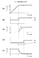
次に、バランス回路101〜10Nの動作を図5を参照して説明する。図5はその動作波形等を示しており、(A)は充電電圧の推移、(B)はトランジスタ74のスイッチング動作、(C)はバイパス電流の推移、(D)はトランジスタ86のスイッチング動作、(E)は充電電流の推移を示している。
Next, the operation of the
充電開始により、電気二重層コンデンサ401〜40Nに対し、充電回路6から定電流{図5の(E)}が流れる。この結果、図5の(A)に示すように、電気二重層コンデンサ401〜40Nの充電電圧が上昇する。その充電電圧が基準電圧VS (≡Vref )に到達すると、既述したように、ドライブ回路80が導通し、図5の(B)に示すように、トランジスタ74が時点t1 で導通し、バイパス動作を開始する。即ち、電気二重層コンデンサ401〜40Nに流れている電流はトランジスタ74の導通によりバイパス回路72に流れ、これがバイパス電流IB である。このバイパス電流IB は、図5の(C)に示すように、時点t1 から増加し、所定値として例えば、2〔A〕程度まで増加する。この結果、電気二重層コンデンサ401〜40Nの充電電流は、図5の(E)に示すように、時点t1 からバイパス電流IB の増加に応じて減少することになる。
When charging starts, a constant current {(E)} in FIG. 5 flows from the charging
このバイパス電流IB が所定値まで増加し、抵抗回路76の抵抗値RS との積で与えられる電圧VR が所定値VB に到達すると、その時点t2 でトランジスタ86が導通し{図5の(D)}、この結果、発光ダイオード161〜16N又は201〜20Nが発光し、受光トランジスタ181〜18N又は221〜22Nが導通する。これにより既述の充電回路6(図1)又はその制御部36(図2)に報知される。この報知に基づき、充電回路6では、その充電電流の段階的な減少等の制御が行われる。
When the bypass current I B increases to a predetermined value and the voltage V R given by the product of the resistance value R S of the
従って、電気二重層コンデンサ401〜40Nの充電電圧が所定電圧に到達したとき、即ち、バイパス回路72のバイパス動作に応動し、そのバイパス動作の開始(t1 )から所定時間Tだけ遅延した後、受光トランジスタ181〜18N又は221〜22Nが導通する。この場合、この遅延時間Tは、抵抗回路76の抵抗値RS によって任意に設定することができ、抵抗76A、76Bの抵抗値やその設置個数によって所望の値に設定することができる。
Accordingly, when the charging voltage of the electric
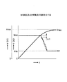
以上述べたバランス回路101〜10Nを用いた電気二重層コンデンサ装置2(図1)における電気二重層コンデンサの充電制御について、図6及び図7を参照して説明する。図6は、充電方法又は充電制御プログラムを示すフローチャート、図7は、電気二重層コンデンサの充電における電圧及び電流の推移を示す図である。
Charging control of the electric double layer capacitor in the electric double layer capacitor device 2 (FIG. 1) using the
説明を容易にするため、各電気二重層コンデンサ401〜40Nの未充電状態を想定すると、充電回路6からコンデンサ回路4に定電流として最大電流Imax を流し(ステップS1)、充電を行う。この充電により電気二重層コンデンサ401〜40Nの何れかの充電電圧が所定電圧に到達し、対応するバランス回路101〜10Nの何れかがバイパス動作に入ると(ステップS2)、現在の最大電流Imax から所定電流ΔIだけ低減させ(ステップS3)、電流(Imax −ΔI)で充電を持続する。各バランス回路101〜10Nのバイパス動作は既述の通りである。
For ease of explanation, assuming that the electric
そして、充電回路6からコンデンサ回路4に流れる電流が最低電流Imin に到達したか否かを判定し(ステップS4)、ステップS1〜ステップS3の処理を繰り返す。この結果、充電回路6からコンデンサ回路4に流れる電流は、バランス回路101〜10Nがバイパス動作に移行した数をNとすれば、電流(Imax −ΔI×N)となり、そのNに比例して段階的に減少することになる。この減少の結果、コンデンサ回路4に流れる電流が最低電流Imin に到達すると(ステップS4)、最低電流Imin に維持して(ステップS5)充電電圧を監視しながら充電を持続する。この結果、コンデンサ回路4の出力電圧VDC(=Vmax )、即ち、電気二重層コンデンサ401〜40Nの充電電圧が目標値に到達したか否かを判定し(ステップS6)、目標値に充電電圧が到達したとき、充電を完了する。この場合、各電気二重層コンデンサ401〜40Nの充電電圧の目標値は、電気二重層コンデンサ401〜40Nの直列個数をNとすれば、VDC/N(=Vmax /N)となる。
Then, whether a current flowing from the charging
斯かる構成とすれば、例えば、図7に示すように、充電電圧Vの推移に従い、バランス回路101〜10Nのバイパス動作に連動して最大電流Imax を最低電流Imin まで段階的に低減させ、最低電流Imin の持続により、コンデンサ回路4を最大電圧Vmax まで充電させ、これを出力電圧とすることができる。
With such a configuration, for example, as shown in FIG. 7, the maximum current I max is gradually reduced to the minimum current I min in conjunction with the bypass operation of the
そして、各バランス回路101〜10Nでは、各電気二重層コンデンサ401〜40Nが基準電圧VS に到達した後、遅延時間Tだけ制御部36へのバイパス動作の報知を遅延させているので、その遅延時間Tだけ充電が持続することになり、各電気二重層コンデンサ401〜40Nは十分な充電が行われ、所定の出力電圧VDCを得ることができる。
In each of the
なお、上記実施形態では、抵抗回路76の抵抗値RS とスイッチ回路84のトランジスタ86のスイッチング特性から所望の遅延時間Tを設定しているが、バイパス回路72のトランジスタ74とスイッチ回路84との間に遅延回路を介挿することにより、所望の遅延時間Tを設定するように構成してもよい。
In the above embodiment, the desired delay time T is set from the resistance value R S of the
また、上記実施形態では、ドライブ回路80としてシャントレギュレータ回路300を用いた例を記載したが、トランジスタ74を導通させる回路としては、電圧比較器のみを用いても構成でき、実施形態の回路に限定されるものではない。
In the above embodiment, an example in which the
また、上記実施形態では、充電回路6とバランス回路101〜10Nとを独立した構成として説明したが、充電回路6にバランス回路101〜10Nを内蔵した構成としてもよい。
In the above embodiment, the charging
(第2の実施形態)
本発明の第2の実施形態について、図8を参照して説明する。第2の実施形態は、既述のキャパシタ装置を用いた定着装置及びディジタル複写機について述べている。図8は、ディジタル複写機の概略構成例を示す縦断正面図である。このディジタル複写機410は、本発明の画像形成装置の一実施形態に係り、いわゆる複合機であって、複写機能と、これ以外の機能として例えば、プリンタ機能やファクシミリ機能を備えており、これら機能は図示しない操作部のアプリケーション切換えキーの操作によって選択することが可能である。この機能選択により、ディジタル複写機410は、複写機能の選択時に複写モード、プリンタ機能の選択時にプリントモード、ファクシミリ機能の選択時にファクシミリモードに切り換えられる。
(Second Embodiment)
A second embodiment of the present invention will be described with reference to FIG. In the second embodiment, a fixing device and a digital copying machine using the above-described capacitor device are described. FIG. 8 is a longitudinal sectional front view showing a schematic configuration example of the digital copying machine. This digital copying
このディジタル複写機410について、その構成とともに各種モードの動作を説明する。複写モードでは、原稿を送る自動原稿送り装置(以下「ADF」という)412の原稿台414に画像面を上にして置かれた原稿は、図示しない操作部上のスタートキーが押下されると、給紙ローラ416、給送ベルト418によってコンタクトガラス420上の所定の位置に給送される。ADF412は、一枚の原稿の給送完了毎に原稿枚数をカウントアップするカウント機能を有する。コンタクトガラス420上の原稿は、画像読取装置422によって画像情報が読み取られた後に、給送ベルト418、排送ローラ424によって排紙台426上に排出される。
The operation of various modes of the digital copying
画像読取装置422には、露光ランプ466、ミラー468、470、472、結像レンズ474、イメージセンサを構成するCCD(Charge Coupled device )476等が備えられている。光源である露光ランプ466により発せられた光が原稿に照射され、原稿からの反射光がミラー468、470、472を経て結像レンズ474で集光されてCCD476に検知され、光電変換により画像データに変換される。
The
原稿台414上に次の原稿が原稿セット検知器428で検知されると、同様に原稿台414上の一番下の原稿が給紙ローラ416、給送ベルト418によってコンタクトガラス420上の所定の位置に給送される。このコンタクトガラス420上の原稿は、画像読取装置422によって画像情報が読み取られた後に、給送ベルト418、排送ローラ424によって排紙台426上に排出される。給紙ローラ416、給送ベルト418及び排送ローラ424は図示しない搬送モータによって駆動される。
When the next document is detected by the document set
第1給紙装置430、第2給紙装置432及び第3給紙装置434は、それぞれ選択されたときに、その積載された転写紙を給紙する。この転写紙は縦搬送ユニット442によって感光体444に当接する位置まで搬送される。感光体444は、例えば感光体ドラムが用いられており、図示しないメインモータにより回転駆動される。
When selected, the first
画像読取装置422で原稿から読み取られた画像データは、画像処理部478で所定の画像処理が施された後、書込みユニット446によって光情報に変換される。その画像を表す光はミラー480を経て感光体444に照射される。感光体444には図示しない帯電器により一様に帯電された後、書込みユニット446からの光情報で露光されて静電潜像が形成される。この感光体444上の静電潜像は、現像装置448により現像されてトナー像となる。
Image data read from the document by the
このディジタル複写機410においては、書込みユニット446、感光体444、現像装置448や、その他の図示しない感光体444回りの周知の装置等により、電子写真方式で用紙等の媒体に画像形成を行うプリンタエンジンが構成されている。
In this digital copying
搬送ベルト450は、用紙搬送手段又は転写手段を構成しており、電源から転写バイアスが印加され、縦搬送ユニット442から搬送される転写媒体としての転写紙には、感光体444と等速で搬送されながら、感光体444上のトナー像が転写される。この転写紙は、定着装置452から加えられる熱によってトナー像を定着させ、排紙ユニット454により排紙トレイ456に排出される。感光体444にはトナー像転写後に図示しないクリーニング装置によりクリーニングが施され、感光体444上にある残存トナーが除去される。
The
このような複写動作は、通常モードでの用紙片面の複写である。この片面モードに対し、転写紙の両面に画像を複写する両面モードがある。この両面モードでは各給紙トレイ436〜440の何れかより給紙され、その表面に既述の画像が形成された転写紙は、両面入紙搬送路458側に切り換えられ、反転ユニット460によりスイッチバックされて表裏が反転され、両面搬送ユニット462へ搬送される。この場合、片面複写の排紙ユニット454による排紙トレイ456側への搬送が禁止される。
Such a copying operation is copying on one side of a sheet in the normal mode. In contrast to this single-side mode, there is a double-side mode in which an image is copied on both sides of a transfer sheet. In this double-sided mode, the transfer paper fed from any of the
両面搬送ユニット462へ搬送された転写紙は、両面搬送ユニット462により縦搬送ユニット442へ搬送され、感光体444に当接する。転写紙には、感光体444に形成されたトナー像が裏面に転写され、定着装置452によりトナー像が定着され、両面複写が得られる。この両面複写された転写紙は、排紙ユニット454により排紙トレイ456に排出される。
The transfer paper conveyed to the double-
また、転写紙を反転して排出する場合に、反転ユニット460によりスイッチバックされて表裏を反転させた転写紙は、反転排紙搬送路464を経て排紙ユニット454により排紙トレイ456に排出される。
When the transfer paper is reversed and discharged, the transfer paper that is switched back by the reversing
また、プリントモードでは、前述の画像処理装置からの画像データの代りに、外部からの画像データが書込みユニット446に入力され、複写モードと同様に転写紙上に画像が形成される。また、ファクシミリモードでは、画像読取装置422からの画像データが図示しないファクシミリ送受信部により相手に送信され、相手からの画像データがファクシミリ送受信部で受信されて前述の画像処理装置からの画像データの代りに書込みユニット446に入力されることにより、複写モードと同様に転写紙上に画像が形成される。
In the print mode, image data from the outside is input to the
また、ディジタル複写機410には、図示しない大量用紙供給装置(LCT)、ソート、穴あけ、ステイプル等を行うフィニッシャー、原稿読取りのためのモード、複写倍率の設定、給紙段数の設定、図示しないフィニッシャーで後処理の設定、オペレータに対する表示等を行う操作部を備える。
The
次に、このディジタル複写機410の定着装置452の構成について、図9を参照して説明する。図9は、定着装置452の基本的な構成を示している。この定着装置452では、定着部材である定着ローラ508に、加圧部材としての加圧ローラ510が、図示しない加圧手段により一定の加圧力を以て押し当てられている。加圧ローラ510は例えば、シリコンゴム等の弾性部材で構成される。定着部材と加圧部材は、双方をローラ状に構成する必要はなく、何れか一方又は双方を無端ベルトで構成してもよい。この定着装置452では、定着エネルギを発生する電熱源として例えば、交流(AC)定着ヒータHT1、HT2、HT3が設けられている。この実施形態では例えば、AC定着ヒータHT1、HT2、HT3は定着ローラ508の内部に配置されており、定着部材である定着ローラ508を内側から加熱する構成である。
Next, the configuration of the fixing
これら定着ローラ508及び加圧ローラ510は、図示しない駆動機構により回転駆動される。定着ローラ508の表面には定着温度を検出する手段として例えば、サーミスタ等の温度センサTH11、TH12が当接され、その表面温度が検出される。トナー512を担持した転写紙等の媒体であるシート514には、定着ローラ508と加圧ローラ510とのニップ部を通過する際に、定着ローラ508及び加圧ローラ510による加熱及び加圧によりトナー画像が定着する。
The fixing
そして、第2の発熱部材である複数本のAC定着ヒータHT2、HT3は、主たるヒータ(主ヒータ)を構成しており、定着ローラ508の基準となる目標温度に達していないときにONにされて、定着ローラ508を加熱する。これらAC定着ヒータHT2、HT3は例えば、定着ローラ508内において、B5サイズ、A4サイズ等を考慮して主走査方向を不均等に2分するように配置される。AC定着ヒータHT2は定着ローラ508の基準位置側からB5サイズ分、AC定着ヒータHT3は残りの(A4−B5)サイズ分を各々加熱するように割り当てられ、加熱むらを防止している。
The plurality of AC fixing heaters HT2 and HT3, which are the second heat generating members, constitute a main heater (main heater), and are turned on when the target temperature that is the reference of the fixing
第1の発熱部材であるAC定着ヒータHT1は、ディジタル複写機410の主電源投入時や、省エネのためのオフモード時からコピー可能となるまでの立上げ時等、定着装置452のウォームアップ時にONにされるか、又は、画像形成時に定着ローラ508の基準となる目標温度に達していないときにONされることにより、定着ローラ508を加熱する補助的なヒータ(補助ヒータ)である。
The AC fixing heater HT1, which is the first heat generating member, is used when the fixing
次に、ディジタル複写機410の電源制御系の構成について、図10を参照して説明する。図10は、ディジタル複写機410の定着装置452の電源回路482の構成を示すブロック図である。
Next, the configuration of the power supply control system of the digital copying
この電源回路482には例えば、商用交流電源等のAC電源PSの供給のON/OFFを行うメイン電源スイッチ(SW)484が設けられ、このSW484を通してAC電源PSが制御部486、キャパシタ充電回路488、直流(DC)電源生成回路490、ACヒータ駆動回路492に加えられている。制御部486は電源回路482の各部その他を制御し、キャパシタ充電回路488は、既述の充電回路6(図1、図2)で構成され、AC電源PSを受けてキャパシタ装置493を充電する。このキャパシタ装置493は、既述のコンデンサ回路4(図1、図2)で構成され、AC定着ヒータHT1の補助電源を構成する。DC電源生成回路490は、ディジタル複写機410のDC電源を生成する。ACヒータ駆動回路492は、AC定着ヒータHT2、HT3にAC電力を供給する第2の駆動回路を構成する。このACヒータ駆動回路492の出力はインターロックスイッチ494を介してACヒータ駆動回路492及びキャパシタ放電回路496に加えられている。そして、キャパシタ放電回路496は、キャパシタ装置493の放電を実行し、AC定着ヒータHT1に対してDC電力を供給する第1の駆動回路を構成している。
The
そして、制御部486は、電源回路482の各部を制御しており、キャパシタ充電回路488、ACヒータ駆動回路492及びキャパシタ放電回路496の動作を制御する。この制御動作として例えば、キャパシタ充電回路488に制御信号S1を送出して、キャパシタ充電回路488によるキャパシタ装置493の充電動作を制御する。また、キャパシタ放電回路496に、制御信号S3、S4を送出して、キャパシタ放電回路496によるAC定着ヒータHT1のON/OFF動作を制御する。また、制御信号S8、S9、S10をACヒータ駆動回路492に送出し、ACヒータ駆動回路492によるAC定着ヒータHT2、HT3のON/OFF動作を制御する。
The
DC電源生成回路490は、メイン電源SW484を介して入力されるAC電源に基づいて、画像形成装置の制御系に供給する電源VCCと、駆動系、中高圧電源に供給する電源Vaaを生成している。
The DC
インターロックスイッチ494は、このディジタル複写機410のカバー類(図示せず)と連動してON/OFFするスイッチであり、ディジタル複写機410のカバー類が開放されることにより触れることができる駆動部材、中高圧電源印加部材を有する場合に、カバー開時に該駆動部材の動作を停止又は該印加部材への電圧印加を停止するよう電源を遮断する構成となっている。インターロックスイッチ494にはDC電源生成回路490で生成された電源Vaaの一部が入力され、このインターロックスイッチ494を介して、キャパシタ放電回路496及びACヒータ駆動回路492に入力される。
The
ACヒータ駆動回路492は、制御部486から入力される制御信号S8、S9、S10に応じて、AC定着ヒータHT2、HT3のON/OFFを行う。キャパシタ充電回路488は、キャパシタ装置493と接続されており、制御部486から入力される制御信号S1に基づいて、キャパシタ装置493の充電を行う。キャパシタ装置493は、電気二重層コンデンサ等の大容量のキャパシタで構成されている。キャパシタ装置493は、キャパシタ充電回路488及びキャパシタ放電回路496に接続されており、キャパシタ充電回路488から充電が行われる。キャパシタ装置493に充電された電力は、キャパシタ放電回路496のON/OFF制御によりAC定着ヒータHT1に供給される。
The AC
キャパシタ放電回路496は、制御部486から入力される制御信号S3、S4に応じて、キャパシタ装置493に蓄積された電力が定着ヒータHT1に供給され、定着ヒータHT1をON/OFFさせる。温度センサTH11、TH12は、既述したように、定着ローラ508の近傍に設置され、定着ローラ508の表面温度を表す検出信号S6a、S6bが得られ、各検出信号S6a、S6bが制御部486に制御情報として加えられる。この場合、温度センサTH11、TH12の抵抗値が検出温度により変化するので、制御部486は、これら温度センサTH11、TH12の抵抗値の温度変化を利用し、その抵抗値変化を以て定着ローラ508の表面温度を検出する。温度センサTH11は例えば、定着ヒータHT2の加熱領域に対応して配置され、温度センサTH12は例えば、定着ヒータHT3の加熱領域に対応して配置されている。
The
次に、ACヒータ駆動回路492(図10)の構成について、図11を参照して説明する。図11は、ACヒータ駆動回路492の構成例を示す回路図である。
Next, the configuration of the AC heater drive circuit 492 (FIG. 10) will be described with reference to FIG. FIG. 11 is a circuit diagram illustrating a configuration example of the AC
このACヒータ駆動回路492には、入力されるAC電源PSのノイズを除去するフィルタFIL21が設置され、制御部486から入力される制御信号S9に応じて、ON/OFFされる安全保護用の定着リレーRL21が設置されている。この定着リレーRL21には逆起防止用のダイオードD21が接続され、制御部486から入力される制御信号S8、S10に基づいて、定着ヒータHT2、HT3をON/OFFさせるヒータON/OFF回路500、502が設置されている。
The AC
AC電源PSには、フィルタFIL21、定着リレーRL21及びヒータON/OFF回路500を介して定着ヒータHT2が接続されているとともに、フィルタFIL21、定着リレーRL21及びヒータON/OFF回路502を介して定着ヒータHT3が接続されている。
The AC power source PS is connected to a fixing heater HT2 via a filter FIL21, a fixing relay RL21, and a heater ON /
ヒータON/OFF回路500は、トライアックTR121、フォトカプラPC21、トランジスタTR21、ノイズ吸収用スナバ回路503、インダクタL21、抵抗R22、R23、R24で構成されている。トライアックTR121はAC電源PSをON/OFFするためのスイッチであり、フォトカプラPC21は、トライアックTR121のベースをONし、また、2次側である制御部486からの信号を絶縁する。トランジスタTR21は、フォトカプラPC21の発光側LEDを駆動するためのドライバであり、ノイズ吸収用スナバ回路503はコンデンサC21及び抵抗R21で構成されている。インダクタL21はノイズ吸収用であり、抵抗R22は続流防止抵抗である。抵抗R23、R24はフォトカプラPC21の電流制限抵抗である。
The heater ON /
ヒータON/OFF回路502も同様に、トライアックTR131、フォトカプラPC31、トランジスタTR31、ノイズ吸収用スナバ回路505、インダクタL31、抵抗R32、R33、R34で構成されている。トライアックTR131はAC電源PSをON/OFFするためのスイッチであり、フォトカプラPC31は、トライアックTRI31のベースをONし、また、2次側である制御部486からの信号を絶縁する。トランジスタTR31は、フォトカプラPC31の発光側LEDを駆動するためのドライバであり、ノイズ吸収用スナバ回路505は、コンデンサC31及び抵抗R31で構成されている。インダクタL31はノイズ吸収用であり、抵抗R32は、続流防止抵抗である。抵抗R33、R34はフォトカプラPC31の電流制限抵抗である。
Similarly, the heater ON /
上記構成のACヒータ駆動回路492において、定着ヒータHT2は定着リレーRL21とトランジスタTR21のベースの双方がONされた状態で電力が供給されて点灯する。同様に、定着ヒータHT3は定着リレーRL21とトランジスタTR31のベースの双方がONされた状態で電力が供給されて点灯する。
In the AC
制御部486は、定着リレーRL21に供給する制御信号S9をONした状態で、ヒータON/OFF回路500のトランジスタTR21のベースに供給する制御信号S8をON/OFFさせ、定着ヒータHT2の点灯/消灯を制御する。同様に、制御部486は、定着リレーRL21に供給する制御信号S9をONした状態で、ヒータON/OFF回路502のトランジスタTR31のベースに供給する制御信号S10をON/OFFして、定着ヒータHT3の点灯/消灯を制御する。
The
次に、キャパシタ放電回路496(図10)について、図12を参照して説明する。図12は、キャパシタ放電回路496の構成を示すブロック図である。
Next, the capacitor discharge circuit 496 (FIG. 10) will be described with reference to FIG. FIG. 12 is a block diagram showing a configuration of the
キャパシタ放電回路496は、充放電用スイッチ504、安全保護用の定着リレーRL11、定着リレーRL11の逆起防止用のダイオードD11、キャパシタ装置493の両端電圧を検出する両端電圧検出回路506を備えている。
The
キャパシタ装置193の両端には、充放電用スイッチ504と定着リレーRL11が接続されている。充放電用スイッチ504は、制御部486から入力される制御信号S3によりON/OFFされる。同様に、定着リレーRL11は、制御部486から入力される制御信号S4によりON/OFFされる。充放電用スイッチ504と定着リレーRL11の両者がONされると、キャパシタ装置493に蓄積された電荷が放電して、定着ヒータHT1に電力が供給される。
A charging / discharging
そして、両端電圧検出回路506は、キャパシタ装置493の両端電圧を検出して、その検出信号S5を制御部486に出力する。制御部486は、この検出信号S5を常時監視して、キャパシタ装置493の充電状態を監視している。
Then, the both-end
以上述べた通り、このようなディジタル複写機410によれば、キャパシタ装置493に電気二重層コンデンサ装置2(図1)、キャパシタ充電回路488に充電回路6(図2等)を使用することにより、第1の実施形態で述べた通りの作用効果が期待できる。そして、ディジタル複写機410においては、キャパシタ装置493の電力をキャパシタ放電回路496を通して放電することにより、定着装置452の定着ヒータHT1を予備加熱することができる。この結果、複写開始動作を迅速化することができる。
As described above, according to such a digital copying
既述した通り、このようなキャパシタ装置493に既述の電気二重層コンデンサ装置2を用いるので、定電力充電によって商用交流電源の給電許容量を超えることがなく、また、ディジタル複写機410の各部に対する電力配分を適正且つ効率的に行うことができる。
As described above, since the electric double
特に、既述の作用に記載した通り、一定の充電電圧として例えば、28〔V〕を境にして定電流充電から定電力充電に切り換え、一定の充電電圧として例えば、44〔V〕に達した後、定電力充電から定電流充電に再度切り換えるので、キャパシタ装置493を効率よく、しかも、商用交流電源の給電許容量を超えることなく、満充電を達成でき、定着装置452の定着ヒータHT1の予備加熱を効率よく行うことができる。
In particular, as described in the above-described operation, the constant charging voltage is switched from constant current charging to constant power charging at, for example, 28 [V], and the constant charging voltage reaches, for example, 44 [V]. Thereafter, switching from constant power charging to constant current charging is performed again, so that the
なお、第1の実施形態では、電気二重層コンデンサ装置2、電気二重層コンデンサ401〜40Nについて説明し、第2の実施形態では、キャパシタ装置493やキャパシタ充電回路488、キャパシタ放電回路496について説明しているが、定着装置452の定着ヒータHT1の予備加熱に用いるキャパシタ装置493には電気二重層コンデンサ以外のキャパシタを用いてもよい。
In the first embodiment, the electric double
また、上記実施形態では、電気二重層コンデンサ装置2を例示して説明したが、この電気二重層コンデンサ装置2は複写機、ファクシミリ装置、プリンタ装置等の画像形成装置、その他の電源装置等に用いることができる。
In the above-described embodiment, the electric double
以上述べたように、本発明の最も好ましい実施形態等について説明したが、本発明は上記記載に限定されるものではなく、特許請求の範囲に記載され、又は、発明を実施するための最良の形態に開示された発明の要旨に基づき、当業者において様々な変形や変更が可能であり、斯かる変形や変更が本発明の範囲に含まれることはいうまでもない。
As described above, the most preferred embodiment of the present invention has been described. However, the present invention is not limited to the above description, and is described in the claims or the best for carrying out the invention. Various modifications and changes can be made by those skilled in the art based on the gist of the invention disclosed in the embodiments, and it goes without saying that such modifications and changes are included in the scope of the present invention.
本発明によれば、単一又は複数のキャパシタの充電に関し、定電流充電、キャパシタに併設したバイパス手段のバイパス動作の開始と充電電流の低減との間に時間差を設定しているので、効率的な充電を行うことができ、高効率、信頼性、安全性の高いキャパシタ装置、定着装置及び画像形成装置の実現に寄与し、有用である。
According to the present invention, with respect to charging of one or a plurality of capacitors, since a time difference is set between constant current charging, start of bypass operation of the bypass means provided in the capacitor and reduction of charging current, it is efficient. Can be charged efficiently and contributes to the realization of a capacitor device, a fixing device, and an image forming apparatus with high efficiency, reliability, and safety, which are useful.
2 電気二重層コンデンサ装置
6 充電回路
36 制御部
70 出力回路
72 バイパス回路
74 トランジスタ(第1のスイッチング素子)
76 抵抗回路
76A、76B 抵抗
81、82 抵抗(電圧検出手段)
86 トランジスタ(第2のスイッチング素子)
101〜10N バランス回路(バイパス手段)
121〜12N、141〜14N フォトカプラ
302 電圧比較器(電圧検出手段)
401〜40N 電気二重層コンデンサ
410 ディジタル複写機(画像形成装置)
488 キャパシタ充電回路
493 キャパシタ装置
496 キャパシタ放電回路
2 Electric Double
76
86 transistor (second switching element)
101-10N balance circuit (bypass means)
121-12N, 141-
401 to 40N Electric
488
Claims (18)
直列化された複数のキャパシタの直列回路に電流を流す充電手段と、
前記キャパシタに個別に並列に接続されて前記キャパシタが基準電圧に到達したとき、対応するキャパシタの前記電流を分流させるバイパス手段と、
このバイパス手段のバイパス動作から所定時間だけ遅延して前記バイパス手段がバイパス動作を開始したことを表す出力を発生させ、前記充電手段が前記キャパシタの前記直列回路に流す電流を低減させる出力手段と、
を備え、前記バイパス手段のバイパス動作に対して前記キャパシタの前記直列回路に流す電流の低減との間に所定の時間差を設定させたことを特徴とするキャパシタ装置。 A capacitor device comprising a plurality of capacitors connected in series and charging each capacitor to a predetermined voltage,
Charging means for passing current through a series circuit of a plurality of capacitors in series;
Bypass means for individually connecting to the capacitor in parallel and diverting the current of the corresponding capacitor when the capacitor reaches a reference voltage;
The from the bypass operation of the bypass means is delayed by a predetermined time to generate an output indicating that said bypass means has started a bypass operation, and output means the Ru reduces the current flowing to the series circuit of the charging means the capacitor ,
A capacitor device, wherein a predetermined time difference is set between the bypass operation of the bypass means and the reduction of the current flowing through the series circuit of the capacitor.
直列化された複数のキャパシタの直列回路に電流を流す充電手段と、
前記キャパシタに個別に並列に接続されて前記キャパシタが基準電圧に到達したとき、対応するキャパシタの前記電流を分流させるバイパス手段とを備え、前記バイパス手段が、
前記キャパシタの充電電圧を検出する電圧検出手段と、
この電圧検出手段の検出出力を受け、前記充電電圧が前記所定電圧に到達したとき、前記キャパシタにバイパス路を形成する第1のスイッチング素子と、
この第1のスイッチング素子から所定時間だけ遅延してスイッチングし、前記第1のスイッチング素子が前記バイパス動作を開始したことを表す出力を発生する第2のスイッチング素子と、
を備えることにより、前記第2のスイッチング素子の前記出力により前記充電手段の前記電流を低減させる構成としたことを特徴とするキャパシタ装置。 A capacitor device comprising a plurality of capacitors connected in series and charging each capacitor to a predetermined voltage,
Charging means for passing current through a series circuit of a plurality of capacitors in series;
Bypass means for shunting the current of the corresponding capacitor when the capacitor reaches a reference voltage individually connected in parallel to the capacitor, and the bypass means,
Voltage detecting means for detecting a charging voltage of the capacitor;
A first switching element that receives a detection output of the voltage detection means and forms a bypass path in the capacitor when the charging voltage reaches the predetermined voltage;
A second switching element that switches by a predetermined time from the first switching element and generates an output indicating that the first switching element has started the bypass operation;
The capacitor device is configured to reduce the current of the charging unit by the output of the second switching element.
前記トナー像を加熱する加熱手段と、
この加熱手段の給電部に電気エネルギを供給するキャパシタ装置と、
を備え、該キャパシタ装置が、
直列に接続されて所定電圧に充電される複数のキャパシタと、
前記キャパシタの直列回路に電流を流し、キャパシタを所定電圧に充電させる充電手段と、
前記キャパシタに個別に並列に接続されて前記キャパシタが基準電圧に到達したとき、対応するキャパシタの前記電流を分流させるバイパス手段と、
このバイパス手段のバイパス動作から所定時間だけ遅延して前記バイパス手段がバイパス動作を開始したことを表す出力を発生させ、前記充電手段が前記キャパシタの前記直列回路に流す電流を低減させる出力手段と、
を備え、前記バイパス手段のバイパス動作に対して前記キャパシタの前記直列回路に流す電流の低減との間に所定の時間差を設定させた構成としたことを特徴とする定着装置。 A fixing device for fixing a toner image to a transfer medium by heating,
Heating means for heating the toner image;
A capacitor device for supplying electrical energy to the power feeding portion of the heating means;
Comprising the capacitor device,
A plurality of capacitors connected in series and charged to a predetermined voltage;
Charging means for passing a current through a series circuit of the capacitor and charging the capacitor to a predetermined voltage;
Bypass means for individually connecting to the capacitor in parallel and diverting the current of the corresponding capacitor when the capacitor reaches a reference voltage;
The from the bypass operation of the bypass means is delayed by a predetermined time to generate an output indicating that said bypass means has started a bypass operation, and output means the Ru reduces the current flowing to the series circuit of the charging means the capacitor ,
The fixing device is configured to set a predetermined time difference between the bypass operation of the bypass unit and the reduction of the current flowing through the series circuit of the capacitor.
前記トナー像を加熱する加熱手段と、
この加熱手段の給電部に電気エネルギを供給するキャパシタ装置と、
を備え、該キャパシタ装置が、
直列に接続されて所定電圧に充電される複数のキャパシタと、
前記キャパシタの直列回路に電流を流し、キャパシタを所定電圧に充電させる充電手段と、
前記キャパシタに個別に並列に接続されて前記キャパシタが基準電圧に到達したとき、対応するキャパシタの前記電流を分流させるバイパス手段とを備え、前記バイパス手段が、
前記キャパシタの充電電圧を検出する電圧検出手段と、
この電圧検出手段の検出出力を受け、前記充電電圧が前記所定電圧に到達したとき、前記キャパシタにバイパス路を形成する第1のスイッチング素子と、
この第1のスイッチング素子から所定時間だけ遅延してスイッチングし、前記第1のスイッチング素子が前記バイパス動作を開始したことを表す出力を発生する第2のスイッチング素子と、
を備えることにより、前記第2のスイッチング素子の前記出力により前記充電手段の前記電流を低減させる構成としたことを特徴とする定着装置。 A fixing device for fixing a toner image to a transfer medium by heating,
Heating means for heating the toner image;
A capacitor device for supplying electrical energy to the power feeding portion of the heating means;
Comprising the capacitor device,
A plurality of capacitors connected in series and charged to a predetermined voltage;
Charging means for passing a current through a series circuit of the capacitor and charging the capacitor to a predetermined voltage;
Bypass means for shunting the current of the corresponding capacitor when the capacitor reaches a reference voltage individually connected in parallel to the capacitor, and the bypass means,
Voltage detecting means for detecting a charging voltage of the capacitor;
A first switching element that receives a detection output of the voltage detection means and forms a bypass path in the capacitor when the charging voltage reaches the predetermined voltage;
A second switching element that switches by a predetermined time from the first switching element and generates an output indicating that the first switching element has started the bypass operation;
The fixing device is configured to reduce the current of the charging unit by the output of the second switching element.
前記定着装置の給電部にキャパシタ装置を備え、該キャパシタ装置が、
直列に接続されて所定電圧に充電される複数のキャパシタと、
前記キャパシタの直列回路に電流を流し、キャパシタを所定電圧に充電させる充電手段と、
前記キャパシタに個別に並列に接続されて前記キャパシタが基準電圧に到達したとき、対応するキャパシタの前記電流を分流させるバイパス手段と、
このバイパス手段のバイパス動作から所定時間だけ遅延して前記バイパス手段がバイパス動作を開始したことを表す出力を発生させ、前記充電手段が前記キャパシタの前記直列回路に流す電流を低減させる出力手段と、
を備え、前記バイパス手段のバイパス動作に対して前記キャパシタの前記直列回路に流す電流の低減との間に所定の時間差を設定させた構成としたことを特徴とする画像形成装置。 An image forming apparatus including a fixing device that fixes a toner image to a transfer medium by electroheating,
The power supply unit of the fixing device includes a capacitor device, and the capacitor device includes:
A plurality of capacitors connected in series and charged to a predetermined voltage;
Charging means for passing a current through a series circuit of the capacitor and charging the capacitor to a predetermined voltage;
Bypass means for individually connecting to the capacitor in parallel and diverting the current of the corresponding capacitor when the capacitor reaches a reference voltage;
The from the bypass operation of the bypass means is delayed by a predetermined time to generate an output indicating that said bypass means has started a bypass operation, and output means the Ru reduces the current flowing to the series circuit of the charging means the capacitor ,
An image forming apparatus characterized in that a predetermined time difference is set between the bypass operation of the bypass means and the reduction of the current flowing through the series circuit of the capacitor.
前記定着装置の給電部にキャパシタ装置を備え、該キャパシタ装置が、
直列に接続されて所定電圧に充電される複数のキャパシタと、
前記キャパシタの直列回路に電流を流し、キャパシタを所定電圧に充電させる充電手段と、
前記キャパシタに個別に並列に接続されて前記キャパシタが基準電圧に到達したとき、対応するキャパシタの前記電流を分流させるバイパス手段とを備え、前記バイパス手段が、
前記キャパシタの充電電圧を検出する電圧検出手段と、
この電圧検出手段の検出出力を受け、前記充電電圧が前記所定電圧に到達したとき、前記キャパシタにバイパス路を形成する第1のスイッチング素子と、
この第1のスイッチング素子から所定時間だけ遅延してスイッチングし、前記第1のスイッチング素子が前記バイパス動作を開始したことを表す出力を発生する第2のスイッチング素子と、
を備えることにより、前記第2のスイッチング素子の前記出力により前記充電手段の前記電流を低減させる構成としたことを特徴とする画像形成装置。 An image forming apparatus including a fixing device that fixes a toner image to a transfer medium by electroheating,
The power supply unit of the fixing device includes a capacitor device, and the capacitor device includes:
A plurality of capacitors connected in series and charged to a predetermined voltage;
Charging means for passing a current through a series circuit of the capacitor and charging the capacitor to a predetermined voltage;
Bypass means for shunting the current of the corresponding capacitor when the capacitor reaches a reference voltage individually connected in parallel to the capacitor, and the bypass means,
Voltage detecting means for detecting a charging voltage of the capacitor;
A first switching element that receives a detection output of the voltage detection means and forms a bypass path in the capacitor when the charging voltage reaches the predetermined voltage;
A second switching element that switches by a predetermined time from the first switching element and generates an output indicating that the first switching element has started the bypass operation;
The image forming apparatus is configured to reduce the current of the charging unit by the output of the second switching element.
Priority Applications (1)
| Application Number | Priority Date | Filing Date | Title |
|---|---|---|---|
| JP2005026574A JP4659472B2 (en) | 2004-02-03 | 2005-02-02 | Capacitor device, fixing device, and image forming apparatus |
Applications Claiming Priority (2)
| Application Number | Priority Date | Filing Date | Title |
|---|---|---|---|
| JP2004027365 | 2004-02-03 | ||
| JP2005026574A JP4659472B2 (en) | 2004-02-03 | 2005-02-02 | Capacitor device, fixing device, and image forming apparatus |
Publications (2)
| Publication Number | Publication Date |
|---|---|
| JP2005253291A JP2005253291A (en) | 2005-09-15 |
| JP4659472B2 true JP4659472B2 (en) | 2011-03-30 |
Family
ID=35033237
Family Applications (1)
| Application Number | Title | Priority Date | Filing Date |
|---|---|---|---|
| JP2005026574A Active JP4659472B2 (en) | 2004-02-03 | 2005-02-02 | Capacitor device, fixing device, and image forming apparatus |
Country Status (1)
| Country | Link |
|---|---|
| JP (1) | JP4659472B2 (en) |
Families Citing this family (8)
| Publication number | Priority date | Publication date | Assignee | Title |
|---|---|---|---|---|
| DE60336209D1 (en) * | 2002-02-04 | 2011-04-14 | Ricoh Co Ltd | HEATING DEVICE, FIXING DEVICE AND PICTURE GENERATING DEVICE |
| JP4600171B2 (en) * | 2005-06-22 | 2010-12-15 | 富士ゼロックス株式会社 | Fixing device and fixing roller heating method |
| JP4824396B2 (en) * | 2005-12-19 | 2011-11-30 | 株式会社リコー | Image forming apparatus |
| JP2008245434A (en) * | 2007-03-27 | 2008-10-09 | Nippon Chemicon Corp | Apparatus for charging electric double layer capacitor and its charging control method |
| KR100814824B1 (en) * | 2007-05-03 | 2008-03-20 | 삼성에스디아이 주식회사 | Plasma display and driving method thereof |
| JP4944236B2 (en) * | 2010-09-27 | 2012-05-30 | 株式会社リコー | Image forming apparatus |
| JP6598511B2 (en) * | 2015-05-21 | 2019-10-30 | キヤノン株式会社 | Power supply device and image forming apparatus |
| US10998824B2 (en) * | 2016-03-22 | 2021-05-04 | Mitsubishi Electric Corporation | Electric power conversion device |
Citations (5)
| Publication number | Priority date | Publication date | Assignee | Title |
|---|---|---|---|---|
| JPH0629391U (en) * | 1992-09-16 | 1994-04-15 | 株式会社明電舎 | IGBT element damage detection circuit |
| JP2000050496A (en) * | 1998-07-30 | 2000-02-18 | Kansai Coke & Chem Co Ltd | Charge control device for electric double-layer capacitor |
| JP2000116025A (en) * | 1998-10-06 | 2000-04-21 | Hitachi Ltd | Recharging device |
| JP2003244859A (en) * | 2002-02-19 | 2003-08-29 | Nichicon Corp | Method of charging electric double-layer capacitor |
| JP2003297526A (en) * | 2001-05-30 | 2003-10-17 | Ricoh Co Ltd | Heating device, fixing device and image forming device |
Family Cites Families (1)
| Publication number | Priority date | Publication date | Assignee | Title |
|---|---|---|---|---|
| JPS6237063A (en) * | 1985-08-07 | 1987-02-18 | Nec Corp | Switching regulator |
-
2005
- 2005-02-02 JP JP2005026574A patent/JP4659472B2/en active Active
Patent Citations (5)
| Publication number | Priority date | Publication date | Assignee | Title |
|---|---|---|---|---|
| JPH0629391U (en) * | 1992-09-16 | 1994-04-15 | 株式会社明電舎 | IGBT element damage detection circuit |
| JP2000050496A (en) * | 1998-07-30 | 2000-02-18 | Kansai Coke & Chem Co Ltd | Charge control device for electric double-layer capacitor |
| JP2000116025A (en) * | 1998-10-06 | 2000-04-21 | Hitachi Ltd | Recharging device |
| JP2003297526A (en) * | 2001-05-30 | 2003-10-17 | Ricoh Co Ltd | Heating device, fixing device and image forming device |
| JP2003244859A (en) * | 2002-02-19 | 2003-08-29 | Nichicon Corp | Method of charging electric double-layer capacitor |
Also Published As
| Publication number | Publication date |
|---|---|
| JP2005253291A (en) | 2005-09-15 |
Similar Documents
| Publication | Publication Date | Title |
|---|---|---|
| JP4659472B2 (en) | Capacitor device, fixing device, and image forming apparatus | |
| JP5019814B2 (en) | Image forming apparatus and power control method | |
| US8008892B2 (en) | Image forming apparatus, power supply device, and control method | |
| JP4531487B2 (en) | Fixing apparatus and image forming apparatus | |
| US7269368B2 (en) | Image forming apparatus for forming image with fixing member, power supply control method for controlling the image forming apparatus, and power supply control program for controlling the image forming apparatus | |
| US7127189B2 (en) | Heating unit, auxiliary power unit, fixing unit, and image forming apparatus | |
| JP4148943B2 (en) | Auxiliary power supply device, fixing device, image forming apparatus, and charging operation control method | |
| JP4690736B2 (en) | Capacitor device charging circuit, charging method, charging control device, control program, capacitor device, fixing device, and image forming apparatus | |
| JP4931354B2 (en) | Capacitor charging circuit, charging method, charging control device, control program, capacitor device, fixing device, and image forming apparatus | |
| JP5614103B2 (en) | Charging apparatus, image forming apparatus, and program | |
| JP6195358B2 (en) | Image forming apparatus | |
| JP2006288090A (en) | Capacitor apparatus, charging method for the same and image forming apparatus | |
| JP2005032558A (en) | Heating device, fixing device, and image forming device | |
| JP4317151B2 (en) | Power storage device and image forming apparatus | |
| JP2005253290A (en) | Capacitor device, fixing device and image forming apparatus | |
| US9535379B2 (en) | Image forming apparatus with warmup power control and connectable option device | |
| JP2007316168A (en) | Image forming apparatus and image forming method | |
| JP4295534B2 (en) | Image forming apparatus and charger | |
| JP4112381B2 (en) | Fixing apparatus and image forming apparatus | |
| JP2004286881A (en) | Image forming apparatus | |
| JP5015342B2 (en) | Image forming apparatus | |
| US20150092211A1 (en) | Image forming apparatus | |
| JP4154320B2 (en) | Power supply device and image forming apparatus provided with the power supply device | |
| JP2005223984A (en) | Heat generating unit, fixing device, and image forming apparatus | |
| JP2018007488A (en) | Charging device and image forming apparatus |
Legal Events
| Date | Code | Title | Description |
|---|---|---|---|
| A621 | Written request for application examination |
Free format text: JAPANESE INTERMEDIATE CODE: A621 Effective date: 20080122 |
|
| A977 | Report on retrieval |
Free format text: JAPANESE INTERMEDIATE CODE: A971007 Effective date: 20100909 |
|
| A131 | Notification of reasons for refusal |
Free format text: JAPANESE INTERMEDIATE CODE: A131 Effective date: 20100928 |
|
| A521 | Request for written amendment filed |
Free format text: JAPANESE INTERMEDIATE CODE: A523 Effective date: 20101129 |
|
| TRDD | Decision of grant or rejection written | ||
| A01 | Written decision to grant a patent or to grant a registration (utility model) |
Free format text: JAPANESE INTERMEDIATE CODE: A01 Effective date: 20101221 |
|
| A01 | Written decision to grant a patent or to grant a registration (utility model) |
Free format text: JAPANESE INTERMEDIATE CODE: A01 |
|
| A61 | First payment of annual fees (during grant procedure) |
Free format text: JAPANESE INTERMEDIATE CODE: A61 Effective date: 20101227 |
|
| FPAY | Renewal fee payment (event date is renewal date of database) |
Free format text: PAYMENT UNTIL: 20140107 Year of fee payment: 3 |
|
| R150 | Certificate of patent or registration of utility model |
Ref document number: 4659472 Country of ref document: JP Free format text: JAPANESE INTERMEDIATE CODE: R150 Free format text: JAPANESE INTERMEDIATE CODE: R150 |
|
| R250 | Receipt of annual fees |
Free format text: JAPANESE INTERMEDIATE CODE: R250 |
|
| R250 | Receipt of annual fees |
Free format text: JAPANESE INTERMEDIATE CODE: R250 |
|
| R250 | Receipt of annual fees |
Free format text: JAPANESE INTERMEDIATE CODE: R250 |
|
| R250 | Receipt of annual fees |
Free format text: JAPANESE INTERMEDIATE CODE: R250 |
|
| R250 | Receipt of annual fees |
Free format text: JAPANESE INTERMEDIATE CODE: R250 |
|
| R250 | Receipt of annual fees |
Free format text: JAPANESE INTERMEDIATE CODE: R250 |
|
| R250 | Receipt of annual fees |
Free format text: JAPANESE INTERMEDIATE CODE: R250 |
|
| R250 | Receipt of annual fees |
Free format text: JAPANESE INTERMEDIATE CODE: R250 |
|
| R250 | Receipt of annual fees |
Free format text: JAPANESE INTERMEDIATE CODE: R250 |
|
| R250 | Receipt of annual fees |
Free format text: JAPANESE INTERMEDIATE CODE: R250 |
|
| R250 | Receipt of annual fees |
Free format text: JAPANESE INTERMEDIATE CODE: R250 |