JP4657512B2 - Organic light emitting device - Google Patents
Organic light emitting device Download PDFInfo
- Publication number
- JP4657512B2 JP4657512B2 JP2001217393A JP2001217393A JP4657512B2 JP 4657512 B2 JP4657512 B2 JP 4657512B2 JP 2001217393 A JP2001217393 A JP 2001217393A JP 2001217393 A JP2001217393 A JP 2001217393A JP 4657512 B2 JP4657512 B2 JP 4657512B2
- Authority
- JP
- Japan
- Prior art keywords
- light emitting
- organic light
- emitting device
- region
- annealing
- Prior art date
- Legal status (The legal status is an assumption and is not a legal conclusion. Google has not performed a legal analysis and makes no representation as to the accuracy of the status listed.)
- Expired - Lifetime
Links
- 239000000463 material Substances 0.000 claims description 128
- 238000000137 annealing Methods 0.000 claims description 77
- 230000005525 hole transport Effects 0.000 claims description 63
- 238000000034 method Methods 0.000 claims description 21
- 238000004519 manufacturing process Methods 0.000 claims description 12
- 239000000203 mixture Substances 0.000 claims description 12
- 239000002019 doping agent Substances 0.000 claims description 5
- TVIVIEFSHFOWTE-UHFFFAOYSA-K tri(quinolin-8-yloxy)alumane Chemical compound [Al+3].C1=CN=C2C([O-])=CC=CC2=C1.C1=CN=C2C([O-])=CC=CC2=C1.C1=CN=C2C([O-])=CC=CC2=C1 TVIVIEFSHFOWTE-UHFFFAOYSA-K 0.000 claims description 4
- HFACYLZERDEVSX-UHFFFAOYSA-N benzidine Chemical class C1=CC(N)=CC=C1C1=CC=C(N)C=C1 HFACYLZERDEVSX-UHFFFAOYSA-N 0.000 claims description 3
- PJVZQNVOUCOJGE-CALCHBBNSA-N chembl289853 Chemical class N1([C@H]2CC[C@H](O2)N2[C]3C=CC=CC3=C3C2=C11)C2=CC=C[CH]C2=C1C1=C3C(=O)N(C)C1=O PJVZQNVOUCOJGE-CALCHBBNSA-N 0.000 claims description 3
- 229910052757 nitrogen Inorganic materials 0.000 description 41
- -1 polyphenylene vinylenes Polymers 0.000 description 36
- 238000006243 chemical reaction Methods 0.000 description 28
- 229910052751 metal Inorganic materials 0.000 description 23
- 239000002184 metal Substances 0.000 description 23
- 239000000758 substrate Substances 0.000 description 19
- HCHKCACWOHOZIP-UHFFFAOYSA-N Zinc Chemical compound [Zn] HCHKCACWOHOZIP-UHFFFAOYSA-N 0.000 description 14
- 229910052725 zinc Inorganic materials 0.000 description 14
- 239000011701 zinc Substances 0.000 description 14
- 229910052790 beryllium Inorganic materials 0.000 description 11
- ATBAMAFKBVZNFJ-UHFFFAOYSA-N beryllium atom Chemical compound [Be] ATBAMAFKBVZNFJ-UHFFFAOYSA-N 0.000 description 11
- 239000007983 Tris buffer Substances 0.000 description 9
- 238000002156 mixing Methods 0.000 description 8
- 229920000553 poly(phenylenevinylene) Polymers 0.000 description 6
- 150000001875 compounds Chemical class 0.000 description 5
- 239000000975 dye Substances 0.000 description 5
- 239000011368 organic material Substances 0.000 description 5
- PJANXHGTPQOBST-UHFFFAOYSA-N stilbene Chemical class C=1C=CC=CC=1C=CC1=CC=CC=C1 PJANXHGTPQOBST-UHFFFAOYSA-N 0.000 description 5
- PAYRUJLWNCNPSJ-UHFFFAOYSA-N Aniline Chemical compound NC1=CC=CC=C1 PAYRUJLWNCNPSJ-UHFFFAOYSA-N 0.000 description 4
- GYHNNYVSQQEPJS-UHFFFAOYSA-N Gallium Chemical compound [Ga] GYHNNYVSQQEPJS-UHFFFAOYSA-N 0.000 description 4
- 230000008901 benefit Effects 0.000 description 4
- 230000000694 effects Effects 0.000 description 4
- 239000007850 fluorescent dye Substances 0.000 description 4
- 229910052733 gallium Inorganic materials 0.000 description 4
- AMGQUBHHOARCQH-UHFFFAOYSA-N indium;oxotin Chemical compound [In].[Sn]=O AMGQUBHHOARCQH-UHFFFAOYSA-N 0.000 description 4
- 239000011777 magnesium Substances 0.000 description 4
- 150000002739 metals Chemical class 0.000 description 4
- WCPAKWJPBJAGKN-UHFFFAOYSA-N oxadiazole Chemical compound C1=CON=N1 WCPAKWJPBJAGKN-UHFFFAOYSA-N 0.000 description 4
- 125000001637 1-naphthyl group Chemical group [H]C1=C([H])C([H])=C2C(*)=C([H])C([H])=C([H])C2=C1[H] 0.000 description 3
- WHXSMMKQMYFTQS-UHFFFAOYSA-N Lithium Chemical compound [Li] WHXSMMKQMYFTQS-UHFFFAOYSA-N 0.000 description 3
- 229920000265 Polyparaphenylene Polymers 0.000 description 3
- NRCMAYZCPIVABH-UHFFFAOYSA-N Quinacridone Chemical compound N1C2=CC=CC=C2C(=O)C2=C1C=C1C(=O)C3=CC=CC=C3NC1=C2 NRCMAYZCPIVABH-UHFFFAOYSA-N 0.000 description 3
- 229910052782 aluminium Inorganic materials 0.000 description 3
- XAGFODPZIPBFFR-UHFFFAOYSA-N aluminium Chemical compound [Al] XAGFODPZIPBFFR-UHFFFAOYSA-N 0.000 description 3
- MWPLVEDNUUSJAV-UHFFFAOYSA-N anthracene Chemical class C1=CC=CC2=CC3=CC=CC=C3C=C21 MWPLVEDNUUSJAV-UHFFFAOYSA-N 0.000 description 3
- 125000005605 benzo group Chemical group 0.000 description 3
- 230000008859 change Effects 0.000 description 3
- 239000003086 colorant Substances 0.000 description 3
- 238000001816 cooling Methods 0.000 description 3
- 238000005401 electroluminescence Methods 0.000 description 3
- 239000011521 glass Substances 0.000 description 3
- 230000009477 glass transition Effects 0.000 description 3
- 238000010438 heat treatment Methods 0.000 description 3
- 229910052744 lithium Inorganic materials 0.000 description 3
- IEQIEDJGQAUEQZ-UHFFFAOYSA-N phthalocyanine Chemical compound N1C(N=C2C3=CC=CC=C3C(N=C3C4=CC=CC=C4C(=N4)N3)=N2)=C(C=CC=C2)C2=C1N=C1C2=CC=CC=C2C4=N1 IEQIEDJGQAUEQZ-UHFFFAOYSA-N 0.000 description 3
- 229920002098 polyfluorene Polymers 0.000 description 3
- 229920000642 polymer Polymers 0.000 description 3
- 150000003918 triazines Chemical class 0.000 description 3
- LENZDBCJOHFCAS-UHFFFAOYSA-N tris Chemical compound OCC(N)(CO)CO LENZDBCJOHFCAS-UHFFFAOYSA-N 0.000 description 3
- POILWHVDKZOXJZ-ARJAWSKDSA-M (z)-4-oxopent-2-en-2-olate Chemical compound C\C([O-])=C\C(C)=O POILWHVDKZOXJZ-ARJAWSKDSA-M 0.000 description 2
- 125000001255 4-fluorophenyl group Chemical group [H]C1=C([H])C(*)=C([H])C([H])=C1F 0.000 description 2
- 125000004172 4-methoxyphenyl group Chemical group [H]C1=C([H])C(OC([H])([H])[H])=C([H])C([H])=C1* 0.000 description 2
- VFUDMQLBKNMONU-UHFFFAOYSA-N 9-[4-(4-carbazol-9-ylphenyl)phenyl]carbazole Chemical group C12=CC=CC=C2C2=CC=CC=C2N1C1=CC=C(C=2C=CC(=CC=2)N2C3=CC=CC=C3C3=CC=CC=C32)C=C1 VFUDMQLBKNMONU-UHFFFAOYSA-N 0.000 description 2
- XKRFYHLGVUSROY-UHFFFAOYSA-N Argon Chemical compound [Ar] XKRFYHLGVUSROY-UHFFFAOYSA-N 0.000 description 2
- IJGRMHOSHXDMSA-UHFFFAOYSA-N Atomic nitrogen Chemical compound N#N IJGRMHOSHXDMSA-UHFFFAOYSA-N 0.000 description 2
- OYPRJOBELJOOCE-UHFFFAOYSA-N Calcium Chemical compound [Ca] OYPRJOBELJOOCE-UHFFFAOYSA-N 0.000 description 2
- OKTJSMMVPCPJKN-UHFFFAOYSA-N Carbon Chemical compound [C] OKTJSMMVPCPJKN-UHFFFAOYSA-N 0.000 description 2
- CURLTUGMZLYLDI-UHFFFAOYSA-N Carbon dioxide Chemical compound O=C=O CURLTUGMZLYLDI-UHFFFAOYSA-N 0.000 description 2
- FYYHWMGAXLPEAU-UHFFFAOYSA-N Magnesium Chemical compound [Mg] FYYHWMGAXLPEAU-UHFFFAOYSA-N 0.000 description 2
- KDLHZDBZIXYQEI-UHFFFAOYSA-N Palladium Chemical compound [Pd] KDLHZDBZIXYQEI-UHFFFAOYSA-N 0.000 description 2
- SAKLMMWZPJDPRA-UHFFFAOYSA-L [Zn+2].CC1=C2C=CC(=NC2=CC=C1)[S-].CC1=C2C=CC(=NC2=CC=C1)[S-] Chemical compound [Zn+2].CC1=C2C=CC(=NC2=CC=C1)[S-].CC1=C2C=CC(=NC2=CC=C1)[S-] SAKLMMWZPJDPRA-UHFFFAOYSA-L 0.000 description 2
- 230000002411 adverse Effects 0.000 description 2
- 150000004982 aromatic amines Chemical class 0.000 description 2
- GNUKOVGXJUEQGO-UHFFFAOYSA-L cadmium(2+);quinoline-8-thiolate Chemical compound [Cd+2].C1=CN=C2C([S-])=CC=CC2=C1.C1=CN=C2C([S-])=CC=CC2=C1 GNUKOVGXJUEQGO-UHFFFAOYSA-L 0.000 description 2
- 229910052791 calcium Inorganic materials 0.000 description 2
- 239000011575 calcium Substances 0.000 description 2
- 229910052799 carbon Inorganic materials 0.000 description 2
- 239000013522 chelant Substances 0.000 description 2
- 229920000547 conjugated polymer Polymers 0.000 description 2
- 229920001577 copolymer Polymers 0.000 description 2
- VPUGDVKSAQVFFS-UHFFFAOYSA-N coronene Chemical compound C1=C(C2=C34)C=CC3=CC=C(C=C3)C4=C4C3=CC=C(C=C3)C4=C2C3=C1 VPUGDVKSAQVFFS-UHFFFAOYSA-N 0.000 description 2
- 238000010586 diagram Methods 0.000 description 2
- 230000005684 electric field Effects 0.000 description 2
- RRXYBJYIUHTJTO-UHFFFAOYSA-N europium;1,10-phenanthroline Chemical compound [Eu].C1=CN=C2C3=NC=CC=C3C=CC2=C1 RRXYBJYIUHTJTO-UHFFFAOYSA-N 0.000 description 2
- 150000002220 fluorenes Chemical class 0.000 description 2
- 239000007789 gas Substances 0.000 description 2
- PCHJSUWPFVWCPO-UHFFFAOYSA-N gold Chemical compound [Au] PCHJSUWPFVWCPO-UHFFFAOYSA-N 0.000 description 2
- 229910052737 gold Inorganic materials 0.000 description 2
- 239000010931 gold Substances 0.000 description 2
- RXWHZIMFWMFVDT-UHFFFAOYSA-K indium(3+);quinoline-8-thiolate Chemical compound [In+3].C1=CN=C2C([S-])=CC=CC2=C1.C1=CN=C2C([S-])=CC=CC2=C1.C1=CN=C2C([S-])=CC=CC2=C1 RXWHZIMFWMFVDT-UHFFFAOYSA-K 0.000 description 2
- VVVPGLRKXQSQSZ-UHFFFAOYSA-N indolo[3,2-c]carbazole Chemical compound C1=CC=CC2=NC3=C4C5=CC=CC=C5N=C4C=CC3=C21 VVVPGLRKXQSQSZ-UHFFFAOYSA-N 0.000 description 2
- UEEXRMUCXBPYOV-UHFFFAOYSA-N iridium;2-phenylpyridine Chemical compound [Ir].C1=CC=CC=C1C1=CC=CC=N1.C1=CC=CC=C1C1=CC=CC=N1.C1=CC=CC=C1C1=CC=CC=N1 UEEXRMUCXBPYOV-UHFFFAOYSA-N 0.000 description 2
- 229910052747 lanthanoid Inorganic materials 0.000 description 2
- 150000002602 lanthanoids Chemical class 0.000 description 2
- 125000000040 m-tolyl group Chemical group [H]C1=C([H])C(*)=C([H])C(=C1[H])C([H])([H])[H] 0.000 description 2
- 229910052749 magnesium Inorganic materials 0.000 description 2
- 238000013021 overheating Methods 0.000 description 2
- 125000002080 perylenyl group Chemical group C1(=CC=C2C=CC=C3C4=CC=CC5=CC=CC(C1=C23)=C45)* 0.000 description 2
- CSHWQDPOILHKBI-UHFFFAOYSA-N peryrene Natural products C1=CC(C2=CC=CC=3C2=C2C=CC=3)=C3C2=CC=CC3=C1 CSHWQDPOILHKBI-UHFFFAOYSA-N 0.000 description 2
- YNPNZTXNASCQKK-UHFFFAOYSA-N phenanthrene Chemical compound C1=CC=C2C3=CC=CC=C3C=CC2=C1 YNPNZTXNASCQKK-UHFFFAOYSA-N 0.000 description 2
- BASFCYQUMIYNBI-UHFFFAOYSA-N platinum Chemical compound [Pt] BASFCYQUMIYNBI-UHFFFAOYSA-N 0.000 description 2
- 229920000767 polyaniline Polymers 0.000 description 2
- 229920000128 polypyrrole Polymers 0.000 description 2
- 229920000123 polythiophene Polymers 0.000 description 2
- 238000003672 processing method Methods 0.000 description 2
- BBEAQIROQSPTKN-UHFFFAOYSA-N pyrene Chemical compound C1=CC=C2C=CC3=CC=CC4=CC=C1C2=C43 BBEAQIROQSPTKN-UHFFFAOYSA-N 0.000 description 2
- MHTSJSRDFXZFHQ-UHFFFAOYSA-M quinoline-8-thiolate Chemical compound C1=CN=C2C([S-])=CC=CC2=C1 MHTSJSRDFXZFHQ-UHFFFAOYSA-M 0.000 description 2
- 235000021286 stilbenes Nutrition 0.000 description 2
- 239000000126 substance Substances 0.000 description 2
- XOLBLPGZBRYERU-UHFFFAOYSA-N tin dioxide Chemical compound O=[Sn]=O XOLBLPGZBRYERU-UHFFFAOYSA-N 0.000 description 2
- 229910001887 tin oxide Inorganic materials 0.000 description 2
- BVAQREJTKWZFTN-UHFFFAOYSA-L zinc;quinoline-8-thiolate Chemical compound [Zn+2].C1=CN=C2C([S-])=CC=CC2=C1.C1=CN=C2C([S-])=CC=CC2=C1 BVAQREJTKWZFTN-UHFFFAOYSA-L 0.000 description 2
- RVQAXMNSKHFMNS-UHFFFAOYSA-N 1,10-phenanthroline;terbium Chemical compound [Tb].C1=CN=C2C3=NC=CC=C3C=CC2=C1 RVQAXMNSKHFMNS-UHFFFAOYSA-N 0.000 description 1
- HQDYNFWTFJFEPR-UHFFFAOYSA-N 1,2,3,3a-tetrahydropyrene Chemical compound C1=C2CCCC(C=C3)C2=C2C3=CC=CC2=C1 HQDYNFWTFJFEPR-UHFFFAOYSA-N 0.000 description 1
- KLCLIOISYBHYDZ-UHFFFAOYSA-N 1,4,4-triphenylbuta-1,3-dienylbenzene Chemical compound C=1C=CC=CC=1C(C=1C=CC=CC=1)=CC=C(C=1C=CC=CC=1)C1=CC=CC=C1 KLCLIOISYBHYDZ-UHFFFAOYSA-N 0.000 description 1
- UHXOHPVVEHBKKT-UHFFFAOYSA-N 1-(2,2-diphenylethenyl)-4-[4-(2,2-diphenylethenyl)phenyl]benzene Chemical group C=1C=C(C=2C=CC(C=C(C=3C=CC=CC=3)C=3C=CC=CC=3)=CC=2)C=CC=1C=C(C=1C=CC=CC=1)C1=CC=CC=C1 UHXOHPVVEHBKKT-UHFFFAOYSA-N 0.000 description 1
- TXWSZJSDZKWQAU-UHFFFAOYSA-N 2,9-dimethyl-5,12-dihydroquinolino[2,3-b]acridine-7,14-dione Chemical compound N1C2=CC=C(C)C=C2C(=O)C2=C1C=C(C(=O)C=1C(=CC=C(C=1)C)N1)C1=C2 TXWSZJSDZKWQAU-UHFFFAOYSA-N 0.000 description 1
- POXIZPBFFUKMEQ-UHFFFAOYSA-N 2-cyanoethenylideneazanide Chemical group [N-]=C=[C+]C#N POXIZPBFFUKMEQ-UHFFFAOYSA-N 0.000 description 1
- 125000001622 2-naphthyl group Chemical group [H]C1=C([H])C([H])=C2C([H])=C(*)C([H])=C([H])C2=C1[H] 0.000 description 1
- KYGSXEYUWRFVNY-UHFFFAOYSA-N 2-pyran-2-ylidenepropanedinitrile Chemical compound N#CC(C#N)=C1OC=CC=C1 KYGSXEYUWRFVNY-UHFFFAOYSA-N 0.000 description 1
- GOLORTLGFDVFDW-UHFFFAOYSA-N 3-(1h-benzimidazol-2-yl)-7-(diethylamino)chromen-2-one Chemical compound C1=CC=C2NC(C3=CC4=CC=C(C=C4OC3=O)N(CC)CC)=NC2=C1 GOLORTLGFDVFDW-UHFFFAOYSA-N 0.000 description 1
- 125000004180 3-fluorophenyl group Chemical group [H]C1=C([H])C(*)=C([H])C(F)=C1[H] 0.000 description 1
- BELZNVWOTRMVFA-UHFFFAOYSA-N 3-methoxy-n-[4-[4-(n-(3-methoxyphenyl)anilino)phenyl]phenyl]-n-phenylaniline Chemical compound COC1=CC=CC(N(C=2C=CC=CC=2)C=2C=CC(=CC=2)C=2C=CC(=CC=2)N(C=2C=CC=CC=2)C=2C=C(OC)C=CC=2)=C1 BELZNVWOTRMVFA-UHFFFAOYSA-N 0.000 description 1
- ZVQPLPSCABMKLZ-UHFFFAOYSA-N 3-methyl-9-[4-[4-(3-methylcarbazol-9-yl)phenyl]phenyl]carbazole Chemical group C12=CC=CC=C2C2=CC(C)=CC=C2N1C1=CC=C(C=2C=CC(=CC=2)N2C3=CC=C(C)C=C3C3=CC=CC=C32)C=C1 ZVQPLPSCABMKLZ-UHFFFAOYSA-N 0.000 description 1
- OGGKVJMNFFSDEV-UHFFFAOYSA-N 3-methyl-n-[4-[4-(n-(3-methylphenyl)anilino)phenyl]phenyl]-n-phenylaniline Chemical compound CC1=CC=CC(N(C=2C=CC=CC=2)C=2C=CC(=CC=2)C=2C=CC(=CC=2)N(C=2C=CC=CC=2)C=2C=C(C)C=CC=2)=C1 OGGKVJMNFFSDEV-UHFFFAOYSA-N 0.000 description 1
- HXWWMGJBPGRWRS-CMDGGOBGSA-N 4- -2-tert-butyl-6- -4h-pyran Chemical compound O1C(C(C)(C)C)=CC(=C(C#N)C#N)C=C1\C=C\C1=CC(C(CCN2CCC3(C)C)(C)C)=C2C3=C1 HXWWMGJBPGRWRS-CMDGGOBGSA-N 0.000 description 1
- AHDTYXOIJHCGKH-UHFFFAOYSA-N 4-[[4-(dimethylamino)-2-methylphenyl]-phenylmethyl]-n,n,3-trimethylaniline Chemical compound CC1=CC(N(C)C)=CC=C1C(C=1C(=CC(=CC=1)N(C)C)C)C1=CC=CC=C1 AHDTYXOIJHCGKH-UHFFFAOYSA-N 0.000 description 1
- MEIBOBDKQKIBJH-UHFFFAOYSA-N 4-methyl-n-[4-[1-[4-(4-methyl-n-(4-methylphenyl)anilino)phenyl]-4-phenylcyclohexyl]phenyl]-n-(4-methylphenyl)aniline Chemical compound C1=CC(C)=CC=C1N(C=1C=CC(=CC=1)C1(CCC(CC1)C=1C=CC=CC=1)C=1C=CC(=CC=1)N(C=1C=CC(C)=CC=1)C=1C=CC(C)=CC=1)C1=CC=C(C)C=C1 MEIBOBDKQKIBJH-UHFFFAOYSA-N 0.000 description 1
- ZOKIJILZFXPFTO-UHFFFAOYSA-N 4-methyl-n-[4-[1-[4-(4-methyl-n-(4-methylphenyl)anilino)phenyl]cyclohexyl]phenyl]-n-(4-methylphenyl)aniline Chemical compound C1=CC(C)=CC=C1N(C=1C=CC(=CC=1)C1(CCCCC1)C=1C=CC(=CC=1)N(C=1C=CC(C)=CC=1)C=1C=CC(C)=CC=1)C1=CC=C(C)C=C1 ZOKIJILZFXPFTO-UHFFFAOYSA-N 0.000 description 1
- SCZWJXTUYYSKGF-UHFFFAOYSA-N 5,12-dimethylquinolino[2,3-b]acridine-7,14-dione Chemical compound CN1C2=CC=CC=C2C(=O)C2=C1C=C1C(=O)C3=CC=CC=C3N(C)C1=C2 SCZWJXTUYYSKGF-UHFFFAOYSA-N 0.000 description 1
- SAGUKCVQWMHVFZ-UHFFFAOYSA-N 5-(2-hydroxyphenyl)-1,3,4-oxadiazole-2-carboxylic acid Chemical compound OC(=O)c1nnc(o1)-c1ccccc1O SAGUKCVQWMHVFZ-UHFFFAOYSA-N 0.000 description 1
- ZDKWTABKAODLJI-UHFFFAOYSA-N 5-methyl-1H-quinoline-2-thione Chemical compound CC1=C2C=CC(=S)NC2=CC=C1 ZDKWTABKAODLJI-UHFFFAOYSA-N 0.000 description 1
- UHBIKXOBLZWFKM-UHFFFAOYSA-N 8-hydroxy-2-quinolinecarboxylic acid Chemical compound C1=CC=C(O)C2=NC(C(=O)O)=CC=C21 UHBIKXOBLZWFKM-UHFFFAOYSA-N 0.000 description 1
- GJCOSYZMQJWQCA-UHFFFAOYSA-N 9H-xanthene Chemical compound C1=CC=C2CC3=CC=CC=C3OC2=C1 GJCOSYZMQJWQCA-UHFFFAOYSA-N 0.000 description 1
- 229920002799 BoPET Polymers 0.000 description 1
- IIGIUBZABDPRRJ-UHFFFAOYSA-N C1(=CC=CC=C1)N(C1=CC=C(C=C1)C1=CC=C(C=C1)N(C1=CC=C(C=C1)OC)C1=CC=CC=C1)C1=CC=C(C=C1)OC.C1(=CC=CC=C1)N(C1=CC=C(C=C1)C1=CC=C(C=C1)N(C1=CC(=CC=C1)C)C1=CC=CC=C1)C1=CC(=CC=C1)C Chemical compound C1(=CC=CC=C1)N(C1=CC=C(C=C1)C1=CC=C(C=C1)N(C1=CC=C(C=C1)OC)C1=CC=CC=C1)C1=CC=C(C=C1)OC.C1(=CC=CC=C1)N(C1=CC=C(C=C1)C1=CC=C(C=C1)N(C1=CC(=CC=C1)C)C1=CC=CC=C1)C1=CC(=CC=C1)C IIGIUBZABDPRRJ-UHFFFAOYSA-N 0.000 description 1
- 229910052684 Cerium Inorganic materials 0.000 description 1
- RYGMFSIKBFXOCR-UHFFFAOYSA-N Copper Chemical compound [Cu] RYGMFSIKBFXOCR-UHFFFAOYSA-N 0.000 description 1
- JPVYNHNXODAKFH-UHFFFAOYSA-N Cu2+ Chemical compound [Cu+2] JPVYNHNXODAKFH-UHFFFAOYSA-N 0.000 description 1
- 229910052693 Europium Inorganic materials 0.000 description 1
- DGAQECJNVWCQMB-PUAWFVPOSA-M Ilexoside XXIX Chemical compound C[C@@H]1CC[C@@]2(CC[C@@]3(C(=CC[C@H]4[C@]3(CC[C@@H]5[C@@]4(CC[C@@H](C5(C)C)OS(=O)(=O)[O-])C)C)[C@@H]2[C@]1(C)O)C)C(=O)O[C@H]6[C@@H]([C@H]([C@@H]([C@H](O6)CO)O)O)O.[Na+] DGAQECJNVWCQMB-PUAWFVPOSA-M 0.000 description 1
- 229910000733 Li alloy Inorganic materials 0.000 description 1
- 229910019015 Mg-Ag Inorganic materials 0.000 description 1
- 239000005041 Mylar™ Substances 0.000 description 1
- GOZPTOHMTKTIQP-UHFFFAOYSA-N OC1=CC=CC2=CC=C3C=CC(=NC3=C21)C(=O)O Chemical compound OC1=CC=CC2=CC=C3C=CC(=NC3=C21)C(=O)O GOZPTOHMTKTIQP-UHFFFAOYSA-N 0.000 description 1
- PJANXHGTPQOBST-VAWYXSNFSA-N Stilbene Natural products C=1C=CC=CC=1/C=C/C1=CC=CC=C1 PJANXHGTPQOBST-VAWYXSNFSA-N 0.000 description 1
- 229910052771 Terbium Inorganic materials 0.000 description 1
- GWEVSGVZZGPLCZ-UHFFFAOYSA-N Titan oxide Chemical compound O=[Ti]=O GWEVSGVZZGPLCZ-UHFFFAOYSA-N 0.000 description 1
- NFFQNURCKDTKTK-UHFFFAOYSA-K [Al+3].C1(=CC=CC=C1)C1=CC=C(C=C1)[O-].OC=1C=CC=C2C=CC(=NC12)C(=O)[O-].OC=1C=CC=C2C=CC(=NC12)C(=O)[O-] Chemical group [Al+3].C1(=CC=CC=C1)C1=CC=C(C=C1)[O-].OC=1C=CC=C2C=CC(=NC12)C(=O)[O-].OC=1C=CC=C2C=CC(=NC12)C(=O)[O-] NFFQNURCKDTKTK-UHFFFAOYSA-K 0.000 description 1
- PMROGJVYBVVANX-UHFFFAOYSA-L [Cd+2].CC1=C2C=CC(=NC2=CC=C1)[S-].CC1=C2C=CC(=NC2=CC=C1)[S-] Chemical compound [Cd+2].CC1=C2C=CC(=NC2=CC=C1)[S-].CC1=C2C=CC(=NC2=CC=C1)[S-] PMROGJVYBVVANX-UHFFFAOYSA-L 0.000 description 1
- ZPBUAYOCKGHATK-UHFFFAOYSA-L [Cd+2].CC=1C(=NC2=CC=CC=C2C1)[S-].CC=1C(=NC2=CC=CC=C2C1)[S-] Chemical compound [Cd+2].CC=1C(=NC2=CC=CC=C2C1)[S-].CC=1C(=NC2=CC=CC=C2C1)[S-] ZPBUAYOCKGHATK-UHFFFAOYSA-L 0.000 description 1
- GKFUIJYVGNGALL-UHFFFAOYSA-K [In+3].CC1=C2C=CC(=NC2=CC=C1)[S-].CC1=C2C=CC(=NC2=CC=C1)[S-].CC1=C2C=CC(=NC2=CC=C1)[S-] Chemical compound [In+3].CC1=C2C=CC(=NC2=CC=C1)[S-].CC1=C2C=CC(=NC2=CC=C1)[S-].CC1=C2C=CC(=NC2=CC=C1)[S-] GKFUIJYVGNGALL-UHFFFAOYSA-K 0.000 description 1
- OWSSKCMPBCNEOB-UHFFFAOYSA-L [Zn+2].OC1=C(C=CC=C1)C1(OC(=NN1)C1=CC=C(C=C1)C)C(=O)[O-].OC1=C(C=CC=C1)C1(OC(=NN1)C1=CC=C(C=C1)C)C(=O)[O-] Chemical compound [Zn+2].OC1=C(C=CC=C1)C1(OC(=NN1)C1=CC=C(C=C1)C)C(=O)[O-].OC1=C(C=CC=C1)C1(OC(=NN1)C1=CC=C(C=C1)C)C(=O)[O-] OWSSKCMPBCNEOB-UHFFFAOYSA-L 0.000 description 1
- WMMSVMLEJLAIRA-UHFFFAOYSA-L [Zn+2].OC1=C(C=CC=C1)C1(OC(=NN1)C1=CC=CC2=CC=CC=C12)C(=O)[O-].OC1=C(C=CC=C1)C1(OC(=NN1)C1=CC=CC2=CC=CC=C12)C(=O)[O-] Chemical compound [Zn+2].OC1=C(C=CC=C1)C1(OC(=NN1)C1=CC=CC2=CC=CC=C12)C(=O)[O-].OC1=C(C=CC=C1)C1(OC(=NN1)C1=CC=CC2=CC=CC=C12)C(=O)[O-] WMMSVMLEJLAIRA-UHFFFAOYSA-L 0.000 description 1
- ZMHYGILRHSEHBT-UHFFFAOYSA-L [Zn+2].OC1=C(C=CC=C1)C1(OC(=NN1)C1=CC=NC=C1)C(=O)[O-].OC1=C(C=CC=C1)C1(OC(=NN1)C1=CC=NC=C1)C(=O)[O-] Chemical compound [Zn+2].OC1=C(C=CC=C1)C1(OC(=NN1)C1=CC=NC=C1)C(=O)[O-].OC1=C(C=CC=C1)C1(OC(=NN1)C1=CC=NC=C1)C(=O)[O-] ZMHYGILRHSEHBT-UHFFFAOYSA-L 0.000 description 1
- RAAFIQLSXBDKME-UHFFFAOYSA-L [Zn+2].OC1=C(C=CC=C1)C1(OC(=NN1)C=1SC=CC1)C(=O)[O-].OC1=C(C=CC=C1)C1(OC(=NN1)C=1SC=CC1)C(=O)[O-] Chemical compound [Zn+2].OC1=C(C=CC=C1)C1(OC(=NN1)C=1SC=CC1)C(=O)[O-].OC1=C(C=CC=C1)C1(OC(=NN1)C=1SC=CC1)C(=O)[O-] RAAFIQLSXBDKME-UHFFFAOYSA-L 0.000 description 1
- RTVYIRBMGVYHOV-UHFFFAOYSA-L [Zn+2].OC1=C(C=CC=C1)C1(SC(=NN1)C1=CC=CC2=CC=CC=C12)C(=O)[O-].OC1=C(C=CC=C1)C1(SC(=NN1)C1=CC=CC2=CC=CC=C12)C(=O)[O-] Chemical compound [Zn+2].OC1=C(C=CC=C1)C1(SC(=NN1)C1=CC=CC2=CC=CC=C12)C(=O)[O-].OC1=C(C=CC=C1)C1(SC(=NN1)C1=CC=CC2=CC=CC=C12)C(=O)[O-] RTVYIRBMGVYHOV-UHFFFAOYSA-L 0.000 description 1
- LTSOVMMVPQLQCB-UHFFFAOYSA-L [Zn+2].OC1=C(C=CC=C1)C1(SC(=NN1)C1=CC=CC=C1)C(=O)[O-].OC1=C(C=CC=C1)C1(SC(=NN1)C1=CC=CC=C1)C(=O)[O-] Chemical compound [Zn+2].OC1=C(C=CC=C1)C1(SC(=NN1)C1=CC=CC=C1)C(=O)[O-].OC1=C(C=CC=C1)C1(SC(=NN1)C1=CC=CC=C1)C(=O)[O-] LTSOVMMVPQLQCB-UHFFFAOYSA-L 0.000 description 1
- 229910052768 actinide Inorganic materials 0.000 description 1
- 229910052767 actinium Inorganic materials 0.000 description 1
- QQINRWTZWGJFDB-UHFFFAOYSA-N actinium atom Chemical compound [Ac] QQINRWTZWGJFDB-UHFFFAOYSA-N 0.000 description 1
- 229910052783 alkali metal Inorganic materials 0.000 description 1
- 150000001340 alkali metals Chemical class 0.000 description 1
- 229910052784 alkaline earth metal Inorganic materials 0.000 description 1
- 150000001342 alkaline earth metals Chemical class 0.000 description 1
- 229920000109 alkoxy-substituted poly(p-phenylene vinylene) Polymers 0.000 description 1
- 229910045601 alloy Inorganic materials 0.000 description 1
- 239000000956 alloy Substances 0.000 description 1
- XEPMXWGXLQIFJN-UHFFFAOYSA-K aluminum;2-carboxyquinolin-8-olate Chemical group [Al+3].C1=C(C([O-])=O)N=C2C(O)=CC=CC2=C1.C1=C(C([O-])=O)N=C2C(O)=CC=CC2=C1.C1=C(C([O-])=O)N=C2C(O)=CC=CC2=C1 XEPMXWGXLQIFJN-UHFFFAOYSA-K 0.000 description 1
- 239000010405 anode material Substances 0.000 description 1
- 229910052786 argon Inorganic materials 0.000 description 1
- 229910052785 arsenic Inorganic materials 0.000 description 1
- 125000003118 aryl group Chemical group 0.000 description 1
- 229910052788 barium Inorganic materials 0.000 description 1
- DSAJWYNOEDNPEQ-UHFFFAOYSA-N barium atom Chemical compound [Ba] DSAJWYNOEDNPEQ-UHFFFAOYSA-N 0.000 description 1
- UFVXQDWNSAGPHN-UHFFFAOYSA-K bis[(2-methylquinolin-8-yl)oxy]-(4-phenylphenoxy)alumane Chemical compound [Al+3].C1=CC=C([O-])C2=NC(C)=CC=C21.C1=CC=C([O-])C2=NC(C)=CC=C21.C1=CC([O-])=CC=C1C1=CC=CC=C1 UFVXQDWNSAGPHN-UHFFFAOYSA-K 0.000 description 1
- KAKZBPTYRLMSJV-UHFFFAOYSA-N butadiene group Chemical group C=CC=C KAKZBPTYRLMSJV-UHFFFAOYSA-N 0.000 description 1
- 239000001569 carbon dioxide Substances 0.000 description 1
- 229910002092 carbon dioxide Inorganic materials 0.000 description 1
- ZMIGMASIKSOYAM-UHFFFAOYSA-N cerium Chemical compound [Ce][Ce][Ce][Ce][Ce][Ce][Ce][Ce][Ce][Ce][Ce][Ce][Ce][Ce][Ce][Ce][Ce][Ce][Ce][Ce][Ce][Ce][Ce][Ce][Ce][Ce][Ce][Ce][Ce][Ce][Ce][Ce][Ce][Ce][Ce][Ce][Ce][Ce] ZMIGMASIKSOYAM-UHFFFAOYSA-N 0.000 description 1
- 239000000306 component Substances 0.000 description 1
- 239000000356 contaminant Substances 0.000 description 1
- 229910052802 copper Inorganic materials 0.000 description 1
- 239000010949 copper Substances 0.000 description 1
- 238000005336 cracking Methods 0.000 description 1
- 230000003247 decreasing effect Effects 0.000 description 1
- 238000000151 deposition Methods 0.000 description 1
- 230000008021 deposition Effects 0.000 description 1
- 125000005678 ethenylene group Chemical group [H]C([*:1])=C([H])[*:2] 0.000 description 1
- OGPBJKLSAFTDLK-UHFFFAOYSA-N europium atom Chemical compound [Eu] OGPBJKLSAFTDLK-UHFFFAOYSA-N 0.000 description 1
- 238000011156 evaluation Methods 0.000 description 1
- 230000005281 excited state Effects 0.000 description 1
- GVEPBJHOBDJJJI-UHFFFAOYSA-N fluoranthrene Natural products C1=CC(C2=CC=CC=C22)=C3C2=CC=CC3=C1 GVEPBJHOBDJJJI-UHFFFAOYSA-N 0.000 description 1
- 230000020169 heat generation Effects 0.000 description 1
- 229910001385 heavy metal Inorganic materials 0.000 description 1
- RBTKNAXYKSUFRK-UHFFFAOYSA-N heliogen blue Chemical compound [Cu].[N-]1C2=C(C=CC=C3)C3=C1N=C([N-]1)C3=CC=CC=C3C1=NC([N-]1)=C(C=CC=C3)C3=C1N=C([N-]1)C3=CC=CC=C3C1=N2 RBTKNAXYKSUFRK-UHFFFAOYSA-N 0.000 description 1
- 239000001307 helium Substances 0.000 description 1
- 229910052734 helium Inorganic materials 0.000 description 1
- SWQJXJOGLNCZEY-UHFFFAOYSA-N helium atom Chemical compound [He] SWQJXJOGLNCZEY-UHFFFAOYSA-N 0.000 description 1
- 238000000265 homogenisation Methods 0.000 description 1
- 230000006872 improvement Effects 0.000 description 1
- 229910052738 indium Inorganic materials 0.000 description 1
- APFVFJFRJDLVQX-UHFFFAOYSA-N indium atom Chemical compound [In] APFVFJFRJDLVQX-UHFFFAOYSA-N 0.000 description 1
- 229960005544 indolocarbazole Drugs 0.000 description 1
- 238000002347 injection Methods 0.000 description 1
- 239000007924 injection Substances 0.000 description 1
- 229910052746 lanthanum Inorganic materials 0.000 description 1
- FZLIPJUXYLNCLC-UHFFFAOYSA-N lanthanum atom Chemical compound [La] FZLIPJUXYLNCLC-UHFFFAOYSA-N 0.000 description 1
- QDLAGTHXVHQKRE-UHFFFAOYSA-N lichenxanthone Natural products COC1=CC(O)=C2C(=O)C3=C(C)C=C(OC)C=C3OC2=C1 QDLAGTHXVHQKRE-UHFFFAOYSA-N 0.000 description 1
- 239000001989 lithium alloy Substances 0.000 description 1
- LBAIJNRSTQHDMR-UHFFFAOYSA-N magnesium phthalocyanine Chemical compound [Mg].C12=CC=CC=C2C(N=C2NC(C3=CC=CC=C32)=N2)=NC1=NC([C]1C=CC=CC1=1)=NC=1N=C1[C]3C=CC=CC3=C2N1 LBAIJNRSTQHDMR-UHFFFAOYSA-N 0.000 description 1
- RIWUZCPNZAUGCE-UHFFFAOYSA-L magnesium;2-carboxyquinolin-8-olate Chemical compound [Mg+2].C1=C(C([O-])=O)N=C2C(O)=CC=CC2=C1.C1=C(C([O-])=O)N=C2C(O)=CC=CC2=C1 RIWUZCPNZAUGCE-UHFFFAOYSA-L 0.000 description 1
- 238000002844 melting Methods 0.000 description 1
- 230000008018 melting Effects 0.000 description 1
- IBHBKWKFFTZAHE-UHFFFAOYSA-N n-[4-[4-(n-naphthalen-1-ylanilino)phenyl]phenyl]-n-phenylnaphthalen-1-amine Chemical compound C1=CC=CC=C1N(C=1C2=CC=CC=C2C=CC=1)C1=CC=C(C=2C=CC(=CC=2)N(C=2C=CC=CC=2)C=2C3=CC=CC=C3C=CC=2)C=C1 IBHBKWKFFTZAHE-UHFFFAOYSA-N 0.000 description 1
- VOFUROIFQGPCGE-UHFFFAOYSA-N nile red Chemical compound C1=CC=C2C3=NC4=CC=C(N(CC)CC)C=C4OC3=CC(=O)C2=C1 VOFUROIFQGPCGE-UHFFFAOYSA-N 0.000 description 1
- 230000003287 optical effect Effects 0.000 description 1
- 230000005693 optoelectronics Effects 0.000 description 1
- 150000002902 organometallic compounds Chemical class 0.000 description 1
- 125000003854 p-chlorophenyl group Chemical group [H]C1=C([H])C(*)=C([H])C([H])=C1Cl 0.000 description 1
- 125000001037 p-tolyl group Chemical group [H]C1=C([H])C(=C([H])C([H])=C1*)C([H])([H])[H] 0.000 description 1
- 229910052763 palladium Inorganic materials 0.000 description 1
- JZRYQZJSTWVBBD-UHFFFAOYSA-N pentaporphyrin i Chemical compound N1C(C=C2NC(=CC3=NC(=C4)C=C3)C=C2)=CC=C1C=C1C=CC4=N1 JZRYQZJSTWVBBD-UHFFFAOYSA-N 0.000 description 1
- 125000001997 phenyl group Chemical group [H]C1=C([H])C([H])=C(*)C([H])=C1[H] 0.000 description 1
- 239000002985 plastic film Substances 0.000 description 1
- 229920006255 plastic film Polymers 0.000 description 1
- 229910052697 platinum Inorganic materials 0.000 description 1
- HRGDZIGMBDGFTC-UHFFFAOYSA-N platinum(2+) Chemical compound [Pt+2] HRGDZIGMBDGFTC-UHFFFAOYSA-N 0.000 description 1
- 229920002492 poly(sulfone) Polymers 0.000 description 1
- 229920000058 polyacrylate Polymers 0.000 description 1
- 229920000515 polycarbonate Polymers 0.000 description 1
- 239000004417 polycarbonate Substances 0.000 description 1
- 229920000728 polyester Polymers 0.000 description 1
- 229920000193 polymethacrylate Polymers 0.000 description 1
- 150000004033 porphyrin derivatives Chemical class 0.000 description 1
- 230000008569 process Effects 0.000 description 1
- WVIICGIFSIBFOG-UHFFFAOYSA-N pyrylium Chemical compound C1=CC=[O+]C=C1 WVIICGIFSIBFOG-UHFFFAOYSA-N 0.000 description 1
- 239000010453 quartz Substances 0.000 description 1
- 229910052761 rare earth metal Inorganic materials 0.000 description 1
- 150000002910 rare earth metals Chemical class 0.000 description 1
- 239000001044 red dye Substances 0.000 description 1
- 230000009467 reduction Effects 0.000 description 1
- YYMBJDOZVAITBP-UHFFFAOYSA-N rubrene Chemical compound C1=CC=CC=C1C(C1=C(C=2C=CC=CC=2)C2=CC=CC=C2C(C=2C=CC=CC=2)=C11)=C(C=CC=C2)C2=C1C1=CC=CC=C1 YYMBJDOZVAITBP-UHFFFAOYSA-N 0.000 description 1
- 229910052706 scandium Inorganic materials 0.000 description 1
- SIXSYDAISGFNSX-UHFFFAOYSA-N scandium atom Chemical compound [Sc] SIXSYDAISGFNSX-UHFFFAOYSA-N 0.000 description 1
- 239000004065 semiconductor Substances 0.000 description 1
- VYPSYNLAJGMNEJ-UHFFFAOYSA-N silicon dioxide Inorganic materials O=[Si]=O VYPSYNLAJGMNEJ-UHFFFAOYSA-N 0.000 description 1
- 229910052708 sodium Inorganic materials 0.000 description 1
- 239000011734 sodium Substances 0.000 description 1
- 238000004528 spin coating Methods 0.000 description 1
- 150000001629 stilbenes Chemical class 0.000 description 1
- GZCRRIHWUXGPOV-UHFFFAOYSA-N terbium atom Chemical compound [Tb] GZCRRIHWUXGPOV-UHFFFAOYSA-N 0.000 description 1
- 150000003513 tertiary aromatic amines Chemical class 0.000 description 1
- 125000003698 tetramethyl group Chemical group [H]C([H])([H])* 0.000 description 1
- 150000007944 thiolates Chemical class 0.000 description 1
- OGIDPMRJRNCKJF-UHFFFAOYSA-N titanium oxide Inorganic materials [Ti]=O OGIDPMRJRNCKJF-UHFFFAOYSA-N 0.000 description 1
- JFLKFZNIIQFQBS-FNCQTZNRSA-N trans,trans-1,4-Diphenyl-1,3-butadiene Chemical compound C=1C=CC=CC=1\C=C\C=C\C1=CC=CC=C1 JFLKFZNIIQFQBS-FNCQTZNRSA-N 0.000 description 1
- 238000007740 vapor deposition Methods 0.000 description 1
- 229910052727 yttrium Inorganic materials 0.000 description 1
- VWQVUPCCIRVNHF-UHFFFAOYSA-N yttrium atom Chemical compound [Y] VWQVUPCCIRVNHF-UHFFFAOYSA-N 0.000 description 1
- VZKAXVKMUXLKHA-UHFFFAOYSA-L zinc;2-(2-hydroxyphenyl)-5-phenyl-3h-1,3,4-oxadiazole-2-carboxylate Chemical compound [Zn+2].OC1=CC=CC=C1C1(C([O-])=O)OC(C=2C=CC=CC=2)=NN1.OC1=CC=CC=C1C1(C([O-])=O)OC(C=2C=CC=CC=2)=NN1 VZKAXVKMUXLKHA-UHFFFAOYSA-L 0.000 description 1
- NVCBVYYESHBQKS-UHFFFAOYSA-L zinc;2-carboxyquinolin-8-olate Chemical compound [Zn+2].C1=C(C([O-])=O)N=C2C(O)=CC=CC2=C1.C1=C(C([O-])=O)N=C2C(O)=CC=CC2=C1 NVCBVYYESHBQKS-UHFFFAOYSA-L 0.000 description 1
Images


Classifications
-
- H—ELECTRICITY
- H10—SEMICONDUCTOR DEVICES; ELECTRIC SOLID-STATE DEVICES NOT OTHERWISE PROVIDED FOR
- H10K—ORGANIC ELECTRIC SOLID-STATE DEVICES
- H10K50/00—Organic light-emitting devices
- H10K50/10—OLEDs or polymer light-emitting diodes [PLED]
- H10K50/11—OLEDs or polymer light-emitting diodes [PLED] characterised by the electroluminescent [EL] layers
-
- H—ELECTRICITY
- H10—SEMICONDUCTOR DEVICES; ELECTRIC SOLID-STATE DEVICES NOT OTHERWISE PROVIDED FOR
- H10K—ORGANIC ELECTRIC SOLID-STATE DEVICES
- H10K85/00—Organic materials used in the body or electrodes of devices covered by this subclass
- H10K85/10—Organic polymers or oligomers
- H10K85/111—Organic polymers or oligomers comprising aromatic, heteroaromatic, or aryl chains, e.g. polyaniline, polyphenylene or polyphenylene vinylene
- H10K85/114—Poly-phenylenevinylene; Derivatives thereof
-
- H—ELECTRICITY
- H10—SEMICONDUCTOR DEVICES; ELECTRIC SOLID-STATE DEVICES NOT OTHERWISE PROVIDED FOR
- H10K—ORGANIC ELECTRIC SOLID-STATE DEVICES
- H10K85/00—Organic materials used in the body or electrodes of devices covered by this subclass
- H10K85/10—Organic polymers or oligomers
- H10K85/111—Organic polymers or oligomers comprising aromatic, heteroaromatic, or aryl chains, e.g. polyaniline, polyphenylene or polyphenylene vinylene
- H10K85/115—Polyfluorene; Derivatives thereof
-
- H—ELECTRICITY
- H10—SEMICONDUCTOR DEVICES; ELECTRIC SOLID-STATE DEVICES NOT OTHERWISE PROVIDED FOR
- H10K—ORGANIC ELECTRIC SOLID-STATE DEVICES
- H10K85/00—Organic materials used in the body or electrodes of devices covered by this subclass
- H10K85/30—Coordination compounds
-
- H—ELECTRICITY
- H10—SEMICONDUCTOR DEVICES; ELECTRIC SOLID-STATE DEVICES NOT OTHERWISE PROVIDED FOR
- H10K—ORGANIC ELECTRIC SOLID-STATE DEVICES
- H10K85/00—Organic materials used in the body or electrodes of devices covered by this subclass
- H10K85/30—Coordination compounds
- H10K85/321—Metal complexes comprising a group IIIA element, e.g. Tris (8-hydroxyquinoline) gallium [Gaq3]
- H10K85/324—Metal complexes comprising a group IIIA element, e.g. Tris (8-hydroxyquinoline) gallium [Gaq3] comprising aluminium, e.g. Alq3
-
- H—ELECTRICITY
- H10—SEMICONDUCTOR DEVICES; ELECTRIC SOLID-STATE DEVICES NOT OTHERWISE PROVIDED FOR
- H10K—ORGANIC ELECTRIC SOLID-STATE DEVICES
- H10K85/00—Organic materials used in the body or electrodes of devices covered by this subclass
- H10K85/60—Organic compounds having low molecular weight
- H10K85/631—Amine compounds having at least two aryl rest on at least one amine-nitrogen atom, e.g. triphenylamine
Landscapes
- Physics & Mathematics (AREA)
- Optics & Photonics (AREA)
- Electroluminescent Light Sources (AREA)
- Led Devices (AREA)
Description
【0001】
【発明の属する技術分野】
本発明は、光電子素子に関し、より詳細には有機発光素子に関する。本発明はさらに有機発光素子のアニール方法に関する。
【0002】
【従来の技術】
二層有機素子からの効率的なエレクトロルミネセンスが報告された。そのとき以来、有機発光素子(OLED)は面積の広いディスプレイを製造する可能性のため、非常に注目されている。
【0003】
Sheats et al.,による論説で説明されるように、有機発光素子の基本的な構造は、二つの電極及びこれらの電極の間の有機材料からなる。電子が低仕事関数の陰極から有機材料に注入され、正孔は高仕事関数の陽極から有機材料に注入される。正孔及び電子が有機材料で結合してルミネセント励起状態を形成する。
【0004】
有機発光素子(OLED)は種々の用途に対して将来性のある技術を呈する。これらの素子は、多様な発光色、高いエネルギー変換効率、比較的低い動作電圧を含む重要な利点を提供する。有機発光素子は、一般的に10ボルト未満の動作電圧で100cd/cm2のレベルの輝度の光を生成することができる。
【0005】
【発明が解決しようとする課題】
公知の従来技術による有機発光素子によって上記の利点をもたらすことができるが、量子効率を低下させずに素子の動作電圧をさらに低下させる必要性が依然としてある。有機発光素子の量子効率は、素子へと運ばれる電荷当たりの放出フォトンの数として定義することができる。量子効率の低下を伴わない動作電圧の低下は、有機発光素子を含む素子のエネルギー変換効率の上昇及び電力消費の低下に直接的に結びつく。エネルギー変換効率が高いと、熱の生成という形態の電力の損失が低く、したがって素子の過熱が少なくなる。
【0006】
【課題を解決するための手段】
本発明は上記の必要性及び他の必要性のうちの少なくとも幾つかを満たすことができる有機発光素子を提供する。本発明の有機発光素子の例示的な実施形態では、動作電圧が低下している。さらに、本発明の有機発光素子の例示的な実施形態では、エネルギー変換効率が上昇している。
【0007】
本発明の有機発光素子は、アニールした製造後の有機発光素子からなる。本発明のアニールした有機発光素子は、陽極、陰極、及び陽極と陰極との間の発光領域からなる。発光領域は有機発光材料からなる。
【0008】
また、本発明の有機発光素子の実施形態は、発光領域に隣接する正孔輸送領域及び/又は電子輸送領域も含むことができる。
【0009】
本発明のアニールした有機発光素子は、アニールされる前と比べて性能上の特性が改良されている。特に、アニールした有機発光素子では動作電圧は低下しているが、量子効率は低下していない。そのため、アニールした有機発光素子はエネルギー変換効率が上昇している。
【0010】
本発明のアニールした有機発光素子の例示的な実施形態では、所与の駆動電流で高い輝度レベルの光を放出することができる。
【0011】
また、本発明は有機発光素子のアニール方法も提供する。この方法の例示的な実施形態は、有機発光素子の性能上の特性を向上させるのに有効な温度及び時間で素子を加熱することを含む。
【0012】
本発明の有機発光素子のアニール方法の例示的な実施形態では、アニール前の同じ特性と比べて、有機発光素子の動作電圧を低下させ、エネルギー変換効率を向上させることができる。
【0013】
本発明の有機発光素子のアニール方法の幾つかの例示的な実施形態では、アニールによって所与の駆動電流での輝度が向上した有機発光素子を得ることができる。
【0014】
本発明は、各々が異なる特性を有し得る複数の有機発光素子を、異なる素子の特性がより均一になるように、即ち均質になるようにアニールする方法をさらに提供する。より一貫したデバイスの性能を提供するために、より均質な特性を有するアニールした素子を同じデバイス又は任意で異なるデバイスに使用することができる。
【0015】
【発明の実施の形態】
本発明の好適な実施形態について、以下に図面を参照して詳細に説明する。
【0016】
本発明は、性能が向上した有機発光素子(OLED)を提供する。また、本発明は、有機発光素子の性能上の特性を向上させるために有機発光素子をアニールする方法も提供する。
【0017】
本発明のアニールした有機発光素子の例示的な実施形態では、動作電圧が低下し、エネルギー変換効率が上昇している。
【0018】
本発明の発光素子の例示的な実施形態は、陽極、陰極及び陽極と陰極との間の発光領域からなる。発光領域は、広範囲にわたる異なる有機発光材料からなってよい。
【0019】
本発明の有機発光素子は、製造後の有機発光素子をアニールすることによって形成される。アニールの結果、アニール前の素子の特性及び性能上の特性に比べて、素子の特性及び性能上の特性を著しく向上させることができる。
【0020】
本発明の有機発光素子のアニール方法の他の例示的な実施形態では、各素子の特性及び性能上の特性に比べてより均一な特性及び性能上の特性を有するアニールした有機発光素子を形成することができる。
【0021】
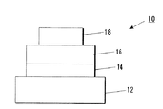
図1は、本発明の有機発光素子(OLED)10の例示的な実施形態を示している。有機発光素子10は、基板12、基板12上に位置する陽極14、陽極14上に位置する発光領域16及び発光領域16上に位置する陰極18からなる。動作中、電界を印加することによって正の電荷(正孔)及び負の電荷(電子)がそれぞれ陽極14及び陰極18から発光領域16へ注入されて再結合し、これによって発光領域16で発光が起きる。
【0022】
発光領域16は有機発光材料からなる。適切な有機発光材料を、例えば、金属オキシノイド化合物、スチルベン化合物、アントラシン化合物、オキサジアゾール金属キレート化合物、ポリフルオレン類、ポリフェニレンビニレン類、これらの誘導体及び混合物から選択することができる。他の適切な有機発光材料を以下に説明する。
【0023】
さらに発光領域16は、一つ以上の正孔輸送材料及び電子輸送材料からなる。
【0024】
さらに、以下に説明するように、有機発光素子10の実施形態は、陽極14と発光領域16との間の正孔輸送領域及び陰極18と発光領域16との間の電子輸送領域のうちの少なくとも一つを含むことができる。このような正孔輸送領域及び/又は電子輸送領域は、適切な正孔輸送材料として、例えば、ポリフェニレンビニレン類、ポリチオフェン類、第3芳香族アミン類、インドロカルバゾール化合物等の物質、並びに適切な電子輸送材料として、例えば、金属オキシノイド類、トリアジン類、オキサジアゾール金属キレート、スチルベン類、ポリフルオレン類等の物質からなることができる。
【0025】
本発明の有機発光素子100の他の例示的な実施形態を図2に示す。有機発光素子100は、基板112、基板112上に位置する陽極114、陽極114上に位置する発光領域116、発光領域116上に位置する陰極118からなる。この実施形態では、有機発光素子100は、陽極114上に位置し正孔輸送材料(HTM)からなる正孔輸送領域120及び正孔輸送領域120上に位置し陰極118に隣接する、電子輸送材料(ETM)からなる電子輸送領域122を含む。正孔輸送領域120及び電子輸送領域122のうちの少なくとも一方が、これら二つの領域の組成に応じて光を放出する。正孔輸送領域120及び電子輸送領域122を形成するのに適した材料を、例えば、上記に説明した材料から選択することができる。
【0026】
本発明の有機発光素子200の他の例示的な実施形態を図3に示す。有機発光素子200は、基板212、基板212上に位置する陽極214、陽極214上に位置する発光領域216、及び発光領域216上に位置する陰極218からなる。
【0027】
有機発光素子200では、発光領域216は、陽極214上に位置し正孔輸送材料からなる正孔輸送領域220、陰極218に隣接し電子輸送材料からなる電子輸送領域222及び正孔輸送領域220上に位置し正孔輸送材料と電子輸送材料との混合物からなる混合領域224からなる。
【0028】
有機発光素子200では、一般的に混合領域224が発光領域の発光部分である。したがって、このような実施形態では、正孔輸送材料及び電子輸送材料のうちの一方がエミッタとなる。他の実施形態では、混合領域224は発光ドープ材料をさらに含む。このような実施形態では、混合領域を形成する正孔輸送材料と電子輸送材料のうちの少なくとも一方がエミッタであってもよい。
【0029】
しかし、有機発光素子200の他の例示的な実施形態では、正孔輸送領域220及び電子輸送領域22のうち少なくとも一方によって発光が任意にもたらされ得ることが考えられる。さらに、有機発光素子200のまた他の実施形態では、正孔輸送領域220、混合領域224及び電子輸送領域222のうちの二つ以上によって発光がもたらされ得る。正孔輸送領域220、電子輸送領域222及び混合領域224を形成するのに適した材料を、例えば、上記に説明した材料から選択することができる。混合領域224が一つ以上の発光ドープ材料からなる実施形態では、適切な発光ドープ材料を、例えば、蛍光染料又はリン光材料から選択することができる。
【0030】
本発明の有機発光素子200の幾つかの例示的な実施形態では、正孔輸送領域220又は電子輸送領域222の一つだけが混合領域224に隣接して形成される。陽極214と混合領域224との間に正孔輸送領域220を含むが、混合領域224と陰極218との間に電子輸送領域222を含まない有機発光素子200の実施形態では、混合領域224は陰極218に接触する。このような実施形態では、正孔輸送領域220及び混合領域224のうち少なくとも一方がエミッタとなる。
【0031】
混合領域224と陰極218との間に電子輸送領域222を含むが陽極214と混合領域224との間に正孔輸送領域220を含まない有機発光素子200の他の実施形態では、混合領域224は陽極214に接触する。このような実施形態では、電子輸送領域222と混合領域224のうち少なくとも一方がエミッタとなる。
【0032】
本発明の有機発光素子の幾つかの例示的な実施形態では、混合領域224、正孔輸送領域220及び電子輸送領域222のうち少なくとも一つが複数の層からなる。有機発光素子10及び100に対しても多層構造体を形成することもできる。
【0033】
本発明によると、混合領域224の正孔輸送材料と正孔輸送領域220の正孔輸送材料は同じでもよいし、任意で異なる材料でもよい。同様に、混合領域224の電子輸送材料と電子輸送領域222の電子輸送材料は同じ材料でもよいし、任意で異なる材料でもよい。
【0034】
本発明の有機発光素子の他の例示的な実施形態は、基板、基板上に位置する陽極、陽極上に位置する発光領域、及び発光領域上に位置する陰極からなる。このような実施形態では、発光領域は、陽極上に位置し正孔輸送材料からなる正孔輸送領域、正孔輸送領域上に位置し有機発光材料からなる発光部分、発光部分上且つ陰極に隣接して位置し電子輸送材料からなる電子輸送領域からなる。したがって、本発明の有機発光素子のこのような実施形態の構造は、混合領域224が発光部分に代わったことを除いて、図3に示す有機発光素子200の構造に類似している。正孔輸送領域、発光部分及び電子輸送領域を形成するのに適した材料を、例えば、上記の材料から選択することができる。
【0035】
本発明の他の例示的な実施形態では、有機発光素子は、陽極ではなく陰極が基板に接触する素子構造からなることができる。このような有機発光素子300の例示的な実施形態を図4に示す。有機発光素子300は、基板312、基板312上に位置する陰極318、陰極318上に位置する発光領域316及び発光領域316上に位置する陽極314からなる。動作中、電界を印加することによって正電荷(正孔)及び負電荷(電子)がそれぞれ陽極314及び陰極318から発光領域316へ注入されて再結合し、発光領域316で発光する。
【0036】
発光領域316は、例えば、上述した図2における有機発光素子100の発光領域116又は有機発光素子200の発光領域216と同じ構造であってもよい。
【0037】
広範囲の波長の光を放出するように、有機発光素子の実施形態を製造することができる。発光材料、正孔輸送材料及び電子輸送材料の適切な組み合わせ及び混合物を選択することによって、約400nm〜約700nmの波長の光を有機発光素子から放出することができる。したがって、本発明の有機発光素子は、適切な材料を選択することによって広範囲にわたる異なる色の光を放出することができる。発光の色が多様であるために、赤、緑又は青のような幾つかの特定の色の光が所望される種々の用途で本発明の有機発光素子を使用することができる。
【0038】
種々の発光材料、正孔輸送材料及び電子輸送材料が当業界で公知であり、また、所望の色の発光を達成するための材料の組み合わせの選択も公知である。さらに、所望の色の発光を提供するためのこのような材料の選択は、当業者によって通常の実験で容易に実施できる。
【0039】
有機発光素子の実施形態を交流(AC)及び/又は直流(DC)駆動条件下で動作させることができる。以下に、より詳細に述べるように、動作寿命を長くするために幾つかの実施形態ではAC駆動条件が好ましい。
【0040】
本発明の有機発光素子の従来技術とは異なる部分をより詳細に説明する。
【0041】
基板12、112、212及び312は任意の適切な材料からなってよい。例えば、基板12、112、212及び312は、ポリマー成分、ガラス、石英などからなり得る。適切なポリマー成分として、マイラー(登録商標:MYLAR)のようなポリエステル類、ポリカーボネート類、ポリアクリレート類、ポリメタクリレート類、ポリスルホン類などが挙げられるが、これらに限定しない。これらの種々の材料の混合物を使用することもできる。例えば、その材料が他の層を有効に支持でき、素子の機能的な性能に干渉しないならば、他の基板の材料を選択することもできる。本実施形態では、基板12、112、212及び312は光透過材料から形成されるのが好ましい。
【0042】
基板12、112、212及び312の厚さは、有機発光素子の構造的な要求及びその意図する使用によって制限される以外、特に制限されない。基板は、一般的に例えば約25μm〜少なくとも約1000μmの厚さである。
【0043】
基板12、112、212及び発光領域316上に形成された陽極14、114、214及び314は、それぞれ任意の適切な公知の材料又はこれから開発される材料から構成することができる。例えば、酸化インジウム錫(ITO)、酸化錫、金及びプラチナのような正電荷注入電極を使用することができる。陽極に適した他の材料として、例えば、少なくとも約4eV、好ましくは約4eV〜約6eVの仕事関数の導電性炭素、π−共役ポリマー、例えば、ポリアニリン、ポリピロールなどが挙げられるが、これらに限定しない。
【0044】
陽極14、114、214及び314は任意の適切な構造をとることができる。薄い導電層を光透過性基板、例えば、透明又は実質的に透明なガラス板又はプラスチックフィルム上に被覆することができる。また、本発明の有機発光素子の実施形態においては、ガラス板の上に被覆され、酸化錫又は酸化インジウム錫(ITO)から形成された光透過性陽極として構成することもできる。例えば、約200Å未満、好ましくは約75Å〜約150Åの厚さの非常に薄い光透明金属陽極を使用することができる。これらの薄い陽極は、金、パラジウムなどのような金属からなることができる。さらに、導電性炭素又は上述の共役ポリマーからなる、例えば、50Å〜約175Åの厚さの透明又は半透明の薄い層を陽極として使用することもできる。陽極14、114、214及び314(以下により詳細に示すように、陰極18、118、218及び318)の他の適切な形態でも使用できる。
【0045】
陽極14、114、214及び314の厚さは約1nm〜約500nmで、好ましい厚さの範囲は陽極の材料の光学定数に依る。陽極の厚さの一つの好ましい範囲は、約30nm〜約300nmである。もちろん、この範囲外の厚さも使用できる。
【0046】
発光領域16、116、216、316は、有機発光材料を含む任意の適切な公知の又はこれから開発される一つ以上の材料からなることができる。発光領域16、116、216、316で利用できる適切な有機発光材料として、ポリフェニレンビニレン類、例えば、ポリ(p−フェニレンビニレン)(PPV)、ポリ(2−メトキシ−5−(2−エチルヘキシルオキシ)1,4−フェニレンビニレン)(MEHPPV)、ポリ(2,5−ジアルコキシフェニレンビニレン)(PDMeOPV)等の材料が挙げられる。
【0047】
発光領域16、116、216、316で利用できる他の適切な有機発光材料として、ポリフェニレン類、例えば、ポリ(p−フェニレン)(PPP)、ラダー−ポリ−パラ−フェニレン(LPPP)及びポリ(テトラヒドロピレン)(PTHP)等が挙げられる。
【0048】
発光領域16、116、216、316で利用できるさらに他の適切な例示的な有機発光材料として、ポリフルオレン類、例えばポリ(9,9−ジ−n−オクチルフルオレン−2,7−ジイル)、ポリ(2,8−(6,7,12,12−テトラアルキルインデノフルオレン)、また、例えば、ベルニウスら(Bernius et. al.)による"Proceedings of SPIE Conference on Organic Light Emitting Materials and Devices III", Denver, Colorado, July 1999, Vol. 3797, p.129に記載されたフルオレン−アミンコポリマー類のようなフルオレン類を含有するポリマー類も挙げられる。
【0049】
発光領域16、116、216、316で利用できる有機発光材料の好ましいクラスとして、金属オキシノイド化合物が挙げられるがこれに限定しない。例えば、一つの好ましい例として、トリス(8−ヒドロキシキノリネート)アルミニウム(Alq3)が挙げられ、別の好ましい例として、ビス(8−ヒドロキシキノラート)−(4−フェニルフェノラート)アルミニウム(BAlq)が挙げられる。このクラスの材料の他の例として、トリス(8−ヒドロキシキノリネート)ガリウム、ビス(8−ヒドロキシキノリネート)マグネシウム、ビス(8−ヒドロキシキノリネート)亜鉛、トリス(5−メチル−8−ヒドロキシキノリネート)アルミニウム、トリス(7−プロピル−8−キノリノラート)アルミニウム、ビス[ベンゾ{f}−8−キノリネート]亜鉛、ビス(10−ヒドロキシベンゾ[h]キノリネート)ベリリウムなどが挙げられ、さらに、金属チオキシノイド化合物、例えば、ビス(8−キノリンチオラート)亜鉛、ビス(8−キノリンチオラート)カドミウム、トリス(8−キノリンチオラート)ガリウム、トリス(8−キノリンチオラート)インジウム、ビス(5−メチルキノリンチオラート)亜鉛、トリス(5−メチルキノリンチオラート)ガリウム、トリス(5−メチルキノリンチオラート)インジウム、ビス(5−メチルキノリンチオラート)カドミウム、ビス(3−メチルキノリンチオラート)カドミウム、ビス(5−メチルキノリンチオラート)亜鉛、ビス[ベンゾ{f}−8−キノリンチオラート]亜鉛、ビス[3−メチルベンゾ{f}−8−キノリンチオラート]亜鉛、ビス[3,7−ジメチルベンゾ{f}−8−キノリンチオラート]亜鉛などの金属チオキシノイド化合物が挙げられる。好ましい材料は、ビス(8−キノリンチオラート)亜鉛、ビス(8−キノリンチオラート)カドミウム、トリス(8−キノリンチオラート)ガリウム、トリス(8−キノリンチオラート)インジウム及びビス[ベンゾ{f}−8−キノリンチオラート]亜鉛である。
【0050】
発光領域16、116、216、316で使用できる他の好ましいクラスの有機発光材料は、スチルベン誘導体を含む。好ましいスチルベン誘導体は、4,4’−ビス(2,2−ジフェニルビニル)ビフェニルである。
【0051】
発光領域16、116、216、316を形成するのに適した他のクラスの有機発光材料は、オキサジアゾール金属キレート類である。これらの材料として、ビス[2−(2−ヒドロキシフェニル)−5−フェニル−1,3,4−オキサジアゾラート]亜鉛、ビス[2−(2−ヒドロキシフェニル)−5−フェニル−1,3,4−オキサジアゾラート]ベリリウム、ビス[2−(2−ヒドロキシフェニル)−5−(1−ナフチル)−1,3,4−オキサジアゾラート]亜鉛、ビス[2−(2−ヒドロキシフェニル)−5−(1−ナフチル)−1,3,4−オキサジアゾラート]ベリリウム、ビス[5−ビフェニル−2−(2−ヒドロキシフェニル)−1,3,4−オキサジアゾラート]亜鉛、ビス[5−ビフェニル−2−(2−ヒドロキシフェニル)−1,3,4−オキサジアゾラート]ベリリウム、ビス[2−(2−ヒドロキシフェニル)−5−フェニル−1,3,4−オキサジアゾラート]リチウム、ビス[2−(2−ヒドロキシフェニル)−5−p−トリル−1,3,4−オキサジアゾラート]亜鉛、ビス[2−(2−ヒドロキシフェニル)−5−p−トリル−1,3,4−オキサジアゾラート]ベリリウム、ビス[5−(p−t−ブチルフェニル)−2−(2−ヒドロキシフェニル)−1,3,4−オキサジアゾラート]亜鉛、ビス[5−(p−t−ブチルフェニル)−2−(2−ヒドロキシフェニル−1,3,4−オキサジアゾラート]ベリリウム、ビス[2−(2−ヒドロキシフェニル)−5−(3−フルオロフェニル)−1,3,4−オキサジアゾラート]亜鉛、ビス[2−(2−ヒドロキシフェニル)−5−(4−フルオロフェニル)−1,3,4−オキサジアゾラート]亜鉛、ビス[2−(2−ヒドロキシフェニル)−5−(4−フルオロフェニル)−1,3,4−オキサジアゾラート]ベリリウム、ビス[5−(4−クロロフェニル)−2−(2−ヒドロキシフェニル)−1,3,4−オキサジアゾラート]亜鉛、ビス[2−(2−ヒドロキシフェニル)−5−(4−メトキシフェニル)−1,3,4−オキサジアゾラート]亜鉛、ビス[2−(2−ヒドロキシ−4−メチルフェニル)−5−フェニル−1,3,4−オキサジアゾラート]亜鉛、ビス[2−α−(2−ヒドロキシナフチル)−5−フェニル−1,3,4−オキサジアゾラート]亜鉛、ビス[2−(2−ヒドロキシフェニル)−5−p−ピリジル−1,3,4−オキサジアゾラート]亜鉛、ビス[2−(2−ヒドロキシフェニル)−5−p−ピリジル−1,3,4−オキサジアゾラート]ベリリウム、ビス[2−(2−ヒドロキシフェニル)−5−(2−チオフェニル)−1,3,4−オキサジアゾラート]亜鉛、ビス[2−(2−ヒドロキシフェニル)−5−フェニル−1,3,4−チアジアゾラート]亜鉛、ビス[2−(2−ヒドロキシフェニル)−5−フェニル−1,3,4−チアジアゾラート]ベリリウム、ビス[2−(2−ヒドロキシフェニル)−5−(1−ナフチル)−1,3,4−チアジアゾラート]亜鉛、ビス[2−(2−ヒドロキシフェニル)−5−(1−ナフチル)−1,3,4−チアジアゾラート]ベリリウムなどが挙げられる。
【0052】
発光領域16、116、216、316で利用できる他のクラスの適切な有機発光材料は、トリアジン類である。
【0053】
発光領域16、116、216、316で利用できる他のクラスの適切な有機発光材料は、アントラシン類である。
【0054】
発光領域16、116、216、316で利用できる有機発光材料の他の好ましい例として、蛍光材料、例えばクマリン、ジシアノメチレンピラン、ポリメチン、オキサベンズアントラン、キサンテン、ピリリウム、カルボスチル、ペリレンなどが挙げられる。他の特に好ましいクラスの蛍光材料は、キナクリドン染料である。キナクリドン染料の例として、キナクリドン、2−メチルキナクリドン、2,9−ジメチルキナクリドン、2−クロロキナクリドン、2−フルオロキナクリドン、1,2−ベンゾキナクリドン、N,N’−ジメチルキナクリドン、N,N’−ジメチル−2−メチルキナクリドン、N,N’−ジメチル−2,9−ジメチルキナクリドン、N,N’−ジメチル−2−クロロキナクリドン、N,N’−ジメチル−2−フルオロキナクリドン、N,N’−ジメチル−1,2−ベンゾキナクリドン、などが挙げられる。他の好ましいクラスの蛍光材料は、縮合環蛍光染料である。縮合環蛍光染料の例として、全体を参照として本明細書中に援用する米国特許第3,172,862号に示したようなペリレン、ルブレン、アントラセン、コロネン、フェナントレセン、ピレンなどが挙げられる。また、蛍光材料として、ブタジエン類、例えば、1,4−ジフェニルブタジエン及びテトラフェニルブタジエン、スチルベンなどが挙げられる。他の例示的な蛍光材料を使用することもできる。
【0055】
発光領域16、116、216、316で利用できる他の好ましいクラスの有機発光材料は蛍光染料である。例えば、4−(ジシアノメチレン)−2−I−プロピル−6−(1,1,7,7−テトラメチルユロリジル−9−エニル)−4H−ピラン(DCJTB)が挙げられる。
【0056】
発光領域16、116、216、316で利用できる他の好ましいクラスの有機発光材料は、ランタニド金属キレート錯体、例えば、キドら(Kido et. al.)による"White Light Emitting Organic Electroluminescent Device Using Lanthanide Complexes" Jpn.J.Appl.Phys., Vol. 35, pp. L394-L396 (1996)に記載されたような、トリス(アセチルアセトナート)(フェナントロリン)テルビウム、トリス(アセチルアセトナート)(フェナントロリン)ユーロピウム、トリス(テノイルトリスフルオロアセトナート)(フェナントロリン)ユーロピウムである。
【0057】
発光領域16、116、216、316で利用できる他の好ましいクラスの有機発光材料は、リン光材料、例えば、バルドら(Baldo et. al.)による”Hightly Efficient Organic Phosphorescent Emission from Organic ElectroluminescentDevices”, Letters to Nature, Vol. 395, pp. 151-154 (1998)に記載された化合物のような、強力なスピン軌道結合を誘導する重金属原子を含有する有機金属化合物である。好ましい例として、2,3,7,8,12,13,17,18−オクタエチル−21H23H−フォルピンプラチナ(II)(PtOEP)及びfacトリス(2−フェニルピリジン)イリジウム(Ir(ppy)3)が挙げられる。
【0058】
発光領域16、316、正孔輸送領域120、220及び混合領域224を形成するのに利用できる正孔輸送材料並びに発光領域16、316、電子輸送領域122、222及び混合領域224を形成するのに利用できる電子輸送材料は、任意の適切な公知の材料又はこれから開発される材料であってもよい。
【0059】
発光領域16、316、正孔輸送領域120、220及び混合領域224で利用できる例示的な正孔輸送材料として、ポリピロール、ポリアニリン、ポリ(フェニレンビニレン)、ポリチオフェン、ポリアリールアミン、これらの誘導体、公知の半導体有機材料、ポルフィリン誘導体、例えば、1,10,15,20−テトラフェニル−21H,23H−ポルフィリン銅(II)、銅フタロシアニン、銅テトラメチルフタロシアニン、亜鉛フタロシアニン、酸化チタンフタロシアニン、マグネシウムフタロシアニンなどが挙げられる。
【0060】
発光領域16、316、正孔輸送領域120、220及び混合領域224で利用できる好ましいクラスの正孔輸送材料は、芳香族第3アミン類である。芳香族第3アミン類の適切な例として、例えば、ビス(4−ジメチルアミノ−2−メチルフェニル)フェニルメタン、N,N,N−トリ(p−トリル)アミン、1,1−ビス(4−ジ−p−トリルアミノフェニル)シクロヘキサン、1,1−ビス(4−ジ−p−トリルアミノフェニル)−4−フェニルシクロヘキサン、N,N’−ジフェニル−N,N’−ビス(3−メチルフェニル)−1,1’−ビフェニル−4,4’−ジアミン、N,N’−ジフェニル−N,N’−ビス(3−メチルフェニル)−1,1’−ビフェニル−4,4’−ジアミン、N,N’−ジフェニル−N,N’−ビス(4−メトキシフェニル)−1,1’−ビフェニル−4,4’−ジアミン、N,N,N’,N’−テトラ−p−トリル−1,1’−ビフェニル−4,4’−ジアミン、N,N’−ジ−1−ナフチル−N,N’−ジフェニル−1,1’−ビフェニル−4−4’−ジアミン、これらの混合物などが挙げられる。
【0061】
発光領域16、316、正孔輸送領域120、220及び混合領域224で利用できる他のクラスの芳香族第3アミン類は、多核性芳香族アミン類である。このような多核性芳香族アミン類として、例えば、N,N−ビス−[4’−(N−フェニル−N−m−トリルアミノ)−4−ビフェニリル]アニリン、N,N−ビス−[4’−(N−フェニル−N−m−トリルアミノ)−4−ビフェニリル]−m−トルイジン、N,N−ビス−[4’−(N−フェニル−N−m−トリルアミノ)−4−ビフェニリル]−p−トルイジン、N,N−ビス−[4’−(N−フェニル−N−p−トリルアミノ)−4−ビフェニリル]アニリン、N,N−ビス−[4’−(N−フェニル−N−p−トリルアミノ)−4−ビフェニリル]−m−トルイジン、N,N−ビス−[4’−(N−フェニル−N−p−トリルアミノ)−4−ビフェニリル]−p−トルイジン、N,N−ビス−[4’−(N−フェニル−N−p−クロロフェニルアミノ)−4−ビフェニリル]−m−トルイジン、N,N−ビス−[4’−(N−フェニル−N−m−クロロフェニルアミノ)−4−ビフェニリル]−m−トルイジン、N,N−ビス−[4’−(N−フェニル−N−m−クロロフェニルアミノ)−4−ビフェニリル]−p−トルイジン、N,N−ビス−[4’−(N−フェニル−N−m−トリルアミノ)−4−ビフェニリル]−p−クロロアニリン、N,N−ビス−[4’−(N−フェニル−N−p−トリルアミノ)−4−ビフェニリル]−m−クロロアニリン、N,N−ビス−[4’−(N−フェニル−N−m−トリルアミノ)−4−ビフェニリル]−1−アミノナフタレン、これらの混合物などが挙げられる。
【0062】
発光領域16、316、正孔輸送領域120、220及び混合領域224で利用できる他のクラスの正孔輸送材料は、4,4’−ビス(9−カルバゾリル)−1,1’−ビフェニル化合物、例えば、4,4’−ビス(9−カルバゾリル)−1,1’−ビフェニル、4,4’−ビス(3−メチル−9−カルバゾリル)−1,1’−ビフェニルなどを含む。
【0063】
発光領域16、316、正孔輸送領域120、220及び混合領域224で利用できる好ましいクラスの正孔輸送材料は、インドロカラバゾール類である。
【0064】
発光領域16、316、正孔輸送領域120、220及び混合領域224で利用できる正孔輸送材料の他の好ましいクラスは、N,N,N’,N’−テトラアリールベンジジンからなり、アリールはフェニル、m−トリル、p−トリル、m−メトキシフェニル、p−メトキシフェニル、1−ナフチル、2−ナフチルなどから選択されてよい。N,N,N’,N’−テトラアリールベンジジンの例として、N,N’−ジ−1−ナフチル−N,N’−ジフェニル−1,1’−ビフェニル−4,4’−ジアミンがより好ましく、さらに、N,N’−ビス(3−メチルフェニル)−N,N’−ジフェニル−1,1’−ビフェニル−4−4’−ジアミン、N,N’−ビス(3−メトキシフェニル)−N,N’−ジフェニル−1,1’−ビフェニル−4,4’−ジアミンなどが挙げられる。
【0065】
発光領域16、316、正孔輸送領域120、220及び混合領域224で利用できる好ましい正孔輸送材料は、ナフチル置換ベンジジン誘導体である。
【0066】
発光領域16、316、電子輸送領域122、222及び混合領域224を形成するのに利用できる電子輸送材料の例を、金属オキシノイド化合物、オキサジアゾール金属キレート化合物、トリアジン化合物、スチルベン化合物から選択することができ、これらの例は上述されている。
【0067】
発光領域16、316、電子輸送領域122、222及び混合領域224を形成するのに利用できる電子輸送材料の他の例は、ポリフルオレン類、例えば、ポリ(9,9−ジ−n−オクチルフルオレン−2,7−ジイル)、ポリ(2,8−(6,7,12,12−テトラアルキルインデノフルオレン)及びフルオレンアミンコポリマーのようなフルオレンを含有するコポリマー類である。例えば、ベルニウスら(Bernius et. al.)による"Proceedings of SPIE Conference on Organic Light Emitting Materials and Devices III", Denver, Colorado, July 1999, Vol. 3797, p.129を参照のこと。
【0068】
本発明によると、混合領域224は、約10重量%〜約90重量%の正孔輸送材料と約90重量%〜約10重量%の電子輸送材料からなることができる。混合領域224は、約25重量%〜約75重量%の正孔輸送材料と約75重量%〜約25重量%の電子輸送材料からなることが好ましい。他の好ましい範囲は、約40重量%〜約60重量%の正孔輸送材料と約60重量%〜約40重量%の電子輸送材料である。
【0069】
本発明によると、実施形態では、混合領域は少なくとも一つの発光ドープ材料からなることができる。このような実施形態では、混合領域224は約10重量%〜約90重量%の正孔輸送材料、約90重量%〜約10重量%の電子輸送材料及び約0.1重量%〜約25重量%の発光ドープ材料からなることができる。混合領域224は、約25重量%〜約75重量%の正孔輸送材料、約75重量%〜約25重量%の電子輸送材料及び約0.1重量%〜約5重量%の発光ドープ材料からなるのが好ましい。
【0070】
上述した任意の適切な且つ例示的な正孔輸送材料と電子輸送材料との混合物を使用して、混合領域を形成することができる。
【0071】
任意の適切な公知の方法又はこれから開発される方法によって、上記の材料のうち一つを薄い層に形成することによって、発光領域16、116、216、316を含む一つ以上の層を調製することができる。この目的に適した方法として、例えば、蒸着及びスピンコーティング技術が挙げられる。
【0072】
発光領域16、116、216、316は、約10nm〜約1000nmの厚さを有し得る。この厚さは約50nm〜約250nmであるのが好ましい。発光領域が一つ以上の隣接する層からなる実施形態では、各層の厚さは少なくとも約5nmである。
【0073】
陰極18、118、218、318は、例えば、約4.0eV〜約6.0eVの仕事関数を有する高仕事関数成分、又は、例えば、約2.5eV〜約4.0eVの仕事関数の金属のような低仕事関数成分を含む任意の適切な金属からなることができる。陰極は、低仕事関数(約4eV未満)金属と、少なくとも一つの他の金属との組み合わせからなることができる。第2の即ち他の金属に対する低仕事関数金属の有効な割合は、約0.1重量%未満〜約99.9重量%である。低仕事関数金属の例として、アルカリ金属類、例えば、リチウム又はナトリウム、2A族即ちアルカリ土類金属、例えば、ベリリウム、マグネシウム、カルシウム又はバリウム、希土類金属及びアクチニド族金属を含むIII族の金属、例えば、スカンジウム、イットリウム、ランタン、セリウム、ユーロピウム、テルビウム又はアクチニウムが挙げられるが、これらに限定しない。リチウム、マグネシウム及びカルシウムが、好ましい低仕事関数金属である。
【0074】
米国特許第4,885,211号のMg−Ag合金の陰極は、一つの好ましい陰極の構造である。他の好ましい陰極の構造は米国特許第5,429,884号に記載されており、ここで陰極はアルミニウム及びインジウムのような他の高仕事関数金属とのリチウム合金から形成される。これらの特許全体を参照として本明細書中に援用する。
【0075】
陰極18、118、218、318の厚さは、例えば、約10nm〜約500nmの範囲であり得る。もちろん、この範囲外の厚さも使用できる。
【0076】
本発明の有機発光素子の処理方法の例示的な実施形態は、アニールする前の同じ素子の性能上の特性と比較してアニールした素子の性能上の特性を向上させるために、例示的な有機発光素子10、100、200又は300及び本発明によって形成された他の有機発光素子のうちの任意の一つをアニールすることからなる。
【0077】
本発明の有機発光素子の処理方法の例示的な実施形態は、例えば、例示的な有機発光素子10、100、200又は300のいずれかであり得る製造後の有機発光素子を提供することからなる。有機発光素子は、陽極、陰極及び陽極と陰極との間の発光領域からなる。発光領域は、上述の発光領域16、116、216、316の構造又は本発明によって形成した他の構造のうちのいずれか一つからなる。有機発光素子は、素子の性能上の特性を向上させるのに有効なアニール温度及び時間(アニール周期)でアニールされる。
【0078】
一般的に、有機発光素子は、アニール前に比べて動作電圧を下げエネルギー変換効率を上げるためにアニールされる。本発明の有機発光素子のアニール方法の例示的な実施形態では、製造後の有機発光素子をアニールすることによって、製造後の有機発光素子の動作電圧が少なくとも約10%低下する。アニールによって、製造後の素子の動作電圧を少なくとも約20%低下させるのが好ましく、少なくとも約30%低下させるのがより好ましい。
【0079】
動作電圧を低下させることによって、本発明の有機発光素子の電力消費も低下する。アニールした有機発光素子の電力消費は、アニールしていない素子に比べて少なくとも約10%低い。アニールによって、製造後の素子の電力消費が少なくとも約20%低下するのが好ましく、少なくとも約30%低下するのがより好ましい。
【0080】
有機発光素子のエネルギー変換効率は、素子への電力の入力に対する光出力の比として定義できる。本発明の有機発光素子のアニール方法の例示的な実施形態では、製造後の有機発光素子をアニールすることによって、製造後の有機発光素子のエネルギー変換効率が少なくとも約10%上昇する。アニールによって製造後の素子のエネルギー変換効率が少なくとも約25%上昇するのが好ましく、さらには、少なくとも約40%上昇するのがより好ましい。
【0081】
本発明の有機発光素子の処理方法の実施形態では、製造後の有機発光素子のアニールを、発光領域を形成する材料の溶解温度よりも低いアニール温度で実施する。アニール温度は、発光領域を形成する材料のうち少なくとも一つのガラス転移温度よりも低温であることが好ましい。アニール温度は、有機発光素子を形成する全ての材料のうち最も低いガラス転移温度を有する材料のガラス転移温度よりも低温であることがより好ましい。一般的には、アニール温度は、発光領域の組成に応じて約50℃〜約150℃である。アニール温度は、約60℃〜約100℃が好ましい。
【0082】
アニールの結果、有機発光素子の実質的な構造上の変化が起こらないように、アニール温度を選択するのも好ましい。例えば、実質的な構造上の変化とは、有機発光素子の異なる層の間、例えば、混合領域と混合領域に隣接する領域との間の物質の相互拡散である。また、アニールした素子の動作電圧がアニール前の素子の動作電圧よりも事実上高くならないように、アニール温度を選択する。
【0083】
有機発光素子の性能上の特性の所望の改良を十分に達成するように、有機発光素子のアニール時間を選択する。一般にアニール温度が上昇すると、所望の結果を得るためにアニール時間は短縮される。実施形態では、アニール時間は約0.1時間〜約100時間である。アニール時間は約0.25時間〜約25時間であることが好ましい。
【0084】
また、本発明は、異なる有機発光素子の互いに対する性能上の特性の均質性を向上させるために、複数の有機発光素子を処理する方法の例示的な実施形態も提供する。例えば、異なる有機発光素子の性能上の特性を互いに近づける、即ち性能上の特性をより均一かつ均質にするのに有効な温度及び時間で、二つ以上の有機発光素子をアニール処理する。
【0085】
幾つかの実施形態では、異なる有機発光素子が同じアニール室で同時にアニールされる。しかし、他の例示的な実施形態では、異なる有機発光素子を同じアニール室で異なる時間アニールすることもできるし、異なるアニール室でアニールすることもできる。このような前者及び後者の実施形態では、より均一な結果を導くために、異なる有機発光素子に使用するアニール条件は一般に同じアニール室でも異なるアニール室でもほぼ等しい。
【0086】
有機発光素子は任意の適切なアニール雰囲気でアニールされる。例えば、アニール雰囲気は、任意の適切なガス、例えば、窒素、アルゴン、ヘリウム、二酸化炭素もしくはこれらの混合物又は素子の性能に悪影響を及ぼさない任意の他の適切なガスを含み得る。他の適切なアニール環境は、湿度のない雰囲気、例えば、乾燥空気であり得る。アニール環境の他の例は、圧力が約10-2〜約10-10mmHgより低い、好ましくは約10-3〜約10-6mmHgより低い真空環境である。
【0087】
例えば、製造後の各有機発光素子の動作電圧に作用し、また製造後の各有機発光素子のエネルギー変換効率に作用して異なる有機発光素子の動作電圧及び/又はエネルギー変換効率が互いに近似する十数%未満だけ異なるように、二つ以上の有機発光素子をアニールすることができる。例えば、本実施形態では、異なる有機発光素子の動作電圧及び/又はエネルギー変換効率は、一般に約15%未満だけ異なる。異なる有機発光素子の動作電圧及び/又はエネルギー変換効率は、一般に約10%未満だけ異なるのが好ましい。
【0088】
加熱の速度(即ち、有機発光素子の温度が所望のアニール温度範囲まで上昇する速度)及び冷却の速度(即ち、アニール時間後に有機発光素子をアニール温度から所望のより低い温度、例えば周囲温度に冷却する速度)は、素子が割れたりショートしたりするような損傷を起こさないように十分に低いことが好ましい。有機発光素子の適切な加熱速度及び冷却速度は、例えば約0.5℃/分〜約20℃/分であり、約1℃/分〜約5℃/分が好ましい。
【0089】
【実施例】
本発明の種々の態様をさらに示すために以下の実施例を提供するが、これらは本発明の範囲を限定しようとするものではない。
【0090】
[実施例1]
実施例1は、有機発光素子の動作電圧を低下させることによってエネルギー変換効率を上昇させるアニールの効果を証明する。図3に示した構造を使用した。混合領域224は染料ドープ剤をさらに含んだ。ドープ材料を含有する混合領域を含む有機発光素子は、本明細書中に組み込まれた米国出願番号第09/606,670号に記載されている。ナフチル置換ベンジジン(NPB)、トリス(8−ヒドロキシキノリン)アルミニウム(ALQ3)及びジメチルキナクリドン(DMQ)を、正孔輸送領域220及び混合領域224の正孔輸送材料、電子輸送領域222及び混合領域224の電子輸送材料、混合領域224の染料ドープ剤にそれぞれ使用した。陽極214を酸化インジウム錫から形成し、陰極218をMg:Agから形成した。
【0091】
図5は、アニールの前後に測定した有機発光素子の電流密度対電圧特性を示す。アニールでは、素子を約90℃の温度で約20時間のアニール時間加熱した。アニール後の素子の電流密度対電圧特性がより低電圧にシフトしたことは、ある電流密度を駆動させるために(つまりある輝度を得るために)に必要な動作電圧が低下したことを証明している。
【0092】
図5に示すように、(ディスプレイに一般的な約250cd/m2の輝度を得るために)アニールした有機発光素子を約4mA/cm2の電流密度で動作させた場合、アニールの結果生じる電圧の低下は約40%であった。素子をこの輝度で動作させると、この電圧の低下によってエネルギー変換効率が約60%上昇した。
【0093】
[実施例2]
実施例2は、有機発光素子の動作電圧の低下、またエネルギー変換効率の上昇に関する製造後の有機発光素子のアニールの効果を証明する。実施例2では、有機発光素子は実施例1で使用したものと同じ一般的な構造であったが、混合領域224の染料ドープ剤としてDMQの代わりにナイルレッド染料を使用した。アニール条件は実施例1で使用したものと同一であった。実施例1に非常に類似した有機発光素子の特性の変化が実施例2で起こった。
【0094】
[実施例3]
実施例3は、有機発光素子の動作電圧を低下させエレクトロルミネセンス量子効率を上昇させ、またエネルギー変換効率を上昇させるアニールの効果を証明する。実施例3では正孔輸送領域220の正孔輸送材料が実施例1で使用したNPBの代わりにインドロカルバゾール化合物のみからなることを除いて、実施例3の有機発光素子の構造は実施例1と同様であった。
【0095】
100℃で24時間アニールした後、約5mA/cm2の電流密度を駆動させるために(約250cd/m2の輝度を得るために)必要な駆動電圧は約9%低下した。同時にこの電流密度で輝度は約10%上昇した(即ち、量子効率が約10%上昇した)。駆動電圧及びエレクトロルミネセンス効率両者の変化によって、素子の全体的なエネルギー変換効率がこの輝度レベルで約20%上昇した。
【0096】
[実施例4]
実施例4は、有機発光素子の動作電圧を低下させることによってエネルギー変換効率を上昇させるアニールの効果を証明する。図2に示す構造を有する有機発光素子を試験した。この素子では、インドロカルバゾール化合物及びトリス(8−ヒドロキシキノリン)アルミニウム(ALQ3)を、正孔輸送領域120の正孔輸送材料及び電子輸送領域122の電子輸送材料のそれぞれに使用した。陽極112を酸化インジウム錫から形成し、陰極118をMg:Agから形成した。
【0097】
素子を約100℃の温度で約24時間アニールした。アニールの結果、約5mA/cm2の電流密度を駆動させるために(約250cd/m2の輝度を得るために)必要な駆動電圧は約15%低下した。この動作電圧の低下は、この輝度レベルで有機発光素子のエネルギー変換効率が約17%上昇したことに対応する。
【0098】
[実施例5]
実施例5は、素子の性能をさらに向上させるためにアニール条件を制御することの重要性を証明する。実施例1で使用したものと同じ構造を有する有機発光素子を試験した。有機発光素子を約100℃の温度で約140時間アニールした。アニールの結果、約4mA/cm2の電流密度を駆動させるために(約250cd/m2の輝度を得るために)必要な駆動電圧は約20%上昇した。この上昇は、有機発光素子のエネルギー変換効率が約17%低下したことに対応する。
【0099】
この結果に基づくと、温度及び/又はアニール時間を適切に選択しないと、製造後の有機発光素子のアニール工程が素子の性能に悪影響を及ぼし得ることが明らかになった。
【0100】
[実施例6]
実施例6は、複数の異なる有機発光素子の素子性能を「均質化」するために熱アニールを使用することを証明する。各々が実施例1で上述した構造を有する三つの異なる素子A、B及びCを試験した。三つの素子の各々を、同じ製造工程のパラメータを使用して別の真空操業で製造した。製造後の状態の素子の評価は、三つの素子の特性にばらつきが見られた。特に、A、B及びCの素子のエネルギー変換効率はそれぞれ約3、3.4及び3.6ルーメン/ワットであった。素子の特性のばらつきは、平均値の3.33ルーメン/ワットから約±9%であった。このばらつきのレベルは有機発光素子では一般的であり、製造工程の条件(例えば、真空レベル、汚染物質レベル、蒸着速度など)の避けることのできないわずかな差によるものである。素子をまとめて約100℃で約24時間アニールした後、平均エネルギー変換効率は約4.9ルーメン/ワットに上昇し、平均値からのばらつきは約±3%になった。したがって、実施例6では、素子を本発明の方法でアニールすることによって、異なる有機発光素子の性能上の特性をより均一にできることが分かった。
【0101】
本発明のアニールした有機発光素子の性能上の特性が上述のように向上したことによって、アニールした有機発光素子を使用する種々のデバイスの性能を向上させることができる。したがって、本発明のアニールした有機発光素子を、向上した性能上の特性から利益を得る種々の用途で使用することができる。
【0102】
例えば、アニールした有機発光素子のエネルギー変換効率が上昇することで一つ以上のアニールした有機発光素子を含むディスプレイの電力消費を減少させることができる。さらに、アニールした有機発光素子のエネルギー変換効率が高いことは、熱の形態の電力の損失が減少し、アニールした有機発光素子を含む素子の過熱が減少することにも関連する。また、本発明のアニールした有機発光素子によって、所与の駆動電流での輝度を上昇させることもできる。例えば、本発明の有機発光素子を種々のディスプレイで使用してディスプレイの性能を向上させることができる。
【0103】
さらに、複数の異なる有機発光素子の性能上の特性を、本発明の方法の実施形態によって均質化することによって、重要な利益を得る。即ち、アニールの結果、互いにより一貫した特性を有する複数の有機発光素子を形成することができる。例えば、複数の素子が一定のエネルギー変換効率を有することができ、これによって素子の性能上の均一性が重要な用途で素子を使用することができる。より均一な性能を有する有機発光素子をディスプレイのようなデバイスで使用することができ、ディスプレイにより一貫した性能を提供することができる。さらに、本発明の有機発光素子を異なるデバイス例えば異なるディスプレイで使用して異なるディスプレイ間により一貫した性能を達成することができる。
【0104】
本発明の有機発光素子を種々の技術的な用途で使用することができる。例えば、上述のディスプレイのように発光素子を利用する種々の異なるタイプのデバイスで素子を使用することができる。例えば、ディスプレイは自動車のような車両にあってもよいし、コンピュータのモニター、テレビ並びに他の電子デバイス及びシステムにあってもよい。
【図面の簡単な説明】
【図1】本発明の有機発光素子の例示的な実施形態を例示する図である。
【図2】本発明の有機発光素子の他の例示的な実施形態を例示する図である。
【図3】本発明の有機発光素子のさらに他の例示的な実施形態を例示する図である。
【図4】本発明の有機発光素子のさらに他の例示的な実施形態を例示する図である。
【図5】有機発光素子のアニールの前後に測定した、有機発光素子の電流密度対電圧特性を示すグラフである。
【符号の説明】
10、100、200、300 有機発光素子
14、114、214、314 陽極
16、116、216、316 発光領域
18、118、218、318 陰極[0001]
BACKGROUND OF THE INVENTION
The present invention relates to optoelectronic devices, and more particularly to organic light emitting devices. The present invention further relates to a method for annealing an organic light emitting device.
[0002]
[Prior art]
Efficient electroluminescence from bilayer organic devices has been reported. Since that time, organic light emitting devices (OLEDs) have received much attention due to the possibility of producing large area displays.
[0003]
As explained in the article by Sheats et al., The basic structure of an organic light emitting device consists of two electrodes and an organic material between these electrodes. Electrons have a low work functionofHoles are injected into the organic material from the cathode and holes are high work functionofInjected into the organic material from the anode. Holes and electrons combine with an organic material to form a luminescent excited state.
[0004]
Organic light emitting devices (OLEDs) present a promising technology for various applications. These devices offer important advantages including a variety of luminescent colors, high energy conversion efficiency, and relatively low operating voltage. Organic light emitting devices can generate light with a luminance of the level of 100 cd / cm @ 2 at an operating voltage generally less than 10 volts.
[0005]
[Problems to be solved by the invention]
Publicly knownAccording to conventional technologyWhile organic light emitting devices can provide the above advantages, there is still a need to further reduce the operating voltage of the device without reducing quantum efficiency. The quantum efficiency of an organic light emitting device can be defined as the number of emitted photons per charge carried to the device. A decrease in operating voltage that is not accompanied by a decrease in quantum efficiency directly leads to an increase in energy conversion efficiency and a decrease in power consumption of elements including organic light emitting elements. High energy conversion efficiency results in low power loss in the form of heat generation and therefore less element overheating.
[0006]
[Means for Solving the Problems]
The present invention provides an organic light emitting device that can meet at least some of the above and other needs. In an exemplary embodiment of the organic light emitting device of the present invention, the operating voltage is reduced. Furthermore, in the exemplary embodiment of the organic light emitting device of the present invention, the energy conversion efficiency is increased.
[0007]
The organic light emitting device of the present invention comprises an annealed organic light emitting device after manufacture. The annealed organic light emitting device of the present invention comprises an anode, a cathode, and a light emitting region between the anode and the cathode. The light emitting region is made of an organic light emitting material.
[0008]
The embodiment of the organic light emitting device of the present invention may also include a hole transport region and / or an electron transport region adjacent to the light emitting region.
[0009]
The annealed organic light emitting device of the present invention has improved performance characteristics as compared to before annealing. In particular, in the annealed organic light emitting device, the operating voltage is lowered, but the quantum efficiency is not lowered. Therefore, the energy conversion efficiency of the annealed organic light emitting device is increased.
[0010]
In an exemplary embodiment of the annealed organic light emitting device of the present invention, high brightness levels of light can be emitted at a given drive current.
[0011]
The present invention also provides a method for annealing an organic light emitting device. An exemplary embodiment of this method is a temperature and time effective to improve the performance characteristics of an organic light emitting device.soHeating the element.
[0012]
In the exemplary embodiment of the method for annealing an organic light emitting device of the present invention, the operating voltage of the organic light emitting device can be reduced and the energy conversion efficiency can be improved as compared with the same characteristics before annealing.
[0013]
In some exemplary embodiments of the method for annealing an organic light emitting device of the present invention, an organic light emitting device with improved brightness at a given drive current can be obtained by annealing.
[0014]
The present invention further provides a method for annealing a plurality of organic light emitting devices, each of which may have different properties, such that the properties of the different devices are more uniform, ie, homogeneous. In order to provide more consistent device performance, annealed elements with more homogeneous characteristics can be used for the same device or optionally different devices.
[0015]
DETAILED DESCRIPTION OF THE INVENTION
Preferred embodiments of the present inventionAboutThis will be described in detail with reference to the drawings.
[0016]
The present invention provides an organic light emitting device (OLED) with improved performance. The present invention also provides a method for annealing an organic light emitting device to improve performance characteristics of the organic light emitting device.
[0017]
In an exemplary embodiment of the annealed organic light emitting device of the present invention, the operating voltage is reduced and the energy conversion efficiency is increased.
[0018]
An exemplary embodiment of the light emitting device of the present invention comprises an anode, a cathode, and a light emitting region between the anode and the cathode. The light emitting region may consist of a wide range of different organic light emitting materials.
[0019]
The organic light emitting device of the present invention is formed by annealing the manufactured organic light emitting device. As a result of the annealing, the characteristics and performance characteristics of the device can be remarkably improved as compared with the characteristics and performance characteristics of the device before annealing.
[0020]
In another exemplary embodiment of the method for annealing an organic light emitting device of the present invention, an annealed organic light emitting device having more uniform characteristics and performance characteristics than the characteristics and performance characteristics of each element is formed. be able to.
[0021]
FIG. 1 illustrates an exemplary embodiment of an organic light emitting device (OLED) 10 of the present invention.is doing. The organic
[0022]
The
[0023]
Further, the
[0024]
Further, as described below, the embodiment of the organic
[0025]
Another exemplary embodiment of the organic
[0026]
Another exemplary embodiment of the organic
[0027]
In the organic
[0028]
In the organic
[0029]
However, in other exemplary embodiments of the organic
[0030]
In some exemplary embodiments of the organic
[0031]
In another embodiment of the organic
[0032]
In some exemplary embodiments of the organic light emitting device of the present invention, at least one of the
[0033]
According to the present invention, the hole transport material in the
[0034]
Another exemplary embodiment of the organic light emitting device of the present invention comprises a substrate, an anode located on the substrate, a light emitting region located on the anode, and a cathode located on the light emitting region. In such an embodiment, the light emitting region is located on the anode and made of a hole transport material made of a hole transport material, the light emitting portion made of an organic light emitting material located on the hole transport region, on the light emitting portion and adjacent to the cathode. And an electron transport region made of an electron transport material. Therefore, the structure of such an embodiment of the organic light emitting device of the present invention is similar to the structure of the organic
[0035]
In another exemplary embodiment of the present invention, the organic light emitting device may be composed of a device structure in which the cathode contacts the substrate instead of the anode. An exemplary embodiment of such an organic
[0036]
The
[0037]
Embodiments of organic light emitting devices can be manufactured to emit a wide range of wavelengths of light. By selecting an appropriate combination and mixture of a light emitting material, a hole transport material, and an electron transport material, light having a wavelength of about 400 nm to about 700 nm can be emitted from the organic light emitting device. Therefore, the organic light emitting device of the present invention can emit a wide range of different colors by selecting an appropriate material. Because of the variety of colors of light emission, the organic light emitting devices of the present invention can be used in a variety of applications where some specific color light is desired, such as red, green or blue.
[0038]
Various light emitting materials, hole transport materials and electron transport materials are known in the art, and the selection of material combinations to achieve the desired color emission is also known. Furthermore, the selection of such materials to provide the desired color emission can be readily performed by those skilled in the art through routine experimentation.
[0039]
Embodiments of organic light emitting devices operate under alternating current (AC) and / or direct current (DC) drive conditionsProductCan be made. less than,As described in more detail,ProductIn some embodiments, AC drive conditions are preferred to increase life.
[0040]
The organic light emitting device of the present inventionWhat is conventional technology?The different parts will be described in more detail.
[0041]
The
[0042]
The thickness of the
[0043]
The
[0044]
The
[0045]
The thickness of the
[0046]
The
[0047]
Other suitable organic light emitting materials that can be used in the
[0048]
Still other suitable organic light emitting materials that can be utilized in the
[0049]
A preferred class of organic light emitting materials that can be used in the
[0050]
Another preferred class of organic light emitting materials that can be used in the
[0051]
Another class of organic light emitting materials suitable for forming the
[0052]
Another class of suitable organic light emitting materials that can be utilized in the
[0053]
Other classes of suitable organic light emitting materials that can be utilized in the
[0054]
Other preferred examples of organic light emitting materials that can be used in the
[0055]
Another preferred class of organic light emitting materials that can be utilized in the
[0056]
Another preferred class of organic light emitting materials that can be utilized in the
[0057]
Other preferred classes of organic light emitting materials that can be utilized in the
[0058]
A hole transport material that can be used to form the
[0059]
Exemplary hole transport materials that can be used in the
[0060]
A preferred class of hole transport materials that can be utilized in the
[0061]
Another class of aromatic tertiary amines that can be utilized in the
[0062]
Other classes of hole transport materials that can be utilized in the
[0063]
A preferred class of hole transport materials that can be utilized in the
[0064]
Other preferred classes of hole transport materials that can be utilized in the
[0065]
A preferred hole transport material that can be used in the
[0066]
Examples of electron transport materials that can be used to form the
[0067]
Other examples of electron transport materials that can be used to form the
[0068]
According to the present invention, the mixing
[0069]
According to the invention, in an embodiment, the mixed region can consist of at least one light emitting doped material. In such an embodiment, the mixing
[0070]
Any suitable and exemplary mixture of hole and electron transport materials described above can be used to form the mixed region.
[0071]
One or more layers including the
[0072]
The
[0073]
The
[0074]
The cathode of the Mg-Ag alloy of US Pat. No. 4,885,211 is one preferred cathode structure. Another preferred cathode structure is described in US Pat. No. 5,429,884, where the cathode is formed from a lithium alloy with other high work function metals such as aluminum and indium. These patents are incorporated herein by reference in their entirety.
[0075]
The thickness of the
[0076]
An exemplary embodiment of a method for treating an organic light emitting device of the present invention provides an exemplary organic method for improving the performance characteristics of an annealed device as compared to the performance properties of the same device prior to annealing. It comprises annealing any one of the
[0077]
Exemplary embodiments of the processing method of the organic light emitting device of the present invention include, for example,,It consists in providing a post-manufactured organic light emitting device which can be any of the exemplary organic
[0078]
In general, the organic light emitting device is annealed to lower the operating voltage and increase the energy conversion efficiency compared to before annealing. In an exemplary embodiment of the organic light emitting device annealing method of the present invention, annealing the manufactured organic light emitting device reduces the operating voltage of the manufactured organic light emitting device by at least about 10%. The annealing preferably reduces the operating voltage of the fabricated device by at least about 20%, and more preferably by at least about 30%.
[0079]
By reducing the operating voltage, the power consumption of the organic light emitting device of the present invention is also reduced. The power consumption of the annealed organic light emitting device is at least about 10% lower than that of the non-annealed device. Annealing preferably reduces the power consumption of the fabricated device by at least about 20%, and more preferably by at least about 30%.
[0080]
The energy conversion efficiency of an organic light emitting device can be defined as the ratio of the light output to the power input to the device. In an exemplary embodiment of the method for annealing an organic light emitting device of the present invention, annealing the manufactured organic light emitting device increases the energy conversion efficiency of the manufactured organic light emitting device by at least about 10%. Preferably, the annealing increases the energy conversion efficiency of the fabricated device by at least about 25%,Moreover,More preferably, it is increased by at least about 40%.
[0081]
In the embodiment of the processing method of the organic light emitting device of the present invention, annealing of the organic light emitting device after manufacture is performed at an annealing temperature lower than the melting temperature of the material forming the light emitting region. The annealing temperature is preferably lower than at least one glass transition temperature of the material forming the light emitting region. The annealing temperature is more preferably lower than the glass transition temperature of the material having the lowest glass transition temperature among all the materials forming the organic light emitting device. Generally, the annealing temperature is about 50 ° C. to about 150 ° C. depending on the composition of the light emitting region. The annealing temperature is preferably about 60 ° C to about 100 ° C.
[0082]
It is also preferable to select the annealing temperature so that the substantial structural change of the organic light emitting device does not occur as a result of the annealing. For example, a substantial structural change is between different layers of an organic light emitting device, for example,This is the interdiffusion of substances between the mixing region and the region adjacent to the mixing region. Also, the annealing temperature is selected so that the operating voltage of the annealed element is not substantially higher than the operating voltage of the element before annealing.
[0083]
The annealing time of the organic light emitting device is selected so as to sufficiently achieve the desired improvement in performance characteristics of the organic light emitting device. In general, as the annealing temperature increases, the annealing time is shortened to obtain the desired result. In embodiments, the annealing time is about 0.1 hours to about 100 hours. The annealing time is preferably about 0.25 hours to about 25 hours.
[0084]
The present invention also provides an exemplary embodiment of a method for processing a plurality of organic light emitting devices to improve the homogeneity of performance characteristics of different organic light emitting devices with respect to each other. For example, the performance characteristics of different organic light emitting devices are brought closer to each other, that is, the performance characteristics are more uniform.AndEffective temperature and time for homogenizationsoTwo or more organic light emitting devices are annealed.
[0085]
In some embodiments, different organic light emitting devices are annealed simultaneously in the same annealing chamber. However, in other exemplary embodiments, different organic light emitting devices can be annealed in the same annealing chamber for different times or in different annealing chambers. In these former and latter embodiments, the annealing conditions used for different organic light emitting devices are generally about the same in the same annealing chamber and in different annealing chambers in order to lead to more uniform results.
[0086]
The organic light emitting device is annealed in any suitable annealing atmosphere. For example, the annealing atmosphere can be any suitable gas, such as,Nitrogen, argon, helium, carbon dioxide or mixtures thereof or any other suitable gas that does not adversely affect the performance of the device may be included. Other suitable annealing environments are non-humid atmospheres, such as,It can be dry air. Another example of an annealing environment is a pressure of about 10-2~ About 10-Tenless than mmHg, preferably about 10-3~ About 10-6The vacuum environment is lower than mmHg.
[0087]
For example, the operating voltage and / or energy conversion efficiency of different organic light-emitting elements may be approximated to each other by acting on the operating voltage of each organic light-emitting element after manufacture and on the energy conversion efficiency of each organic light-emitting element after manufacture. Two or more organic light emitting devices can be annealed so as to differ by less than a few percent. For example,BookIn an embodiment, the operating voltage and / or energy conversion efficiency of different organic light emitting devices is,Generally differ by less than about 15%. It is generally preferred that the operating voltage and / or energy conversion efficiency of different organic light emitting devices differ by less than about 10%.
[0088]
The rate of heating (ie, the rate at which the temperature of the organic light emitting device rises to the desired annealing temperature range) and the rate of cooling (ie, cooling the organic light emitting device from the annealing temperature to the desired lower temperature, eg, ambient temperature after the annealing time) It is preferable that the speed of the operation is sufficiently low so as not to cause damage such as cracking or short-circuiting of the element. Suitable heating and cooling rates for the organic light emitting device are, for example, from about 0.5 ° C./min to about 20 ° C./min, preferably from about 1 ° C./min to about 5 ° C./min.
[0089]
【Example】
The following examples are provided to further illustrate various aspects of the present invention, but are not intended to limit the scope of the invention.
[0090]
[Example 1]
Example 1 demonstrates the effect of annealing to increase energy conversion efficiency by lowering the operating voltage of the organic light emitting device. The structure shown in FIG. 3 was used. The mixing
[0091]
FIG. 5 shows current density vs. voltage characteristics of the organic light emitting device measured before and after annealing. In the annealing, the device was heated at a temperature of about 90 ° C. for an annealing time of about 20 hours. The fact that the current density vs. voltage characteristics of the device after annealing has shifted to a lower voltage proves that the operating voltage required to drive a certain current density (that is, to obtain a certain luminance) has decreased. Yes.
[0092]
As shown in FIG. 5, the annealed organic light emitting device is operated at a current density of about 4 mA / cm 2 (to obtain a luminance of about 250 cd / m 2, which is typical for displays).ProductWhen this was done, the voltage drop resulting from annealing was about 40%. Move the element at this brightnessProductAs a result, the energy conversion efficiency increased by about 60% due to the decrease in voltage.
[0093]
[Example 2]
Example 2 proves the effect of annealing the organic light-emitting device after manufacture with respect to lowering the operating voltage of the organic light-emitting device and increasing the energy conversion efficiency. In Example 2, the organic light emitting device had the same general structure as that used in Example 1, but Nile Red dye was used instead of DMQ as the dye dopant in the
[0094]
[Example 3]
Example 3 demonstrates the effect of annealing to reduce the operating voltage of the organic light emitting device, increase the electroluminescence quantum efficiency, and increase the energy conversion efficiency. In Example 3, the structure of the organic light emitting device of Example 3 is the same as that of Example 1 except that the hole transport material in the
[0095]
After annealing for 24 hours at 100 ° C., the drive voltage required to drive a current density of about 5 mA / cm 2 (to obtain a brightness of about 250 cd / m 2) was reduced by about 9%. At the same time, the brightness increased by about 10% at this current density (ie, the quantum efficiency increased by about 10%). Changes in both drive voltage and electroluminescence efficiency increased the overall energy conversion efficiency of the device by about 20% at this brightness level.
[0096]
[Example 4]
Example 4 demonstrates the effect of annealing to increase energy conversion efficiency by reducing the operating voltage of the organic light emitting device. An organic light emitting device having the structure shown in FIG. 2 was tested. In this device, an indolocarbazole compound and tris (8-hydroxyquinoline) aluminum (ALQ3) were used for the hole transport material in the
[0097]
The device was annealed at a temperature of about 100 ° C. for about 24 hours. As a result of the annealing, the drive voltage required to drive a current density of about 5 mA / cm 2 (to obtain a brightness of about 250 cd / m 2) was reduced by about 15%. This decrease in operating voltage corresponds to an increase in energy conversion efficiency of the organic light emitting device of about 17% at this luminance level.
[0098]
[Example 5]
Example 5 demonstrates the importance of controlling annealing conditions to further improve device performance. An organic light emitting device having the same structure as that used in Example 1 was tested. The organic light emitting device was annealed at a temperature of about 100 ° C. for about 140 hours. As a result of the annealing, the drive voltage required to drive a current density of about 4 mA / cm 2 (to obtain a brightness of about 250 cd / m 2) increased by about 20%. This increase corresponds to a decrease of about 17% in the energy conversion efficiency of the organic light emitting device.
[0099]
Based on this result, it became clear that if the temperature and / or annealing time is not properly selected, the annealing process of the organic light-emitting device after manufacture can adversely affect the performance of the device.
[0100]
[Example 6]
Example 6 demonstrates the use of thermal annealing to “homogenize” the device performance of multiple different organic light emitting devices. Three different devices A, B and C, each having the structure described above in Example 1, were tested. Each of the three devices was manufactured in a separate vacuum operation using the same manufacturing process parameters. In the evaluation of the element in the state after manufacture, variations in the characteristics of the three elements were observed. In particular, the energy conversion efficiencies of the A, B, and C devices were about 3, 3.4, and 3.6 lumens / watt, respectively. The variation in device characteristics was about ± 9% from the average value of 3.33 lumens / watt. This level of variation is common in organic light emitting devices and is due to unavoidable slight differences in manufacturing process conditions (eg, vacuum level, contaminant level, deposition rate, etc.). After the devices were collectively annealed at about 100 ° C. for about 24 hours, the average energy conversion efficiency increased to about 4.9 lumens / watt, and the variation from the average value was about ± 3%. Therefore, in Example 6, it was found that the performance characteristics of different organic light emitting devices can be made more uniform by annealing the device by the method of the present invention.
[0101]
Since the performance characteristics of the annealed organic light emitting device of the present invention are improved as described above, the performance of various devices using the annealed organic light emitting device can be improved. Accordingly, the annealed organic light emitting devices of the present invention can be used in a variety of applications that benefit from improved performance characteristics.
[0102]
For example, increasing the energy conversion efficiency of the annealed organic light emitting device can reduce the power consumption of a display including one or more annealed organic light emitting devices. Furthermore, the high energy conversion efficiency of the annealed organic light emitting device is also related to a reduction in power loss in the form of heat and a decrease in overheating of the device including the annealed organic light emitting device. Also, the annealed organic light emitting device of the present invention can increase the brightness at a given drive current. For example, the organic light emitting device of the present invention can be used in various displays to improve display performance.
[0103]
In addition, significant benefits are gained by homogenizing the performance characteristics of a plurality of different organic light emitting devices through the method embodiments of the present invention. That is, as a result of annealing, a plurality of organic light emitting devices having more consistent characteristics can be formed. For example, a plurality of elements can have a constant energy conversion efficiency, which allows the elements to be used in applications where element performance uniformity is important. Organic light emitting devices with more uniform performance can be used in devices such as displays, and the displays can provide more consistent performance. Furthermore, the organic light emitting devices of the present invention can be used in different devices, such as different displays, to achieve more consistent performance between different displays.
[0104]
The organic light emitting device of the present invention can be used in various technical applications. For example, the elements can be used in a variety of different types of devices that utilize light emitting elements, such as the display described above. For example, the display may be in a vehicle such as a car, or in a computer monitor, television, and other electronic devices and systems.
[Brief description of the drawings]
FIG. 1 illustrates an exemplary embodiment of an organic light emitting device of the present invention.
FIG. 2 is a diagram illustrating another exemplary embodiment of the organic light emitting device of the present invention.
FIG. 3 is a view illustrating still another exemplary embodiment of the organic light emitting device of the present invention.
FIG. 4 is a diagram illustrating still another exemplary embodiment of the organic light emitting device of the present invention.
FIG. 5 is a graph showing current density vs. voltage characteristics of an organic light emitting device, measured before and after annealing of the organic light emitting device.
[Explanation of symbols]
10, 100, 200, 300 Organic light emitting device
14, 114, 214, 314 Anode
16, 116, 216, 316 Light emitting area
18, 118, 218, 318 Cathode
Claims (1)
陰極と、
前記陽極と前記陰極との間に配置され有機発光材料を含む発光領域と、を含む有機発光素子の製造方法において、前記有機発光素子の製造方法が、10−3〜10−6mmHgより低い圧力、90℃のアニール温度及び20時間のアニール時間、又は、100℃のアニール温度及び24時間のアニール時間でアニールされた状態にする工程を有し、
前記発光領域は、
正孔輸送材料を含み、前記陽極に隣接する正孔輸送領域と、
電子輸送材料を含み、前記陰極に隣接する電子輸送領域と、
前記正孔輸送材料、前記電子輸送材料及びドーパントの混合物を含む混合領を含み、
前記正孔輸送材料は、ナフチル置換ベンジジン又はインドロカルバゾール化合物であり、
前記電子輸送材料は、トリス(8−ヒドロキシキノリン)アルミニウムであり、
前記ドーパントは、ジメチルキナクリドンである
ことを特徴とする有機発光素子の製造方法。The anode,
A cathode,
In the manufacturing method of an organic light emitting device including a light emitting region including an organic light emitting material is disposed between the anode and the cathode, the manufacturing method of the organic light emitting device, a pressure below 10 -3 to 10 -6 mmHg , 90 ° C. annealing temperature and 20 hours annealing time of, or has a step of the annealed condition at 100 ° C. annealing temperature and 24 hours annealing time of,
The light emitting region is
A hole transport region comprising a hole transport material and adjacent to the anode;
An electron transport region comprising an electron transport material and adjacent to the cathode;
Comprising a mixture comprising the hole transport material, the electron transport material and a mixture of dopants,
The hole transport material is a naphthyl-substituted benzidine or indolocarbazole compound,
The electron transport material is tris (8-hydroxyquinoline) aluminum;
The method for manufacturing an organic light-emitting device, wherein the dopant is dimethylquinacridone.
Applications Claiming Priority (2)
| Application Number | Priority Date | Filing Date | Title |
|---|---|---|---|
| US629163 | 2000-07-31 | ||
| US09/629,163 US6734623B1 (en) | 2000-07-31 | 2000-07-31 | Annealed organic light emitting devices and method of annealing organic light emitting devices |
Publications (3)
| Publication Number | Publication Date |
|---|---|
| JP2002100473A JP2002100473A (en) | 2002-04-05 |
| JP2002100473A5 JP2002100473A5 (en) | 2007-09-27 |
| JP4657512B2 true JP4657512B2 (en) | 2011-03-23 |
Family
ID=24521857
Family Applications (1)
| Application Number | Title | Priority Date | Filing Date |
|---|---|---|---|
| JP2001217393A Expired - Lifetime JP4657512B2 (en) | 2000-07-31 | 2001-07-18 | Organic light emitting device |
Country Status (3)
| Country | Link |
|---|---|
| US (2) | US6734623B1 (en) |
| EP (1) | EP1178546B1 (en) |
| JP (1) | JP4657512B2 (en) |
Families Citing this family (35)
| Publication number | Priority date | Publication date | Assignee | Title |
|---|---|---|---|---|
| US6803720B2 (en) * | 2000-12-15 | 2004-10-12 | Universal Display Corporation | Highly stable and efficient OLEDs with a phosphorescent-doped mixed layer architecture |
| SG115435A1 (en) * | 2000-12-28 | 2005-10-28 | Semiconductor Energy Lab | Luminescent device |
| TW518909B (en) * | 2001-01-17 | 2003-01-21 | Semiconductor Energy Lab | Luminescent device and method of manufacturing same |
| CN101916829B (en) * | 2001-06-15 | 2012-05-09 | 佳能株式会社 | Organic electroluminescent device |
| JP2003059657A (en) * | 2001-08-10 | 2003-02-28 | Sumitomo Chem Co Ltd | Manufacturing method of organic electroluminescence element |
| US20030054197A1 (en) * | 2001-09-20 | 2003-03-20 | Raymond Kwong | Annealing modified interface in organic light emitting devices |
| US6759146B2 (en) * | 2001-11-08 | 2004-07-06 | Xerox Corporation | Organic devices |
| US6931132B2 (en) * | 2002-05-10 | 2005-08-16 | Harris Corporation | Secure wireless local or metropolitan area network and related methods |
| US6784017B2 (en) * | 2002-08-12 | 2004-08-31 | Precision Dynamics Corporation | Method of creating a high performance organic semiconductor device |
| TW554641B (en) * | 2002-08-19 | 2003-09-21 | Univ Nat Taiwan | Manufacturing method of organic graded junction |
| ITRM20020513A1 (en) * | 2002-10-10 | 2004-04-11 | Enea Ente Nuove Tec | METHOD OF PREPARATION OF LUMINESCENT ORGANIC MATERIALS STABILIZED BY HEAT TREATMENT AND MATERIALS SO OBTAINED. |
| GB0223510D0 (en) * | 2002-10-10 | 2002-11-13 | Cambridge Display Tech Ltd | Optical device |
| KR101246247B1 (en) * | 2003-08-29 | 2013-03-21 | 가부시키가이샤 한도오따이 에네루기 켄큐쇼 | Electroluminescent device and light-emitting device including the same |
| JP4378186B2 (en) * | 2004-02-06 | 2009-12-02 | キヤノン株式会社 | Organic EL element array |
| US7183707B2 (en) * | 2004-04-12 | 2007-02-27 | Eastman Kodak Company | OLED device with short reduction |
| GB0418019D0 (en) * | 2004-08-12 | 2004-09-15 | Cdt Oxford Ltd | Method of making an optical device |
| KR100699993B1 (en) * | 2004-08-30 | 2007-03-26 | 삼성에스디아이 주식회사 | Method of laser induced thermal imaging |
| GB2418062A (en) | 2004-09-03 | 2006-03-15 | Seiko Epson Corp | An organic Field-Effect Transistor with a charge transfer injection layer |
| GB0424294D0 (en) * | 2004-11-03 | 2004-12-01 | Elam T Ltd | Buffer layer |
| JP2006156267A (en) * | 2004-12-01 | 2006-06-15 | Sony Corp | Manufacturing method of display device and display device |
| EP1851811B1 (en) * | 2005-02-22 | 2019-05-08 | Commissariat à l'Energie Atomique et aux Energies Alternatives | Organic light-emitting diode with doped layers |
| US7586247B2 (en) * | 2005-04-18 | 2009-09-08 | Jiahn-Chang Wu | Ballast for light emitting device |
| JP4692415B2 (en) | 2005-09-15 | 2011-06-01 | カシオ計算機株式会社 | Method for manufacturing electroluminescence element |
| US7670450B2 (en) | 2006-07-31 | 2010-03-02 | 3M Innovative Properties Company | Patterning and treatment methods for organic light emitting diode devices |
| US7843060B2 (en) * | 2007-06-11 | 2010-11-30 | Cree, Inc. | Droop-free high output light emitting devices and methods of fabricating and operating same |
| JP2009016579A (en) * | 2007-07-04 | 2009-01-22 | Fujifilm Corp | Organic electroluminescent element and manufacturing method |
| KR20090062602A (en) * | 2007-12-13 | 2009-06-17 | 삼성모바일디스플레이주식회사 | Method of manufacturing organic light emitting display apparatus |
| US20090267891A1 (en) * | 2008-04-25 | 2009-10-29 | Bamidele Ali | Virtual paper |
| US20110095271A1 (en) * | 2009-10-27 | 2011-04-28 | Donal Donat Conor Bradley | Hybrid organic light emitting device |
| KR20120093354A (en) * | 2009-12-15 | 2012-08-22 | 미쓰비시 가가꾸 가부시키가이샤 | Method for manufacturing organic electroluminescent element, organic electroluminescent element, display device and illuminating device |
| JP2013149594A (en) * | 2011-12-21 | 2013-08-01 | Nitto Denko Corp | Top emission type organic electroluminescent element manufacturing method |
| US11495749B2 (en) | 2015-04-06 | 2022-11-08 | Universal Display Corporation | Organic electroluminescent materials and devices |
| US20160293854A1 (en) | 2015-04-06 | 2016-10-06 | Universal Display Corporation | Organic Electroluminescent Materials and Devices |
| US11818949B2 (en) * | 2015-04-06 | 2023-11-14 | Universal Display Corporation | Organic electroluminescent materials and devices |
| US11834459B2 (en) | 2018-12-12 | 2023-12-05 | Universal Display Corporation | Host materials for electroluminescent devices |
Citations (2)
| Publication number | Priority date | Publication date | Assignee | Title |
|---|---|---|---|---|
| US5334539A (en) * | 1993-01-29 | 1994-08-02 | Iowa State University Research Foundation, Inc. | Fabrication of poly(p-phenyleneacetylene) light-emitting diodes |
| JP2000311784A (en) * | 1999-04-26 | 2000-11-07 | Toyota Central Res & Dev Lab Inc | Manufacture for organic electroluminescent element |
Family Cites Families (27)
| Publication number | Priority date | Publication date | Assignee | Title |
|---|---|---|---|---|
| US3172862A (en) | 1960-09-29 | 1965-03-09 | Dow Chemical Co | Organic electroluminescent phosphors |
| US4356429A (en) | 1980-07-17 | 1982-10-26 | Eastman Kodak Company | Organic electroluminescent cell |
| US4539507A (en) | 1983-03-25 | 1985-09-03 | Eastman Kodak Company | Organic electroluminescent devices having improved power conversion efficiencies |
| US4717606A (en) * | 1986-05-21 | 1988-01-05 | Rockwell International Corporation | Method of fabricating a thin film electroluminescent display panel |
| US4885211A (en) | 1987-02-11 | 1989-12-05 | Eastman Kodak Company | Electroluminescent device with improved cathode |
| GB8909011D0 (en) | 1989-04-20 | 1989-06-07 | Friend Richard H | Electroluminescent devices |
| JP2815472B2 (en) | 1990-01-22 | 1998-10-27 | パイオニア株式会社 | EL device |
| US5151629A (en) | 1991-08-01 | 1992-09-29 | Eastman Kodak Company | Blue emitting internal junction organic electroluminescent device (I) |
| US5141671A (en) | 1991-08-01 | 1992-08-25 | Eastman Kodak Company | Mixed ligand 8-quinolinolato aluminum chelate luminophors |
| US5150006A (en) | 1991-08-01 | 1992-09-22 | Eastman Kodak Company | Blue emitting internal junction organic electroluminescent device (II) |
| JP2974835B2 (en) | 1991-09-12 | 1999-11-10 | パイオニア株式会社 | Organic electroluminescence device |
| US5429884A (en) | 1992-01-17 | 1995-07-04 | Pioneer Electronic Corporation | Organic electroluminescent element |
| EP0569827A2 (en) | 1992-05-11 | 1993-11-18 | Idemitsu Kosan Company Limited | Organic electroluminescence device |
| US5352906A (en) * | 1993-01-29 | 1994-10-04 | Iowa State University Research Foundation, Inc. | Poly (p-phenyleneneacetylene) light-emitting diodes |
| JP3332491B2 (en) | 1993-08-27 | 2002-10-07 | 三洋電機株式会社 | Organic EL device |
| US5593788A (en) | 1996-04-25 | 1997-01-14 | Eastman Kodak Company | Organic electroluminescent devices with high operational stability |
| US5728801A (en) | 1996-08-13 | 1998-03-17 | The Dow Chemical Company | Poly (arylamines) and films thereof |
| US5846666A (en) | 1997-02-27 | 1998-12-08 | Xerox Corporation | Electroluminescent devices |
| US5874804A (en) * | 1997-03-03 | 1999-02-23 | Motorola, Inc. | Organic electroluminescent device hermetic encapsulation package and method of fabrication |
| EP1010359B1 (en) * | 1997-03-11 | 2006-04-19 | The Ohio State University Research Foundation | Color variable bipolar/ac light-emitting devices |
| US5935720A (en) | 1997-04-07 | 1999-08-10 | Eastman Kodak Company | Red organic electroluminescent devices |
| US5925980A (en) * | 1997-05-01 | 1999-07-20 | Motorola, Inc. | Organic electroluminescent device with graded region |
| JPH1140352A (en) * | 1997-07-11 | 1999-02-12 | Tdk Corp | Organic el element and manufacture thereof |
| US5942340A (en) | 1997-10-02 | 1999-08-24 | Xerox Corporation | Indolocarbazole electroluminescent devices |
| US5952115A (en) | 1997-10-02 | 1999-09-14 | Xerox Corporation | Electroluminescent devices |
| US6057048A (en) | 1998-10-01 | 2000-05-02 | Xerox Corporation | Electroluminescent (EL) devices |
| US6392339B1 (en) * | 1999-07-20 | 2002-05-21 | Xerox Corporation | Organic light emitting devices including mixed region |
-
2000
- 2000-07-31 US US09/629,163 patent/US6734623B1/en not_active Expired - Lifetime
-
2001
- 2001-07-18 JP JP2001217393A patent/JP4657512B2/en not_active Expired - Lifetime
- 2001-07-27 EP EP01118376.1A patent/EP1178546B1/en not_active Expired - Lifetime
-
2003
- 2003-01-16 US US10/347,657 patent/US6743067B2/en not_active Expired - Lifetime
Patent Citations (2)
| Publication number | Priority date | Publication date | Assignee | Title |
|---|---|---|---|---|
| US5334539A (en) * | 1993-01-29 | 1994-08-02 | Iowa State University Research Foundation, Inc. | Fabrication of poly(p-phenyleneacetylene) light-emitting diodes |
| JP2000311784A (en) * | 1999-04-26 | 2000-11-07 | Toyota Central Res & Dev Lab Inc | Manufacture for organic electroluminescent element |
Also Published As
| Publication number | Publication date |
|---|---|
| EP1178546A2 (en) | 2002-02-06 |
| EP1178546B1 (en) | 2016-11-16 |
| US20030132704A1 (en) | 2003-07-17 |
| EP1178546A3 (en) | 2006-05-10 |
| US6734623B1 (en) | 2004-05-11 |
| US6743067B2 (en) | 2004-06-01 |
| JP2002100473A (en) | 2002-04-05 |
Similar Documents
| Publication | Publication Date | Title |
|---|---|---|
| JP4657512B2 (en) | Organic light emitting device | |
| US6392250B1 (en) | Organic light emitting devices having improved performance | |
| US7977862B2 (en) | Organic light emitting devices | |
| US6765348B2 (en) | Electroluminescent devices containing thermal protective layers | |
| Kido et al. | Fabrication of highly efficient organic electroluminescent devices | |
| EP1227527B1 (en) | Organic light emitting devices | |
| JP4116399B2 (en) | Organic light emitting device | |
| US6392339B1 (en) | Organic light emitting devices including mixed region | |
| US6811896B2 (en) | Organic light emitting device (OLED) with thick (100 to 250 nanometers) porphyrin buffer layer | |
| JP2006332049A (en) | Stacked oled structure | |
| Chang et al. | High-efficiency organic electroluminescent device with multiple emitting units | |
| EP1311009A2 (en) | Organic light emitting devices | |
| JP2004047469A (en) | Organic light emitting diode device | |
| JP2004063466A (en) | Oled (organic light emitting device) having electrode with multi-capping layer passivation region mounted thereon | |
| CA2514506A1 (en) | Oleds having inorganic material containing anode capping layer | |
| JP2002100478A (en) | Organic electroluminescence element and its method of manufacture | |
| JPH11242996A (en) | Organic electroluminescent element | |
| JP2007180558A (en) | Organic light-emitting device | |
| Qiao et al. | Pure red electroluminescence from a host material of binuclear gallium complex | |
| KR100826441B1 (en) | Organic light emitting device | |
| JP3982164B2 (en) | Organic electroluminescent device and manufacturing method thereof | |
| KR100921901B1 (en) | Organic light emitting devices | |
| Ho et al. | High-efficiency and long-lifetime fluorescent blue organic-emitting device | |
| Kanno et al. | Developments in OLEDs with a co-dopant system for improved efficiency and stability | |
| Liu et al. | Recovery behavior of mixed layer organic light-emitting devices |
Legal Events
| Date | Code | Title | Description |
|---|---|---|---|
| A521 | Request for written amendment filed |
Free format text: JAPANESE INTERMEDIATE CODE: A821 Effective date: 20051215 |
|
| A711 | Notification of change in applicant |
Free format text: JAPANESE INTERMEDIATE CODE: A711 Effective date: 20051215 |
|
| RD03 | Notification of appointment of power of attorney |
Free format text: JAPANESE INTERMEDIATE CODE: A7423 Effective date: 20060907 |
|
| RD04 | Notification of resignation of power of attorney |
Free format text: JAPANESE INTERMEDIATE CODE: A7424 Effective date: 20060908 |
|
| A521 | Request for written amendment filed |
Free format text: JAPANESE INTERMEDIATE CODE: A523 Effective date: 20070815 |
|
| A621 | Written request for application examination |
Free format text: JAPANESE INTERMEDIATE CODE: A621 Effective date: 20070815 |
|
| A131 | Notification of reasons for refusal |
Free format text: JAPANESE INTERMEDIATE CODE: A131 Effective date: 20091216 |
|
| A521 | Request for written amendment filed |
Free format text: JAPANESE INTERMEDIATE CODE: A523 Effective date: 20100316 |
|
| A02 | Decision of refusal |
Free format text: JAPANESE INTERMEDIATE CODE: A02 Effective date: 20100405 |
|
| A521 | Request for written amendment filed |
Free format text: JAPANESE INTERMEDIATE CODE: A523 Effective date: 20100805 |
|
| A911 | Transfer to examiner for re-examination before appeal (zenchi) |
Free format text: JAPANESE INTERMEDIATE CODE: A911 Effective date: 20100812 |
|
| A131 | Notification of reasons for refusal |
Free format text: JAPANESE INTERMEDIATE CODE: A131 Effective date: 20101110 |
|
| A521 | Request for written amendment filed |
Free format text: JAPANESE INTERMEDIATE CODE: A523 Effective date: 20101115 |
|
| TRDD | Decision of grant or rejection written | ||
| A01 | Written decision to grant a patent or to grant a registration (utility model) |
Free format text: JAPANESE INTERMEDIATE CODE: A01 Effective date: 20101201 |
|
| A01 | Written decision to grant a patent or to grant a registration (utility model) |
Free format text: JAPANESE INTERMEDIATE CODE: A01 |
|
| A61 | First payment of annual fees (during grant procedure) |
Free format text: JAPANESE INTERMEDIATE CODE: A61 Effective date: 20101222 |
|
| FPAY | Renewal fee payment (event date is renewal date of database) |
Free format text: PAYMENT UNTIL: 20140107 Year of fee payment: 3 |
|
| R150 | Certificate of patent or registration of utility model |
Ref document number: 4657512 Country of ref document: JP Free format text: JAPANESE INTERMEDIATE CODE: R150 Free format text: JAPANESE INTERMEDIATE CODE: R150 |
|
| R250 | Receipt of annual fees |
Free format text: JAPANESE INTERMEDIATE CODE: R250 |
|
| R250 | Receipt of annual fees |
Free format text: JAPANESE INTERMEDIATE CODE: R250 |
|
| R250 | Receipt of annual fees |
Free format text: JAPANESE INTERMEDIATE CODE: R250 |
|
| R250 | Receipt of annual fees |
Free format text: JAPANESE INTERMEDIATE CODE: R250 |
|
| R250 | Receipt of annual fees |
Free format text: JAPANESE INTERMEDIATE CODE: R250 |
|
| R250 | Receipt of annual fees |
Free format text: JAPANESE INTERMEDIATE CODE: R250 |
|
| R250 | Receipt of annual fees |
Free format text: JAPANESE INTERMEDIATE CODE: R250 |
|
| R250 | Receipt of annual fees |
Free format text: JAPANESE INTERMEDIATE CODE: R250 |
|
| EXPY | Cancellation because of completion of term |