JP4651941B2 - Method of forming complementary metal oxide semiconductor with integrated high performance silicide agglomerated fuse - Google Patents
Method of forming complementary metal oxide semiconductor with integrated high performance silicide agglomerated fuse Download PDFInfo
- Publication number
- JP4651941B2 JP4651941B2 JP2003551823A JP2003551823A JP4651941B2 JP 4651941 B2 JP4651941 B2 JP 4651941B2 JP 2003551823 A JP2003551823 A JP 2003551823A JP 2003551823 A JP2003551823 A JP 2003551823A JP 4651941 B2 JP4651941 B2 JP 4651941B2
- Authority
- JP
- Japan
- Prior art keywords
- fuse
- forming
- insulator
- polysilicon
- layer
- Prior art date
- Legal status (The legal status is an assumption and is not a legal conclusion. Google has not performed a legal analysis and makes no representation as to the accuracy of the status listed.)
- Expired - Fee Related
Links
Images


Classifications
-
- H—ELECTRICITY
- H01—ELECTRIC ELEMENTS
- H01L—SEMICONDUCTOR DEVICES NOT COVERED BY CLASS H10
- H01L21/00—Processes or apparatus adapted for the manufacture or treatment of semiconductor or solid state devices or of parts thereof
- H01L21/70—Manufacture or treatment of devices consisting of a plurality of solid state components formed in or on a common substrate or of parts thereof; Manufacture of integrated circuit devices or of parts thereof
- H01L21/77—Manufacture or treatment of devices consisting of a plurality of solid state components or integrated circuits formed in, or on, a common substrate
- H01L21/78—Manufacture or treatment of devices consisting of a plurality of solid state components or integrated circuits formed in, or on, a common substrate with subsequent division of the substrate into plural individual devices
- H01L21/82—Manufacture or treatment of devices consisting of a plurality of solid state components or integrated circuits formed in, or on, a common substrate with subsequent division of the substrate into plural individual devices to produce devices, e.g. integrated circuits, each consisting of a plurality of components
- H01L21/822—Manufacture or treatment of devices consisting of a plurality of solid state components or integrated circuits formed in, or on, a common substrate with subsequent division of the substrate into plural individual devices to produce devices, e.g. integrated circuits, each consisting of a plurality of components the substrate being a semiconductor, using silicon technology
- H01L21/8232—Field-effect technology
- H01L21/8234—MIS technology, i.e. integration processes of field effect transistors of the conductor-insulator-semiconductor type
- H01L21/8238—Complementary field-effect transistors, e.g. CMOS
-
- H—ELECTRICITY
- H01—ELECTRIC ELEMENTS
- H01L—SEMICONDUCTOR DEVICES NOT COVERED BY CLASS H10
- H01L27/00—Devices consisting of a plurality of semiconductor or other solid-state components formed in or on a common substrate
- H01L27/02—Devices consisting of a plurality of semiconductor or other solid-state components formed in or on a common substrate including semiconductor components specially adapted for rectifying, oscillating, amplifying or switching and having at least one potential-jump barrier or surface barrier; including integrated passive circuit elements with at least one potential-jump barrier or surface barrier
- H01L27/04—Devices consisting of a plurality of semiconductor or other solid-state components formed in or on a common substrate including semiconductor components specially adapted for rectifying, oscillating, amplifying or switching and having at least one potential-jump barrier or surface barrier; including integrated passive circuit elements with at least one potential-jump barrier or surface barrier the substrate being a semiconductor body
- H01L27/06—Devices consisting of a plurality of semiconductor or other solid-state components formed in or on a common substrate including semiconductor components specially adapted for rectifying, oscillating, amplifying or switching and having at least one potential-jump barrier or surface barrier; including integrated passive circuit elements with at least one potential-jump barrier or surface barrier the substrate being a semiconductor body including a plurality of individual components in a non-repetitive configuration
- H01L27/0611—Devices consisting of a plurality of semiconductor or other solid-state components formed in or on a common substrate including semiconductor components specially adapted for rectifying, oscillating, amplifying or switching and having at least one potential-jump barrier or surface barrier; including integrated passive circuit elements with at least one potential-jump barrier or surface barrier the substrate being a semiconductor body including a plurality of individual components in a non-repetitive configuration integrated circuits having a two-dimensional layout of components without a common active region
- H01L27/0617—Devices consisting of a plurality of semiconductor or other solid-state components formed in or on a common substrate including semiconductor components specially adapted for rectifying, oscillating, amplifying or switching and having at least one potential-jump barrier or surface barrier; including integrated passive circuit elements with at least one potential-jump barrier or surface barrier the substrate being a semiconductor body including a plurality of individual components in a non-repetitive configuration integrated circuits having a two-dimensional layout of components without a common active region comprising components of the field-effect type
-
- H—ELECTRICITY
- H01—ELECTRIC ELEMENTS
- H01L—SEMICONDUCTOR DEVICES NOT COVERED BY CLASS H10
- H01L21/00—Processes or apparatus adapted for the manufacture or treatment of semiconductor or solid state devices or of parts thereof
- H01L21/70—Manufacture or treatment of devices consisting of a plurality of solid state components formed in or on a common substrate or of parts thereof; Manufacture of integrated circuit devices or of parts thereof
- H01L21/77—Manufacture or treatment of devices consisting of a plurality of solid state components or integrated circuits formed in, or on, a common substrate
- H01L21/78—Manufacture or treatment of devices consisting of a plurality of solid state components or integrated circuits formed in, or on, a common substrate with subsequent division of the substrate into plural individual devices
- H01L21/82—Manufacture or treatment of devices consisting of a plurality of solid state components or integrated circuits formed in, or on, a common substrate with subsequent division of the substrate into plural individual devices to produce devices, e.g. integrated circuits, each consisting of a plurality of components
- H01L21/822—Manufacture or treatment of devices consisting of a plurality of solid state components or integrated circuits formed in, or on, a common substrate with subsequent division of the substrate into plural individual devices to produce devices, e.g. integrated circuits, each consisting of a plurality of components the substrate being a semiconductor, using silicon technology
- H01L21/8232—Field-effect technology
- H01L21/8234—MIS technology, i.e. integration processes of field effect transistors of the conductor-insulator-semiconductor type
- H01L21/8238—Complementary field-effect transistors, e.g. CMOS
- H01L21/823828—Complementary field-effect transistors, e.g. CMOS with a particular manufacturing method of the gate conductors, e.g. particular materials, shapes
- H01L21/823842—Complementary field-effect transistors, e.g. CMOS with a particular manufacturing method of the gate conductors, e.g. particular materials, shapes gate conductors with different gate conductor materials or different gate conductor implants, e.g. dual gate structures
-
- H—ELECTRICITY
- H01—ELECTRIC ELEMENTS
- H01L—SEMICONDUCTOR DEVICES NOT COVERED BY CLASS H10
- H01L27/00—Devices consisting of a plurality of semiconductor or other solid-state components formed in or on a common substrate
- H01L27/02—Devices consisting of a plurality of semiconductor or other solid-state components formed in or on a common substrate including semiconductor components specially adapted for rectifying, oscillating, amplifying or switching and having at least one potential-jump barrier or surface barrier; including integrated passive circuit elements with at least one potential-jump barrier or surface barrier
- H01L27/04—Devices consisting of a plurality of semiconductor or other solid-state components formed in or on a common substrate including semiconductor components specially adapted for rectifying, oscillating, amplifying or switching and having at least one potential-jump barrier or surface barrier; including integrated passive circuit elements with at least one potential-jump barrier or surface barrier the substrate being a semiconductor body
- H01L27/08—Devices consisting of a plurality of semiconductor or other solid-state components formed in or on a common substrate including semiconductor components specially adapted for rectifying, oscillating, amplifying or switching and having at least one potential-jump barrier or surface barrier; including integrated passive circuit elements with at least one potential-jump barrier or surface barrier the substrate being a semiconductor body including only semiconductor components of a single kind
- H01L27/085—Devices consisting of a plurality of semiconductor or other solid-state components formed in or on a common substrate including semiconductor components specially adapted for rectifying, oscillating, amplifying or switching and having at least one potential-jump barrier or surface barrier; including integrated passive circuit elements with at least one potential-jump barrier or surface barrier the substrate being a semiconductor body including only semiconductor components of a single kind including field-effect components only
- H01L27/088—Devices consisting of a plurality of semiconductor or other solid-state components formed in or on a common substrate including semiconductor components specially adapted for rectifying, oscillating, amplifying or switching and having at least one potential-jump barrier or surface barrier; including integrated passive circuit elements with at least one potential-jump barrier or surface barrier the substrate being a semiconductor body including only semiconductor components of a single kind including field-effect components only the components being field-effect transistors with insulated gate
- H01L27/092—Devices consisting of a plurality of semiconductor or other solid-state components formed in or on a common substrate including semiconductor components specially adapted for rectifying, oscillating, amplifying or switching and having at least one potential-jump barrier or surface barrier; including integrated passive circuit elements with at least one potential-jump barrier or surface barrier the substrate being a semiconductor body including only semiconductor components of a single kind including field-effect components only the components being field-effect transistors with insulated gate complementary MIS field-effect transistors
Description
本発明は集積回路に関し、特に、相補型金属酸化膜半導体(CMOS:complementary metal oxide semiconductor)の集積回路のプロセスとデバイスに関する。 The present invention relates to integrated circuits, and more particularly to complementary metal oxide semiconductor (CMOS) integrated circuit processes and devices.
ある種のCMOS集積回路プロセスでは、ポリシリコン層にトランジスタ素子と、シリサイド化合ポリシリコン(ポリシリサイドとも称される)を材料とする“ポリヒューズ(poly fuse)”と称される一回限りのプログラムが可能である素子を形成している。これらのプロセスは、前述のポリヒューズをプログラムするためにシリサイド“アグロメレーション(agglomeration:凝集)”現象を利用している。十分に高いレベルの電流が、プログラムされていないポリヒューズ内に消散、又は貫通すると、ヒューズ材料(シリサイド化ポリシリコン)の温度は、シリサイド化合ポリシリコンの相が変化する所定の臨界温度を超える。
この相変化が通常、“凝集”と称される。このシリサイド化合ポリシリコンの低い固有抵抗相から高い固有抵抗相への遷移は、ヒューズを“プログラミングする”と称される。場合によっては、この相変化は、後工程の物理的解析によって究明できる最高温度点から分離しようとするシリサイド化合ポリシリコンの物理的動作に伴われる。
In certain CMOS integrated circuit processes, a one-time program called a “poly fuse” using a polysilicon layer as a material and a transistor element and silicide-combined polysilicon (also called polysilicide). Is formed. These processes utilize the silicide “agglomeration” phenomenon to program the aforementioned polyfuses. When a sufficiently high level of current dissipates or penetrates into an unprogrammed polyfuse, the temperature of the fuse material (silicided polysilicon) exceeds a predetermined critical temperature at which the phase of the silicided polysilicon changes.
This phase change is usually referred to as “aggregation”. This transition from the low resistivity phase to the high resistivity phase of the silicided polysilicon is referred to as “programming” the fuse. In some cases, this phase change is accompanied by the physical operation of the silicided polysilicon that attempts to separate from the highest temperature point that can be determined by subsequent physical analysis.
シリサイド凝集ヒューズのような一回限りのプログラム化が可能である素子は、集積回路の用途における幅広い範囲において、プログラム化可能な構成要素として用いられる。ある種の用途において、ムーアの法則により、供給電圧の削減が要求され、低電圧でプログラム化が可能である高性能ヒューズが求められている。 Devices that can be programmed once, such as silicide agglomerated fuses, are used as programmable components in a wide range of integrated circuit applications. In certain applications, Moore's Law requires a reduction in supply voltage, and there is a need for high performance fuses that can be programmed at low voltages.
本発明に従うと、集積型度のある、高性能シリサイド凝集ヒューズを有するCMOS(相補型金属酸化膜半導体)プロセスが形成される。本発明の一実施形態によるヒューズ構造は、低電圧プログラミングで最適な性能を提供する。本発明の一実施形態によるCMOSプロセスは、技術規格0.18,0.13(standard state-of-the-art)CMOSプロセス又は他のCMOSプロセスの全ての特性を含むか、又は全てのプロセス条件を満たすという利点を有する。これらの条件とは、トランジスタを形成するためのシリサイド化のための瞬時熱アニール(RTA:rapid thermal anneal)の処理、温度、時間周期を含む。本発明の提示するCMOSプロセスの一実施形態は、ポリシリサイド凝集によってプログラム可能であるポリヒューズの実行を最適化する追加のプロセスを含む。 In accordance with the present invention, a CMOS (Complementary Metal Oxide Semiconductor) process having a high degree of integration and high performance silicide agglomerated fuse is formed. A fuse structure according to an embodiment of the present invention provides optimal performance with low voltage programming. A CMOS process according to an embodiment of the present invention includes all the characteristics of a standard state-of-the-art CMOS process or other CMOS processes, or all process conditions. Has the advantage of satisfying. These conditions include a rapid thermal anneal (RTA) process for silicidation for forming a transistor, a temperature, and a time period. One embodiment of the proposed CMOS process of the present invention includes an additional process that optimizes the performance of polyfuses that are programmable by polysilicide aggregation.
高性能ポリサイド凝集ヒューズを形成するための目標は、プログラミング後(ポストプログラミング)におけるヒューズ比抵抗(“飛んだヒューズ”比抵抗)の値を、プリプログラミングのヒューズ固有抵抗又はプログラミングされていない比抵抗(新規のヒューズの比抵抗)より相当高いレベルの値にすることである。ポストプログラミングのヒューズ比抵抗率からプリプログラミングまでのヒューズ比抵抗は、ヒューズの“性能指数”と呼ばれる。本発明に従ったポリヒューズは、この性能指数を、例えば少なくとも10〜1000倍以上の値に増加可能である。ポリヒューズの性能指数が十分に大きいと、ポリヒューズに接続されるセンス回路は、ポストプログラミングのヒューズを正確に読み取ることができる。 The goal for forming high performance polycide agglomerated fuses is to determine the value of the fuse resistivity ("blown fuse" resistivity) after programming (post-programming) from the preprogrammed fuse resistivity or unprogrammed resistivity ( The value is considerably higher than the specific resistance of the new fuse. The fuse resistivity from post programming fuse resistivity to pre-programming is called the “performance index” of the fuse. The polyfuse according to the invention can increase this figure of merit to a value of at least 10 to 1000 times or more, for example. If the figure of merit of the polyfuse is sufficiently large, the sense circuit connected to the polyfuse can accurately read the post-programming fuse.
プログラムされたヒューズの“性能指数”の値が小さい場合、センス回路によってこのヒューズを読み取ると、回路に機能不良と信頼性の問題を引き起こすおそれがある。もしセンス回路が、プログラムされたヒューズとプログラムされていないヒューズ間の小さな値の抵抗率(性能指数)を扱うように設計されている場合、この回路の機能不良と非信頼性を引き起こす確率は高い。本発明による大きな性能指数によって改善されたヒューズ設計は、回路の信頼性をかなり高いレベルに上げ、強固なセンス回路設計を形成するために設計者に対して、レベルの高い柔軟性を提供する。 If the programmed "performance index" value of the fuse is small, reading the fuse with a sense circuit may cause malfunction and reliability problems in the circuit. If the sense circuit is designed to handle a small value of resistivity (performance figure) between programmed and unprogrammed fuses, there is a high probability of causing malfunction and unreliability of this circuit . The improved fuse design with a large figure of merit according to the present invention increases the reliability of the circuit to a much higher level and provides the designer with a high level of flexibility to form a robust sense circuit design.
本発明に従ったプロセスは、比較的膜厚の薄いポリシリコン層(ヒューズポリ)を形成し、ヒューズポリ層全体が、シリサイド化の間に消費されることを保証する。この比較的薄い膜厚のポリシリサイドがヒューズプログラミングの間に凝集する(agglomerated)と、このポリシリサイド下位の絶縁層(例、TEOS;テトラエトキシシラン又は類似の材料)が露出し、理想的なオープン回路を形成する。従って、この理想的なポリシリサイド凝集ヒューズのポストプログラミングの比抵抗は、相当高いレベルの値となり得る。 The process according to the present invention forms a relatively thin polysilicon layer (fuse poly), ensuring that the entire fuse poly layer is consumed during silicidation. When this relatively thin polysilicide is agglomerated during fuse programming, the underlying insulating layer (eg, TEOS; tetraethoxysilane or similar material) is exposed and ideally open. Form a circuit. Thus, the post-program resistivity of this ideal polysilicide agglomerated fuse can be a fairly high level value.
本発明の一態様は、トランジスタとポリシリサイドヒューズを有する集積回路を形成する方法に関する。この方法は、シリコン基板の表面上の2つの領域に形成された第1絶縁層と第2絶縁層を有するシリコン基板の表面にポリシリコン層を形成する過程と、前述の第2絶縁層を覆うポリシリコン層領域を露出させるマスク層をポリシリコン層上に形成する過程と、この露出した領域のポリシリコン層のエッチされていない部分が瞬時熱アニール処理の間に金属層と反応してポリシリサイドを形成するように所定の量をエッチングする過程を含む。 One aspect of the invention relates to a method of forming an integrated circuit having a transistor and a polysilicide fuse. This method includes a process of forming a polysilicon layer on the surface of a silicon substrate having a first insulating layer and a second insulating layer formed in two regions on the surface of the silicon substrate, and covers the second insulating layer. A process of forming a mask layer on the polysilicon layer to expose the polysilicon layer region, and an unetched portion of the polysilicon layer in the exposed region reacts with the metal layer during the instantaneous thermal annealing process. Etching a predetermined amount so as to form.
本発明の他の形態は、相補型金属酸化膜半導体(CMOS)の製造プロセスに関する。このプロセスは、ヒューズ領域のポリシリコンの大部分が瞬時熱アニール処理の間に金属層と反応してポリシリサイドを形成し、トランジスタゲート領域の第1膜厚とヒューズ領域の第2膜厚を有する、前述の第1膜厚が前述の第2膜厚より高い、ポリシリコン層を形成する過程を含む。 Another aspect of the invention relates to a complementary metal oxide semiconductor (CMOS) fabrication process. In this process, most of the polysilicon in the fuse region reacts with the metal layer during the instant thermal annealing process to form polysilicide, having a first thickness in the transistor gate region and a second thickness in the fuse region. And a process of forming a polysilicon layer in which the first film thickness is higher than the second film thickness.
本発明の他の形態は、集積回路に関する。この回路は、シリコン基板と、このシリコン基板表面上の2つの領域に形成された第1絶縁層と第2絶縁層と、前述の第1絶縁層と第2絶縁層間のシリコン基板上に形成されたトランジスタと、第2絶縁層を覆うように形成されるポリシリサイドヒューズとを含み、このポリサイドヒューズは、トランジスタと共通のシリサイドプロセスによって形成され、絶縁層と直接にコンタクトする(directly contact)活性領域を有する。 Another aspect of the invention relates to an integrated circuit. This circuit is formed on a silicon substrate, a first insulating layer and a second insulating layer formed in two regions on the surface of the silicon substrate, and a silicon substrate between the first insulating layer and the second insulating layer. And a polysilicide fuse formed so as to cover the second insulating layer. The polycide fuse is formed by a silicide process common to the transistor and is directly contacted with the insulating layer. Has a region.
図1は、形成された絶縁層又は絶縁素子106A〜106Cを含むシリコンウェハ104を有する構造100の一実施形態を表す。絶縁層106A〜106Cは、TEOSのような、適切な絶縁材料のいずれで形成しても良く、シリコンの局所酸化(LOCOS;local oxidation of silicon)又は埋め込み素子分離技術(STI;shallow trench isolation)のどちらかにより、これらの技術の設計ルールに従って製造することができる。図1に示す構造100は、トランジスタとヒューズを有するCMOS集積回路を形成するために使用される。本発明は、トランジスタとヒューズの構成や数にかかわらず適用可能である。例示として図面を参照しながら、2つのトランジスタと1つのヒューズの例を以下に記載する。さらに図示されている素子と層のサイズと膜厚は、スケールを規定するものではなく、限定を意図するのものではもない。
FIG. 1 represents one embodiment of a
以下記載の素子を形成するために0.18μm,0.13μm,0.10μmのような最新技術、又は次世代CMOSプロセスのどちらも用いることができる。以下記載の動作において、修正や順番の変更等を行うことも可能である。 Either state-of-the-art technologies such as 0.18 μm, 0.13 μm, 0.10 μm or next generation CMOS processes can be used to form the devices described below. In the operations described below, it is possible to make corrections, change the order, and the like.
図1に示すシリコン基板104の表面は、プリゲート酸化洗浄プロセスによって洗浄され、ゲート酸化層102A,102Bが形成される。一実施形態によると、ゲート酸化層は、2nmより薄い膜厚である。次にポリシリコン層108がデポジットされる。
The surface of the
一実施形態によると、前述のポリシリコン層108は、例えば120nm又は130nmのような、約100nmから約150nmまでの膜厚Tを有する。この膜厚Tは、具体的に(1)比較的膜厚の薄いポリによって実行が容易である、細いゲートを形成するためのゲートパターンプロセスのために、マージンを増大することへの要請と、(2)比較的膜厚の高いポリが、ソース/ドレイン領域に注入された種、具体的にはボロンのような種がチャンネルを貫通しないようブロックするトランジスタソース/ドレイン領域への高いレベルのドーズ量注入の要請と、の均衡点として決定される。トランジスタドライブの強度を上げるため、比較的小さなトランジスタゲートをパターンを小さくするという要請により、ポリ膜厚Tを数技術世代ごとに削減することが求められている。
According to one embodiment, the
例えば、100nmトランジスタゲート技術(例えば、0.18um技術)では、ポリシリコン膜厚を150nmから200nmまでとすることで、ゲートパターンプロセスの適切なプロセス許容範囲が形成される。他の実施例として、50nmのトランジスタゲートにに対しては、求められるプロセスマージンを実現するために、100nmから120nmまでのポリシリコン膜厚が適切である。他の実施例によると、長さ35nmトランジスタゲートに対して求められるプロセス幅を実現するためには100nmのポリ膜厚が適切である。他の実施形態によると、このポリ膜厚Tは、約50nm又はそれ以下、例えば10nmである。 For example, in a 100 nm transistor gate technology (for example, 0.18 um technology), an appropriate process tolerance of the gate pattern process is formed by setting the polysilicon film thickness from 150 nm to 200 nm. As another example, for a 50 nm transistor gate, a polysilicon film thickness from 100 nm to 120 nm is appropriate to achieve the required process margin. According to another embodiment, a 100 nm poly film thickness is appropriate to achieve the required process width for a 35 nm long transistor gate. According to another embodiment, the poly film thickness T is about 50 nm or less, for example 10 nm.
n型MOS(NMOS)トランジスタを形成するため、マスク110(NMOS注入レジストと称される)がゲートのプリドーピング用に形成される。次にプリドーピングインプラントがポリシリコン層108の領域112に使用される。前述のマスク110は、次のプロセスのために除去される。
To form an n-type MOS (NMOS) transistor, a mask 110 (referred to as NMOS implanted resist) is formed for gate pre-doping. A pre-doping implant is then used for
図2は、図1に示すプロセス後に起こる、別のプロセス過程において図1の構造100を示す。p型MOS(PMOS)トランジスタを形成するため、図2に示すマスク(PMOS注入レジストと称される)202が、ゲートプリドーピング用に形成される。それからプリドーピングインプラントは、ポリシリコン層108の領域200に使用される。前述のマスク202は、次のプロセスのために除去される。
FIG. 2 shows the
図3は、図2のプロセス後に起こる、別のプロセス過程における図1の構造100を示す。図3において、BARC(bottom anti-reflective coating;裏面反射防止コーティング)304(BARC膜又は反射防止“レジスト下地”膜とも呼ばれる)の形成が示される。ポリシリコン層108(図2参照)の表面は相当滑らかであり、PECVD;プラズマ化学気相成長法又はLPCVD;低圧化学蒸着のような化学蒸着(CVD;chemical vapor deposition)によって、十分に制御された膜厚と光学的特性を有するBARC膜のデポジションを容易にする。
FIG. 3 shows the
次に感光性樹脂のようなフォトレジスト層(図示されていない)が、それぞれのトランジスタゲート領域とヒューズ領域との両領域に形成される。このフォトレジスト層は、図3に示すようにフォトレジスト構造306A,306B,308を形成するためにトリミングされる。BARC304を用いない場合、フォトレジストが露光されると、フォトレジストとポリシリコン層間の界面からの反射が、現像後のレジスト断面を真っ直ぐよりむしろ、テーパ状となる結果を引き起こす。
Next, a photoresist layer (not shown) such as a photosensitive resin is formed in both the transistor gate region and the fuse region. This photoresist layer is trimmed to form
図3に示すBARC層部分304とポリシリコン層108は、トリミングされたフォトレジスト構造306A,306B,308を規定された限定されたパターンとして用いて、図3に示すBARC層部分304とポリシリコン層108は、図3と図4に示すようにポリシリコンゲート領域310A,310Bとポリシリコンヒューズ領域312を形成するため、主なメインエッチプロセス、ソフトランディングプロセス、及び、所望の場合は、オーバエッチプロセスを用いてエッチされる。一態様において、図4に示すポリシリコンゲート領域310A,310Bの幅W3,W4は、現在の技術では、大体50nm〜100nmまでの幅、例えば60nm又は70nmのような幅となっている。
The
一実施形態において、ゲートエッチプロセスは、ゲート酸化層102A,102Bのどのような絶縁破壊をも破裂も回避するように設計されている。 In one embodiment, the gate etch process is designed to avoid any breakdown or rupture of the gate oxide layers 102A, 102B.
一実施形態において、エッチポリマー残滓の除去、微細寸法(CD)測定、レジスト残滓の検査、短時間酸化(活性領域に約2nm,ゲート側壁に約4nm成長する)、そしてBARC層304を除去するための保護層洗浄プロセスが、ゲートエッチングの次に起こる。BARC層304は、典型的にある種の窒化シリコン、又は酸窒化シリコンであるため、BARC層304の除去は熱リン酸洗浄を含むが、プラズマエッチも同様に使用可能である。
In one embodiment, etch polymer residue removal, fine dimension (CD) measurement, resist residue inspection, short time oxidation (about 2 nm in active region, about 4 nm growth on gate sidewalls), and removal of
他の実施形態において、コバルトのような材料がデポジットされるた場合、ゲート領域310Aのポリシリコンと活性領域のシリコン104が露光されている限り、プロセス手順において、BARC層304は、かなり後で除去される。
In other embodiments, if a material such as cobalt is deposited, the
一実施形態において、酸化プロセスは、図3に示すゲート酸化層102A,102Bの膜厚を増大させる。 In one embodiment, the oxidation process increases the thickness of the gate oxide layers 102A, 102B shown in FIG.
図4は、図3に示すプロセスの後で起こる、別のプロセス過程における図1の構造100を示す。トランジスタゲート領域310A,310Bをパターニングした後、(インプラント領域を限定するために使用される)マスクプロセスとインプラントプロセスが、図4に示すトランジスタ400A,400Bを形成するために実行される。窒化物スペーサ402A〜402Fは、エッチされたポリコンゲート領域310A,310Bとポリヒューズ領域312の側壁に形成される。更なるインプラント実行してもよい。
FIG. 4 shows the
窒化物スペーサ402A〜402Fの下位に酸化層102A,102Bがあり、実際にゲート領域400A,400Bの下位よりも膜厚が高くなっている。図3に示すスペーサ402A〜402Fと絶縁層106A〜106Cの間(スペーサとドープされたゲートポリシリコン領域310A,310Bによって保護されていない)の酸化層102A,102Bの部分は、例えば、手順における種々な点で多様な洗浄プロセス効果の組み合わせによって、最終的に除去される。個々の洗浄プロセスが、スペーサ402A〜402Fと絶縁層106A〜106C間の酸化層102A,102Bを数オングストローム除去し、これらの酸化層部分は終局的に除去される。
The oxide layers 102A and 102B are below the
さらに、スペーサ402A〜402Fと絶縁層106A〜106C間の酸化層部分102A,102Bは、窒化物スペーサ402A〜402Dが形成されてエッチされる間に、窒化エッチングの間に、除去される。スペーサ形成とコバルトデポジションの間における複数回の洗浄プロセスにより、スペーサ402A〜402Fと絶縁層106A〜106C間の酸化層102A,102Bの残り部分が殆ど除去される。
Further, the
スペーサ402A〜402Fと絶縁層106A〜106C間の(スペーサ402A〜402Dとポリシリコンゲート領域310A,310Bによって保護されていない、)酸化層部分102A,102Bは、コバルトのような材料がデポジットされる前に、スペーサ402A〜402Fと絶縁層106A〜106C間のシリコン基板104(スペーサ402A〜402Dとポリシリコンゲート領域310A,310Bによって保護されていない)、の表面を露出するために除去される。これは、コバルトデポジション法において、イン-シツ(in-situ)スパッタ洗浄過程を含めることによって実現される。一実施形態において、コバルトデポジション法は、約3nmの酸化膜を除去可能であるスパッタ洗浄過程を含み、次にコバルト(Co)デポジション、約5nmのチタン又は窒化チタン(TiN)のキャッピング層形成過程と続く。
The
洗浄後、コバルト層404が図4に示すように全ての素子上にデポジットされる。一実施形態において、コバルト層404は、約150Åの膜厚があり、ポリシリコン層312は、約1200Å〜1500Åの膜厚でがある。他の実施形態において、別の膜厚を用いても良い。コバルトに代えて、チタン又はニッケルのような他の構成要素を用いてもよい。
After cleaning, a
1以上の瞬時熱アニールプロセスによって、コバルト層404の幾つかがシリコン基板104に接続した状態となり、ポリシリコンゲート領域310A,310Bとポリシリコンヒューズ領域312がポリシリサイド領域406A〜406D,408A〜,408B,410(ケイ化ポリシリコンとも称される)となる。シリコン領域104又はポリシリコン領域310A,310B,312と反応しなかった未反応コバルトは、剥離又は除去してもよい。される。
One or more instantaneous thermal annealing processes result in some of the
一実施形態において、おおよそ430℃〜480℃の温度で約1分間のフォーメーション瞬時熱アニールプロセスにより、コバルトシリコン(CoSi)が形成され。次に反応しなかったコバルトが剥離される。その後、おおよそ675℃〜775℃の温度で数秒間の第2フォーメーション形成瞬時熱アニールプロセスが、コバルト二酸化シリコン(CoSi2)を形成するために適用される。
[改善したヒューズを形成するための方法]
In one embodiment, cobalt silicon (CoSi) is formed by a formation instantaneous thermal annealing process at a temperature of approximately 430 ° C. to 480 ° C. for about 1 minute. Next, the unreacted cobalt is peeled off. Thereafter, a second formation instant thermal annealing process at a temperature of approximately 675 ° C. to 775 ° C. for several seconds is applied to form cobalt silicon dioxide (CoSi 2 ).
[Method for forming improved fuse]
本発明の一実施形態によると、1回以上の瞬時熱アニールプロセスの間において、ポリシリコンヒューズ全体が、実質的にポリサイドに変化するように、ポリシリコンヒューズ領域は、ポリシリコントランジスタゲート領域より膜厚が薄くなっている。一実施例によると、ポリシリコンの膜厚とポリシリサイドの膜厚は、トランジスタの性能と、100nmのゲートパターンプロセスから150nmのゲートパターンプロセスまでの容易性とを最適化することによって決定される。 In accordance with one embodiment of the present invention, the polysilicon fuse region is more filmable than the polysilicon transistor gate region so that the entire polysilicon fuse changes substantially to polycide during one or more instantaneous thermal annealing processes. The thickness is thin. According to one embodiment, the polysilicon and polysilicide film thicknesses are determined by optimizing transistor performance and ease from a 100 nm gate pattern process to a 150 nm gate pattern process.
トランジスタゲートエリアとヒューズエリアの種々のポリシリコン膜厚を、その膜厚が互いに異なるよう形成するための方法は、少なくとも2つある。図5は1つの方法を示し、図6と図7はもう一方の方法を示す。 There are at least two methods for forming various polysilicon film thicknesses in the transistor gate area and the fuse area so that the film thicknesses are different from each other. FIG. 5 shows one method, and FIGS. 6 and 7 show the other method.
[方法1]
図5は、図2のプロセスの後に起こる、別のプロセス過程における図1に示す構造100を表す。ヒューズ領域のフォトレジストのようなパターン化されたマスク500が限定され、形成されることを図5に示す。その後、エッチされたヒューズ領域502を形成するために、ポリシリコンシニングエッチプロセスがポリシリコン層108に使用される。その後、図3と図4を参照しながら上述した図3,図4に示される、プロセス、レジストトリミングのような、BARCエッチング及びとポリシリコンエッチング(主エッチ;main etch、ソフトランディング、オーバエッチ)がトランジスタとヒューズ領域の多層ポリシリコン膜厚を形成するために改変される。
[Method 1]
FIG. 5 represents the
[方法2]
トランジスタとヒューズ領域の多層ポリシリコン膜厚を形成するために、図3と図4を参照しながら上述したプロセス、BARCエッチングとポリシリコンエッチング(主エッチ、ソフトランディング、オーバエッチ)を改変することが困難であれば、図5に示した上述した方法の代替として、他の方法が実行されてよい。
[Method 2]
Modifying the processes described above with reference to FIGS. 3 and 4, BARC etching and polysilicon etching (main etch, soft landing, over etch) to form a multilayer polysilicon film thickness in the transistor and fuse regions If difficult, other methods may be implemented as an alternative to the above-described method shown in FIG.
図6に図2のプロセス後に起こる、別のプロセス過程における図1の構造100を示す。図6は、図3と同様にBARC層がデポジットされることを示す。その後フォトレジスト層が、図3に示す構造306A,310B,308より幅が広いマスク層600A,600B,602を形成するために形成され、トリミングされる。トランジスタポリシリコンとヒューズポリシリコン領域310A,310B,312(図3と図4に示すように)をエッチするためにパターンを画定する代わりに、図6に示す構造600A,600B,602は、後のエッチングのため、その後の(future)ポリシリコントランジスタゲートとヒューズ領域310A,310B,312を保護する。
FIG. 6 shows the
図7は、図6の次に起こるプロセスの他の段階における図1の構造100を示す。図7Aにおいて、第1エッチプロセスにおいてポリシリコントランジスタゲート構造310A,310Bを形成することを示し、ポリシリコンヒューズ構造312を概略的に画定することが可能である。このポリシリコンヒューズ構造312の概略構造は、図6と図7Aに示すように実際のポリシリコンヒューズ領域604を処理するために若干の余分材料を使用できるように特に大きなサイズとなっている。
FIG. 7 shows the
図6に示すヒューズマスク602の幅を決定するために2つの基準がある。第1に、ヒューズマスク602は、ヒューズが実際に“ヒューズする”部分を囲むために、十分な幅を有さなければならない。即ち、ヒューズマスク602は、ヒューズの電気的活性部分より幅広くなければならない。第2に、ヒューズマスク602は、ポリエッチプロセスが活性シリコン(Si)を腐食しないように、ポリヒューズ領域606によって囲まれなければならない。即ち、ヒューズマスク602はポリヒューズ領域606の外縁より幅が小さくなければならない。
There are two criteria for determining the width of the fuse mask 602 shown in FIG. First, the fuse mask 602 must have a sufficient width so that the fuse actually surrounds the “fused” portion. That is, the fuse mask 602 must be wider than the electrically active portion of the fuse. Second, the fuse mask 602 must be surrounded by a
図7Aに示すヒューズエリア限定マスク700は、ポリシリコントランジスタゲートエリア310A,310Bを保護するために形成される。シニングエッチプロセスが、それから若干のポリシリコン材料702を除去し、実際のポリシリコンヒューズエリア604を形成するために概略的なポリシリコンヒューズ構造312に使用される。一貫性のある製造プロセスの実行を容易にするために、特定のポリシリコンの膜厚がエッチされずに残ると、前述のシニングエッチでは、エッチングを完了するように端点干渉法(IEP;interferometric end-point)技術が用いられる。IEPは、例えば、LAMからAMATに至る最新技術の商業用エッチ道具において、入手可能な技術である。それ故、ゲートとヒューズエリアのそれぞれにおいて個別のポリコンエッチが実行される。
The fuse
その後、具体的にスペーサ402A〜402F(図4参照)のインプラント注入、形成、追加の更なるインプラント、コバルトデポジション、コバルトシリコン(CoSi)形成アニール、及びコバルトシリコン(CoSi)形成において反応しなかった未反応コバルトの剥離のような、従来のCMOSプロセスが使用される。
Subsequently, there was no reaction specifically in implant implantation, formation of
図7Bは、図5又は図6と図7Aに示すプロセスの後に起こる、別のプロセス段階における図1に示す構造を表す。図7Bは、絶縁体106Cと直接接触する新規の、又はプログラムされていないヒューズ領域を表す。
FIG. 7B represents the structure shown in FIG. 1 at another process stage that occurs after the process shown in FIG. 5 or FIG. 6 and FIG. 7A. FIG. 7B represents a new or unprogrammed fuse area in direct contact with
図7Cは、図5又図6及び7Aに示すプロセスの後に起こる、別のプロセス段階における図1の構造を示す。図7Bは、ポリシリコン750の許容範囲の膜厚の薄い層によって絶縁体106Cと分離している新規の、又はプログラムされていないヒューズエリアを示す。
FIG. 7C shows the structure of FIG. 1 at another process stage that occurs after the process shown in FIGS. 5 and 6 and 7A. FIG. 7B shows a new or unprogrammed fuse area separated from
[プログラミングされた後の改善されたヒューズの有利点]
図4に示す未反応のコバルトが除去された後、コバルト、チタン、ニッケルポリシリサイド(又はシリサイドポリシリコン:silicided polysilicon)ヒューズエリア410は、電流がヒューズ層410の端点から他の端点まで貫通するように、低い固有抵抗を有する。このヒューズは、新規の、又はプリプログラムされたヒューズと称される。ヒューズは、集積回路技術の当業者に理解される、アグロメレーションによって後にプログラムされる。一実施形態によると、このアグロメレーションは、約1000℃で起こる。
[Advantages of improved fuse after programming]
After the unreacted cobalt shown in FIG. 4 is removed, a cobalt, titanium, nickel polysilicide (or silicided polysilicon)
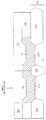
図8は、図4に示すプロセスの後に起こり得る、別のプロセス段階における図1に示す構造100をプログラムされたヒューズ800を表す。図8に示すプログラミングしたヒューズ800は、ポリシリコン層312上に2つのポリシリサイドエリア410A,410Bを有する。この2つのポリシリサイドエリア410A,410Bは、トレース又は電導体804A,804Bに接続される。2つのポリシリサイドエリア410A,410Bは、下位にあるポリシリコン層312の一部を露出する凝集された領域802によって分離されている。
FIG. 8 represents a
図8に示すプログラムされたヒューズ800は、凝集された領域802によって、プリプログラミングの固有抵抗よりレベルの高い、ポストプログラミングの固有抵抗を有する。しかし、若干の電流は、図8において矢印で示されるようにポリシリコン層312を通り抜ける。
The programmed
図9Aは、図5又は図6と図7Aに示すプロセス後に続く、コバルトデポジション、CoSi形成アニール、未反応コバルトの剥離の後に起こり得る図1に示す構造100における別のプロセス段階での、プログラミングされたヒューズ900Aを表す。図5と7Aにおいて、ポリシリコンヒューズ層は、シリサイド化の間、図5と図7Aに示すヒューズエリアのポリシリコン全てが実質的に消滅するように、図4におけるよりも膜厚が比較的薄くなっている(7B参照)。
FIG. 9A illustrates programming at another process stage in the
図9Bは、図5又は図6と図7Aに示すプロセス後に続くコバルトデポジション、CoSi形成アニール、未反応コバルトの剥離の後に起こる、別のプロセス段階で図1の構造100のプログラムされたヒューズ900Bを表す。図9Bにおいて、他のCMOSプロセス条件との関係から、シリサイド化の間(7C参照)に、ポリシリコン許容量910が消耗されることはない。
FIG. 9B illustrates the programmed fuse 900B of the
プログラミング(アグロメレーション)された後、図9Aと図9Bに示すプログラムされたヒューズ900A,900Bは、2つのポリシリサイドエリア902Aと902Bを有する。図9Aに示す2つのポリシリサイドエリア902Aと902Bは、絶縁体106Cの表面につながる、つまり接続状態にある。図9Bに示す2つのポリシリサイドエリア902Aと902Bは、ポリシリコン許容量910とつながる、つまり接続状態にある。
After being programmed (agglomerated), the programmed fuses 900A, 900B shown in FIGS. 9A and 9B have two polysilicide areas 902A and 902B. Two polysilicide areas 902A and 902B shown in FIG. 9A are connected to the surface of the
図9Aと図9Bに示す2つのポリシリサイドエリア902Aと902Bは、プラグ又は電導体906A,906Bに接続される。2つのポリシリサイドエリア902Aと902Bは、図9Aに示す絶縁層の部分106Cと、図9Bに示すポリシリコン910の部分を露出するアグロメレーションした領域904によって分離される。
The two polysilicide areas 902A and 902B shown in FIGS. 9A and 9B are connected to plugs or
図9A,図9Bに示すプログラムされたヒューズ900A,900Bは、アグロメレーションした領域904が図9Aに示す絶縁体106C又は図9Bに示すポリシリコン910の膜厚の薄い層を露出させることから、ポストプログラミング固有抵抗の値は、プリプログラミング固有抵抗の値(高い性能指数)よりも非常に高い(大きなメリットである)、相当高いレベルの値を有する。図9Aの矢線に示されるように、絶縁体106Cを電流が流れることはない。従って、図9Aに示すプログラムされたヒューズ900Aは、理想的なオープン回路(即ち、切断された回路)を形成する。同様に、図9Bに示す絶縁体106Cとポリシリコン層910を通して流れる電流は無視できる程度である。
The programmed fuses 900A, 900B shown in FIGS. 9A and 9B are such that the agglomerated
図10は、コバルトデポジション、コバルトシリコン(CoSi)形成、図5又は図6と図7Aに示すプロセス後の未反応コバルトの剥離の後に起こる、別のプロセス段階におけるプログラムされていなヒューズ1000の上面図である。ヒューズ素子1000のヒューズの長さL、幅W、形状は、低いレベルのボルト数値でプログラムされるように最適化される。コンタクトパッド1002A,1002Bのコンタクトプラグ1004A,1004Bは、ヒューズ1000をプログラミングするための電源供給電圧用にヒューズ素子1000に電気的に接続されるように使用される。
FIG. 10 illustrates the top surface of an
本発明の上述した実施形態は、説明目的のためであって、これに限定されない。種々の変更又は改変が幅広い態様において、本発明の趣旨を離れることなく為される。本発明の精神と目的の範囲内でこうした変更又は改変は、係属中の請求項に包含される。 The above-described embodiments of the present invention are for illustrative purposes and are not limited thereto. Various changes or modifications may be made in a wide range without departing from the spirit of the present invention. Such changes or modifications within the spirit and scope of the invention are encompassed by the pending claims.
Claims (27)
シリコン基板表面を覆うポリシリコン層を形成する過程を有し、前記シリコン基板は前記シリコン基板表面に形成された第1絶縁体を備え、
前記ポリシリコン層を覆うマスク層を形成する過程を有し、前記マスク層は前記第1絶縁体を覆う前記ポリシリコン層の一部領域を露出させるものであり、
概略的なヒューズ構造を形成するために前記ポリシリコン層の前記露出された領域をエッチングする過程を有し、
前記概略的なヒューズ構造を覆うヒューズマスクを形成する過程を有し、前記ヒューズマスクは、前記概略的なヒューズ構造の一部領域を露出させるものであり、
実際のヒューズ構造を形成するために前記概略的なヒューズ構造の前記露出された領域をエッチングする過程を有し、前記概略的なヒューズ構造の前記露出された領域を所定の深さまでエッチし、
前記ポリシリコンの前記露出領域に金属層のデポジットを行う過程を有し、
前記金属層をアニールしてプリプログラムヒューズのポリシリサイド領域を形成する過程を有し、
前記プリプログラムヒューズをプログラミングしてプログラムされたヒューズを形成する過程を有し、前記所定の深さは、前記プログラムされたヒューズがオープン回路を形成するように定められる、方法。A method of forming a polysilicide fuse, comprising:
Forming a polysilicon layer covering the surface of the silicon substrate, the silicon substrate comprising a first insulator formed on the surface of the silicon substrate;
Forming a mask layer covering the polysilicon layer, the mask layer exposing a part of the polysilicon layer covering the first insulator;
Etching the exposed region of the polysilicon layer to form a general fuse structure;
Forming a fuse mask covering the schematic fuse structure, the fuse mask exposing a partial region of the schematic fuse structure;
Etching the exposed region of the schematic fuse structure to form an actual fuse structure, etching the exposed region of the schematic fuse structure to a predetermined depth;
Depositing a metal layer on the exposed region of the polysilicon;
Annealing the metal layer to form a polysilicide region of a preprogrammed fuse ;
Programming the preprogrammed fuse to form a programmed fuse, wherein the predetermined depth is defined such that the programmed fuse forms an open circuit.
約430℃から480℃の温度で約1分間アニールを行ってCoSiを形成する過程と、
未反応Co(コバルト)を剥離する過程と、
約675℃から775℃の温度で数秒間アニールを行うってCoSi2を形成する過程と、を有する、請求項1記載の方法。The annealing process includes
Forming CoSi by annealing at a temperature of about 430 ° C. to 480 ° C. for about 1 minute;
A process of stripping unreacted Co (cobalt);
The method of claim 1 comprising annealing at a temperature of about 675 ° C to 775 ° C for several seconds to form CoSi 2 .
更に、前記ポリシリコン層に裏面反射防止コーティング(BARC;Bottom Anti-Reflective Coating)を形成するとともに前記BARCにフォトレジスト層を形成する過程を有し、
前記フォトレジスト層のトリミングを行って、前記第1絶縁体及び前記第2絶縁体間の前記シリコン基板に第1フォトレジスト層を形成し、前記第1絶縁体上に第2フォトレジスト層を形成する過程を有し、
前記第1及び第2フォトレジスト層を用いて前記BARC及び前記ポリシリコン層部分をエッチングする過程を有し、これによりポリシリコンゲートエリアとポリシリコンヒューズエリアを形成する、請求項1記載の方法。A second insulator on the substrate and separated from the first insulator;
And forming a back antireflection coating (BARC; Bottom Anti-Reflective Coating) on the polysilicon layer and forming a photoresist layer on the BARC;
Trimming the photoresist layer to form a first photoresist layer on the silicon substrate between the first insulator and the second insulator, and forming a second photoresist layer on the first insulator Have the process of
The method of claim 1, comprising etching the BARC and the polysilicon layer portions using the first and second photoresist layers, thereby forming a polysilicon gate area and a polysilicon fuse area.
シリコン基板表面にポリシリコン層を形成する過程を有し、前記シリコン基板は前記シリコン基板の前記表面上の2つのエリアに形成された第1絶縁体と第2絶縁体を備え、
前記ポリシリコン層上に裏面反射防止コーティング(BARC;Bottom Anti-Reflective Coating)を形成する過程を有し、
第1フォトレジスト構造と第2フォトレジスト構造を形成するために前記BARCにフォトレジスト層を形成して、前記フォトレジスト層のトリミングを行う過程を有し、前記第1フォトレジスト構造は、前記BARCの第1エリアと、前記ポリシリコンの第1エリアと、前記第1絶縁体及び前記第2絶縁体間の第1エリアとを覆い、前記第2フォトレジスト構造は、前記BARCの第2エリアと、前記ポリシリコンの第2エリアと、前記第2絶縁体のエリアを覆い、前記第2フォトレジスト構造はヒューズ素子の所定の幅より大きく、
前記BARCを除去し、前記ポリシリコン層部分をエッチングしてポリシリコントランジスタゲート構造と概略的なポリシリコンヒューズ構造を形成する過程を有し、前記概略的なポリシリコンヒューズ構造は前記ヒューズ素子の前記所定の幅より大きいものであり、
前記概略的なヒューズ構造上にヒューズマスクを形成する過程を有し、前記ヒューズマスクは前記概略的なヒューズ構造の一部領域を露出させるものであり、
実際のヒューズ構造を形成するために前記概略的なヒューズ構造の前記露出された領域をエッチングする過程を有し、前記概略的なヒューズ構造の前記露出された領域は所定の深さにエッチングされ、
前記ポリシリコンの前記露出された領域に金属層をデポジットする過程を有し、
前記金属層をアニールしてプリプログラムヒューズのポリシリサイド領域を形成する過程を有し、
前記プリプログラムヒューズをプログラミングしてプログラムされたヒューズを形成する過程を有し、前記所定の深さは、アニールされた後に前記ポリシリサイド領域がオープン回路を形成するように定められ、
ドレイン及びソース領域を形成する過程とを有し、これにより前記トランジスタが形成される、方法。A method for forming an integrated circuit comprising a transistor and a polycide fuse, comprising:
Forming a polysilicon layer on the surface of the silicon substrate, the silicon substrate comprising a first insulator and a second insulator formed in two areas on the surface of the silicon substrate;
Forming a back anti-reflection coating (BARC) on the polysilicon layer;
Forming a photoresist layer on the BARC and trimming the photoresist layer to form a first photoresist structure and a second photoresist structure, wherein the first photoresist structure includes the BARC; A first area of the polysilicon, a first area between the first insulator and the second insulator, and the second photoresist structure includes a second area of the BARC. , Covering the second area of the polysilicon and the area of the second insulator, the second photoresist structure being larger than a predetermined width of the fuse element,
Removing the BARC and etching the polysilicon layer portion to form a polysilicon transistor gate structure and a schematic polysilicon fuse structure, wherein the schematic polysilicon fuse structure includes the step of the fuse element; Is larger than a predetermined width,
Forming a fuse mask on the schematic fuse structure, the fuse mask exposing a partial region of the schematic fuse structure;
Etching the exposed region of the schematic fuse structure to form an actual fuse structure, the exposed region of the schematic fuse structure being etched to a predetermined depth;
Depositing a metal layer on the exposed region of the polysilicon;
Annealing the metal layer to form a polysilicide region of a preprogrammed fuse ;
Programming the preprogrammed fuse to form a programmed fuse, wherein the predetermined depth is defined such that the polysilicide region forms an open circuit after being annealed;
Forming a drain and a source region, whereby the transistor is formed.
シリコン基板を用意する過程を有し、
前記シリコン基板を覆う絶縁体を形成する過程を有し、
前記絶縁体上の前記シリコン基板表面上に直接ポリシリコン層を形成する過程を有し、
前記ポリシリコン層を覆うとともに前記絶縁層上のポリシリコン層の一部領域を露出させるマスク層を形成する過程を有し、
概略的なヒューズ構造を形成するために前記ポリシリコン層の前記露出された 領域をエッチングする過程を有し、
前記概略的なヒューズ構造を覆うとともに前記概略的なヒューズ構造の一部領域を露出させるヒューズマスクを形成する過程を有し、
実際のヒューズ構造を形成するために前記概略的なヒューズ構造の前記露出された領域をエッチングする過程を有し、前記前記概略的なヒューズ構造の前記露出された領域を所定の深さにエッチングされ、
前記ポリシリコン層の前記エッチングされた露出領域に金属層をデポジットする過程を有し、
前記金属層をアニールしてプリプログラムヒューズのポリシリサイド領域を形成する過程を有し、
前記プリプログラムヒューズをプログラミングしてプログラムされたヒューズを形成する過程を有し、前記所定の深さは、前記プログラムされたヒューズがオープン回路を形成するように定められる、方法。A method of forming a polysilicide fuse, comprising:
Having a process of preparing a silicon substrate;
Forming an insulator covering the silicon substrate;
Forming a polysilicon layer directly on the surface of the silicon substrate on the insulator;
Forming a mask layer covering the polysilicon layer and exposing a part of the polysilicon layer on the insulating layer;
Etching the exposed region of the polysilicon layer to form a general fuse structure;
Forming a fuse mask covering the schematic fuse structure and exposing a partial region of the schematic fuse structure;
Etching the exposed region of the schematic fuse structure to form an actual fuse structure, and etching the exposed region of the schematic fuse structure to a predetermined depth. ,
Have a process of depositing a metal layer on the etched exposed regions of the polysilicon layer,
Have a process of forming a poly silicide region of the pre-program fuses by annealing said metal layer,
Programming the preprogrammed fuse to form a programmed fuse, wherein the predetermined depth is defined such that the programmed fuse forms an open circuit.
シリコン基板を形成する過程を有し、
前記シリコン基板を覆う第1絶縁体を形成する過程を有し、
前記第1絶縁体から分離するとともに前記シリコン基板を覆う第2絶縁体を形成する過程を有し、前記第2絶縁体は前記シリコン基板を覆うものであり、
前記シリコン基板表面上にポリシリコン層を形成する過程を有し、前記ポリシリコン層の第1領域は直接前記第1絶縁体上に形成され、前記ポリシリコン層の第2領域は、ゲート領域を形成するために、前記第1絶縁体及び前記第2絶縁体間の前記シリコン基板表面上に形成され、
前記ポリシリコン層を覆うマスク層を形成する過程を有し、前記マスク層は、前記ポリシリコン層の前記第1領域上の第1エリアと、前記ポリシリコン層の第2領域上の第2エリアを露出させる過程を有し、
概略的なヒューズ構造を形成するために前記第1絶縁体上の前記ポリシリコン層の前記露出した第1エリアをエッチングする過程を有し、
前記ヒューズ構造を覆うとともに前記概略的なヒューズ構造の一部領域を露出させる前記ヒューズ構造を形成する過程を有し、
実際のヒューズ構造を形成するために前記概略的なヒューズ構造の前記露出された第1エリアをエッチングする過程を有し、前記概略的なヒューズ構造の前記露出された領域は前記第1絶縁体を超えて所定の深さまでエッチングされるものであり、
前記ポリシリコンの前記エッチングされた露出した第1エリアと前記露出した第2エリアを覆う金属層のデポジットを行う過程を有し、
前記金属層をアニールしてプリプログラムヒューズのポリシリサイド領域を形成する過程を有し、
前記プリプログラムヒューズをプログラミングしてプログラムされたヒューズを形成する過程を有し、前記所定の深さは、前記プログラムされたヒューズがオープン回路を形成するように定められる過程を有し、
前記シリコン基板に前記トランジスタのドレイン及びソースエリアを形成する過程を有する、方法。A method of forming a transistor and a polysilicide fuse,
Having a process of forming a silicon substrate;
Forming a first insulator covering the silicon substrate;
A step of forming a second insulator that separates from the first insulator and covers the silicon substrate, wherein the second insulator covers the silicon substrate;
Forming a polysilicon layer on the surface of the silicon substrate, wherein the first region of the polysilicon layer is formed directly on the first insulator, and the second region of the polysilicon layer includes a gate region; Forming on the silicon substrate surface between the first insulator and the second insulator to form,
Forming a mask layer covering the polysilicon layer, wherein the mask layer includes a first area on the first region of the polysilicon layer and a second area on the second region of the polysilicon layer. The process of exposing
Etching the exposed first area of the polysilicon layer on the first insulator to form a general fuse structure;
Forming the fuse structure covering the fuse structure and exposing a partial region of the schematic fuse structure;
Etching the exposed first area of the schematic fuse structure to form an actual fuse structure, wherein the exposed region of the schematic fuse structure includes the first insulator; It is to be etched to a predetermined depth beyond,
Depositing a metal layer covering the etched exposed first area and the exposed second area of the polysilicon;
Have a process of forming a poly silicide region of the pre-program fuses by annealing said metal layer,
Programming the preprogrammed fuse to form a programmed fuse, and wherein the predetermined depth includes a process in which the programmed fuse is defined to form an open circuit;
Forming a drain and source area of the transistor on the silicon substrate.
シリコン基板を用意する過程を有し、
前記シリコン基板の表面に、前記シリコン基板表面に形成された絶縁体を備えたポリシリコン層を形成する過程を有し、
前記ポリシリコン層を覆うとともに前記絶縁体上のポリシリコン層の一部の領域を露出させるマスク層を形成する過程を有し、
前記ポリシリコン層の前記露出された領域をエッチングして概略的ヒューズ構造を形成する過程を有し、
前記概略的なヒューズ構造上に、前記概略的なヒューズ構造の一部の領域を露出させるヒューズ形成マスクを形成する過程を有し、
前記概略的なヒューズ構造の前記露出された領域をエッチングして実際のヒューズ構造を形成する過程とを有し、前記概略的なヒューズ構造の前記露出された領域は、所定の深さにエッチングされるものであり、
前記ポリシリコンの前記エッチングされた露出された領域上に金属層を形成する過程を有し、
前記金属層をアニールしてプリプログラムヒューズのポリシリサイド領域を形成する過程を有し、
前記プリプログラムヒューズをプログラミングしてプログラムされたヒューズを形成する過程を有し、前記所定の深さは、前記プログラムされたヒューズがオープン回路を形成するように定められる過程を有する、方法。A method for forming an integrated circuit comprising a polysilicide fuse, comprising:
Having a process of preparing a silicon substrate;
Forming a polysilicon layer including an insulator formed on the surface of the silicon substrate on the surface of the silicon substrate;
Forming a mask layer covering the polysilicon layer and exposing a part of the polysilicon layer on the insulator;
Etching the exposed region of the polysilicon layer to form a schematic fuse structure;
Forming a fuse forming mask on the schematic fuse structure to expose a partial region of the schematic fuse structure;
Etching the exposed region of the schematic fuse structure to form an actual fuse structure, wherein the exposed region of the schematic fuse structure is etched to a predetermined depth. And
Forming a metal layer on the etched exposed region of the polysilicon;
Have a process of forming a poly silicide region of the pre-program fuses by annealing said metal layer,
Said programming preprogram fuse has a process of forming a programmed fuse, the predetermined depth, comprising the step of the programmed fuse is determined so as to form an open circuit, method.
Applications Claiming Priority (2)
| Application Number | Priority Date | Filing Date | Title |
|---|---|---|---|
| US10/014,064 US6756255B1 (en) | 2001-12-10 | 2001-12-10 | CMOS process with an integrated, high performance, silicide agglomeration fuse |
| PCT/US2002/039482 WO2003050858A1 (en) | 2001-12-10 | 2002-12-09 | Cmos process with an integrated, high performance, silicide agglomeration fuse |
Publications (3)
| Publication Number | Publication Date |
|---|---|
| JP2005513764A JP2005513764A (en) | 2005-05-12 |
| JP2005513764A5 JP2005513764A5 (en) | 2006-02-02 |
| JP4651941B2 true JP4651941B2 (en) | 2011-03-16 |
Family
ID=21763328
Family Applications (1)
| Application Number | Title | Priority Date | Filing Date |
|---|---|---|---|
| JP2003551823A Expired - Fee Related JP4651941B2 (en) | 2001-12-10 | 2002-12-09 | Method of forming complementary metal oxide semiconductor with integrated high performance silicide agglomerated fuse |
Country Status (9)
| Country | Link |
|---|---|
| US (1) | US6756255B1 (en) |
| EP (1) | EP1451860B1 (en) |
| JP (1) | JP4651941B2 (en) |
| KR (1) | KR100957601B1 (en) |
| CN (1) | CN100352009C (en) |
| AU (1) | AU2002357140A1 (en) |
| DE (1) | DE60224712T2 (en) |
| TW (1) | TWI270961B (en) |
| WO (1) | WO2003050858A1 (en) |
Families Citing this family (12)
| Publication number | Priority date | Publication date | Assignee | Title |
|---|---|---|---|---|
| US20050124097A1 (en) * | 2003-12-05 | 2005-06-09 | Advanced Micro Devices, Inc | Integrated circuit with two phase fuse material and method of using and making same |
| US7645687B2 (en) * | 2005-01-20 | 2010-01-12 | Chartered Semiconductor Manufacturing, Ltd. | Method to fabricate variable work function gates for FUSI devices |
| JP2009506577A (en) * | 2005-08-31 | 2009-02-12 | インターナショナル・ビジネス・マシーンズ・コーポレーション | Random access electrically programmable E-fuse ROM |
| US7417300B2 (en) * | 2006-03-09 | 2008-08-26 | International Business Machines Corporation | Electrically programmable fuse structures with narrowed width regions configured to enhance current crowding and methods of fabrication thereof |
| US7288804B2 (en) * | 2006-03-09 | 2007-10-30 | International Business Machines Corporation | Electrically programmable π-shaped fuse structures and methods of fabrication thereof |
| US7460003B2 (en) * | 2006-03-09 | 2008-12-02 | International Business Machines Corporation | Electronic fuse with conformal fuse element formed over a freestanding dielectric spacer |
| US7784009B2 (en) * | 2006-03-09 | 2010-08-24 | International Business Machines Corporation | Electrically programmable π-shaped fuse structures and design process therefore |
| US7645645B2 (en) * | 2006-03-09 | 2010-01-12 | International Business Machines Corporation | Electrically programmable fuse structures with terminal portions residing at different heights, and methods of fabrication thereof |
| US7924597B2 (en) * | 2007-10-31 | 2011-04-12 | Hewlett-Packard Development Company, L.P. | Data storage in circuit elements with changed resistance |
| US8354304B2 (en) * | 2008-12-05 | 2013-01-15 | Stats Chippac, Ltd. | Semiconductor device and method of forming conductive posts embedded in photosensitive encapsulant |
| CN102549737B (en) * | 2009-08-27 | 2014-09-24 | 松下电器产业株式会社 | Semiconductor device and process for production thereof |
| US8912626B2 (en) | 2011-01-25 | 2014-12-16 | International Business Machines Corporation | eFuse and method of fabrication |
Citations (6)
| Publication number | Priority date | Publication date | Assignee | Title |
|---|---|---|---|---|
| JPS60261154A (en) * | 1984-06-08 | 1985-12-24 | Hitachi Micro Comput Eng Ltd | Semiconductor device |
| JPH0424945A (en) * | 1990-05-16 | 1992-01-28 | Seiko Instr Inc | Manufacture of semiconductor device |
| JPH10199712A (en) * | 1996-12-27 | 1998-07-31 | Vlsi Technol Inc | Two-layer type programmable resistor |
| JPH10340663A (en) * | 1997-03-07 | 1998-12-22 | St Microelectron Sa | Pseudo-fuse and circuit using pseudo-fuse |
| JP2001077050A (en) * | 1999-08-31 | 2001-03-23 | Toshiba Corp | Manufacture of semiconductor device |
| JP2001326242A (en) * | 2000-05-16 | 2001-11-22 | Matsushita Electric Ind Co Ltd | Semiconductor device and method of fabrication |
Family Cites Families (9)
| Publication number | Priority date | Publication date | Assignee | Title |
|---|---|---|---|---|
| US4042950A (en) * | 1976-03-01 | 1977-08-16 | Advanced Micro Devices, Inc. | Platinum silicide fuse links for integrated circuit devices |
| US4647340A (en) * | 1986-03-31 | 1987-03-03 | Ncr Corporation | Programmable read only memory using a tungsten fuse |
| US6337507B1 (en) * | 1995-09-29 | 2002-01-08 | Intel Corporation | Silicide agglomeration fuse device with notches to enhance programmability |
| US5708291A (en) * | 1995-09-29 | 1998-01-13 | Intel Corporation | Silicide agglomeration fuse device |
| US5821160A (en) * | 1996-06-06 | 1998-10-13 | Motorola, Inc. | Method for forming a laser alterable fuse area of a memory cell using an etch stop layer |
| US6022775A (en) | 1998-08-17 | 2000-02-08 | Taiwan Semiconductor Manufacturing Company | High effective area capacitor for high density DRAM circuits using silicide agglomeration |
| US6242790B1 (en) | 1999-08-30 | 2001-06-05 | Advanced Micro Devices, Inc. | Using polysilicon fuse for IC programming |
| US6391767B1 (en) * | 2000-02-11 | 2002-05-21 | Advanced Micro Devices, Inc. | Dual silicide process to reduce gate resistance |
| US6642601B2 (en) * | 2000-12-18 | 2003-11-04 | Texas Instruments Incorporated | Low current substantially silicide fuse for integrated circuits |
-
2001
- 2001-12-10 US US10/014,064 patent/US6756255B1/en not_active Expired - Lifetime
-
2002
- 2002-12-09 KR KR1020047008979A patent/KR100957601B1/en not_active IP Right Cessation
- 2002-12-09 CN CNB02824656XA patent/CN100352009C/en not_active Expired - Fee Related
- 2002-12-09 DE DE60224712T patent/DE60224712T2/en not_active Expired - Lifetime
- 2002-12-09 JP JP2003551823A patent/JP4651941B2/en not_active Expired - Fee Related
- 2002-12-09 WO PCT/US2002/039482 patent/WO2003050858A1/en active IP Right Grant
- 2002-12-09 AU AU2002357140A patent/AU2002357140A1/en not_active Abandoned
- 2002-12-09 EP EP02804766A patent/EP1451860B1/en not_active Expired - Lifetime
- 2002-12-10 TW TW091135639A patent/TWI270961B/en not_active IP Right Cessation
Patent Citations (6)
| Publication number | Priority date | Publication date | Assignee | Title |
|---|---|---|---|---|
| JPS60261154A (en) * | 1984-06-08 | 1985-12-24 | Hitachi Micro Comput Eng Ltd | Semiconductor device |
| JPH0424945A (en) * | 1990-05-16 | 1992-01-28 | Seiko Instr Inc | Manufacture of semiconductor device |
| JPH10199712A (en) * | 1996-12-27 | 1998-07-31 | Vlsi Technol Inc | Two-layer type programmable resistor |
| JPH10340663A (en) * | 1997-03-07 | 1998-12-22 | St Microelectron Sa | Pseudo-fuse and circuit using pseudo-fuse |
| JP2001077050A (en) * | 1999-08-31 | 2001-03-23 | Toshiba Corp | Manufacture of semiconductor device |
| JP2001326242A (en) * | 2000-05-16 | 2001-11-22 | Matsushita Electric Ind Co Ltd | Semiconductor device and method of fabrication |
Also Published As
| Publication number | Publication date |
|---|---|
| KR100957601B1 (en) | 2010-05-13 |
| EP1451860A1 (en) | 2004-09-01 |
| JP2005513764A (en) | 2005-05-12 |
| KR20040064302A (en) | 2004-07-16 |
| DE60224712T2 (en) | 2009-01-29 |
| TW200301549A (en) | 2003-07-01 |
| DE60224712D1 (en) | 2008-03-06 |
| CN1695232A (en) | 2005-11-09 |
| TWI270961B (en) | 2007-01-11 |
| EP1451860B1 (en) | 2008-01-16 |
| AU2002357140A1 (en) | 2003-06-23 |
| WO2003050858A1 (en) | 2003-06-19 |
| CN100352009C (en) | 2007-11-28 |
| US6756255B1 (en) | 2004-06-29 |
Similar Documents
| Publication | Publication Date | Title |
|---|---|---|
| US9275956B2 (en) | Semiconductor integrated circuit device and process for manufacturing the same | |
| US6071784A (en) | Annealing of silicon oxynitride and silicon nitride films to eliminate high temperature charge loss | |
| JPH05136269A (en) | Programmable interconnection device and manufacture thereof | |
| JP4651941B2 (en) | Method of forming complementary metal oxide semiconductor with integrated high performance silicide agglomerated fuse | |
| KR100698501B1 (en) | Bottom anti-reflective coating using rapid thermal anneal with oxidizing gas | |
| US7919367B2 (en) | Method to increase charge retention of non-volatile memory manufactured in a single-gate logic process | |
| US6080661A (en) | Methods for fabricating gate and diffusion contacts in self-aligned contact processes | |
| US6436759B1 (en) | Method for fabricating a MOS transistor of an embedded memory | |
| US6939810B2 (en) | Method of forming isolation film | |
| US6365509B1 (en) | Semiconductor manufacturing method using a dielectric photomask | |
| JP2668490B2 (en) | Mask ROM manufacturing method | |
| US20210384202A1 (en) | Semiconductor structure and method of forming the same | |
| US20230402115A1 (en) | Method of manufacturing semiconductor device with programmable feature | |
| US20230402114A1 (en) | Semiconductor device with programmable feature | |
| KR940000516B1 (en) | Method of fabricating a mask rom | |
| JP2003526941A (en) | One-time programmable anti-fuse element and method of manufacturing the same |
Legal Events
| Date | Code | Title | Description |
|---|---|---|---|
| A521 | Written amendment |
Free format text: JAPANESE INTERMEDIATE CODE: A523 Effective date: 20051209 |
|
| A621 | Written request for application examination |
Free format text: JAPANESE INTERMEDIATE CODE: A621 Effective date: 20051209 |
|
| A977 | Report on retrieval |
Free format text: JAPANESE INTERMEDIATE CODE: A971007 Effective date: 20080116 |
|
| A131 | Notification of reasons for refusal |
Free format text: JAPANESE INTERMEDIATE CODE: A131 Effective date: 20091006 |
|
| A601 | Written request for extension of time |
Free format text: JAPANESE INTERMEDIATE CODE: A601 Effective date: 20100106 |
|
| A602 | Written permission of extension of time |
Free format text: JAPANESE INTERMEDIATE CODE: A602 Effective date: 20100114 |
|
| A601 | Written request for extension of time |
Free format text: JAPANESE INTERMEDIATE CODE: A601 Effective date: 20100208 |
|
| A602 | Written permission of extension of time |
Free format text: JAPANESE INTERMEDIATE CODE: A602 Effective date: 20100216 |
|
| A601 | Written request for extension of time |
Free format text: JAPANESE INTERMEDIATE CODE: A601 Effective date: 20100308 |
|
| A602 | Written permission of extension of time |
Free format text: JAPANESE INTERMEDIATE CODE: A602 Effective date: 20100315 |
|
| A521 | Written amendment |
Free format text: JAPANESE INTERMEDIATE CODE: A523 Effective date: 20100330 |
|
| RD03 | Notification of appointment of power of attorney |
Free format text: JAPANESE INTERMEDIATE CODE: A7423 Effective date: 20100421 |
|
| A131 | Notification of reasons for refusal |
Free format text: JAPANESE INTERMEDIATE CODE: A131 Effective date: 20100519 |
|
| A601 | Written request for extension of time |
Free format text: JAPANESE INTERMEDIATE CODE: A601 Effective date: 20100810 |
|
| A602 | Written permission of extension of time |
Free format text: JAPANESE INTERMEDIATE CODE: A602 Effective date: 20100817 |
|
| A601 | Written request for extension of time |
Free format text: JAPANESE INTERMEDIATE CODE: A601 Effective date: 20100901 |
|
| RD05 | Notification of revocation of power of attorney |
Free format text: JAPANESE INTERMEDIATE CODE: A7425 Effective date: 20100902 |
|
| A602 | Written permission of extension of time |
Free format text: JAPANESE INTERMEDIATE CODE: A602 Effective date: 20100908 |
|
| A521 | Written amendment |
Free format text: JAPANESE INTERMEDIATE CODE: A523 Effective date: 20101019 |
|
| TRDD | Decision of grant or rejection written | ||
| A01 | Written decision to grant a patent or to grant a registration (utility model) |
Free format text: JAPANESE INTERMEDIATE CODE: A01 Effective date: 20101117 |
|
| A01 | Written decision to grant a patent or to grant a registration (utility model) |
Free format text: JAPANESE INTERMEDIATE CODE: A01 |
|
| A61 | First payment of annual fees (during grant procedure) |
Free format text: JAPANESE INTERMEDIATE CODE: A61 Effective date: 20101215 |
|
| R150 | Certificate of patent or registration of utility model |
Free format text: JAPANESE INTERMEDIATE CODE: R150 |
|
| FPAY | Renewal fee payment (event date is renewal date of database) |
Free format text: PAYMENT UNTIL: 20131224 Year of fee payment: 3 |
|
| LAPS | Cancellation because of no payment of annual fees |