JP4643003B2 - Cooling device for optical crystal or laser crystal, respectively - Google Patents
Cooling device for optical crystal or laser crystal, respectively Download PDFInfo
- Publication number
- JP4643003B2 JP4643003B2 JP2000522654A JP2000522654A JP4643003B2 JP 4643003 B2 JP4643003 B2 JP 4643003B2 JP 2000522654 A JP2000522654 A JP 2000522654A JP 2000522654 A JP2000522654 A JP 2000522654A JP 4643003 B2 JP4643003 B2 JP 4643003B2
- Authority
- JP
- Japan
- Prior art keywords
- laser crystal
- cooling
- laser
- crystal
- crystal device
- Prior art date
- Legal status (The legal status is an assumption and is not a legal conclusion. Google has not performed a legal analysis and makes no representation as to the accuracy of the status listed.)
- Expired - Fee Related
Links
Images


Classifications
-
- H—ELECTRICITY
- H01—ELECTRIC ELEMENTS
- H01S—DEVICES USING THE PROCESS OF LIGHT AMPLIFICATION BY STIMULATED EMISSION OF RADIATION [LASER] TO AMPLIFY OR GENERATE LIGHT; DEVICES USING STIMULATED EMISSION OF ELECTROMAGNETIC RADIATION IN WAVE RANGES OTHER THAN OPTICAL
- H01S3/00—Lasers, i.e. devices using stimulated emission of electromagnetic radiation in the infrared, visible or ultraviolet wave range
- H01S3/02—Constructional details
- H01S3/025—Constructional details of solid state lasers, e.g. housings or mountings
-
- H—ELECTRICITY
- H01—ELECTRIC ELEMENTS
- H01S—DEVICES USING THE PROCESS OF LIGHT AMPLIFICATION BY STIMULATED EMISSION OF RADIATION [LASER] TO AMPLIFY OR GENERATE LIGHT; DEVICES USING STIMULATED EMISSION OF ELECTROMAGNETIC RADIATION IN WAVE RANGES OTHER THAN OPTICAL
- H01S3/00—Lasers, i.e. devices using stimulated emission of electromagnetic radiation in the infrared, visible or ultraviolet wave range
- H01S3/02—Constructional details
- H01S3/04—Arrangements for thermal management
- H01S3/042—Arrangements for thermal management for solid state lasers
-
- H—ELECTRICITY
- H01—ELECTRIC ELEMENTS
- H01S—DEVICES USING THE PROCESS OF LIGHT AMPLIFICATION BY STIMULATED EMISSION OF RADIATION [LASER] TO AMPLIFY OR GENERATE LIGHT; DEVICES USING STIMULATED EMISSION OF ELECTROMAGNETIC RADIATION IN WAVE RANGES OTHER THAN OPTICAL
- H01S3/00—Lasers, i.e. devices using stimulated emission of electromagnetic radiation in the infrared, visible or ultraviolet wave range
- H01S3/02—Constructional details
- H01S3/025—Constructional details of solid state lasers, e.g. housings or mountings
- H01S3/027—Constructional details of solid state lasers, e.g. housings or mountings comprising a special atmosphere inside the housing
-
- H—ELECTRICITY
- H01—ELECTRIC ELEMENTS
- H01S—DEVICES USING THE PROCESS OF LIGHT AMPLIFICATION BY STIMULATED EMISSION OF RADIATION [LASER] TO AMPLIFY OR GENERATE LIGHT; DEVICES USING STIMULATED EMISSION OF ELECTROMAGNETIC RADIATION IN WAVE RANGES OTHER THAN OPTICAL
- H01S3/00—Lasers, i.e. devices using stimulated emission of electromagnetic radiation in the infrared, visible or ultraviolet wave range
- H01S3/02—Constructional details
- H01S3/04—Arrangements for thermal management
- H01S3/0405—Conductive cooling, e.g. by heat sinks or thermo-electric elements
-
- H—ELECTRICITY
- H01—ELECTRIC ELEMENTS
- H01S—DEVICES USING THE PROCESS OF LIGHT AMPLIFICATION BY STIMULATED EMISSION OF RADIATION [LASER] TO AMPLIFY OR GENERATE LIGHT; DEVICES USING STIMULATED EMISSION OF ELECTROMAGNETIC RADIATION IN WAVE RANGES OTHER THAN OPTICAL
- H01S3/00—Lasers, i.e. devices using stimulated emission of electromagnetic radiation in the infrared, visible or ultraviolet wave range
- H01S3/09—Processes or apparatus for excitation, e.g. pumping
- H01S3/091—Processes or apparatus for excitation, e.g. pumping using optical pumping
- H01S3/094—Processes or apparatus for excitation, e.g. pumping using optical pumping by coherent light
- H01S3/094038—End pumping
-
- H—ELECTRICITY
- H01—ELECTRIC ELEMENTS
- H01S—DEVICES USING THE PROCESS OF LIGHT AMPLIFICATION BY STIMULATED EMISSION OF RADIATION [LASER] TO AMPLIFY OR GENERATE LIGHT; DEVICES USING STIMULATED EMISSION OF ELECTROMAGNETIC RADIATION IN WAVE RANGES OTHER THAN OPTICAL
- H01S3/00—Lasers, i.e. devices using stimulated emission of electromagnetic radiation in the infrared, visible or ultraviolet wave range
- H01S3/23—Arrangements of two or more lasers not provided for in groups H01S3/02 - H01S3/22, e.g. tandem arrangements of separate active media
- H01S3/2308—Amplifier arrangements, e.g. MOPA
- H01S3/2325—Multi-pass amplifiers, e.g. regenerative amplifiers
Landscapes
- Physics & Mathematics (AREA)
- Electromagnetism (AREA)
- Engineering & Computer Science (AREA)
- Plasma & Fusion (AREA)
- Optics & Photonics (AREA)
- Lasers (AREA)
Description
【0001】
本発明は熱的に高い負荷がかかる、レーザビーム、特に、レーザパルスが得られる光学クリスタル、または、レーザクリスタル、それぞれ、のための、例えば、光学増幅器または発振器のレーザクリスタルのためのペルチエ要素を具備する冷却装置に関する。
【0002】
レーザ装置内の光学クリスタル、または、レーザクリスタル、それぞれ、以下、単に”クリスタル”と言う、の冷却は、クリスタル、例えば、チタン−サファイアクリスタル(一般的には、Ti:S laser crystalと言われる)が、運転中に高い熱負荷にさらされる場合には特に重要である。これは、例えば、受動的にモードロックされた(mode-locked) 短パルスのレーザ装置(発振器)内でクリスタルが光学的に非直線的な要素(non-linear element)として使用され、ポンプビームとレゾネータビームがクリスタル内で出来るかぎり高度に焦点合わせされる場合であって、その様にする際、クリスタルは、小さな寸法でなければならず、また、それを補償するために、材料の分散を低く保持するべく高く寄与しなければならず、そのため、未公開の先の出願WO−98/10 494−Aに述べられているように、特定の、熱的な負荷が上昇する。また、10°C以下への冷却は、その時に起こる湿気の凝縮、その際クリスタルの上で凝縮した小さな滴がクリスタルを急激に損傷し、あるいは、破壊する、ので問題であるということも述べられている。
【0003】
特に重要なのは、さらに、光学増幅器の場合のクリスタルの冷却であって、すでに、1997年8月15日発行のOptics Lertters の Vol.22,No.16の1256頁〜1258頁のバックス他(Backus et al)による論文、”0.2−TW laser system at 1 kHz”に述べられている通りである。この様な、発振器の光学的な後増幅(post-amplification) においては、例えば、やはりチタン−サファイアレーザクリスタルが使用され、そこでは、発振器からの数nJのエネルギを有するパルスは1mJのオーダーに増幅される(すなわち、106 の率だけ)。この目的のために、チタン−サファイア増幅クリスタルが緑のレーザ光、で”ポンプ”され、それは、例えば、10〜20Wの平均出力を有し、それは発振器内でのレーザパルス発生でのポンピング出力の倍数である。
【0004】
光学的増幅器はパルス(パルス周波数は略1kHzである)により作動されるという事実から、ポンピングエネルギは独立のパルスに集中され、それが発振器のパルスを増幅する。そこで発生する高い出力により、クリスタルの充分な冷却が重要である。クリスタル冷却が不十分だと、効率が低いだけでなく、発振器に関するのと同様に、”熱レンズ(thermal lense)”効果による”好ましくないビーム形状を誘起し、それも、前述のバックス他による論文に述べられている。
【0005】
クリスタルが熱せられると、それにより発生する材料内部の温度勾配は屈折率勾配を誘起し、それは、クリスタル材料によっては、レーザビームが通過する間に意図しない焦点合わせ、あるいは、非焦点化をおこなう。クリスタルの良好な冷却は低い温度で熱伝導率を向上し、屈折率の温度係数を小さくし、略理想的なガウス強度形状(Gaussian intensity profile) (断面において)に対応したビームの形状を得ることができる。さらに効率の度合いが向上する。
【0006】
バックス他による論文によれば液体窒素がクリスタルの冷却に使用され、それにより極めて低温を得ることを可能にしている、しかし、それにより、多くの目的のための、特に移動する使用のための、実際的な光学的増幅器の具現化が阻害されている。
【0007】
若干異なる光学的増幅器が、1997年10月15日発行のOptics Lertters の Vol.22,No.20のサルタニア他(Sartania et al)による論文、”0.2−TW 5−fs optical pulse at a 1−kHz”に述べられており、そこでは、ペルチエ冷却装置がクリスタルの冷却に使用されていることが概論されている。しかし、協力な冷却によって、クリスタルの上で凝縮された水のみならず、氷が形成され、空気中に汚れがあり、それがクリスタル上に堆積するという問題は残っている。実際、このような氷の形成、汚れは、クリスタル表面の腐食による、局所的な破壊につながる。
【0008】
本発明の目的は、上述の欠点を克服し、一方で、簡単な構成にも係わらず特に移動する適用形態にも好適ならしめ、高い効率の良好な冷却と最適なビーム形状を得ることができ、他方で、凝縮された水(氷)、や不純物による腐食を防止することによってレーザクリスタルの長い寿命を確保できる、最初に規定したタイプの冷却装置を提供することである。
【0009】
本発明は、光学用のレーザクリスタル装置を提供する。レーザクリスタル装置は、レーザクリスタル(5)と、該レーザクリスタルのためのペルチエ要素(18)を含む冷却装置(7)とを具備する。レーザクリスタルは、稼動において、10ワット以上の光学的動力の熱的に高い負荷がかけられており、レーザクリスタルからレーザパルス(2)が生得されており、レーザクリスタル(5)が熱伝導性の良い材料から成る冷却ジョー(24、25)の間に支持されており、レーザクリスタル(5)は、レーザクリスタルを冷却するために備えられるペルチエ要素(18)及び冷却ジョー(24、25)と共に、密封容器(8)に収容されており、密封容器(8)は、その内部が真空排気されており、更に密封容器(8)が、ブリュースター角に対応する光学軸に対して角度を成して配設されたレーザパルス(2)の通過のための少なくとも1つのブリュースター窓(32、33)を有することを特徴とする。
【0010】
密封容器を提供することにより、容器の内部を真空排気すること、または、乾燥状態に保つことが可能になり、凝縮された水が、光学クリスタル、または、レーザクリスタル、それぞれ、の上に堆積しない、さらには、クリスタルに対して画成されたクリーンな環境(真空、または、純粋な、すなわち、汚れのない、乾燥した空気)が可能になる。このようにして長い運転時間を得ることができ、それは光学クリスタル、または、レーザクリスタルの装着の間の、あるいは、精密な調整の間に必要な消費という点でも大きな利点である。
【0011】
さらには、本発明の冷却装置は、熱弾性的な冷却要素、すなわち、ペルチエ要素、を密封容器と共に使用することにより、コンパクトで、簡単で、扱いやすいレーザ装置の構造が可能となって、それによって、さらに、何ら問題なく車両内での使用、例えば、また航空機内での使用を可能にしたことを特徴とするが、それは、液体窒素による冷却に比して、運転中、重力の影響を受けないことによる。容器は、強く閉めることのできる真空排気のための連結手段、および、ペルチエ要素へ電力を供給するための強く密封できる電線の通路を備えることができる。
【0012】
当該適用において発生する高い強度の点から、いわゆるレーザビームの通過のためのブリュースター窓が容器に設けれている。この様にして、すなわち、そうでなければ使用される広い幅の屈折防止コーティングをすることなく、意図しない屈折を防止することができる。というのは、この様な、誘電コーティング(dielectric coating)は前述の高い強度に耐えることができない(例えば、ビーム径が10mm以下で、ピーク出力がMWからGWの範囲でパルス持続時間が10fsからpsの範囲で、平均出力が10mWから始まってWまでの範囲であり、ポンプパラメータについては、平均出力が数Wから数十W、ポンプエネルギが数mJ、高反復周波数がkHzの範囲で、これがピーク出力をMWからGWの範囲に導く)。
【0013】
半導体レーザについては密封モジュールを使用することが知られており、例えば、ドイツ特許DE3307933C、ドイツ特許DE3922800A、日本特許公開JP1−122183A、あるいは、欧州特許EP259888Aを参照、そこでは、ペルチエ要素をともなったレーザダイオード要素が示されている。しかしながら、高いレーザ出力はなく、レーザダイオード要素には低い熱負荷しかかからず、ペルチエ要素は実際は単に温度を安定化させる目的でしか使用されない。公知の半導体レーザではこれは重要である、というのは、レーザダイオードの場合、レーザ波長は基本的に半導体チップの温度に依存し、多くの場合、正しい波長を得るために加熱さえ必要とされる。
さらに、これらの公知の装置においては、乾燥材によるモジュールの真空排気、または、乾燥には言及していない。
【0014】
ペルチエ要素によって、多くの場合、何ら問題なくレーザクリスタルの充分な冷却をおこなうことができる、また多くの場合ペルチエ要素における50〜70°Cの温度差で充分であることが示されている。特に顕著な、レーザクリスタルからの熱発散、あるいは、冷却のためには、ペルチエ要素を積み重ねて設けることが有利である。この場合には、熱側が大気温度(約20°C)の際に、冷側で−50〜−100°Cを得ることは容易である。この様に、従来のペルチエ要素を使用した場合、130°Cにも達するペルチエ要素の温度差を得ることができ、−100°C以下での冷却をおこなうことができる。
【0015】
光学クリスタル、または、レーザクリスタル、それぞれは、小板形状にされ、また、良好な冷却を得るために、比較的小さな諸元を有し、増幅器と共に使用する場合は、幅、長さが約3mm、高さ1〜1.5mmに過ぎない。
【0016】
良好な熱の転移、及び、熱発散を確保しつつ、クリスタルを固定するためには、クリスタルを、ペルチエ要素が置かれる良好な熱伝導性の冷却ジョーの間に配置することが有利である。その際に、出来るだけ大きな熱の転移面、並びに、特に簡単なクリスタルの保持を得るためには、冷却ジョーが実際的にクリスタルを四つの側から抱くようにすることが好ましい。
【0017】
製造および装着の点で好ましい解決は、さらに、クリスタルにその対向する側で載っている2つの冷却ジョーの内の1つが、他方の冷却ジョーの上に載っているクリスタルの上まで延伸するノーズ突起を有し、冷却ジョーがクリスタルの前と後に、レーザビームの方向に、レーザビームを通すための凹部を備えるようにすることである。
【0018】
ペルチエ要素の”熱”側を大気温度(あるいはもっと低く)に保つことは、ペルチエ要素が冷却ジョーから離れる向きの熱側で冷却受け台と係合している場合にはさらに有利である。ペルチエ要素の熱側を効率よく冷却するためには冷却受け台を液体冷却することが有利であることが明らかにされている。冷却受け台は、全くどの様な、例えば、立方形や円板形のような形状、でもよい。高い冷却貯蔵容量を得るため、並びに、ペルチエ要素と冷却ジョーの安定した調和のため、簡単に製造するため、に、冷却受け台を、端部にペルチエ要素並びに冷却ジョーをクリスタルに調和させる略V字形状の凹部を有する略円筒状に形成することがさらに好ましい。
【0019】
工程上の理由から、また、ペルチエ要素の受け面のために、V字形状の凹部が90°の頂角を有することが有利である。ペルチエ要素を方向付けするために、また、その装着を容易にするために、さらに、V字形状の凹部が傾斜したペルチエ要素の載置面を画成し、ペルチエ要素のための載置面から上方に突出する停止具を内側の、載置面に隣接した端部に設けることが有利である。
【0020】
容器が蓋で閉じられる円筒状のケーシングを備える場合には、例えば、Oリングによって、良好なシールを得ることのできる特に簡単なデザインの密封タイプの容器を得ることができる。これに関して、冷却受け台がペルチエ要素から離れる向きの端部側に管状のケーシングを強く結合できるフランジを備えることがさらに有利である。冷却受け台がフランジの領域に冷却液を通す穴を備えることも有利である。
【0021】
レーザビームが、窓を通過する際に、(短い運転時間で窓の腐食、破壊を起こさないように)単位面積当たり比較的低い出力を有するようにするために、レーザビームは窓の位置、においてできるだけ広い断面を有する、すなわち、焦点が合っていない、ことが必要であり、これは窓はクリスタルからある距離(例えば、約8〜10cm)を隔てていなければならないということを意味する。これを容器全体を大きくしないで可能とするために、密封容器が、好ましくは、その対向する側に、突出した、強く取り付けられた、その外側端部がレーザビームを通すための窓で閉じられたパイプソケットを備えることが好ましい。
本発明は、上述の冷却装置を備えたレーザ装置にも関わる。
【0022】
以下、本発明の詳細を図面に示された例示的実施の形態によって説明するが、それに限定されるものではない。
以下において、本発明による冷却装置が図1に基本的部品で概略図示されるように例を用いて光学増幅器と共により詳細に説明される。冷却装置は効率的な冷却効果により光学増幅器において特に利点を有するが、他のレーザ装置、例えば、発振器付きのものにも使用できる。さらには、光学クリスタル、または、レーザクリスタル、それぞれ、のために以下で示される材料は、それぞれ(チタン−サファイアクリスタル)、ポンプレーザ(周波数が2重にされた、Nd−YLFレーザ、ニオディム−イットリウム−リチウム−フッ素レーザ)の構造のために示されたものと共に、単なる例に過ぎない。
【0023】
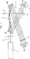
図1には、光学増幅器の基本的な構成要素の装置が概略図示されていて、そこでは、図示の例において、光学増幅器がいわゆる”マルチパス増幅器”、として示されている。前述のバックス他による論文、”0.2−TW laser system at 1 kHz”参照。本発明は、勿論、他の光学増幅器、すなわち、特に、例えば、ポッケルズ セル(Pockels cells)によってレーザビームが増幅器を出る前に繰り返される、レーザビームの共直線的(colinear)な通路が発生するいわゆる再生増幅器、にも適用できる。
【0024】
詳細には、図1に、ポンプレーザ、例えば、周波数が2重にされた、Nd−YLFレーザ、が1で概略的に示されていて、それは図1において2で示されるレーザパルスのためのエネルギを供給するレーザビーム、いわゆるポンプビーム、を出力する。3で、これらのレーザパルスは詳しく示されていない図示されない従来のレーザ発振器によって、全体が4で示される増幅器装置そのものに供給される。この増幅器装置4のための基本的な要素は、以下、単にクリスタルという、例えば、Ti:Sクリスタルのような、光学クリスタル、または、レーザクリスタル5であって、図1においては冷却装置もなく極めて概略的に示されており、このクリスタル内では、レーザビームは対応する矢印によって示される色々な通路によって焦点合わせがされる。特に、クリスタル5の両側に、ビームを増幅するための、焦点合わせ用のミラーM1、M2が設けられていて、少なくとも、焦点合わせ用のミラーM1は半透明にされ焦点合わせ用レンズL1から来たポンプビーム2がクリスタル5を通過できるようにしている。
【0025】
さらには、図1にはビームを増幅するための後部リフレクタ(retroreflector)がR1、R2で示されていて、それは空間内にレーザビームの色々なマルチパス位置(multipass-positions)を提供し、後部リフレクタR1は、さらに、互いに予め定めた間隔で配列され、発振器から到着したレーザパルスはそこでしかるべく形成されたギャップを通って増幅器装置4内に進入する。それから、4、6、あるいは8個の穴から成る開口Aが後部リフレクタR1の前に配設され増幅器4内のレーザの活動を抑制し、ミラー6が強化されたレーザパルスを減結合(decoupling) するために設けられている。強化されたレーザパルスPは、それ自体公知であるので詳細が図示されていない圧縮器に供給され、この圧縮器内においてレーザパルスはその持続時間に関して短縮される。
【0026】
光学的な増幅のために、ポンプレーザ1が使用され、それは、例えば、周波数が約1kHzで平均出力が10〜20Wのパルスを発生する。増幅すべきレーザパルスは発振器から何倍か高い周波数で到着するので、通常は、増幅されていないパルスを抑制するために、例えば、ポッケルズセルを備える装置が増幅装置と組み合わせて使用される、しかし、それは、図1には示されていない。
【0027】
この点に関するさらなる情報としては、既に述べた、サルタニア他の”Generation of 0.1−TW 5−fs optical pulse at a 1−kHz repetetion rate”、あるいは、バックス他の”0.2−TW laser system at 1 kHz”を参照することができる。より良く理解するためには、例えば、発振器から到着するレーザパルスは75 MHzの周波数を有し、各75000毎のパルスしか通過してポンプレーザからのエネルギで増強されない、ということに留意すべきである。
【0028】
ポンプパルスが有する高出力の点、並びに、比較的小さいクリスタル体積におけるポンプパルスの焦点合わせの点から、対応してそこでは高い熱量が発生し、クリスタルの効率的な冷却が非常に重要となる。さらに、増幅器、または、一般的には、レーザ装置の産業的な適用の点から、公知の装置のような液体窒素による冷却は、好適ではなく、扱い難く、さらには、重力の影響を受けるので、移動性の使用に適していない。
【0029】
以下、全体が7で示される冷却装置を図2〜9によって説明する、この冷却装置は、充分な冷却、コンパクト、シンプル、扱いやすい構造、重力に左右されない、等の各要求を充たし、さらには、クリスタルを長期に使用することができるということを特徴としている。
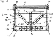
【0030】
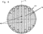
図2、3から明らかなように、冷却装置7は封入容器タイプの、強く閉じられる容器8を具備し、それは端部側フランジ10、11を有する管状ケーシング9を有し、端部側フランジ10、11には蓋12と冷却受け台13がねじ14、と、一方はフランジ10、11、他方は蓋12、または、冷却受け台13の間に設けられた補助的なゴム、または弾性プラスチックから成るOリングシール15、によってフランジ13aを介して固定されている。
【0031】
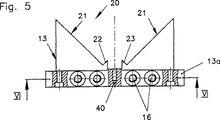
図5、6から特に明らかなように、冷却受け台13は冷却液、例えば水、を通すための4つの平行な穴16、穴16の端部にねじこまれた連結部材17(図2参照)を備え、それは図2において破線で示されるダクト、または、ホースによる穴16の連続的な切替えの役を成す。冷却液は矢印Eにそって入り、矢印Aにそって出ていく。
冷却受け台13は、例えば、銅、または、アルミニウムでつくられるが、蓋12は、例えば、プラスチックから成り、管状ケーシング9は、例えば、アルミニウムから成る。
【0032】
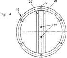
冷却受け台13の底部から、外側が略円筒状のボディ19が上方に延伸し、それはペルチエ要素18を載置せしめ、管状ケーシング9の内壁に接している、例えば、ペルチエ要素18は商業的にはMelcor Thermoelectronics 2 2 SC 055 045−123−63の名称で入手可能である。この中間部分においては、ボディ19は、90°の頂角を備えて、センタラインL(図2参照)の両側にペルチエ要素の2つの載置面21を画成するのV字形の凹部20を有し、載置面21の内側の隣接する端部は上方に突出するペルチエ要素のための停止具22、23を有する。
【0033】
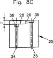
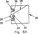
図示の例示的な実施の形態においては、ペルチエ要素の2つのブロックがそれぞれ両載置面21の上に重ね合わせに積み重ねられている。ペルチエ要素の熱放射側、または、”熱”側は両載置面21に接し、熱吸収側、または、”冷”側は、ペルチエ要素を所定位置に固定し、詳細が図7A〜7C、図8A〜8Cに示される形状を有する冷却ジョー24、25に接している。
【0034】
図7B、図8Bの正面図に特に明らかなように、冷却ジョー24、25は横の角度が、例えば、45°の略楔状にされ、装着状態において、ボディ19の頂角90°の凹部を埋める。図2の中心線Lの右側に配設されている冷却ジョー25はノーズ突起26(図8B参照)を有し、それは、図2の中心線Lの左側に配設された冷却ジョー24を超えて延伸し、下側でクリスタル5に接していて(図2、3に加え、図9も参照)、クリスタル5は冷却ジョー24の段差状の凹部27内にある(図7B参照)。クリスタル5は中心線Lに平行な光主軸を有する平行管の形状を有し、例えば、主軸に対し約60°の角度を有する端面を有する。
【0035】
図8Aの冷却ジョー25の上面図から明らかなのは、クリスタル5の上にあるノーズ突起26も60°の角度で延伸していて、図8A内のノーズ突起26の上縁に続いて、冷却ジョー25も中心線Lに対して60°の角度でやはり延伸する境界線を有する段差状の凹部28を有していることである。
【0036】
同様にして、またノーズ突起の想像延長において、冷却ジョー24は段差状の凹部29を有し、図2、図7A参照、それは同様に中心線Lに対して60°の角度で斜めに延伸している。
【0037】
冷却ジョー25の段差部分28の深さと冷却ジョー24の段差部分29の深さT1 は等しく、冷却ジョー24の段差部分27の深さT2 よりも大きい。ノーズ突起26の高さHは段差部分27の深さT2 に対応し、クリスタル5の厚さだけ小さい。
【0038】
このように、冷却ジョー24、25の段差状の凹部28、29により、クリアな空間が、クリスタル5の自由におかれた端面を介して、そこに出入りすることができるレーザビーム2(図2参照)のそれぞれに提供される。
【0039】
レーザビーム2の通過のために、パイプソケット30、31が容器8の管状ケーシング9の対向する側に装着されていて、パイプソケットの外側端部は窓32、33により閉塞されていて、窓32、33はレーザビーム2の主軸に対するブリュースター角(例えば、56°)に対応する角度で反射を除去するように設けられている。
【0040】
若干大きい冷却ジョー25は、中心線Lに平行に延伸する2つの溝、または、穿孔した通路34、35を有し、それは締めつけねじ36、37を収容し、ねじ36、37の頭は冷却ジョー25内の長穴形状にされた対向穴38、39にはまる。ねじ3、37の端部は冷却受け台13内のねじの切られたポケット穴40にねじこまれる(図2参照)。
【0041】
容器8を真空排気するために、外部で曲げられた管結合材41が管状ケーシング9に付設されている。同じく管状ケーシング9に設けられたケーブル通過手段、または、真空密封的な結合プラグ42を介して電力がペルチエ要素18に供給される。真空排気用管結合材41は、例えば、真空排気後、きつく閉塞される。カプセルタイプの容器8の密封度が全継続時間にわたって保持できない場合には、光学増幅器をさらに作動させながら、管結合材41に取り付けたポンプ(図示せず)を容器8を真空排気する、例えば、圧力が1000Pa(10mbar)になる、まで間をおいて何回か作動させる。
【0042】
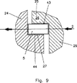
図9による詳細な表示から明らかなように、クリスタル5は2つの冷却ジョー24、25のそれぞれ段差状の凹部28、29とノーズ突起26の間にインジウムの箔43、44を介しておかれ、クリスタル5と冷却ジョー24、25の間の良好な熱伝導を得ている。
【0043】
容器8の真空排気ではなくて、後者の装備(すなわち、ペルチエ要素とレーザクリスタルの装着)をクリーンルームにすることも可能であって、それによれば、例えば、それ自体シリカゲルとして知られているような乾燥材を、例えば冷却ジョー24、25に近接して適用して、容器8をきつく閉じる。このようにしても、クリスタル5の上への粒子、凝縮された水滴の堆積を防止することができる。
【0044】
さらに、冷却装置の変形例においては、クリスタル5を上側と下側のペルチエ要素の間にサンドイッチ状に取り付ける、その外側、すなわち、クリスタル5から離れる各上側または下側において、各、例えば、プレート状の、冷却受け台が接する。
【0045】
また、多くの場合において、少なくとも、作業中に公知の方法でクリスタル5の温度を監視、好ましくは制御、することが可能であって、かつ、好適である。この目的のために、温度の監視、または、制御回路に接続された温度センサ(図示せず)を冷却ジョーの1つ、例えば、25に挿入することができる。図8Aには、穴45が示されているが、この中にそれ自体従来の温度センサを挿入するとができる。
【図面の簡単な説明】
【図1】 光学増幅器の基本部品の概略図である。
【図2】 光学増幅器に使用されるレーザクリスタル用の冷却装置の頂部構造を断面で示した上面図である。
【図3】 図2のIII-III 線に沿って見た冷却装置の軸方向断面図である。
【図4】 冷却装置と共に使用されるマウンティングと冷却受け台を示す図である。
【図5】 下部フランジ部分における冷却受け台を示す図である。
【図6】 図5のVI-VI 線に沿って見た冷却受け台のフランジ部の断面図である。
【図7A】 図2、3の冷却装置と共に使用されるレーザクリスタル用の一つの冷却ジョーの上面図である。
【図7B】 図2、3の冷却装置と共に使用されるレーザクリスタル用の一つの冷却ジョーの正面図である。
【図7C】 図2、3の冷却装置と共に使用されるレーザクリスタル用の一つの冷却ジョーの端面図である。
【図8A】 図2、3の冷却装置と共に使用されるレーザクリスタル用の別の冷却ジョーの上面図である。
【図8B】 図2、3の冷却装置と共に使用されるレーザクリスタル用の別の冷却ジョーの正面図である。
【図8C】 図2、3の冷却装置と共に使用されるレーザクリスタル用の別の冷却ジョーの端面図である。
【図9】 インジウム箔が配設された、図7、8の冷却ジョーの間のレーザクリスタルの押さえ材を拡大して詳細に示す図である。[0001]
The present invention provides a thermally loaded Peltier element for a laser beam, in particular an optical crystal from which a laser pulse is obtained, or a laser crystal, respectively, for example an optical amplifier or an oscillator laser crystal. The present invention relates to a cooling device provided.
[0002]
The cooling of the optical crystal in the laser device or the laser crystal, each of which is hereinafter simply referred to as “crystal”, is a crystal, for example, a titanium-sapphire crystal (generally referred to as Ti: S laser crystal). Is particularly important when exposed to high heat loads during operation. This is the case, for example, when crystals are used as optically non-linear elements in passively mode-locked short pulse laser devices (oscillators) When the resonator beam is focused as high as possible in the crystal, in doing so the crystal must be small in size and to compensate for it, the dispersion of the material must be low The contribution must be high to hold, which increases the specific thermal load, as described in the unpublished earlier application WO-98 / 10 494-A. It is also stated that cooling to below 10 ° C is problematic because of the condensation of moisture that occurs at that time, with the small droplets condensing on the crystal abruptly damaging or destroying the crystal. ing.
[0003]
Of particular importance is also the cooling of the crystal in the case of an optical amplifier, which has already been published in Optics Letters, Vol. 22, no. No. 16, pages 1256 to 1258, as described in the paper by Buckus et al, “0.2-TW laser system at 1 kHz”. In such an optical post-amplification of the oscillator, for example, a titanium-sapphire laser crystal is also used, where a pulse with energy of several nJ from the oscillator is amplified to the order of 1 mJ. (
[0004]
Due to the fact that the optical amplifier is activated by pulses (the pulse frequency is approximately 1 kHz), the pumping energy is concentrated in independent pulses, which amplify the oscillator pulses. Due to the high power generated there, it is important to sufficiently cool the crystal. Insufficient crystal cooling not only results in low efficiency, but also induces an unfavorable beam shape due to the “thermal lense” effect, similar to that of the oscillator, which is also mentioned in the article by Bax et al. It is stated in.
[0005]
When the crystal is heated, the resulting temperature gradient within the material induces a refractive index gradient that, depending on the crystal material, causes unintentional focusing or defocusing during the passage of the laser beam. Good cooling of the crystal improves the thermal conductivity at low temperatures, reduces the temperature coefficient of refractive index, and obtains a beam shape that corresponds to a nearly ideal Gaussian intensity profile (in cross section) Can do. Furthermore, the degree of efficiency is improved.
[0006]
According to a paper by Bax et al., Liquid nitrogen is used to cool the crystal, thereby allowing extremely low temperatures, but it can be used for many purposes, especially for mobile use. Realization of practical optical amplifiers is hampered.
[0007]
A slightly different optical amplifier is described in Optics Letters, Vol. 22, no. 20 papers by Sartania et al, "0.2-TW 5-fs optical pulse at a 1-kHz", where a Peltier cooling device is used to cool the crystal. It is outlined. However, with cooperative cooling, the problem remains that not only the water condensed on the crystal, but also ice is formed, dirt is in the air and it accumulates on the crystal. In fact, such ice formation and contamination lead to local destruction due to corrosion of the crystal surface.
[0008]
The object of the present invention is to overcome the above-mentioned drawbacks, while at the same time being suitable for particularly mobile applications, despite its simple construction, to obtain a highly efficient and good cooling and an optimum beam shape. On the other hand, it is to provide a cooling device of the type defined first, which can ensure a long life of the laser crystal by preventing the corrosion by condensed water (ice) or impurities.
[0009]
The present invention provides an optical laser crystal device. The laser crystal device comprises a laser crystal (5) and a cooling device (7) comprising a Peltier element (18) for the laser crystal. Laser crystals are in operation10 watts or moreOptical power ofofThermally loaded, laser pulses (2) are generated from the laser crystal, and the laser crystal (5) is supported between cooling jaws (24, 25) made of a material with good thermal conductivity. The laser crystal (5) is housed in a sealed container (8) together with a Peltier element (18) and cooling jaws (24, 25) provided for cooling the laser crystal. ) For the passage of a laser pulse (2) whose interior is evacuated and whose sealed container (8) is arranged at an angle with respect to the optical axis corresponding to the Brewster angle. It has at least one Brewster window (32, 33).
[0010]
By providing a sealed container, the inside of the container can be evacuated or kept dry, and condensed water does not deposit on the optical crystal or laser crystal, respectively. In addition, a clean environment (vacuum or pure, i.e. clean, dry air) defined for the crystal is possible. Long operating times can thus be obtained, which is also a great advantage in terms of consumption required during mounting of the optical crystal or laser crystal or during precise adjustment.
[0011]
Furthermore, the cooling device of the present invention enables the construction of a laser device that is compact, simple and easy to handle by using a thermoelastic cooling element, that is, a Peltier element, together with a sealed container. Furthermore, it is characterized in that it can be used in a vehicle without any problems, for example, also in an aircraft, but it reduces the influence of gravity during operation compared to cooling with liquid nitrogen. By not receiving. The container may comprise a coupling means for evacuation that can be tightly closed and a strongly sealable wire passage for supplying power to the Peltier element.
[0012]
In view of the high intensity that occurs in the application, a so-called Brewster window for the passage of a laser beam is provided in the container. In this way, i.e. without the wide-width antireflective coating that would otherwise be used, unintentional refraction can be prevented. This is because such a dielectric coating cannot withstand the high strengths mentioned above (eg, beam diameter is less than 10 mm, peak power ranges from MW to GW and pulse duration from 10 fs to ps). The average output is in the range from 10 mW to W, and the pump parameters range from several W to several tens W, the pump energy is several mJ, and the high repetition frequency is in the kHz range. Lead the output to the range of MW to GW).
[0013]
For semiconductor lasers it is known to use sealed modules, see for example German Patent DE 3307933C, German Patent DE 3922800A, Japanese Patent Publication JP 1-122183A, or European Patent EP 259888A, where a laser with a Peltier element. A diode element is shown. However, there is no high laser power, the laser diode element has a low thermal load, and the Peltier element is actually only used for temperature stabilization purposes. This is important in known semiconductor lasers, since in the case of laser diodes the laser wavelength basically depends on the temperature of the semiconductor chip and in many cases even heating is required to obtain the correct wavelength. .
Furthermore, these known devices do not mention evacuation or drying of the module with a desiccant.
[0014]
It has been shown that with Peltier elements, sufficient cooling of the laser crystal can often be achieved without any problems, and in many cases a temperature difference of 50-70 ° C. in the Peltier element is sufficient. For particularly noticeable heat dissipation from the laser crystal or cooling, it is advantageous to provide a stack of Peltier elements. In this case, when the heat side is the atmospheric temperature (about 20 ° C.), it is easy to obtain −50 to −100 ° C. on the cold side. As described above, when the conventional Peltier element is used, a temperature difference of the Peltier element reaching 130 ° C. can be obtained, and cooling at −100 ° C. or less can be performed.
[0015]
Each optical crystal or laser crystal is shaped into a platelet and has relatively small dimensions to obtain good cooling and is about 3 mm wide and long when used with an amplifier. The height is only 1 to 1.5 mm.
[0016]
In order to secure the crystal while ensuring a good heat transfer and heat dissipation, it is advantageous to place the crystal between a good thermally conductive cooling jaw on which the Peltier element is placed. In so doing, it is preferred that the cooling jaws actually hold the crystal from four sides in order to obtain as large a heat transfer surface as possible, as well as a particularly simple crystal hold.
[0017]
A preferred solution in terms of manufacturing and mounting is further that a nose protrusion in which one of the two cooling jaws resting on the opposite side of the crystal extends over the crystal resting on the other cooling jaw. And the cooling jaw is provided with a recess for passing the laser beam in the direction of the laser beam before and after the crystal.
[0018]
Keeping the “hot” side of the Peltier element at ambient temperature (or even lower) is even more advantageous when the Peltier element is engaged with the cooling cradle on the heat side away from the cooling jaws. It has been found that it is advantageous to liquid cool the cooling cradle to efficiently cool the hot side of the Peltier element. The cooling cradle may have any shape, for example, a cubic shape or a disk shape. In order to obtain a high cooling storage capacity and to make it easy for the stable harmony of the Peltier elements and the cooling jaws, the cooling cradle is fitted with a crystal at the end to match the Peltier elements and the cooling jaws to the crystal. More preferably, it is formed in a substantially cylindrical shape having a letter-shaped recess.
[0019]
For process reasons and also for the receiving surface of the Peltier element, it is advantageous for the V-shaped recess to have an apex angle of 90 °. In order to orient the Peltier element and to facilitate its mounting, the V-shaped recesses further define an inclined mounting surface for the Peltier element, from the mounting surface for the Peltier element It is advantageous to provide an upwardly protruding stop at the inner end adjacent to the mounting surface.
[0020]
When the container is provided with a cylindrical casing that is closed with a lid, for example, an O-ring can provide a sealed type container with a particularly simple design that can provide a good seal. In this regard, it is further advantageous to provide the cooling cradle with a flange capable of strongly coupling the tubular casing on the end facing away from the Peltier element. It is also advantageous if the cooling cradle is provided with a hole through which the cooling liquid passes in the region of the flange.
[0021]
In order for the laser beam to have a relatively low power per unit area (so as not to cause window corrosion and destruction in a short operating time) as it passes through the window, the laser beam is It is necessary to have as wide a cross-section as possible, i.e. out of focus, which means that the window must be separated from the crystal by some distance (e.g. about 8-10 cm). In order to make this possible without enlarging the entire container, the sealed container is preferably closed on its opposite side with a protruding, strongly attached, outer end closed with a window for the laser beam to pass through. Preferably, a pipe socket is provided.
The present invention also relates to a laser device provided with the above-described cooling device.
[0022]
Hereinafter, the details of the present invention will be described by way of exemplary embodiments shown in the drawings, but the present invention is not limited thereto.
In the following, the cooling device according to the present invention will be described in more detail with an optical amplifier by way of example as schematically illustrated in FIG. Although the cooling device has particular advantages in optical amplifiers due to efficient cooling effects, it can also be used in other laser devices, such as those with an oscillator. In addition, the materials shown below for the optical crystal or laser crystal, respectively, are (titanium-sapphire crystal), pump laser (doubled frequency Nd-YLF laser, Niodym-yttrium), respectively. Together with what has been shown for the (lithium-fluorine laser) structure, it is merely an example.
[0023]
FIG. 1 schematically shows an apparatus of the basic components of an optical amplifier, in which the optical amplifier is shown as a so-called “multipath amplifier” in the example shown. See the above-mentioned paper by Bax et al., “0.2-TW laser system at 1 kHz”. The present invention is, of course, another optical amplifier, i.e. a so-called colinear path of the laser beam that is repeated, e.g., before the laser beam exits the amplifier, e.g. by Pockels cells. It can also be applied to regenerative amplifiers.
[0024]
Specifically, in FIG. 1 a pump laser, for example a Nd-YLF laser with a doubled frequency, is shown schematically at 1 for the laser pulse shown at 2 in FIG. A laser beam for supplying energy, a so-called pump beam, is output. 3, these laser pulses are supplied to the amplifier device itself, indicated generally at 4, by a conventional laser oscillator (not shown) not shown in detail. The basic element for this amplifier device 4 is simply referred to as a crystal hereinafter, for example an optical crystal such as a Ti: S crystal or a
[0025]
Furthermore, in FIG. 1, rear reflectors for amplifying the beam are indicated by R1, R2, which provide various multipass-positions of the laser beam in space, The reflectors R1 are further arranged at predetermined intervals from each other, so that the laser pulses arriving from the oscillator enter the amplifier device 4 through a gap formed accordingly. An aperture A consisting of 4, 6 or 8 holes is then placed in front of the rear reflector R1 to suppress the activity of the laser in the amplifier 4 and the mirror 6 is decoupled with enhanced laser pulses. Is provided to do. The enhanced laser pulse P is supplied to a compressor not shown in detail because it is known per se, in which the laser pulse is shortened with respect to its duration.
[0026]
For optical amplification, a
[0027]
For further information on this point, see the “Generation of 0.1-TW 5-fs optical pulse at a 1-kHz repetition rate” of Sultania, or the “0.2-TW laser system” of Bax et al. Reference can be made to “at 1 kHz”. For a better understanding, it should be noted that, for example, a laser pulse arriving from an oscillator has a frequency of 75 MHz and only passes every 75000 pulses and is augmented with energy from the pump laser. is there.
[0028]
In view of the high power that the pump pulse has, as well as the focus of the pump pulse in a relatively small crystal volume, a correspondingly high amount of heat is generated there and efficient cooling of the crystal is very important. Furthermore, from the point of industrial application of amplifiers or laser devices, cooling with liquid nitrogen, as in known devices, is not suitable, cumbersome and even subject to gravity. Not suitable for mobility use.
[0029]
Hereinafter, the cooling device shown as a whole by 7 will be described with reference to FIGS. 2 to 9. This cooling device fulfills various requirements such as sufficient cooling, compactness, simple, easy-to-handle structure, not influenced by gravity, and so on. The feature is that the crystal can be used for a long time.
[0030]
As can be seen from FIGS. 2 and 3, the cooling device 7 comprises a sealed container type, tightly closed
[0031]
As is particularly apparent from FIGS. 5 and 6, the cooling
The cooling
[0032]
From the bottom of the cooling
[0033]
In the illustrated exemplary embodiment, two blocks of Peltier elements are each stacked on both mounting
[0034]
As clearly shown in the front views of FIGS. 7B and 8B, the cooling
[0035]
As is apparent from the top view of the cooling
[0036]
Similarly, and in the imaginary extension of the nose projection, the cooling
[0037]
The depth T of the
[0038]
As described above, the stepped recesses 28 and 29 of the cooling
[0039]
For passage of the
[0040]
The slightly
[0041]
In order to evacuate the
[0042]
As is clear from the detailed representation according to FIG. 9, the
[0043]
Rather than evacuating the
[0044]
Furthermore, in a variant of the cooling device, the
[0045]
Also, in many cases, it is possible and suitable to monitor, preferably control, the temperature of the
[Brief description of the drawings]
FIG. 1 is a schematic diagram of basic components of an optical amplifier.
FIG. 2 is a top view showing in cross section the top structure of a cooling device for a laser crystal used in an optical amplifier.
3 is an axial cross-sectional view of the cooling device taken along line III-III in FIG. 2;
FIG. 4 is a view showing a mounting and a cooling cradle used together with a cooling device.
FIG. 5 is a view showing a cooling cradle in a lower flange portion.
6 is a cross-sectional view of the flange portion of the cooling cradle as seen along line VI-VI in FIG.
7A is a top view of one cooling jaw for a laser crystal used with the cooling device of FIGS.
7B is a front view of one cooling jaw for a laser crystal used with the cooling device of FIGS.
7C is an end view of one cooling jaw for a laser crystal used with the cooling device of FIGS.
8A is a top view of another cooling jaw for a laser crystal used with the cooling device of FIGS.
8B is a front view of another cooling jaw for a laser crystal used with the cooling device of FIGS.
8C is an end view of another cooling jaw for a laser crystal used with the cooling device of FIGS.
FIG. 9 is an enlarged detail view showing a laser crystal holding member between the cooling jaws of FIGS. 7 and 8 in which an indium foil is disposed.
Claims (13)
レーザクリスタル(5)と、該レーザクリスタルのためのペルチエ要素(18)を含む冷却装置(7)とを具備する、レーザクリスタル装置において、
前記レーザクリスタルは、稼動において、10ワット以上の光学的動力の熱的に高い負荷がかけられており、前記レーザクリスタルからレーザパルス(2)が生得されており、
前記レーザクリスタル(5)が熱伝導性の良い材料から成る冷却ジョー(24、25)の間に支持されており、
前記レーザクリスタル(5)は、前記レーザクリスタルを冷却するために備えられる前記ペルチエ要素(18)及び前記冷却ジョー(24、25)と共に、密封容器(8)に収容されており、
前記密封容器(8)は、その内部が真空排気されており、更に
前記密封容器(8)が、ブリュースター角に対応する光学軸に対して角度を成して配設された前記レーザパルス(2)の通過のための少なくとも1つのブリュースター窓(32、33)を有していることを特徴とするレーザクリスタル装置。An optical laser crystal device,
In a laser crystal device comprising a laser crystal (5) and a cooling device (7) comprising a Peltier element (18) for the laser crystal,
The laser crystal is thermally loaded with an optical power of 10 watts or more in operation, and a laser pulse (2) is generated from the laser crystal,
The laser crystal (5) is supported between cooling jaws (24, 25) made of a material having good thermal conductivity,
The laser crystal (5) is housed in a sealed container (8) together with the Peltier element (18) and the cooling jaws (24, 25) provided for cooling the laser crystal,
The sealed container (8) is evacuated in its interior, and the sealed container (8) is arranged such that the laser pulse (8) disposed at an angle with respect to the optical axis corresponding to the Brewster angle. Laser crystal device characterized in that it has at least one Brewster window (32, 33) for the passage of 2).
Applications Claiming Priority (3)
| Application Number | Priority Date | Filing Date | Title |
|---|---|---|---|
| AT1992/97 | 1997-11-24 | ||
| AT0199297A AT405776B (en) | 1997-11-24 | 1997-11-24 | COOLING DEVICE FOR A LASER CRYSTAL |
| PCT/AT1998/000256 WO1999027621A1 (en) | 1997-11-24 | 1998-10-22 | Cooling device for an optical crystal or laser crystal |
Related Child Applications (1)
| Application Number | Title | Priority Date | Filing Date |
|---|---|---|---|
| JP2010099210A Division JP4741707B2 (en) | 1997-11-24 | 2010-04-22 | Cooling device for optical crystal or laser crystal, respectively |
Publications (2)
| Publication Number | Publication Date |
|---|---|
| JP2001524761A JP2001524761A (en) | 2001-12-04 |
| JP4643003B2 true JP4643003B2 (en) | 2011-03-02 |
Family
ID=3525504
Family Applications (2)
| Application Number | Title | Priority Date | Filing Date |
|---|---|---|---|
| JP2000522654A Expired - Fee Related JP4643003B2 (en) | 1997-11-24 | 1998-10-22 | Cooling device for optical crystal or laser crystal, respectively |
| JP2010099210A Expired - Fee Related JP4741707B2 (en) | 1997-11-24 | 2010-04-22 | Cooling device for optical crystal or laser crystal, respectively |
Family Applications After (1)
| Application Number | Title | Priority Date | Filing Date |
|---|---|---|---|
| JP2010099210A Expired - Fee Related JP4741707B2 (en) | 1997-11-24 | 2010-04-22 | Cooling device for optical crystal or laser crystal, respectively |
Country Status (7)
| Country | Link |
|---|---|
| US (2) | US6625184B1 (en) |
| EP (1) | EP1034584B1 (en) |
| JP (2) | JP4643003B2 (en) |
| AT (1) | AT405776B (en) |
| AU (1) | AU737909B2 (en) |
| DE (1) | DE59801270D1 (en) |
| WO (1) | WO1999027621A1 (en) |
Families Citing this family (20)
| Publication number | Priority date | Publication date | Assignee | Title |
|---|---|---|---|---|
| EP1196969B1 (en) * | 1999-07-02 | 2003-04-23 | Asah Medico A/S | A solid-state laser crystal assembly |
| JP2004253733A (en) * | 2003-02-21 | 2004-09-09 | Topcon Corp | Semiconductor laser device and laser crystal holding method for semiconductor laser device |
| EP1519039A1 (en) * | 2003-09-23 | 2005-03-30 | AVL List GmbH | Q-switched pumped solid-state laser |
| JP4627445B2 (en) * | 2005-02-23 | 2011-02-09 | 浜松ホトニクス株式会社 | Laser amplifier |
| US20060239304A1 (en) * | 2005-04-23 | 2006-10-26 | Photonics Industries Int'l | High powered TEM00 mode pulsed laser |
| JP2008042061A (en) * | 2006-08-09 | 2008-02-21 | National Institute Of Advanced Industrial & Technology | Laser regenerative amplifier |
| AT506455B1 (en) | 2008-02-18 | 2011-10-15 | Femtolasers Produktions Gmbh | LASER CRYSTAL DEVICE |
| DE102008029423B4 (en) * | 2008-06-23 | 2010-12-30 | Trumpf Laser Gmbh + Co. Kg | Laser, in particular disk laser with optical overheating monitoring of the laser disk |
| US20090323287A1 (en) * | 2008-06-25 | 2009-12-31 | Joseph Martin Patterson | Integrated Circuit Cooling Apparatus for Focused Beam Processes |
| CN101656392B (en) * | 2009-09-11 | 2011-05-04 | 天津大学 | Cooling device for resisting heat distortion for laser crystal and implementation method |
| US8605355B2 (en) * | 2009-11-24 | 2013-12-10 | Applied Energetics | Off axis walk off multi-pass amplifiers |
| DE102010036286A1 (en) * | 2010-08-31 | 2012-03-01 | Friedrich-Schiller-Universität Jena | Method and apparatus for thermal stabilization of a rare earth laser with reduced cooling and thermal degradation |
| CN102544994B (en) * | 2011-04-21 | 2014-06-11 | 北京国科世纪激光技术有限公司 | Heat sink device |
| GB201200219D0 (en) * | 2012-01-09 | 2012-02-22 | Calder Martin | A clock signal generator for a digital circuit |
| US10794667B2 (en) * | 2017-01-04 | 2020-10-06 | Rolls-Royce Corporation | Optical thermal profile |
| US10811835B2 (en) | 2017-02-16 | 2020-10-20 | University Of Pittsburgh-Of The Commonwealth System Of Higher Education | Laser system enabled by additive manufacturing |
| CN109411997B (en) * | 2018-11-08 | 2019-12-20 | 中国科学院上海光学精密机械研究所 | Laminated repetition frequency sheet amplifier for xenon lamp pumping liquid cooling |
| CN116742452B (en) * | 2023-07-05 | 2024-04-05 | 深圳市格镭激光科技有限公司 | Water-cooled solid laser |
| CN116914537B (en) * | 2023-07-14 | 2025-09-26 | 河南省启封新源光电科技有限公司 | A water-cooled gain medium and a crystal fixture for suppressing lateral parasitic oscillation |
| CN117154509B (en) * | 2023-09-11 | 2024-06-14 | 如东盛晖激光科技有限公司 | Carbon dioxide laser with lens cooling protection function |
Family Cites Families (27)
| Publication number | Priority date | Publication date | Assignee | Title |
|---|---|---|---|---|
| US2858654A (en) * | 1952-08-05 | 1958-11-04 | Jr Edward B Westlake | Method of producing desiccant container |
| US3142830A (en) * | 1961-07-20 | 1964-07-28 | Alpha Res And Dev Inc | Desiccant container with desiccant saturation indicator |
| US3621273A (en) * | 1970-03-05 | 1971-11-16 | Coherent Radiation | Optical second harmonic generator |
| JPS5113639B2 (en) * | 1972-04-28 | 1976-05-01 | ||
| US4119195A (en) * | 1975-05-19 | 1978-10-10 | Widener Charles D | Protective case |
| DE3307933C2 (en) * | 1983-03-05 | 1987-05-07 | ANT Nachrichtentechnik GmbH, 7150 Backnang | Optoelectronic transmitter unit |
| JPS59197186A (en) * | 1983-04-25 | 1984-11-08 | Canon Inc | semiconductor equipment |
| JPS6062172A (en) * | 1983-09-16 | 1985-04-10 | Mitsubishi Electric Corp | Moisture removal device for laser oscillator |
| DE8433460U1 (en) * | 1984-11-15 | 1985-03-21 | Gerhardt, Harald, Dr., 3012 Langenhagen | GAS LASER PIPE |
| US4787088A (en) * | 1985-03-20 | 1988-11-22 | Fuji Photo Film Co., Ltd. | Semiconductor laser beam source apparatus |
| JPS6370589A (en) * | 1986-09-12 | 1988-03-30 | Nec Corp | Semiconductor laser module |
| JPS6472576A (en) * | 1987-09-11 | 1989-03-17 | Mitsubishi Electric Corp | Solid-state laser device |
| US4827484A (en) * | 1987-10-14 | 1989-05-02 | Melles Griot San Marcos Company | Apparatus and method for suppressing diffraction rings in a laser |
| JPH01122183A (en) * | 1987-11-06 | 1989-05-15 | Hitachi Ltd | Semiconductor laser device |
| JPH02156583A (en) * | 1988-12-09 | 1990-06-15 | Asahi Glass Co Ltd | Laser diode excitation solid-state laser |
| DE3922800A1 (en) * | 1989-07-11 | 1991-01-17 | Siemens Ag | LASER DIODE TRANSMITTER WITH COMMERCIAL LASER MODULE |
| JP2551109Y2 (en) * | 1991-04-26 | 1997-10-22 | ホーヤ株式会社 | Multi-frequency laser light source device |
| US5166943A (en) * | 1991-06-14 | 1992-11-24 | Amoco Corporation | Single domain stabilization in ferroelectric crystals |
| JPH0572577A (en) * | 1991-09-11 | 1993-03-26 | Hitachi Ltd | Non-linear optical crystal holder |
| JP3480946B2 (en) * | 1992-02-20 | 2003-12-22 | ソニー株式会社 | Laser light generator |
| DE4229500A1 (en) * | 1992-09-04 | 1994-03-10 | Deutsche Aerospace | Solid-state hybrid laser system - with laser diode chip and associated cooling and temp. regulation elements contained in standard housing |
| JPH06338569A (en) | 1993-05-31 | 1994-12-06 | Mitsubishi Electric Corp | Package for semiconductor optical device |
| US5495489A (en) * | 1994-05-07 | 1996-02-27 | Samsung Electronics Co., Ltd. | Second harmonic generating method and apparatus |
| US5696785A (en) * | 1994-10-11 | 1997-12-09 | Corning Incorporated | Impurity getters in laser enclosures |
| JPH08204261A (en) * | 1995-01-25 | 1996-08-09 | Toshiba Seiki Kk | Laser equipment |
| JPH0955551A (en) * | 1995-08-14 | 1997-02-25 | Nec Corp | Solid state laser |
| JPH0983048A (en) * | 1995-09-14 | 1997-03-28 | Nec Corp | Solid state laser |
-
1997
- 1997-11-24 AT AT0199297A patent/AT405776B/en active
-
1998
- 1998-10-22 AU AU96155/98A patent/AU737909B2/en not_active Ceased
- 1998-10-22 US US09/555,087 patent/US6625184B1/en not_active Expired - Lifetime
- 1998-10-22 WO PCT/AT1998/000256 patent/WO1999027621A1/en not_active Ceased
- 1998-10-22 JP JP2000522654A patent/JP4643003B2/en not_active Expired - Fee Related
- 1998-10-22 DE DE59801270T patent/DE59801270D1/en not_active Expired - Lifetime
- 1998-10-22 EP EP98949819A patent/EP1034584B1/en not_active Expired - Lifetime
-
2003
- 2003-08-08 US US10/637,785 patent/US7039081B2/en not_active Expired - Fee Related
-
2010
- 2010-04-22 JP JP2010099210A patent/JP4741707B2/en not_active Expired - Fee Related
Also Published As
| Publication number | Publication date |
|---|---|
| JP2001524761A (en) | 2001-12-04 |
| EP1034584B1 (en) | 2001-08-22 |
| US7039081B2 (en) | 2006-05-02 |
| AU9615598A (en) | 1999-06-15 |
| JP2010171459A (en) | 2010-08-05 |
| US6625184B1 (en) | 2003-09-23 |
| ATA199297A (en) | 1999-03-15 |
| AU737909B2 (en) | 2001-09-06 |
| EP1034584A1 (en) | 2000-09-13 |
| WO1999027621A1 (en) | 1999-06-03 |
| AT405776B (en) | 1999-11-25 |
| DE59801270D1 (en) | 2001-09-27 |
| US20050175049A1 (en) | 2005-08-11 |
| JP4741707B2 (en) | 2011-08-10 |
Similar Documents
| Publication | Publication Date | Title |
|---|---|---|
| JP4741707B2 (en) | Cooling device for optical crystal or laser crystal, respectively | |
| US7535633B2 (en) | Laser amplifiers with high gain and small thermal aberrations | |
| US6307871B1 (en) | Laser system using phase change material for thermal control | |
| JP3155132B2 (en) | Solid-state laser device and laser processing device | |
| US6134258A (en) | Transverse-pumped sLAB laser/amplifier | |
| US7852886B2 (en) | Reduction of surface heating effects in nonlinear crystals for high power frequency conversion of laser light | |
| US6351478B1 (en) | Passively cooled solid-state laser | |
| DK2652844T3 (en) | Laser amplification module and manufacturing method | |
| WO2006070548A1 (en) | Solid laser module, optical amplifier, and laser oscillator | |
| JP2004363129A (en) | Optical crystal holder, solid-state laser system, method of fixing optical crystal, and structure and method for positioning solid-state laser crystal | |
| JP5424320B2 (en) | Solid state laser equipment | |
| JPH05198870A (en) | Semiconductor laser pumping solid laser equipment | |
| JPH02161786A (en) | Semiconductor laser excitation solid laser device | |
| EP1618633B1 (en) | Laser apparatus for generating a visible laser beam | |
| JP2012033818A (en) | Semiconductor laser-excited solid-state laser apparatus | |
| JP2005217090A (en) | Plate type body cooling structure and laser oscillator | |
| CN114204385A (en) | Solid state laser device | |
| JPH11223843A (en) | Crystal holding device | |
| JPH0525261Y2 (en) | ||
| JPH01289180A (en) | Solid state laser | |
| Kiriyama et al. | Design and operation of high-energy and high-average-power diode-pumped single Nd: YAG amplifier with stimulated-brillouion-scattering phase conjugate mirror | |
| JPH0730171A (en) | Semiconductor laser-excited solid-state laser device | |
| Yakshin et al. | Compact, high brightness and high repetition rate side-diode-pumped Yb: YAG Laser | |
| JPH0730172A (en) | Semiconductor laser-excited solid-state laser device |
Legal Events
| Date | Code | Title | Description |
|---|---|---|---|
| A621 | Written request for application examination |
Free format text: JAPANESE INTERMEDIATE CODE: A621 Effective date: 20051013 |
|
| A131 | Notification of reasons for refusal |
Free format text: JAPANESE INTERMEDIATE CODE: A131 Effective date: 20071127 |
|
| A601 | Written request for extension of time |
Free format text: JAPANESE INTERMEDIATE CODE: A601 Effective date: 20080226 |
|
| A602 | Written permission of extension of time |
Free format text: JAPANESE INTERMEDIATE CODE: A602 Effective date: 20080304 |
|
| A521 | Request for written amendment filed |
Free format text: JAPANESE INTERMEDIATE CODE: A523 Effective date: 20080516 |
|
| A131 | Notification of reasons for refusal |
Free format text: JAPANESE INTERMEDIATE CODE: A131 Effective date: 20081111 |
|
| A601 | Written request for extension of time |
Free format text: JAPANESE INTERMEDIATE CODE: A601 Effective date: 20090210 |
|
| A602 | Written permission of extension of time |
Free format text: JAPANESE INTERMEDIATE CODE: A602 Effective date: 20090218 |
|
| A521 | Request for written amendment filed |
Free format text: JAPANESE INTERMEDIATE CODE: A523 Effective date: 20090417 |
|
| A02 | Decision of refusal |
Free format text: JAPANESE INTERMEDIATE CODE: A02 Effective date: 20091222 |
|
| A521 | Request for written amendment filed |
Free format text: JAPANESE INTERMEDIATE CODE: A523 Effective date: 20100422 |
|
| A521 | Request for written amendment filed |
Free format text: JAPANESE INTERMEDIATE CODE: A523 Effective date: 20100507 |
|
| A911 | Transfer to examiner for re-examination before appeal (zenchi) |
Free format text: JAPANESE INTERMEDIATE CODE: A911 Effective date: 20100528 |
|
| A131 | Notification of reasons for refusal |
Free format text: JAPANESE INTERMEDIATE CODE: A131 Effective date: 20100824 |
|
| A521 | Request for written amendment filed |
Free format text: JAPANESE INTERMEDIATE CODE: A523 Effective date: 20101008 |
|
| TRDD | Decision of grant or rejection written | ||
| A01 | Written decision to grant a patent or to grant a registration (utility model) |
Free format text: JAPANESE INTERMEDIATE CODE: A01 Effective date: 20101102 |
|
| A01 | Written decision to grant a patent or to grant a registration (utility model) |
Free format text: JAPANESE INTERMEDIATE CODE: A01 |
|
| A61 | First payment of annual fees (during grant procedure) |
Free format text: JAPANESE INTERMEDIATE CODE: A61 Effective date: 20101202 |
|
| R150 | Certificate of patent or registration of utility model |
Free format text: JAPANESE INTERMEDIATE CODE: R150 |
|
| FPAY | Renewal fee payment (event date is renewal date of database) |
Free format text: PAYMENT UNTIL: 20131210 Year of fee payment: 3 |
|
| R250 | Receipt of annual fees |
Free format text: JAPANESE INTERMEDIATE CODE: R250 |
|
| R250 | Receipt of annual fees |
Free format text: JAPANESE INTERMEDIATE CODE: R250 |
|
| R250 | Receipt of annual fees |
Free format text: JAPANESE INTERMEDIATE CODE: R250 |
|
| R250 | Receipt of annual fees |
Free format text: JAPANESE INTERMEDIATE CODE: R250 |
|
| LAPS | Cancellation because of no payment of annual fees |