JP4637694B2 - Power factor correction circuit and output voltage control method thereof - Google Patents
Power factor correction circuit and output voltage control method thereof Download PDFInfo
- Publication number
- JP4637694B2 JP4637694B2 JP2005262523A JP2005262523A JP4637694B2 JP 4637694 B2 JP4637694 B2 JP 4637694B2 JP 2005262523 A JP2005262523 A JP 2005262523A JP 2005262523 A JP2005262523 A JP 2005262523A JP 4637694 B2 JP4637694 B2 JP 4637694B2
- Authority
- JP
- Japan
- Prior art keywords
- voltage
- output
- input
- reference voltage
- boost circuit
- Prior art date
- Legal status (The legal status is an assumption and is not a legal conclusion. Google has not performed a legal analysis and makes no representation as to the accuracy of the status listed.)
- Expired - Fee Related
Links
Images
Classifications
-
- G—PHYSICS
- G05—CONTROLLING; REGULATING
- G05F—SYSTEMS FOR REGULATING ELECTRIC OR MAGNETIC VARIABLES
- G05F1/00—Automatic systems in which deviations of an electric quantity from one or more predetermined values are detected at the output of the system and fed back to a device within the system to restore the detected quantity to its predetermined value or values, i.e. retroactive systems
- G05F1/70—Regulating power factor; Regulating reactive current or power
-
- H—ELECTRICITY
- H02—GENERATION; CONVERSION OR DISTRIBUTION OF ELECTRIC POWER
- H02M—APPARATUS FOR CONVERSION BETWEEN AC AND AC, BETWEEN AC AND DC, OR BETWEEN DC AND DC, AND FOR USE WITH MAINS OR SIMILAR POWER SUPPLY SYSTEMS; CONVERSION OF DC OR AC INPUT POWER INTO SURGE OUTPUT POWER; CONTROL OR REGULATION THEREOF
- H02M1/00—Details of apparatus for conversion
- H02M1/42—Circuits or arrangements for compensating for or adjusting power factor in converters or inverters
- H02M1/4208—Arrangements for improving power factor of AC input
- H02M1/4225—Arrangements for improving power factor of AC input using a non-isolated boost converter
-
- Y—GENERAL TAGGING OF NEW TECHNOLOGICAL DEVELOPMENTS; GENERAL TAGGING OF CROSS-SECTIONAL TECHNOLOGIES SPANNING OVER SEVERAL SECTIONS OF THE IPC; TECHNICAL SUBJECTS COVERED BY FORMER USPC CROSS-REFERENCE ART COLLECTIONS [XRACs] AND DIGESTS
- Y02—TECHNOLOGIES OR APPLICATIONS FOR MITIGATION OR ADAPTATION AGAINST CLIMATE CHANGE
- Y02B—CLIMATE CHANGE MITIGATION TECHNOLOGIES RELATED TO BUILDINGS, e.g. HOUSING, HOUSE APPLIANCES OR RELATED END-USER APPLICATIONS
- Y02B70/00—Technologies for an efficient end-user side electric power management and consumption
- Y02B70/10—Technologies improving the efficiency by using switched-mode power supplies [SMPS], i.e. efficient power electronics conversion e.g. power factor correction or reduction of losses in power supplies or efficient standby modes
Landscapes
- Engineering & Computer Science (AREA)
- Power Engineering (AREA)
- Physics & Mathematics (AREA)
- Electromagnetism (AREA)
- General Physics & Mathematics (AREA)
- Radar, Positioning & Navigation (AREA)
- Automation & Control Theory (AREA)
- Rectifiers (AREA)
- Dc-Dc Converters (AREA)
Description
本発明は、力率補正回路及びその出力電圧制御方法に関し、特に入力電圧に応じて出力電圧が変化する力率補正回路及びその出力電圧制御方法に関する。 The present invention relates to a power factor correction circuit and an output voltage control method thereof, and more particularly to a power factor correction circuit in which an output voltage changes according to an input voltage and an output voltage control method thereof.
最近、雑音規制が厳しくなり、IEC規格EN61000−3−2のような高調波電流規制を受けて、大部分のスイッチングモードパワーサプライ(スイッチング型電源装置:SMPS)に力率補正回路を使用している。SMPSは、入力される交流供給電圧を一つ以上の直流出力電圧に変換する装置であって、移動電話、ラップトップコンピュータなどのような直流電力供給装置に主に使用される。このようなSMPSで、入力電流が入力電圧に追従して、力率を補正する力率補正回路が使用される。つまり、力率補正回路は、外部から印加される交流入力電圧に入力電流が追従できるようにすると同時に、入力される交流電圧を一定の直流電圧に変換して出力する回路である。 Recently, noise regulations have become stricter, and due to harmonic current restrictions such as IEC standard EN61000-3-2, power factor correction circuits are used in most switching mode power supplies (switching type power supply devices: SMPS). Yes. The SMPS is a device that converts an input AC supply voltage into one or more DC output voltages, and is mainly used in a DC power supply device such as a mobile phone or a laptop computer. In such SMPS, a power factor correction circuit that corrects a power factor by using an input current following an input voltage is used. That is, the power factor correction circuit is a circuit that allows an input current to follow an AC input voltage applied from the outside, and simultaneously converts the input AC voltage into a constant DC voltage and outputs the same.
大部分の力率補正回路は、ブースト回路を主に使用している。一般家庭に供給される交流電源は、100/110Vacと200/220Vacが多いため、力率補正回路は85Vacから265Vac範囲までの広い入力範囲で動作するように設計される。一方、力率補正回路として用いるブースト回路は、出力電圧が入力電圧より高電圧に設計されるべきであり、入力電圧が85Vac乃至256Vacの場合に動作させるためには、出力電圧が400Vdc程度にする必要がある。しかし、入力電圧が低い場合に出力電圧が400Vのように高電圧に設計されると、不要なスイッチング損失が発生する。力率補正回路でスイッチが遮断される場合、スイッチにかかる電圧は出力電圧になるが、このような出力電圧が低入力電圧の場合にも高電圧(つまり、400Vdc)に設定される場合には、スイッチに不要なスイッチング損失が発生する。このような問題を解決するために、出力電圧を入力電圧に合わせて変化させる方法を、通常の力率補正回路は採択している。 Most power factor correction circuits mainly use a boost circuit. Since there are many 100/110 Vac and 200/220 Vac AC power supplies supplied to ordinary households, the power factor correction circuit is designed to operate in a wide input range from 85 Vac to 265 Vac. On the other hand, the boost circuit used as the power factor correction circuit should be designed so that the output voltage is higher than the input voltage. In order to operate when the input voltage is 85 Vac to 256 Vac, the output voltage is about 400 Vdc. There is a need. However, when the input voltage is low and the output voltage is designed to be as high as 400V, unnecessary switching loss occurs. When the switch is cut off by the power factor correction circuit, the voltage applied to the switch becomes the output voltage. However, when such an output voltage is set to a high voltage (that is, 400 Vdc) even when the output voltage is low. Unnecessary switching loss occurs in the switch. In order to solve such a problem, a normal power factor correction circuit adopts a method of changing the output voltage in accordance with the input voltage.
出力電圧を入力電圧に合わせて変化させる従来の方法としては、特許文献1と特許文献2などがある。特許文献1は、入力される入力電圧のピークを検出して、出力電圧と比較される基準電圧を変化させて、出力電圧が入力電圧に合わせて変化するようにする。一方、特許文献2は、入力電圧の範囲に合わせて出力電圧を二つにする方法を採択している。つまり、入力電圧が85Vac乃至150Vacである場合には、出力電圧を220Vdcに設定し、入力電圧が150Vac乃至265Vacである場合には、出力電圧を400Vdcに設定する。 Conventional methods for changing the output voltage in accordance with the input voltage include Patent Document 1 and Patent Document 2. Patent Document 1 detects a peak of an input voltage that is input and changes a reference voltage to be compared with the output voltage so that the output voltage changes in accordance with the input voltage. On the other hand, Patent Document 2 adopts a method of making two output voltages in accordance with the input voltage range. That is, when the input voltage is 85 Vac to 150 Vac, the output voltage is set to 220 Vdc, and when the input voltage is 150 Vac to 265 Vac, the output voltage is set to 400 Vdc.
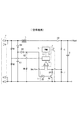
図1は、従来の力率補正回路を示す図であり、特許文献2の図1に同じ部品符号を用いて記載されている。 FIG. 1 is a diagram showing a conventional power factor correction circuit, which is described in FIG.
図1に示したように、入力電圧が85Vac乃至150Vacである場合には、ツェナーダイオード(ZD)の閾電圧を越えないため、遮断されてトランジスタ(Q1)が作動しない。従って、比較器5Aの逆相端子(−)に入力される電圧は、出力電圧(Vout)が抵抗6及び抵抗7によって分配されて、出力電圧が220Vdcに設定される。
As shown in FIG. 1, when the input voltage is 85 Vac to 150 Vac, the threshold voltage of the Zener diode (ZD) is not exceeded, so that the transistor (Q1) is not operated. Therefore, the voltage input to the negative phase terminal (−) of the
しかし、入力電圧が150Vac乃至265Vacである場合には、ツェナーダイオード(ZD)の閾電圧を越えるようになって導通し、トランジスタ(Q1)が作動する。従って、比較器5Aの逆相端子(−)に入力される電圧は、出力電圧が抵抗6、抵抗7及び抵抗(R7)によって分配されて減少することによって、出力電圧が400Vdcに設定される。
However, when the input voltage is 150Vac to 265Vac, the transistor (Q1) is activated by exceeding the threshold voltage of the Zener diode (ZD). Accordingly, the output voltage of the voltage input to the negative phase terminal (−) of the
しかし、図1に示したように、特許文献2の力率補正回路は、出力電圧を入力電圧に応じて変化させるため、入力電圧をセンシングするために、多くの外付け素子(D1、C1、D3、C2、R6、ZD、Q1、R7)を要し、そのために多額の費用が発生する。また、特許文献1の場合も、入力電圧をセンシングするために多くの外部素子が必要になって多くの費用がかかる。
本発明の目的は、前記従来技術の問題点を解決するため、簡単に入力電圧をセンシングして出力電圧を変化させる力率補正回路及びその出力電圧制御方法を提供することである。 An object of the present invention is to provide a power factor correction circuit that easily senses an input voltage and changes an output voltage, and an output voltage control method thereof, in order to solve the problems of the prior art.
前記目的を達成するための本発明の特徴による力率補正回路は、入力端に結合されるスイッチを含み、前記スイッチの動作によって出力端に出力電圧を供給するブースト回路;及び前記ブースト回路の入力端に交流入力電圧が入力された後、前記ブースト回路の入力端に交流入力電圧が入力されて、前記ブースト回路の出力端に出力される出力電圧が前記交流入力電圧の範囲に相当する情報を示す所定の期間にて、前記ブースト回路の出力端に出力される出力電圧に対応して前記ブースト回路の出力電圧を設定するための基準電圧を生成して、前記生成された基準電圧及び前記ブースト回路の入力端に入力される入力電圧に対応して、前記スイッチの動作を制御するスイッチング制御部を含み、前記スイッチング制御部は、前記所定の期間で前記ブースト回路の出力端に出力される出力電圧が第1電圧範囲に属する場合、第1基準電圧を生成し、前記所定の期間で前記ブースト回路の出力端に出力される出力電圧が前記第1電圧範囲より高い第2電圧範囲に属する場合、前記第1基準電圧より高い第2基準電圧を生成する基準電圧発生器を含む。 To achieve the above object, a power factor correction circuit according to a feature of the present invention includes a switch coupled to an input terminal, and supplies an output voltage to an output terminal by operation of the switch; and an input of the boost circuit After the AC input voltage is input to the terminal, the AC input voltage is input to the input terminal of the boost circuit, and the output voltage output to the output terminal of the boost circuit corresponds to the range of the AC input voltage. Generating a reference voltage for setting an output voltage of the boost circuit corresponding to an output voltage output to the output terminal of the boost circuit in a predetermined period of time , and generating the reference voltage and the boost in response to the input voltage input to an input terminal of the circuit, seen including a switching control unit for controlling the operation of said switch, said switching control unit, at the predetermined time period When the output voltage output to the output terminal of the boost circuit belongs to the first voltage range, a first reference voltage is generated, and the output voltage output to the output terminal of the boost circuit during the predetermined period is the first voltage. A reference voltage generator for generating a second reference voltage higher than the first reference voltage when belonging to a second voltage range higher than the voltage range .
前記スイッチング制御部は、前記基準電圧発生器から出力される基準電圧と前記ブースト回路の出力端に出力される出力電圧に対応する電圧を比較する第1比較器;前記第1比較器の出力と前記ブースト回路の入力端に入力される入力電圧に対応する電圧をかける乗算器;及び前記乗算器から出力される値に対応して前記スイッチの動作を制御するPWM回路をさらに含む。The switching control unit compares a reference voltage output from the reference voltage generator with a voltage corresponding to an output voltage output to an output terminal of the boost circuit; an output of the first comparator; A multiplier for applying a voltage corresponding to an input voltage input to an input terminal of the boost circuit; and a PWM circuit for controlling the operation of the switch in response to a value output from the multiplier.
本発明の他の特徴による力率補正回路の出力電圧制御方法は、入力端に結合されるスイッチ及び前記スイッチのスイッチング動作を制御するスイッチング制御部を含んで、前記スイッチング制御部の制御によって出力端に出力電圧を供給する力率補正回路での前記出力電圧を制御する方法において、(a)前記入力端に交流入力電圧が入力された後、前記ブースト回路の入力端に交流入力電圧が入力されて、前記ブースト回路の出力端に出力される出力電圧が前記交流入力電圧の範囲に相当する情報を示す所定の期間にて、前記ブースト回路の出力端の出力電圧を感知する段階;(b)前記段階(a)で感知した出力電圧に対応して前記ブースト回路の出力電圧を設定するための基準電圧を生成する段階;及び(c)前記生成された基準電圧に対応して前記出力端の出力電圧を変化させるように制御する段階を含み、前記段階(b)で、前記感知した出力電圧が第1電圧範囲に属する場合、前記基準電圧として第1基準電圧を生成し、前記感知した出力電圧が前記第1電圧範囲より高い第2電圧範囲に属する場合、前記基準電圧として前記第1基準電圧より高い第2基準電圧を生成する。 Output voltage control method of the power factor correction circuit according to another aspect of the present invention, Nde including a switching control unit for controlling the switching operation of the switch and the switch coupled to an input terminal, an output terminal under the control of the switching control unit In the method of controlling the output voltage in the power factor correction circuit that supplies the output voltage to the input circuit, (a) after the AC input voltage is input to the input terminal, the AC input voltage is input to the input terminal of the boost circuit. Sensing the output voltage at the output terminal of the boost circuit in a predetermined period in which the output voltage output to the output terminal of the boost circuit indicates information corresponding to the range of the AC input voltage ; (b) Generating a reference voltage for setting an output voltage of the boost circuit corresponding to the output voltage sensed in step (a); and (c) the generated reference voltage. Look including the step of controlling so as to correspond to changing the output voltage of the output terminal, wherein in step (b), in the case where the output voltage said sensing belongs to the first voltage range, the first reference voltage as the reference voltage When the sensed output voltage belongs to a second voltage range higher than the first voltage range, a second reference voltage higher than the first reference voltage is generated as the reference voltage.
前記第1基準電圧が生成された場合、前記段階(c)での前記出力電圧として第1出力電圧が出力されるように制御し、前記第2基準電圧が生成された場合、前記段階(c)での前記出力電圧として前記第1出力電圧より高い第2出力電圧が出力されるように制御する。When the first reference voltage is generated, control is performed so that the first output voltage is output as the output voltage in the step (c), and when the second reference voltage is generated, the step (c) The second output voltage higher than the first output voltage is output as the output voltage at (1).
本発明によると、外部から入力交流電圧(AC)が入力される場合、所定の時点まで出力電圧は入力交流電圧の情報を有している点を利用して基準電圧を生成することによって、別途の追加装置を要せず、入力交流電圧(AC)に対応して出力電圧を生成することができる。また、入力交流電圧(AC)に対応して出力電圧(Vout)を生成するため、電力損失も減らすことができる。 According to the present invention, when an input AC voltage (AC) is input from the outside, an output voltage is generated by using a point having information on the input AC voltage until a predetermined time, thereby generating a reference voltage separately. The output voltage can be generated corresponding to the input AC voltage (AC) without the need for an additional device. Moreover, since the output voltage (Vout) is generated corresponding to the input AC voltage (AC), the power loss can be reduced.
以下、添付図を参照して、本発明の実施例に対して本発明の属する技術分野における通常の知識を有する者が容易に実施できるように詳細に説明する。しかし、本発明は多様な形態に実現できて、ここで説明する実施例に限定されない。 Hereinafter, embodiments of the present invention will be described in detail with reference to the accompanying drawings so that those skilled in the art to which the present invention pertains can easily implement the embodiments. However, the present invention can be realized in various forms and is not limited to the embodiments described here.
図面で本発明を明確に説明するために、説明上不必要な部分は省略し、明細書全体にわたって類似な部分については同一図面符号を付けた。 In order to clearly describe the present invention in the drawings, unnecessary portions for the description are omitted, and similar portions are denoted by the same reference numerals throughout the specification.
次に本発明の実施例による力率補正回路及びその出力電圧制御方法について、図面を参照して詳細に説明する。 Next, a power factor correction circuit and an output voltage control method thereof according to an embodiment of the present invention will be described in detail with reference to the drawings.
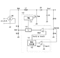
図2は、本発明の実施例による力率補正回路を示す図である。 FIG. 2 is a diagram illustrating a power factor correction circuit according to an embodiment of the present invention.
図2に示したように、本発明の実施例による力率補正回路は、ブリッジダイオード(BD)と、インダクタ(L1)、スイッチ(Qsw)、ダイオード(D1)及びキャパシタ(C1)で構成されたブースト回路と、スイッチング制御部100を含む。以下、特許請求の範囲に至るまで、便宜上、インダクタ(L1)、スイッチ(Qsw)、ダイオード(D1)及びキャパシタ(C1)を含んで構成される回路を”ブースト回路”と称する。この回路のスイッチ(Qsw)は、電流端子の一つが、回路の交流入力端から直流出力端に至る電流路に接続され、又、交流入力端から整流回路を経てブースト回路の直流入力端に至る電流路、分圧回路、掛け算回路、パルス幅変調回路(PWM)を経て、スイッチ(Qsw)の制御端子に情報が送られていて、交流入力端とスイッチが結合されている。
As shown in FIG. 2, the power factor correction circuit according to the embodiment of the present invention includes a bridge diode (BD), an inductor (L1), a switch (Qsw), a diode (D1), and a capacitor (C1). A boost circuit and a
ブリッジダイオード(BD)は、外部から入力される交流電圧(AC)を整流して全波整流電圧(Vbd)を出力する。スイッチング制御部100は、分圧センシングされた整流電圧の信号(Vbd’)及び分圧センシングされた出力電圧の信号(Vsense=Vout*R4/(R3+R4))を受信して、スイッチ(Qsw)の導通/遮断を制御する制御信号を生成し、スイッチング制御部100の制御信号によってスイッチ(Qsw)が導通/遮断されて、ブースト回路のキャパシタ(C1)に一定の直流電圧(Vout)が出力される。ここで、“導通/遮断”は“導通または遮断”を意味する。
The bridge diode (BD) rectifies an alternating voltage (AC) input from the outside and outputs a full-wave rectified voltage (Vbd). The
ここで、本発明の実施例による力率補正回路は、スイッチング制御部100で生成される基準電圧が入力電圧によって異なって設定され、これによって互いに異なる出力電圧(Vout)が出力されるが、入力電圧がいくらなのかを別途の回路を用いずに、センシングされた出力電圧(Vsense)を利用して感知するので、回路全体の製作経費を節減できる特徴がある。このための具体的方法は、以下に説明する。図2で”Vbd”は、ブリッジダイオード(BD)の出力電圧を意味し、これは入力される電圧である交流電圧(AC)の全波整流値である。
Here, in the power factor correction circuit according to the embodiment of the present invention, the reference voltage generated by the
また、本発明の実施例による力率補正回路は、整流出力電圧(Vbd)をセンシングする抵抗(R1、R2)、ブースト出力電圧(Vout)をセンシングする抵抗(R3、R4)を含む。抵抗(R1、R2)は、互いに直列に連結されて、ブリッジダイオード(BD)の出力と接地線の間に連結され、抵抗(R2)に印加される分配電圧(Vbd´)がスイッチング制御部100の乗算器140に入力される。抵抗(R3、R4)は互いに直列に連結されて、キャパシタ(C1)の一端と接地線の間に連結され、抵抗(R4)にかかるセンシングされた出力電圧(Vsense)がスイッチング制御部100の比較器(Amp2)に入力される。ここで、抵抗(R1、R2)によってセンシングされた、整流出力電圧(Vbd)は、スイッチング制御部100で基準電圧(Vref2またはVref3)を生成するために使用されるのではなく、入力電流が入力電圧を推定することに使用される基準電流を生成するのに使用される。
The power factor correction circuit according to the embodiment of the present invention includes resistors (R1, R2) for sensing the rectified output voltage (Vbd) and resistors (R3, R4) for sensing the boost output voltage (Vout). The resistors (R1, R2) are connected in series with each other, and are connected between the output of the bridge diode (BD) and the ground line, and the distribution voltage (Vbd ′) applied to the resistor (R2) is changed to the
ブースト回路において、インダクタ(L1)の一端は、ブリッジダイオード(BD)の正極出力に連結されて、他端はダイオード(D1)のアノードに連結される。ダイオード(D1)のカソードはキャパシタ(C1)の一端に連結され、キャパシタ(C1)の他端は接地線に連結される。スイッチ(Qsw)はNチャネル電界効果トランジスタであって、そのドレーン端子は、インダクタ(L1)とダイオード(D1)の接続点に連結され、ソース端子は接地線に連結されて、ゲート端子はスイッチング制御部100のPWM回路出力端子に連結される。
In the boost circuit, one end of the inductor (L1) is connected to the positive output of the bridge diode (BD), and the other end is connected to the anode of the diode (D1). The cathode of the diode (D1) is connected to one end of the capacitor (C1), and the other end of the capacitor (C1) is connected to the ground line. The switch (Qsw) is an N-channel field effect transistor, its drain terminal is connected to the connection point of the inductor (L1) and the diode (D1), the source terminal is connected to the ground line, and the gate terminal is switching control. The PWM circuit output terminal of the
ここで、一般的な方法では、スイッチ(Qsw)のソース端子と接地線の間にスイッチ(Qsw)を通って流れる電流を感知する感知抵抗(図示せず)が連結されて、感知された電流がスイッチング制御部100に入力されるが、図2では便宜上図示していない。図2でスイッチ(Qsw)をMOSFETとして示したが、本発明はこれに限定されることなく、バイポーラトランジスタなど、他のスイッチング素子を使用することができる。
Here, in a general method, a sensing resistor (not shown) that senses a current flowing through the switch (Qsw) is connected between the source terminal of the switch (Qsw) and the ground line to detect the sensed current. Is input to the switching
一方、本発明の実施例による力率補正回路のスイッチング制御部100は、PWM回路120、乗算器140、比較器(Amp1)、基準電圧発生器160を含む。
Meanwhile, the switching
基準電圧発生器160は、逆相端子(−)にセンシングされた出力電圧(Vsense)が入力され、正相端子(+)に基準電圧(Vref1)が入力されて、二つの入力を比較する比較器(Amp2)、この比較器(Amp2)出力を受信して比較器(Amp2)の出力に対応して基準電圧(Vref2またはVref3)を生成する電圧生成器162を含む。そして、出力電圧(Vsense)が基準電圧(Vref1)より大きい場合には、比較器(Amp2)は負(−)の電圧を出力し、出力電圧(Vsense)が基準電圧(Vref1)より小さい場合には、比較器(Amp2)は正(+)の電圧を出力する。
The
比較器(Amp2)から正(+)の電圧が出力される場合、電圧生成器162は基準電圧(Vref2)を出力し、比較器(Amp2)から負(−)の電圧が出力される場合、電圧生成器162は基準電圧(Vref3)を出力する。電圧生成器162の具体的回路及び動作説明は、当業者ならば知ることができるため、具体的説明は省略する。ここで、基準電圧(Vref2)は、基準電圧(Vref3)より低い電圧に設定する。
When a positive (+) voltage is output from the comparator (Amp2), the
一方、基準電圧発生器160は、力率補正回路にAC入力電圧が最初印加される時点(T1)からスイッチ(Qsw)がスイッチング動作する時点(T2)までの出力センシング電圧(Vsense)に対してだけ、基準電圧(Vref2またはVref3)を出力し、スイッチ(Qsw)がスイッチング動作をして直流電圧を出力する時点以後(T2以後)については、既に設定された基準電圧(Vref2またはVref3)を、そのまま出力する。
On the other hand, the
比較器(Amp1)の逆相端子(−)にはセンシングされた出力電圧(Vsense)が入力され、正相端子(+)には基準電圧発生器160から出力される基準電圧(Vref2またはVref3)が入力されて、両電圧を比較して対応する電圧を出力する。乗算器140は、抵抗(R1、R2)によってセンシングされた全波整流電圧の信号(Vbd´)に比較器(Amp1)の出力をかけてPWM回路120に出力する。この時、乗算器140の出力は、全波整流電圧と同一な形態を有し、PWM回路120で基準電流として使用される。PWM回路120は、乗算器140から出力される基準電流とスイッチ(Qsw)を通って流れる電流を比較して、スイッチ(Qsw)を導通/遮断するゲート信号を生成してスイッチ(Qsw)のゲート端子に出力する。
The sensed output voltage (Vsense) is input to the negative phase terminal (−) of the comparator (Amp1), and the reference voltage (Vref2 or Vref3) output from the
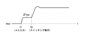
以下、図2及び図3を参照して本発明の実施例による力率補正回路の動作に対して説明する。図3は、交流入力が印加されて、力率補正回路が初期起動された後、出力電圧(Vout)の変化を示す図である。ここで、初期起動とは、所定時間の無入力の後に交流入力を印加して、入力交流電圧のピーク電圧を推測可能にする動作である。 Hereinafter, the operation of the power factor correction circuit according to the embodiment of the present invention will be described with reference to FIGS. FIG. 3 is a diagram illustrating a change in the output voltage (Vout) after an AC input is applied and the power factor correction circuit is initially activated. Here, the initial activation is an operation that makes it possible to estimate the peak voltage of the input AC voltage by applying an AC input after no input for a predetermined time.
図3の時点(T1)は、力率補正回路の入力交流電圧(AC)が印加される時点であり、時点(T2)は、継続してオフだったスイッチ(Qsw)がオン・オフ動作を始めて、キャパシタ(C1)の高電圧充電を始める時点である。入力交流電圧(AC)が印加された時点(T1)からスイッチ(Qsw)がスイッチングを始める時点まで、図3に示したように出力電圧(Vout)は、T1からT2までで入力交流電圧(AC)のピーク電圧(√2*Vac)になり、負荷電流が安定して、インダクタL1の電圧降下が零になる。つまり、時点(T1)から時点(T2)までは、スイッチ(Qsw)が動作する前であるため、整流された電圧(Vbd)は、インダクタ(L1)、ダイオード(D1)を通ってキャパシタ(C1)に充電され、そのためにキャパシタ(C1)には入力交流電圧(AC)のピーク電圧(√2*Vac)が充電される。また、スイッチ(Qsw)がスイッチング動作をした後に、出力電圧(Vout)は所望の直流出力電圧が出力される。 The time point (T1) in FIG. 3 is the time point when the input AC voltage (AC) of the power factor correction circuit is applied, and the time point (T2) is the time when the switch (Qsw) that has been continuously turned off performs the on / off operation. For the first time, the capacitor (C1) starts to be charged at high voltage. From the time when the input AC voltage (AC) is applied (T1) to the time when the switch (Qsw) starts switching, the output voltage (Vout) is changed from T1 to T2 as shown in FIG. ) Peak voltage (√2 * Vac), the load current is stabilized, and the voltage drop of the inductor L1 becomes zero. That is, since the time point (T1) to the time point (T2) is before the switch (Qsw) is operated, the rectified voltage (Vbd) passes through the inductor (L1) and the diode (D1), and the capacitor (C1 Therefore, the capacitor (C1) is charged with the peak voltage (√2 * Vac) of the input AC voltage (AC). Further, after the switch (Qsw) performs a switching operation, a desired DC output voltage is output as the output voltage (Vout).
従って、T1からT2までの出力電圧(Vout)は、入力交流電圧(AC)がどのような範囲の電圧が印加されるかを決定するための情報になるため、本発明の実施例による力率補正回路は、外部の他の回路を使用しなくても、このピーク電圧を利用して入力電圧の範囲を判断する。一方、図3に示したように、スイッチ(Qsw)がスイッチング動作を遂行した後、出力電圧が急激に変わることはなく、緩やかに変わるため、入力交流電圧(AC)の情報を示す出力電圧(Vout)として、時点(T2)より所定の時間後の時点で測定された電圧を利用することができる。 Therefore, since the output voltage (Vout) from T1 to T2 is information for determining what range of voltage is applied to the input AC voltage (AC), the power factor according to the embodiment of the present invention. The correction circuit determines the range of the input voltage using this peak voltage without using any other external circuit. On the other hand, as shown in FIG. 3, after the switch (Qsw) performs the switching operation, the output voltage does not change abruptly and changes slowly, so that the output voltage (AC) indicating the information of the input AC voltage (AC) As Vout), a voltage measured at a time point after a predetermined time from the time point (T2) can be used.
即ち、入力交流電圧(AC)が80Vac乃至150Vac範囲なのか、150Vac乃至256Vac範囲なのかをT1からT2時点までの出力電圧(Vout)によって判断することができて、それによって出力電圧(Vout)を設定することができる。ここで、”Vac”は入力交流電圧(AC)の実効値を示し、全波整流された電圧(Vbd)は入力交流電圧(AC)を全波整流した値であるため、全波整流電圧(Vbd)のピーク電圧も入力交流電圧(AC)のピーク電圧(*Vac)とほとんど同じ電圧である。 That is, whether the input AC voltage (AC) is in the range of 80 Vac to 150 Vac or 150 Vac to 256 Vac can be determined from the output voltage (Vout) from T1 to T2, and the output voltage (Vout) is thereby determined. Can be set. Here, “Vac” represents the effective value of the input AC voltage (AC), and the full-wave rectified voltage (Vbd) is a value obtained by full-wave rectification of the input AC voltage (AC). The peak voltage of Vbd) is almost the same voltage as the peak voltage (* Vac) of the input AC voltage (AC).
T1からT2時点までの出力電圧(Vout)、つまり入力交流電圧のピーク電圧(√2*Vac)は、抵抗(R3、R4)によってセンシングされ、センシングされた電圧(Vsense)は、比較器(Amp2)の逆相端子に入力される。以下、入力交流電圧(AC)が80Vac乃至150Vac範囲の場合にセンシングされた電圧(Vsense1)と、入力交流電圧(AC)が150Vac乃至250Vacの範囲の場合にセンシングされた電圧(Vsense2)に対して、各々出力電圧(Vout)が変化される方法に対して調べる。ここで、電圧(Vsense2)は電圧(Vsense1)より高電圧である。 The output voltage (Vout) from T1 to T2, that is, the peak voltage (√2 * Vac) of the input AC voltage is sensed by the resistors (R3, R4), and the sensed voltage (Vsense) is the comparator (Amp2). ). Hereinafter, with respect to the voltage (Vsense1) sensed when the input AC voltage (AC) is in the range of 80 Vac to 150 Vac and the voltage (Vsense2) sensed when the input AC voltage (AC) is in the range of 150 Vac to 250 Vac. In each case, the method in which the output voltage (Vout) is changed is examined. Here, the voltage (Vsense2) is higher than the voltage (Vsense1).
まず、センシングされた電圧がVsense1の場合、比較器(Amp2)は、基準電圧(Vref1)とVsense1を比較して正(+)電圧を出力する。ここで、基準電圧(Vref1)は、入力交流電圧(AC)が80Vac乃至150Vac範囲なのか150Vac乃至250Vac範囲なのかを判断する基準として使用され、これを判断するために予め設定された電圧である。比較器(Amp2)で正の電圧が出力される場合、電圧生成器162は低電圧であるVref2を生成して比較器(Amp1)に出力する。
First, when the sensed voltage is Vsense1, the comparator (Amp2) compares the reference voltage (Vref1) with Vsense1 and outputs a positive (+) voltage. Here, the reference voltage (Vref1) is used as a reference for determining whether the input AC voltage (AC) is in the range of 80 Vac to 150 Vac or 150 Vac to 250 Vac, and is a voltage set in advance to determine this. . When a positive voltage is output from the comparator (Amp2), the
ここで、基準電圧発生器160が時点(T1)から時点(T2)までに生成した基準電圧(Vref2)は、時点(T2)以後には固定される。基準電圧発生器160で生成された基準電圧(Vref2)は、比較器(Amp1)の正相端子(+)に入力されて、比較器(Amp1)は、センシングされた電圧(Vsense)と基準電圧(Vref2)を比較して対応値を出力する。ここで、乗算器140は、比較器(Amp1)の出力と電圧(Vbd´)をかけてPWM回路120に基準電流を提供し、PWM回路120は、この基準電流を利用してスイッチ(Qsw)を導通または遮断にするよう制御する。PWM回路120の導通/遮断制御信号によってスイッチ(Qsw)が導通/遮断されて、入力電流が入力電圧に追従し、出力電圧が基準電圧(Vref2)に対応して直流電圧Vout1を出力する。従って、入力交流電圧が(AC)80Vac乃至150Vac範囲である場合、これに対応する出力電圧であるVout1を出力する。
Here, the reference voltage (Vref2) generated from the time point (T1) to the time point (T2) by the
次に、センシングされた電圧がVsense2の場合、比較器(Amp2)は基準電圧(Vref1)とVsense2を比較して、負(−)電圧を出力する。この時、比較器(Amp2)に負(−)電圧が出力される場合、電圧生成器162は、Vref2より高電圧であるVref3を生成して、比較器(Amp1)の正相端子(+)に出力する。ここで、図3に示したように、時点(T2)以後または時点(T2)以後の所定の時間後には、センシングされた電圧(Vesene)が交流入力電圧(AC)の範囲の情報を示さないので、基準電圧発生器160が時点(T1)から時点(T2)までに生成した基準電圧(Vref3)は、時点(T2)以後には固定される。基準電圧発生器160で生成された基準電圧(Vref3)は、比較器(Amp1)の正相端子(+)に入力されて、比較器(Amp1)はセンシングされた電圧(Vsense)と基準電圧(Vref3)を比較して、対応値を出力する。ここで、乗算器140は、比較器(Amp1)の出力と電圧(Vbd´)をかけてPWM回路120に基準電流を提供し、PWM回路120は、この基準電流を利用してスイッチ(Qsw)の導通/遮断を制御する。PWM回路120の導通/遮断制御信号によって、スイッチ(Qsw)が導通/遮断されて入力電流が入力電圧に追従し、出力電圧(Vout)が基準電圧(Vref3)に対応してVout1電圧より高い直流電圧Vout2を出力する。従って、入力交流電圧(AC)が150Vac乃至250Vac範囲である場合、これに対応する出力電圧であるVout2を出力する。
Next, when the sensed voltage is Vsense2, the comparator (Amp2) compares the reference voltage (Vref1) with Vsense2, and outputs a negative (-) voltage. At this time, when a negative (−) voltage is output to the comparator (Amp2), the
このように本発明は、外部から入力交流電圧(AC)が入力される場合、所定の時点まで(例えば、T2時点まで)センシングされた出力電圧(Vsense)は、入力交流電圧(AC)の情報を有している点を利用して、基準電圧(Vref2またはVref3)を生成することによって、別途の追加装置を要せず、入力交流電圧(AC)に対応して出力電圧(Vout)を生成することができる。また、入力交流電圧(AC)に対応して出力電圧(Vout)を生成するため、電力損失も減らすことができる。 As described above, according to the present invention, when the input AC voltage (AC) is input from the outside, the output voltage (Vsense) sensed until a predetermined time (for example, until the time T2) is the information on the input AC voltage (AC). By generating the reference voltage (Vref2 or Vref3) by using the point having the output voltage, the output voltage (Vout) is generated corresponding to the input AC voltage (AC) without the need for a separate additional device. can do. Moreover, since the output voltage (Vout) is generated corresponding to the input AC voltage (AC), the power loss can be reduced.
一方、本発明の実施例では、整流された交流電圧(Vbd)をセンシングする力率補正回路について説明したが、本発明は、整流された交流電圧(Vbd)をセンシングしない力率補正回路にも適用することができる。つまり、本発明は、入力電流が入力電圧の形態で追従するように制御される全ての力率補正回路に適用できる。 On the other hand, in the embodiment of the present invention, the power factor correction circuit that senses the rectified AC voltage (Vbd) has been described. However, the present invention also applies to a power factor correction circuit that does not sense the rectified AC voltage (Vbd). Can be applied. That is, the present invention can be applied to all power factor correction circuits that are controlled so that the input current follows the form of the input voltage.
図4は、他の実施例による力率補正回路を示す図である。つまり、図4は整流された交流電圧をセンシングしない力率補正回路を示す図である。 FIG. 4 is a diagram showing a power factor correction circuit according to another embodiment. That is, FIG. 4 is a diagram illustrating a power factor correction circuit that does not sense a rectified AC voltage.
図4に示された力率補正回路は、全波整流された交流電圧をセンシングしないため、乗算器140が除去されたこと以外には、図2の力率補正回路構成及び動作はほとんど類似している。つまり、入力交流電圧(AC)が80Vac乃至150Vac範囲なのか、150Vac乃至256Vac範囲なのかをT1からT2時点までの出力電圧(Vout)を通じて判断し、判断された入力交流電圧によって、基準電圧発生器160は二つの基準電圧(Vref2、Vref3)のうち、一つの基準電圧を出力する。また、PWM回路120は、整流された交流電圧を受信しないで、比較器(Amp1)の出力のみを通じてスイッチ(Qsw)のスイッチングを制御する。
Since the power factor correction circuit shown in FIG. 4 does not sense a full-wave rectified AC voltage, the configuration and operation of the power factor correction circuit in FIG. 2 are almost similar except that the
以上で本発明の好ましい実施例について詳細に説明したが、本発明の権利範囲はこれに限定されることはなく、請求範囲で定義している本発明の基本概念を利用した当業者のいろいろな変形及び改良形態も本発明の権利範囲に属する。 The preferred embodiments of the present invention have been described in detail above. However, the scope of the present invention is not limited to this, and various skilled in the art using the basic concept of the present invention defined in the claims. Variations and improvements are also within the scope of the present invention.
100 スイッチング制御部
120 PWM回路
140 乗算器
160 基準電圧発生器
162 電圧生成器
100
Claims (6)
前記入力端に結合したスイッチの動作によって出力端に前記昇圧された直流出力電圧を供給するブースト回路と、
前記ブースト回路の入力端に交流入力電圧が入力された時点(T1)から、前記ブースト回路の前記スイッチがオンオフ動作を開始する時点(T2)までの所定の期間で、前記交流入力電圧のピーク値に等しい前記ブースト回路の出力端から出力された直流出力電圧に応じて前記ブースト回路により前記昇圧された直流出力電圧を設定するための目標値となる複数の基準電圧(Vref2及びVref3)の何れか一を発生する基準電圧発生器を有してなり、前記基準電圧発生器にて前記発生された前記複数の基準電圧のうちの何れか一の基準電圧(Vref2又はVref3)に基づいて前記スイッチの動作を制御するスイッチング制御部とを備え、
前記スイッチング制御部は、前記基準電圧発生器から出力される前記何れか一の基準電圧(Vref2又はVref3)と前記ブースト回路の出力端に出力される前記直流出力電圧を比較する第1比較器と、前記第1比較器の出力に基づいて前記スイッチの動作を制御するPWM回路と、
さらに前記基準電圧発生器の内部に、前記所定の期間で、前記ブースト回路の出力端から出力される前記直流出力電圧と、前記交流入力電圧が第1電圧範囲に属するか或いは前記第1電圧範囲より高い第2電圧範囲に属するかを識別するための所定の基準電圧(Vref1)を比較する第2比較器と、前記第2比較器の出力によって前記第1基準電圧(Vref2)または第2基準電圧(Vref3)を発生する電圧発生器と
を備えることを特徴とする力率補正回路。 In the power factor correction circuit that converts the AC input voltage supplied to the input terminal into a boosted DC output voltage and corrects the power factor,
A boost circuit for supplying the boosted DC output voltage to an output terminal by an operation of a switch coupled to the input terminal;
The peak value of the AC input voltage during a predetermined period from the time (T1) when the AC input voltage is input to the input terminal of the boost circuit to the time (T2) when the switch of the boost circuit starts ON / OFF operation. Any one of a plurality of reference voltages (Vref2 and Vref3) serving as target values for setting the DC output voltage boosted by the boost circuit according to the DC output voltage output from the output terminal of the boost circuit equal to And a reference voltage generator for generating one of the switches based on any one of the plurality of reference voltages (Vref2 or Vref3) generated by the reference voltage generator. A switching control unit for controlling the operation,
The switching control unit includes a first comparator that compares the any one reference voltage (Vref2 or Vref3) output from the reference voltage generator with the DC output voltage output to the output terminal of the boost circuit. A PWM circuit for controlling the operation of the switch based on the output of the first comparator;
Further, the DC output voltage output from the output terminal of the boost circuit and the AC input voltage within the reference voltage generator within the predetermined period belong to the first voltage range or the first voltage range. A second comparator for comparing a predetermined reference voltage (Vref1) for identifying whether it belongs to a higher second voltage range, and the first reference voltage (Vref2) or the second reference depending on the output of the second comparator A voltage generator for generating a voltage (Vref3);
Power factor correction circuit, characterized in that it comprises a.
前記PWM回路は前記乗算器からの乗算出力に基づいて前記スイッチの動作を制御することを特徴とする請求項2記載の力率補正回路。 3. The power factor correction circuit according to claim 2, wherein the PWM circuit controls the operation of the switch based on a multiplication output from the multiplier.
前記ブースト回路の出力端と接地線の間に互いに直列に連結される第3抵抗及び第4抵抗をさらに備え、
前記第1抵抗と前記第2抵抗の接続点の電圧が前記乗算器に入力され、前記第3抵抗と前記第4抵抗の接続点の電圧が前記第1比較器及び第2比較器に入力されることを特徴とする請求項3に記載の力率補正回路。 A first resistor and a second resistor connected in series between the input terminal of the boost circuit and a ground line;
A third resistor and a fourth resistor connected in series between the output terminal of the boost circuit and the ground line;
The voltage at the connection point between the first resistor and the second resistor is input to the multiplier, and the voltage at the connection point between the third resistor and the fourth resistor is input to the first comparator and the second comparator. The power factor correction circuit according to claim 3.
前記力率補正回路は、前記入力端に結合したスイッチの動作によって出力端に前記昇圧された直流出力電圧を供給するブースト回路と、前記ブースト回路の入力端に交流入力電圧が入力された時点(T1)から、前記ブースト回路の前記スイッチがオンオフ動作を開始する時点(T2)までの所定の期間で、前記交流入力電圧のピーク値に等しい前記ブースト回路の出力端から出力された直流出力電圧に応じて前記ブースト回路により前記昇圧された直流出力電圧を設定するための目標値となる複数の基準電圧(Vref2及びVref3)の何れか一を発生する基準電圧発生器を有してなり、前記基準電圧発生器にて前記生成された前記複数の基準電圧のうちの何れか一の基準電圧(Vref2又はVref3)に基づいて前記スイッチの動作を制御するスイッチング制御部とを備えており、
前記方法は、前記スイッチング制御部によって処理される、
前記所定の期間で、前記ブースト回路の出力端から出力される前記直流出力電圧と、前記交流入力電圧が第1電圧範囲に属するか或いは前記第1電圧範囲より高い第2電圧範囲に属するかを識別するための所定の基準電圧(Vref1)を比較する一方の比較段階と、
前記比較の段階の出力によって第1基準電圧(Vref2)または第2基準電圧(Vref3)を生成する基準電圧発生段階と、
前記基準電圧発生段階が出力した基準電圧と前記ブースト回路の出力端に出力される前記直流出力電圧を比較する他方の比較段階と、
前記他方の比較段階の出力に基づいて前記スイッチの動作をPWM回路を用いて制御するスイッチ動作制御段階と
を備えることを特徴とする力率補正回路の出力電圧制御方法。 In the method of controlling the output voltage of the power factor correction circuit for correcting the power factor while converting the AC input voltage supplied to the input terminal into a boosted DC output voltage,
The power factor correction circuit includes a boost circuit that supplies the boosted DC output voltage to an output terminal by an operation of a switch coupled to the input terminal, and a time point when an AC input voltage is input to the input terminal of the boost circuit ( The DC output voltage output from the output terminal of the boost circuit is equal to the peak value of the AC input voltage during a predetermined period from T1) to the time point (T2) when the switch of the boost circuit starts an on / off operation. And a reference voltage generator for generating any one of a plurality of reference voltages (Vref2 and Vref3) serving as a target value for setting the DC output voltage boosted by the boost circuit. Based on one reference voltage (Vref2 or Vref3) of the plurality of reference voltages generated by the voltage generator, the switch And a switching control unit for controlling the work,
The method is processed by the switching controller.
Whether the DC output voltage output from the output terminal of the boost circuit and the AC input voltage belong to a first voltage range or a second voltage range higher than the first voltage range in the predetermined period. One comparison stage for comparing a predetermined reference voltage (Vref1) for identification;
A reference voltage generation step of generating a first reference voltage (Vref2) or a second reference voltage (Vref3) according to the output of the comparison step;
The other comparison step of comparing the reference voltage output from the reference voltage generation step and the DC output voltage output to the output terminal of the boost circuit;
A switch operation control step of controlling the operation of the switch using a PWM circuit based on the output of the other comparison step;
Output voltage control method of the power factor correction circuit, characterized in that it comprises a.
前記一方の比較段階の前記比較出力が前記所定の期間で前記ブースト回路の出力端に出力される前記直流出力電圧が前記第1電圧範囲に属することを示すと前記第1基準電圧を生成し、
或いは、前記一方の比較段階の前記比較出力が前記所定の期間で前記ブースト回路の出力端に出力される前記直流出力電圧が前記第2電圧範囲に属することを示すと前記第1基準電圧より高い前記第2基準電圧を生成する
ことを特徴とする請求項5記載の力率補正回路の出力電圧制御方法。 The reference voltage generation step includes:
When the comparison output of the one comparison stage indicates that the DC output voltage output to the output terminal of the boost circuit in the predetermined period belongs to the first voltage range, the first reference voltage is generated,
Alternatively, if the comparison output of the one comparison stage indicates that the DC output voltage output to the output terminal of the boost circuit in the predetermined period belongs to the second voltage range, it is higher than the first reference voltage. Generating the second reference voltage
6. The output voltage control method for a power factor correction circuit according to claim 5, wherein:
Applications Claiming Priority (1)
| Application Number | Priority Date | Filing Date | Title |
|---|---|---|---|
| KR1020040075537A KR101058936B1 (en) | 2004-09-21 | 2004-09-21 | Power factor correction circuit and its output voltage control method |
Publications (2)
| Publication Number | Publication Date |
|---|---|
| JP2006094696A JP2006094696A (en) | 2006-04-06 |
| JP4637694B2 true JP4637694B2 (en) | 2011-02-23 |
Family
ID=36073773
Family Applications (1)
| Application Number | Title | Priority Date | Filing Date |
|---|---|---|---|
| JP2005262523A Expired - Fee Related JP4637694B2 (en) | 2004-09-21 | 2005-09-09 | Power factor correction circuit and output voltage control method thereof |
Country Status (6)
| Country | Link |
|---|---|
| US (1) | US7501800B2 (en) |
| JP (1) | JP4637694B2 (en) |
| KR (1) | KR101058936B1 (en) |
| CN (1) | CN1753291B (en) |
| DE (1) | DE102005044325A1 (en) |
| TW (1) | TWI321272B (en) |
Families Citing this family (21)
| Publication number | Priority date | Publication date | Assignee | Title |
|---|---|---|---|---|
| GB0326070D0 (en) * | 2003-11-07 | 2003-12-10 | Newage Int Ltd | An AC power generating system |
| TW200826444A (en) * | 2006-07-27 | 2008-06-16 | Koninkl Philips Electronics Nv | Switch mode power supply for in-line voltage applications |
| CN101282079B (en) * | 2007-04-05 | 2011-06-01 | 昂宝电子(上海)有限公司 | System and method for power controller |
| US7843184B2 (en) * | 2007-12-31 | 2010-11-30 | Intel Corporation | Power supply with separate line regulation and load regulation |
| US7888917B2 (en) * | 2008-04-23 | 2011-02-15 | Honeywell International Inc. | Systems and methods for producing a substantially constant output voltage in a power source boost system |
| US8674544B2 (en) * | 2009-01-26 | 2014-03-18 | Geneva Cleantech, Inc. | Methods and apparatus for power factor correction and reduction of distortion in and noise in a power supply delivery network |
| WO2010085817A1 (en) * | 2009-01-26 | 2010-07-29 | Geneva Cleantech Inc. | Methods and apparatus for power factor correction and reduction of distortion in and noise in a power supply delivery network |
| US8098503B2 (en) | 2010-02-09 | 2012-01-17 | Power Integrations, Inc. | Method and apparatus to control a power converter having a low loop bandwidth |
| KR101948128B1 (en) * | 2010-02-17 | 2019-02-15 | 페어차일드코리아반도체 주식회사 | Control device,led emitting light device comprising the same, and control method |
| KR101097267B1 (en) * | 2010-03-02 | 2011-12-22 | 삼성에스디아이 주식회사 | Energy storage system and controlling method of the same |
| GB201107171D0 (en) * | 2011-04-28 | 2011-06-15 | Tridonic Gmbh & Co Kg | Power factor correction |
| US20130057229A1 (en) * | 2011-09-02 | 2013-03-07 | Intersil Americas Inc. | Power factor correction apparatus and method |
| KR101984927B1 (en) * | 2011-12-29 | 2019-06-04 | 서울반도체 주식회사 | Led driving circuit and luminescence apparatus comprising the same |
| KR101507139B1 (en) * | 2013-04-24 | 2015-03-31 | (주)실리콘인사이드 | Boost converter improved line regulation |
| CN103390995B (en) * | 2013-07-18 | 2015-09-30 | 矽力杰半导体技术(杭州)有限公司 | A kind of pfc circuit |
| CN104079169A (en) * | 2014-06-24 | 2014-10-01 | 华为技术有限公司 | Circuit of switching inductance power supply |
| CN105425889B (en) * | 2015-11-09 | 2017-07-04 | 华北电力大学(保定) | A kind of high precision voltage stabilization and current stabilization control circuit based on the pre- steady level of high frequency electric source |
| CN107342678A (en) * | 2017-08-29 | 2017-11-10 | 成都雷电微力科技有限公司 | A kind of Switching Power Supply output overshoot suppression circuit and Switching Power Supply |
| TWI641225B (en) * | 2018-05-03 | 2018-11-11 | 廣達電腦股份有限公司 | Voltage band-pass enable circuit |
| TWI786875B (en) * | 2021-10-08 | 2022-12-11 | 海韻電子工業股份有限公司 | Control Module of Power Correction Circuit |
| CN115940626B (en) * | 2023-02-08 | 2023-05-23 | 合肥联宝信息技术有限公司 | Power supply control circuit, power supply control method, electronic equipment and storage medium |
Family Cites Families (10)
| Publication number | Priority date | Publication date | Assignee | Title |
|---|---|---|---|---|
| US5003454A (en) * | 1990-01-09 | 1991-03-26 | North American Philips Corporation | Power supply with improved power factor correction |
| US5289361A (en) | 1991-01-16 | 1994-02-22 | Vlt Corporation | Adaptive boost switching preregulator and method |
| US5594323A (en) * | 1991-02-21 | 1997-01-14 | Siemens Aktiengesellschaft | Control process for a voltage transformer with a wide input voltage range and the application of such a process |
| GB9104070D0 (en) * | 1991-02-27 | 1991-04-17 | Astec Int Ltd | Power supplies |
| US5359276A (en) | 1993-05-12 | 1994-10-25 | Unitrode Corporation | Automatic gain selection for high power factor |
| KR100333973B1 (en) | 1999-06-14 | 2002-04-24 | 김덕중 | Power Factor Compensation Controller |
| JP3381254B2 (en) | 2000-03-16 | 2003-02-24 | サンケン電気株式会社 | AC-DC converter |
| JP4651861B2 (en) | 2001-06-14 | 2011-03-16 | 京セラ株式会社 | Step-up DC-DC converter and portable terminal using the same |
| CN100490284C (en) * | 2002-01-08 | 2009-05-20 | 三垦电气株式会社 | Power factor improving converter and control method thereof |
| US6686725B1 (en) | 2002-11-12 | 2004-02-03 | Samsung Electro-Mechanics Co., Ltd. | Power supply circuit compensating power factor |
-
2004
- 2004-09-21 KR KR1020040075537A patent/KR101058936B1/en active IP Right Grant
-
2005
- 2005-09-09 JP JP2005262523A patent/JP4637694B2/en not_active Expired - Fee Related
- 2005-09-16 TW TW094131983A patent/TWI321272B/en not_active IP Right Cessation
- 2005-09-16 DE DE102005044325A patent/DE102005044325A1/en not_active Withdrawn
- 2005-09-21 US US11/232,737 patent/US7501800B2/en active Active
- 2005-09-21 CN CN200510109733XA patent/CN1753291B/en active Active
Also Published As
| Publication number | Publication date |
|---|---|
| KR101058936B1 (en) | 2011-08-23 |
| US20060062031A1 (en) | 2006-03-23 |
| TW200611098A (en) | 2006-04-01 |
| JP2006094696A (en) | 2006-04-06 |
| TWI321272B (en) | 2010-03-01 |
| US7501800B2 (en) | 2009-03-10 |
| CN1753291A (en) | 2006-03-29 |
| DE102005044325A1 (en) | 2006-03-23 |
| CN1753291B (en) | 2010-10-13 |
| KR20060026700A (en) | 2006-03-24 |
Similar Documents
| Publication | Publication Date | Title |
|---|---|---|
| JP4637694B2 (en) | Power factor correction circuit and output voltage control method thereof | |
| KR101026248B1 (en) | Power Factor Correction Circuit | |
| US9866134B2 (en) | Control circuits and methods for regulating output voltages using multiple and/or adjustable reference voltages | |
| US20120155123A1 (en) | Reverse shunt regulator | |
| US8363428B2 (en) | Adapter power supply having variable switching mode | |
| KR100758127B1 (en) | Power supply unit | |
| WO2009025517A2 (en) | Power factor correction circuit | |
| US20060055386A1 (en) | Power factor improving circuit and control circuit for power factor improving circuit | |
| US10498257B2 (en) | Switching power converters controlled with control signals having variable on-times | |
| JP2007068319A (en) | Output voltage detection circuit, insulated switching power supply, and semiconductor device | |
| JP2009153234A (en) | Switching power supply device | |
| JP2010226807A (en) | Dc power supply apparatus | |
| US11404956B2 (en) | Power conversion apparatus and AC-DC conversion apparatus | |
| JP5222587B2 (en) | Power factor correction circuit | |
| JP2012039736A (en) | Power supply device | |
| KR102219639B1 (en) | Clamping circuit, power supply device comprising the same, and driving method of power supply device | |
| JP2001145347A (en) | Switching power supply | |
| KR102372846B1 (en) | Control circuit of power factor correction converter operating in critical conduction mode and power factor correction converter comprising thtereof | |
| US8619440B2 (en) | Over current protection method used in a switched-mode power supply and related controller | |
| JP6447593B2 (en) | Switching power supply device and semiconductor device | |
| JP2003348848A (en) | Power factor improving circuit | |
| JP2005168146A (en) | Switching power supply device | |
| JP2011234518A (en) | Switching power supply unit | |
| JP2003143845A (en) | High-voltage power source | |
| JP2000116124A (en) | Power circuit |
Legal Events
| Date | Code | Title | Description |
|---|---|---|---|
| A131 | Notification of reasons for refusal |
Free format text: JAPANESE INTERMEDIATE CODE: A131 Effective date: 20080129 |
|
| A601 | Written request for extension of time |
Free format text: JAPANESE INTERMEDIATE CODE: A601 Effective date: 20080430 |
|
| A602 | Written permission of extension of time |
Free format text: JAPANESE INTERMEDIATE CODE: A602 Effective date: 20080507 |
|
| A521 | Request for written amendment filed |
Free format text: JAPANESE INTERMEDIATE CODE: A523 Effective date: 20080522 |
|
| A02 | Decision of refusal |
Free format text: JAPANESE INTERMEDIATE CODE: A02 Effective date: 20080805 |
|
| A521 | Request for written amendment filed |
Free format text: JAPANESE INTERMEDIATE CODE: A523 Effective date: 20081030 |
|
| A911 | Transfer to examiner for re-examination before appeal (zenchi) |
Free format text: JAPANESE INTERMEDIATE CODE: A911 Effective date: 20081217 |
|
| A912 | Re-examination (zenchi) completed and case transferred to appeal board |
Free format text: JAPANESE INTERMEDIATE CODE: A912 Effective date: 20090227 |
|
| A601 | Written request for extension of time |
Free format text: JAPANESE INTERMEDIATE CODE: A601 Effective date: 20100922 |
|
| A602 | Written permission of extension of time |
Free format text: JAPANESE INTERMEDIATE CODE: A602 Effective date: 20100928 |
|
| A521 | Request for written amendment filed |
Free format text: JAPANESE INTERMEDIATE CODE: A523 Effective date: 20101005 |
|
| A01 | Written decision to grant a patent or to grant a registration (utility model) |
Free format text: JAPANESE INTERMEDIATE CODE: A01 |
|
| A61 | First payment of annual fees (during grant procedure) |
Free format text: JAPANESE INTERMEDIATE CODE: A61 Effective date: 20101124 |
|
| FPAY | Renewal fee payment (event date is renewal date of database) |
Free format text: PAYMENT UNTIL: 20131203 Year of fee payment: 3 |
|
| R150 | Certificate of patent or registration of utility model |
Free format text: JAPANESE INTERMEDIATE CODE: R150 |
|
| R250 | Receipt of annual fees |
Free format text: JAPANESE INTERMEDIATE CODE: R250 |
|
| R250 | Receipt of annual fees |
Free format text: JAPANESE INTERMEDIATE CODE: R250 |
|
| LAPS | Cancellation because of no payment of annual fees |