JP4636635B2 - Disc playback apparatus and disc playback method - Google Patents
Disc playback apparatus and disc playback method Download PDFInfo
- Publication number
- JP4636635B2 JP4636635B2 JP06660497A JP6660497A JP4636635B2 JP 4636635 B2 JP4636635 B2 JP 4636635B2 JP 06660497 A JP06660497 A JP 06660497A JP 6660497 A JP6660497 A JP 6660497A JP 4636635 B2 JP4636635 B2 JP 4636635B2
- Authority
- JP
- Japan
- Prior art keywords
- data
- detection
- sector
- signal
- identification address
- Prior art date
- Legal status (The legal status is an assumption and is not a legal conclusion. Google has not performed a legal analysis and makes no representation as to the accuracy of the status listed.)
- Expired - Fee Related
Links
Images


Classifications
-
- G—PHYSICS
- G11—INFORMATION STORAGE
- G11B—INFORMATION STORAGE BASED ON RELATIVE MOVEMENT BETWEEN RECORD CARRIER AND TRANSDUCER
- G11B20/00—Signal processing not specific to the method of recording or reproducing; Circuits therefor
- G11B20/10—Digital recording or reproducing
- G11B20/18—Error detection or correction; Testing, e.g. of drop-outs
- G11B20/1833—Error detection or correction; Testing, e.g. of drop-outs by adding special lists or symbols to the coded information
-
- G—PHYSICS
- G11—INFORMATION STORAGE
- G11B—INFORMATION STORAGE BASED ON RELATIVE MOVEMENT BETWEEN RECORD CARRIER AND TRANSDUCER
- G11B20/00—Signal processing not specific to the method of recording or reproducing; Circuits therefor
- G11B20/10—Digital recording or reproducing
Landscapes
- Engineering & Computer Science (AREA)
- Signal Processing (AREA)
- Rotational Drive Of Disk (AREA)
- Signal Processing For Digital Recording And Reproducing (AREA)
Description
【0001】
【発明の属する技術分野】
本発明は、デジタル信号を記録した光ディスクの再生装置および再生方法に関わる。
【0002】
【従来の技術】
ディスクを使用する再生装置としては、コンパクト・ディスク(CD)がある。
CD等ディスク状の記録媒体は一般に、記録密度を高めるため線速度一定方式(CLV)で記録されている。CLV方式で記録されている媒体は、回転数が内周と外周では、約2.6倍の差があり、再生中はデータを読み込むピックアップの移動にしたがって、媒体の回転数も変動する。そのため、アクセスの際には、ディスクの回転数は最大で約2.6倍変化するため規定の線速度となるまでデータの再生は出来なかった。これに対し、特開平5−250804号公報は、CLVで記録してあるディスクを回転数一定(CAV)で制御し、ピックアップ位置に従ってマスタクロックを変化させる。しかしこの方法では、モータを回転数一定で操作するために回転数検出手段を設けることが必要になり、構成が複雑になった。そこで、特開平6−89506号のように通常再生時は線速度一定で制御し、アクセス時のみ回転数一定で制御する方法が考案された。この方法では、現在のピックアップ位置と、アクセス後のピックアップ位置より、ディスク回転数や、クロック周波数を演算し、その結果に従ってクロックを発生させる必要があった。これは計算量を増大させ、アクセス中に計算が終了しない場合もあるという欠点があった。そこで、PLLを用いてディスクの回転に同期した再生クロックで、復調・誤り訂正を行う手段がとられた。この方法では、入力されたデータより、データに同期したクロックを再生し、そのクロックにより復調・誤り訂正を行う。そのため、アクセス時にも、スムーズな復調が可能になった。
【0003】
【発明が解決しようとする課題】
上記の方法では、ディスク上の傷などにより、データの読み出しができないと、クロックの再生が不安定となり、復調が不安定になると同時に、誤り訂正処理の信頼度が低下するという問題点がある。
【0004】
【課題を解決する為の手段】
本発明では、復調は、入力されたデータの入力レートに合わせて生成された再生クロックで行うのに対し、誤り訂正は、固定の周波数のクロックで動作させる。ブロックの先頭を検出した時に発生される信号によりインクリメントするカウンタと、ブロック単位のデータを誤り訂正した時に発生される信号によりインクリメントするカウンタを設け、その値を比較し、その結果に基づいて、誤り訂正を開始する信号を発生する手段を設ける。誤り訂正は、固定時間で行い、再生速度を2倍、4倍、j(j:自然数)倍と切り替えても同一とする。
【0005】
【発明の実施の形態】
本発明によるディスク再生装置の実施例を図面を用いて説明する。
【0006】
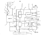
図1は、ディスク再生装置のブロック図である。なお、本実施例の説明では、図5、及び、図6に示されるフォーマットに従ったデータが入力される場合を前提にする。
【0007】
入力データのフォーマットについて説明する。図5において、時系列的に入力されたデータを、2048バイト単位に分割し、12バイトの付加データを主データの前に、4バイトの付加データを主データの後ろに書き加えた後、そのデータを172バイト単位に分割し、列とし、各列を、1列ずつ12列順にならべて、1セクタを構成する。連続する16個のセクタを順に並べて、1ブロックを構成する。図6において、POは、付加データ及び、主データに付加された列方向の誤り訂正符号であり、PIは、付加データ、主データ及び、POに付加された行方向の誤り訂正符号である。
【0008】
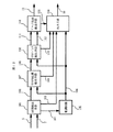
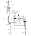
以下、図1について説明する。図1のディスク再生装置において、1はディスクであり、図6のフォーマットに従ったデータが変調されて記録された媒体である。2はディスク1を回転させるモータであり、3はディスク1に記録されているデータを読み取るピックアップであり、4はピックアップ3にディスク1より読み出されたシリアルデータである。5はシリアルデータ4から同期したクロックを作り出すPLLであり、入力データのビットレートに従ってクロック周波数は変化する。6はPLL5によって再生されたクロックであり、7はシリアルデータである。8はシリアルデータ7のブロックの先頭を検出し、復調する手段であり、その検出方法は、図7で説明する。9はモータの回転速度をコントロールする信号であり、10は復調されたデータであり、11は1ブロック分の信号の先頭を検出した信号である。12は入力されたデータを一時的に貯えておくRAMであり、13はデータの出力手段である。14は出力手段13の同期クロックであり、15は外部からデータを求める信号であり、16は出力手段13と外部とのデータバスである。17は誤り訂正を行う手段であり、18は誤り訂正手段17が発生する誤り訂正終了信号であり、19はブロック先頭検出信号をカウントする手段であり、復調カウンタと呼ぶ。20は誤り訂正終了信号をカウントする手段であり、誤り訂正カウンタと呼ぶ。21は復調カウンタ19と誤り訂正カウンタ20のカウンタ値を比較し、17に対して誤り訂正の開始信号22発生する手段である。23は誤り訂正手段17とRAM12間のデータバスを示し、24は出力手段13とRAM12間のデータバスである。25はこのシステム全体を統括するマイコンであり、26は25から発生されたアクセス信号である。27はクリスタルからマスタクロックを生成する水晶発振器である
動作クロックについて説明する。本ディスク再生装置は、2系統のクロックを持つ。再生クロックと、水晶クロックである。再生クロックは、PLL5によって、入力されたデータから再生される。ディスク1、モータ2、ピックアップ3、PLL5、復調手段8は、再生クロックで動作し、RAM12、出力手段13、誤り訂正手段17、復調カウンタ19、誤り訂正カウンタ20、比較手段21は水晶クロックで動作する。そのため、ディスク1、モータ2、ピックアップ3、PLL5、復調手段8はピックアップ3が取り込むデータの速さによって、クロック周波数は変化するが、 RAM12、出力手段13、誤り訂正手段17、復調カウンタ19、誤り訂正カウンタ20、比較手段21は常に固定周波数で動作する。
【0009】
ディスクは記録密度を高めるために、線速度一定(CLV)で記録されている。そのため、アクセス時など、ディスクの回転数が変わると、アクセス終了後、回転数が初期値に一致するまでは、入力レートは一時的に高くなったり、低くなったりし、再生クロックも変動する。そのため予め、再生クロックの周波数が±50%まで変動しても、復調できるようにしておく。1ブロック分のデータの誤り訂正は、n(n:自然数)倍速の1ブロック分のデータの復調より速く終了するように設定しておくと、誤り訂正は水晶発振のクロックで動作するため、復調の周波数変動の影響を受けずに独立して、かつ、復調よりも速く誤り訂正を行うことができる。
【0010】
以下、図1に示されるディスク再生装置の動作を入力より、順次説明する。
【0011】
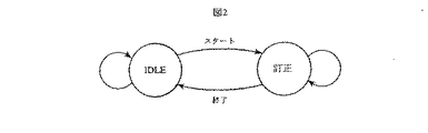
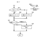
ピックアップ3は、ディスク1よりデータを読みだし、PLL5は、そのデータに同期してクロックを生成する。復調手段8は、ディスクより読みだされたシリアルデータを復調し、復調後のデータを逐次RAM12に転送する。又、復調手段8は、データのブロックの先頭を検出すると、復調カウンタ19へ先頭検出信号を送る。復調カウンタ19は、先頭検出信号を検出すると、カウンタをインクリメントする。RAM12は誤り訂正前のデータと、誤り訂正後のデータを記憶する。RAM12の内部のデータの配置については、図4で説明する。図2は、誤り訂正の状態遷移を示した図である。誤り訂正を行っていない時は、誤り訂正手段は信号入力待ちの状態を維持し続ける。これをアイドル状態と呼ぶ。アイドル状態の時に、比較手段より発生された誤り訂正開始信号が入力されると、RAM12の復調データを読みだし、誤り訂正を開始する。誤り訂正中は外部からの信号を受け付けず、一度誤り訂正が始まると、誤り訂正が終わり、その結果を再びRAM12に書き込み終わるまで、誤り訂正を続ける。誤り訂正中は、途中で処理が中断されることはない。誤り訂正が終わると、再びアイドル状態に戻る。誤り訂正が終了すると、誤り訂正終了信号を発生する。誤り訂正カウンタ20では誤り訂正終了信号を検出すると、カウンタをインクリメントする。比較手段21は2つの値の差が1以上になると、誤り訂正開始信号を出す。出力手段13は、誤り訂正したデータを出力する。誤り訂正手段はマスタクロックで動作し、再生クロックの影響を受けずに、誤り訂正を行うことが出来る。そのため、誤り訂正を常に一定時間内に行うことが出来き、一度誤り訂正を開始すると、そのブロックの全てのデータの誤り訂正が終了するまで、連続的に誤り訂正を行うことができる。
【0012】
図1に示された第1の実施例におけるディスク再生装置の動作を更に詳しく説明する。
【0013】
図3は、標準速、及び、2倍速における復調にかかる時間と、誤り訂正にかかる時間の相対関係を示した図である。図中の復調とは、復調にかかる時間を示し、図上段のブロックAとは、ブロックAの復調にかかる時間を示す。図中の訂正とは、誤り訂正にかかる時間を示し、図下段のブロックAとは、ブロックAの誤り訂正にかかる時間を示す。標準速とは、27MHzのクロックで再生、復調、及び、誤り訂正をすることを意味する。2倍速とは、標準速の2倍の速さで、再生、復調、及び、誤り訂正をすることを意味する。
【0014】
ブロックAの復調後、ブロックBの復調が行われる。ブロックBの復調と同時に、ブロックAの誤り訂正が開始される。この処理が終了すると、同様にして、復調と、1つ前のブロックの誤り訂正が同時に開始される。この動作は、復調が2倍速で行われていても同様である。2倍速で復調が行われると、1つのブロックの復調にかかる時間は、短くなる。しかし、誤り訂正は水晶発振のクロックで動作するため、誤り訂正にかかる時間は、復調手段が標準速、2倍速で動作しても、同一である。そのため、誤り訂正は固定時間で行うことができ、復調手段の影響を受けることなく、動作することが出来る。標準速でディスクを回転制御した場合において、線速度誤差を±50%許容すると、再生クロックの周波数が±50%まで変動する。復調速度もクロックに同期して変動する。しかし、誤り訂正は水晶発振のクロックで動作しているため、復調速度に対して常に、独立して、速く誤り訂正を行う。一方、2倍速でディスクを回転制御において、線速度誤差を±50%許容すると、再生クロックの周波数は±50%まで変動する。復調速度もクロックに同期して変動する。誤り訂正は、n(n:自然数)倍速の再生クロックよりも速く処理を行うように予め設定しておくと、誤り訂正時間は常に復調時間より短く、再生速度に関係なく、誤り訂正を行う。
【0015】
以上、本実施例により、ディスク上のデータが破壊され、クロックを再生できなくても、復調されたデータを誤り訂正が行えるという利点がある。
【0016】
以下、図4を用いて、第2の実施例について説明する。
【0017】
図4は、RAM12内のデータ配列を示した図である。データはブロック単位で先頭のアドレスからRAMに書き込まれる。まず、復調されたデータが1ブロック書き込まれる。▲1▼次のブロックが復調されて書き込みが開始されると同時に、前のブロックの誤り訂正が始まる。▲2▼復調データの訂正と、次のデータの復調は、同時に開始し、この動作を繰り返して、データをRAMに書き込んでいく。データ中にエラーが無いときはそのままで、エラーがある場合には、エラーの個所が正しいデータに上書きされる。RAMに更に書き込む余裕がなくなると、再び先頭のアドレスから書き込みを始める。
【0018】
次に、アクセス時などで再生クロックの周波数が、一時的に通常再生の+50%になった場合について説明する。再生クロックの周波数が+50%の最高速の時には、誤り訂正速度よりも、復調速度のほうが速い。そのため、RAM上では、復調データの書き込み速度の方が速く、誤り訂正を行っていないデータが新たに復調されたデータに上書きされてしまう。そこで、2倍速で+50%の周波数の再生クロックで復調する場合には、p(p:自然数)ブロックを復調しRAMに書き込んだ時点で、復調を停止する機能を持たせる。
【0019】
以上、本実施例によって、一時的に高速の再生でも、全ての機能を高速で動作させる必要はなく、RAM上に貯えられたデータを安定して誤り訂正することができる。
【0020】
以下、実施例1におけるIDの検出について、図5、図6、図7、図8を用いて、更に詳しく説明する。
【0021】
図5はデータのセクタ構造を示した図である。図5においてIDは、3バイトのセクタ固有の番号(セクタアドレス)と、セクタの情報を記録した1バイトのデータの、計4バイト(図5上4Bと記す)から成る付加データであり、データは、主なる記録データである。媒体には、図5の最上の列から、最下の列の順に記録される。なお、各列内では、左から右の順に記録する。データの全てのセクタには、固有の番号(セクタアドレス)が付加されている。セクタは、誤りブロックを構成する単位である。
【0022】
図6は、1ブロックの構造である。各行の172バイトのデータから、同位置のデータを1バイトずつ集め、16バイトのPO符号を付加する。次に、付加データ、主データ及び、PO符号の各列の208バイトのデータから、同位置のデータを1バイトずつ集め、10バイトのPI符号を付加する。このようにして、16セクタに対し、16×172バイトのPO符号と、208×10のPI符号が付加される。
【0023】
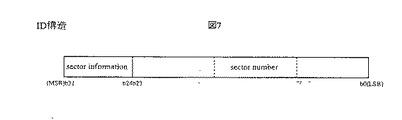
図7は、IDの構造を示した図である。IDは、1バイトのsector informationと、3バイトのsector numberから成る。sector numberは、当該セクタがデータの先頭からいくつ目に在るかを示すセクタ固有の番号(セクタアドレス)であり、データ先頭のセクタアドレスより、セクタアドレスは1ずつインクリメントしていく。
【0024】
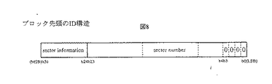
図8は、ブロック先頭のIDの構造を示した図である。データの先頭から連続する16セクタずつを集めて、1ブロックを成す。そのため、ブロックの先頭のセクタアドレスは、2進法であらわすと、最下位bitは、常に0000bとなる。
【0025】
以下、ブロック先頭の検出方法を説明する。
【0026】
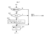
復調手段は、各ビット毎に、連続した入力信号のパターンが予め規格により規定されたパターンの同期信号であるかを判定する。同期信号を検出すると、そこからセクタアドレスの位置を求め、セクタアドレスを検出する。ディスクより再生される連続したセクタデータに対し、セクタアドレスは、連続のものであるので、予めマイコンより設定された値以上のセクタアドレスの連続が確認され、かつ、そのセクタアドレスの最下位bitが、0000bであると、復調手段は、そのセクタをブロック先頭であると判定する。セクタアドレスや同期信号が、破壊されていて、セクタアドレスが読み取り不可能の場合、復調手段は、一つ前のセクタアドレスから現在のセクタアドレスを内挿する。内挿されたセクタアドレスの回数が予めマイコンから設定された値以上になると、そのセクタアドレスの下位4bitが0000bであっても、ブロックの先頭であると判断しない。
【0027】
以上、この方式を採用することによって、正常なデータのブロック先頭のみを検出し、誤り訂正開始信号を正確に発生することが出来る。
【0028】
以下、 復調手段の内部動作について詳しく説明する。尚、復調手段の詳細説明では、図11に示されるフォーマットに従ったデータが入力される場合を前提とする。
【0029】
入力データのフォーマットについて説明する。図11は図6に示されるデータの斜線部を8−16変調したものを示す。182バイト毎に32ビットの同期信号が付加され1488ビットのフレームが構成される。同期信号は上位16ビットに0から7迄の8種類のコードが付加され、下位16ビットには所定の信号の並びが付加されている。
【0030】
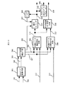
図12は図1に示されるディスク再生装置の復調手段8の構成例を示した図である。図12において、101は図11において示される同期信号を検出し、sync取込みタイミング信号102を発生する同期検出手段である。103は、同期検出状態を示すsyncフラグであり、104は同期検出手段101にてシリアル/パラレル変換されたパラレルデータであり、105は8−16変調則に従い復調する復調回路である。106は復調後のデータである。セクタ内位置検出手段107は同期検出手段101にて生成されたsync取込みタイミング信号102により、復調後のデータ106から同期信号を抜き出し内部信号syncコードを生成する。又、セクタ内位置検出手段107はsyncコードよりセクタ内の位置を示す位置コード及び位置コードよりセクタ先頭を検出しセクタアドレス取込みタイミング信号108を生成する。109は位置コード検出状態を示すセクタ内位置フラグである。セクタアドレス検出手段110はセクタアドレス取込みタイミング信号108に従ってセクタアドレス検出を行う。111はセクタアドレス検出手段110にて検出された検出処理後のセクタアドレスであり、112はセクタアドレスの誤りの有無を示すセクタアドレスステートであり、セクタアドレスに誤りがある場合を0、誤りが無い場合を1とする。113はセクタアドレス検出状態を示すセクタアドレスフラグである。ブロック先頭検出手段114は検出処理後のセクタアドレス111の値及びセクタアドレスステート112を判定しブロック先頭の検出を行う。11はブロック先頭検出信号である。115はブロック先頭検出状態を示すブロック先頭フラグである。116は出力制御を行う出力手段であり、出力制御の方法については以下に説明する。syncフラグ103、セクタ内位置フラグ109、セクタアドレスフラグ113、ブロック先頭フラグ115の値より全てが0の時データ転送可とする。どれか1つが1の時、又は直前のデータが誤りを含まずデータ転送可であればデータ転送可、直前のデータが誤りを含みデータ転送不可であればデータ転送不可とする。どれか1つが2の時データ転送不可とする。データ転送不可からデータ転送可となるのは全てが0となってからとする。以下の説明において、各フラグの値は上述したデータ転送の状態を示す。
【0031】
以上の動作を図13のタイミングチャートにより説明する。図13では上述した動作をタイミングチャートにより示したものである。同期検出手段101において、設定された回数同期信号が連続して検出(図12では1連続と仮定)されるとsyncフラグ103は2から0となる。セクタ内位置検出手段107において同期信号よりセクタ内位置検出手段の内部信号であるsyncコード151が生成される。syncコード151は各フレーム毎に図13に示す通りに当てはめられているものとする。syncコード151の連続した値(図13ではsyncコード151の3連続の値)によりフレームを分割(図13では26分割)しそれぞれの位置を示すセクタ内位置検出手段107の内部信号である位置コード152が生成される。syncコード151の連続した値から位置コード152を生成する方式について説明する。 syncコード151は0〜7の8通りの値をもち1セクタ26フレームの各連続する3つのフレームのsyncコード151の組み合わせに同じ組み合わせはない。従って、図13に示した様に例えばsyncコード151が2−7−3の連続した値をとる場合には位置コード151に22をデコードさせるようにすればフレーム毎に位置コード152を割り当てることが可能である。syncコード151の3連続の値は唯一箇所のフレームの位置を表すので位置コード152の重複を避けることができる。フレームの位置を示す位置コード152の生成方式についてはこれに限定されるものではなく、例えばsyncコード151の2連続の値により位置コード152を生成させ、重複のあるsyncコード151の連続した値だけ3連続の値を判定させる方式をとることも考えられる。
【0032】
連続した値の検出が設定数以上連続して検出されると、セクタ内位置フラグ109は2から0となる。セクタ内位置コード109が0である場合、即ちセクタの先頭を示す場合、復調後のデータ106に含まれるセクタアドレスを取り込む。復調後のデータ106内のセクタアドレスが正規データである場合即ち誤りを含まない場合にはセクタアドレスステート112がセクタアドレスが有効なデータである事を示す値である1となる。図13においては、最初のセクタアドレス(1111b)で正規データ即ち誤りを含まないデータが取込めた事を示す。誤りを含まないセクタアドレスが設定数以上連続して検出(図13では1連続)されるとセクタアドレスフラグ113は2から0となる。このセクタアドレスの値が0000b且つセクタアドレスステートが有効を示す状態かを判定し、ブロック先頭信号11を生成する。最初に取り込んだセクタアドレスにおいてはセクタアドレスステート112が有効即ちセクタアドレスに誤りを含まない状態である事を示しているが、セクタアドレスが0000bでない為ブロック先頭信号11は生成されない。次のセクタにおいては、セクタアドレスが0000bであり且つセクタアドレスが有効データと判断されるのでブロック先頭信号が生成されブロック先頭フラグ115は2から0となる。
【0033】
連続検出により連続性による保護を同期検出手段101で行い、更に図11の示される同期信号により生成されるセクタ内の位置コード151はコードの連続性により保護され、セクタ内位置コードで示されるセクタの先頭で取込むセクタアドレスも連続性で保護されている。従って検出処理後のセクタアドレス111によりブロック先頭検出を行うことにより、フォーマットに従った正常なデータの入力に対して確実にブロック先頭のみを検出することができる。又、図11に示される同期信号、セクタ内の位置コード151、検出処理後のセクタアドレス111の連続性判定による保護はそれぞれ連続回数を設定できるので、システムによって保護の確実さとブロック先頭の検出の迅速さを切り換えられる。
【0034】
以下、各検出手段の詳細を説明する。
【0035】
次に図12に示される同期検出手段101の構成例について説明する。図14は図12に示される同期位置検出手段101の回路構成例を示す。同期検出手段101の構成例を図14に示す。図14において、201はシリアルデータをパラレルデータに変換し、同期信号の検出を行う同期判定手段であり、203は同期検出信号である。204は再生クロック6をカウントするwindowカウンタであり、205はwindowカウンタ204の値である。206はマイコンにからの制御信号で、同期信号を取り込むタイミング信号であるwindowの開閉を設定するwindow設定値であり、207はwindowカウンタの値205、window設定値206に応じて同期信号を取り込むwindow開放命令208、window閉鎖命令209を生成するデコーダである。210はwindow開放命令208、window閉鎖命令209の値に応じてwindow211を開閉するwindow制御である。212は同期検出信号203、window211により正規の同期信号が検出されたことを示す信号、正規検出信号213を生成する検出判定手段である。214はマイコンからの制御信号で、同期信号連続検出回数の制御をするためのsync検出回数設定値である。215はsync検出判定手段であり同期信号連続検出回数を数える検出カウンタ、sync検出回数設定値214と検出カウンタの値を比較するデコーダにより構成されている。216は連続検出信号である。217はsyncフラグ判定手段でありsync検出設定値214及び連続検出信号216によりsyncフラグ103を生成する。218はマイコンからの制御信号で、同期信号の連続非検出回数の制御をするためのsync非検出回数設定値である。219はsync非検出判定手段であり同期信号連続非検出回数の非検出カウンタ、sync非検出回数設定値218と非検出カウンタの値を比較するデコーダにより構成されている。220は連続非検出信号である。221はsync判定手段でありsync非検出設定値218と連続非検出信号220によりsync判定信号222を生成する。223は補完制御手段であり、補完カウンタ、デコーダにより構成されている。223は補完制御手段である。
【0036】
図15、図16、図17を用い回路動作を説明する。図15、図16、図17は図14の示される同期検出手段のフローチャートである。
【0037】
図11のフォーマットに従った誤りのないデータが連続して入力されている場合の動作について説明する。同期判定手段201においてシリアルデータはパラレルデータ202に変換され、図11に示される同期信号が検出された場合には同期検出信号203を生成する(2002)。次にwindowカウンタ値205とwindow設定値206の値をデコーダ207にて判定する(2003)。windowカウンタ204の値が開放の値をとる場合について説明する。window開放命令208が生成されwindow判定210でwindow211が開放されwindowカウンタ204をインクリメントする(2009)し、図17(B)へ移行する。window211は図11のフォーマットに従ったエラーのないデータが連続して入力されている場合、同期信号部分で開放となり同期信号を取り込む。図17(B)以降の動作について説明する。図17(B)以降では、判定2で補完カウンタの値が1フレーム終了の値又は1つ前の同期信号でsync検出検出設定値214以上連続して同期信号が検出された場合に検出を示すsync判定信号222が検出且つ同期信号の特定の同期パターンが検出されたか判定する(2019)。入力データの前提より同期信号以外のデータの入力である為、2020の処理へ移行する。2020では補完カウンタをインクリメントし次の処理へ移行する。補完カウンタは、再生クロック数をカウントしており、このカウンタ値によりフレームを管理する。シリアルデータ7は再生クロック6に同期して1ビット単位で入力されるので、1フレームの再生クロック6の数は1フレームを構成する1488ビットと同数の1488クロックである。次に、補完制御手段に含まれるデコーダで補完カウンタの値を判定し(2021)、補完カウンタの値がシリアルデータからパラレルデータに変換した同期信号を出力するタイミングとなった場合にはsync取込み信号102を生成する(2022)。2021における補完カウンタ判定で、シリアルデータからパラレルデータに変換した同期信号を出力するタイミングとならない場合には処理を終了し次の入力を待つ。window211が開放されている場合は同期信号に含まれる特定パターンの入力待ちの状態である。次にwindow211が開放で同期信号が入力された場合の動作について説明する。2003のwindowカウンタの値205の判定で同期信号が入力されるタイミングでのwindowカウンタの値205の値はwindow211の開放および閉鎖の値をとっていない為、2010の判定1へ以降する。window211が開放であり且つ同期信号に含まれる同期パターンが入力されたかを判定する。入力データの前提より現在誤りのない同期信号が入力されているのでwindow211が開放であり且つ同期信号に含まれる同期パターンが検出されている為2012へ移行する。2012では検出判定212にて、window211が開放であり且つ同期信号が検出された場合には正規検出信号213を生成し、window211を閉鎖、windowカウンタ204をリセット、非検出カウンタをリセットする。次に2013で1つ前の同期パターンで連続して同期パターンが検出された回数がsync検出設定値214以上検出された場合検出を示すsync判定信号222の判定を行う。入力データは誤りのないデータが連続して入力されていることを前提としているのでsync判定信号222は検出を示している為2014へ移行する。2014ではsync判定検出に含まれる同期パターンの連続検出回数をカウントする検出カウンタをインクリメントし、その後検出カウンタの値を判定する(2015)。検出カウンタの値がsync検出設定値214以上であればsync判定信号222を検出(2017)としsyncフラグ103を0とし(2018)図17(B)へ移行する。図17(B)以降の動作は同一である。
【0038】
次に1つ前の同期信号まで誤りを含まず現同期信号に誤りが含まれるデータの入力に対する動作について説明する。誤りを含む同期信号が入力された場合、2002の処理は同一である。2003のwindowカウンタの値205の判定でwindow211を開放する値となった場合2009以降の動作はデータに誤りを含まない場合の動作と同一である。次にwindowカウンタの値205が開放及び閉鎖の値を示さない場合について説明する。2003のwindowカウンタの値205の判定により2010へ移行する。2010の判定ではwindow211は開放となっているが入力データの前提より同期パターンが検出されない為2011の処理へ移行する。windowカウンタ204をインクリメントし(2011)図17(B)へ移行する。図17(B)以降の動作についてはデータに誤りを含まない場合の動作と同一である。前記動作はwindowカウンタ24の値が閉鎖の値を示すまで同一である。windowカウンタ204の値が閉鎖の値をとる場合について説明する。2003のwindowカウンタの値205の判定で、windowカウンタの値205が閉鎖の値をとる場合について説明する。2003の判定により図16(A)へ移行する。図16(A)以降の動作について説明する。window閉鎖命令209が生成されsync検出判定手段215に含まれる同期信号の連続検出数をカウントする検出カウンタをリセットし(2004)、非検出判定手段に含まれる同期信号の連続非検出回数をカウントする非検出カウンタをインクリメントする(2005)。次に、非検出カウンタの値を判定し(2006)する。前提としたデータの入力の場合sync非検出設定値218が2以上である場合にはsyncフラグ103を1とし(2007)、図17(B)へ移行する。前提としたデータの入力の場合2006の非検出カウンタの判定でsync非検出回数設定値218が例えば1である場合にはsync判定信号222を非検出、syncフラグを2とし(2008)図17(B)へ移行する。図17(B)以降の動作についてはデータに誤りを含まない場合の動作と同一である。
【0039】
次に連続して同期信号が誤りを含むデータの入力に対する動作について説明する。この場合の動作は1つ前のデータ迄誤りを含まず現同期信号に誤りが含まれている場合の動作と同一である。図16(A)の2005迄の動作は1つ前の同期信号迄誤りを含まず現同期信号に誤りが含まれるデータの入力に対する動作と同一である。図16(A)以降の動作について説明する。非検出カウンタの値を判定し(2006)、連続非検出回数がsync非検出設定値218以下である場合にはsyncフラグ103を1とし(2007)、図17(B)へ移行する。非検出カウンタの値が連続非検出のsync非検出回数設定値218以上と判定(2006)された場合にはsync判定信号222を非検出、syncフラグを2とし(2008)図17(B)へ移行する。(B)以降の動作は1つ前の同期信号まで誤りを含まず現同期信号に誤りが含まれるデータの入力に対する動作と同一である。
【0040】
次に、1つ前の同期信号迄誤りを含んでおり現同期信号で誤りを含まないデータの入力に対する動作について説明する。2003のwindowカウンタの判定においてwindowカウンタの値205が開放の値をとる場合はデータに誤りを含まない場合の動作と同一である。同期信号が入力された場合について説明する。図15の2012迄連続してデータに誤りを含まないデータに対する動作と同一である。2013で1つ前の同期パターンで連続して同期パターンが検出された回数がsync検出回数設定値214以上検出された場合検出を示すsync判定信号222の判定を行う。前提としているデータは1つ前の同期信号に誤りが含まれている為sync判定信号222は非検出を示すので2014へ以降する。検出カウンタをインクリメントし、その後検出カウンタの値を判定する(2015)。検出カウンタの値がsync検出回数設定値214以上即ち前提としたデータの入力に対し、sync検出回数設定値が1である場合sync判定信号222を検出(2017)としsyncフラグ103を0とし(2018)図17(B)へ移行する。検出カウンタの値がsync検出設定値214以下即ち前提としたデータの入力に対し、sync検出回数設定値が2である場合であればsyncフラグ103を1とし(2018)図17(B)へ移行する。図17(B)以降の動作はデータに誤りを含まない場合と同一である。
【0041】
図17に示すフローの補完動作により同期信号が検出されない場合においてもsync取込みタイミング信号102を生成することができる。又、1つ前の同期信号検出が非検出状態で補完カウンタの値が1フレーム終了の値以下であっても、同期信号を検出すると補完カウンタをリセットしその同期信号を基点として以降検出を続ける。以上の方式により生成されたsync取込みタイミング信号102は、セクタ内位置検出手段へ送られる。
【0042】
次に図12に示されるセクタ内位置検出手段107の構成例について説明する。図18は図12に示されるセクタ内位置検出手段107の回路構成例を示す。図18において301はsync取込みタイミング信号102に従って復調データ106から抽出した同期信号を変換するsyncコード変換手段であり、302はその変換コードであるsyncコードであり、303は変換コードの有効及び無効を示す信号であるsyncコード判定信号である。304はsyncコードのp(p:自然数)値連続の並びにより検出位置コード305を生成するセクタ内位置検出手段である。306は検出位置コードが有効であることを示す検出位置コード有効信号であり、307は検出位置コードが無効であることを示す検出位置コード無効信号である。308位置コード検出判定手段でありカウンタ及びデコーダで構成されている。309は非検出判定手段でありカウンタ及びデコーダにより構成されている。310はマイコンからの連続検出回数の制御を行う為の位置コード検出回数設定値であり、311はマイコンからの連続非検出回数の制御を行う為の位置コード非検出回数設定値である。312は検出位置コードが検出回数設定値310以上連続して検出位置コード305が検出されたことを示す検出位置コード検出信号である。313は検出位置コードが非検出回数設定値311以上連続して検出位置コード305が検出されなかったことを示す検出位置コード非検出信号である。314は検出位置コードの補完を行う補完カウンタであり、315は位置コードである。316は位置コードの値によりカウンタのリセットを制御するリセット信号317を生成するデコーダである。318はセクタ内位置フラグをの切り換えを行うセクタ内位置フラグ判定手段であり、109はセクタ内位置フラグである。319はセクタアドレス取込みタイミング信号108を発生するデコーダである。
【0043】
図19、図20、図21、図22及び図23を用い回路動作を説明する。図19、図20、図21、図22及び図23は図18のセクタ内位置検出手段の動作を示したフローチャートである。
【0044】
図11のフォーマットに従った誤りのないデータが連続して入力されている場合について説明する。syncコード変換手段301において、上述した図12に示す同期信号検出手段101で生成されたsync取込みタイミング信号102により復調データ106から同期信号を取込む(3002)。取込んだsyncコードを変換し、syncコード302を生成する(3003)。次にセクタ内位置検出304においてsyncコード302のp(p:自然数)値連続の値により検出位置コード305を生成する(3004)。検出位置コード305はセクタをsyncコード302の連続した値よりq(q:自然数)分割し、それぞれのフレームに割り当てたコードである。syncコード302の連続した値が予測される連続した値に対応すれば図20の(A)へ移行する(3005)。図20(A)以降の動作について説明する。非検出判定309に含まれる連続非検出数をカウントする非検出カウンタをリセットする(3006)。次に位置コード検出信号312の判定を行う(3007)。検出位置コード検出信号312は、直前の検出位置コード305の状態を示しており、1の時検出を示し、0の時非検出を示すものとする。誤りのないデータが連続して入力されていることが前提となっているので位置コード検出信号312は検出である1を示す。検出信号が1を示す場合には既に1つ前の判定において連続検出数が位置コード検出設定値310以上となった事を示す為次の処理へ移行する。位置コード検出判定手段308にて検出カウンタ値と位置コード検出設定値310の比較を行う(3009)。3009の検出カウンタの判定で検出カウンタの値が位置コード検出回数設定値310以上となった場合は検出信号を1(3010)とし図22の(C)、(D)へ移行する。
【0045】
図22の(C)以降について説明する。(C)以降では検出位置コード検出信号312及び検出位置コード非検出信号313によりセクタ内位置フラグ109をセクタ内位置フラグ判定手段318にて切替えを行う(3012)。検出位置コード非検出信号313は、1の時非検出であることを示し、0の時検出を示す。検出位置コード検出信号312が1且つ検出位置コード非検出信号313が0を示す場合即ち検出位置コード305が連続して設定値以上検出された場合セクタ内位置フラグ109を0(3012a)、検出位置コード検出信号312が0且つ検出位置コード非検出信号313が1を示す場合即ち検出位置コード305が位置コード検出設定値310以下で連続して検出されていない状態又は位置コード非検出設定値311以下で連続して非検出状態の場合セクタ内位置フラグ109を1(3012b)、検出位置コード検出信号312が0且つ検出位置コード非検出信号313が1を示す場合セクタ内位置フラグ109を2(3012c)とする。
【0046】
(D)以降の処置では、先ず、検出位置コード検出信号312が検出を示すか判定を行う(3013)。前提とした入力データにおいては検出位置コード検出信号312が1を示す為、syncコードの連続値によって生成された検出位置コードを補完カウンタにロードする(3014)。出力形態としては、この場合は検出位置コード検出信号により検出位置コードをカウンタにロードしカウンタの出力を位置コードとしているが出力方式については限定しない。次に位置コード315が先頭を示す値となっているかの判定を行う(3018)。先頭を示す値であればセクタアドレス取込みゲートデコーダ319においてセクタアドレス取込みタイミング信号108が生成される(3019)。先頭以外の値であればセクタアドレス取込みタイミング信号108は生成されない(3020)。尚、セクタアドレス取込みタイミング信号108の生成はこの手法に限定されるものではなく、例えば位置コードを直接セクタアドレス検出手段へ送りそこで位置コードの値よりセクタの先頭を判定しセクタアドレスを取込む手法を取っても同様の結果が得られる。
【0047】
次に1つ前の同期信号まで誤りが含まれず現同期信号に誤りが含まれるデータの入力に対する動作について説明する。図19のフローチャートの3004迄の処理はデータに誤りを含まない場合と同一である。3005のsyncコード302の連続した値の判定で現同期信号に誤りが含まれている為連続した値が予測される値と対応しない為図21(B)へ移行する。図21(B)以降の動作について説明する。位置コード検出判定手段308に含まれる検出カウンタをリセットする(3021)。次に検出位置コード非検出信号313の判定を行う(3022)。検出位置コード非検出信号313は直前の検出位置コードの状態を示しており、1の時非検出を示し、0の時検出を示すものとする。現在の検出位置コードが無効即ち非検出である為、位置コード非検出判定309に含まれる非検出カウンタをインクリメントする(3023)。次の処理では非検出カウンタの判定を行う。位置コード非検出判定手段309にて非検出カウンタ値と位置コード非検出回数設定値311の比較を行い(3024)、非検出カウンタの値が位置コード非検出設定値311以下である場合検出位置コード非検出信号313を0(3025)とし図22の(C)、(D)へ移行する。図22(C)以降の動作はデータに誤りを含まない場合と同一である。図22(D)以降の動作について説明する。検出位置コード検出信号312が検出を示すか判定を行う(3013)。前提としているデータは現同期信号に誤りが含まれている為検出位置コード検出信号312は無効である0を示す為3015へ移行する。3015では直前の位置コードの値を判定する。直前の位置コードがq分割された値の最終値以下であった場合は補完カウンタ314の値をインクリメント(3016)し位置コードとする。最終値を示す場合にはデコーダ316により補完カウンタ314のリセット信号317を生成し補完カウンタ314をリをセットしその値を位置コードとする(3017)。3018以降の動作についてはデータに誤りを含まない場合の動作と同一である。
【0048】
次に同期信号に誤りを含むデータが連続して入力された場合の動作について説明する。この場合の動作は現同期信号が誤りを含む場合と同一である。
【0049】
次に1つ前の同期信号迄誤りを含み現同期信号で誤りを含まないデータの入力に対する動作について説明する。図19の3002から図20の3006迄の処理はデータに誤りを含まないデータの入力に対する動作と同一である。3007以降の動作について説明する。次に検出位置コード検出信号312の判定を行う(3007)。検出位置コード検出信号312は、直前の検出位置コード305の状態を示しており、1の時検出を示し、0の時非検出を示すものとする。検出位置コード検出信号312が0即ち直前の検出位置コード305で位置コード検出回数設定値310以上連続して検出位置コードが検出されていない場合、現在の検出位置コードが有効である為、位置コード検出判定手段308に含まれる連続検出数をカウントする検出カウンタをインクリメントする。即ち、連続検出回数に加える(3008)。3007の検出位置コード検出信号312判定で、検出信号が1を示す場合には既に1つ前の判定において連続検出数が位置コード検出回数設定値310以上となった事を示し処理へ移行する。位置コード検出判定手段308にて検出カウンタ値と位置コード検出設定値310の比較を行い(3009)、検出カウンタの値が位置コード検出設定値310以下である場合には検出位置コード検出信号312を0とし(3011)図22の(C)、(D)へ移行する。3009の検出カウンタの判定で検出カウンタの値が位置コード検出設定値310以上となった場合は検出信号を1(3010)とし図22の(C)、(D)へ移行する。
【0050】
図(C)、(D)以降の動作は同期信号に誤りを含むデータが連続して入力された場合と同一である。
【0051】
以上の方法により生成されたセクタアドレス取込みゲートはセクタアドレス検出手段へ送られる。
【0052】
次に図12に示されるセクタアドレス位置検出手段110の構成例について説明する。図24は図12に示されるセクタ内位置検出手段110の回路構成例を示す。図24において、セクタアドレス判定手段401はセクタアドレス取込みタイミング信号108により復調データ105内に含まれるセクタアドレスを抜き出し、現在のセクタアドレスの状態を示す信号402及び1つ前のセクタアドレスの状態を示す信号403を生成する。404はセクタアドレスである。405は正規のセクタアドレスがロードされるマスターカウンタであり、406はマスターカウンタ405の値を示す。407は現在のセクタアドレスの状態を示す信号402、直前のセクタアドレスの状態を示す信号403、セクタアドレス404及びマスターカウンタの値406によりマスターカウンタ405のロード信号408、セクタアドレス検出信号409、セクタアドレス非検出信号410を生成するデコーダである。411はマイコンからの連続検出回数制御の為のセクタアドレス検出回数設定値であり、412はマイコンからの連続非検出回数制御の為のセクタアドレス非検出回数設定値である。413はセクタアドレス検出判定手段であり、カウンタ及びカウンタ値とセクタアドレス検出設定値411の比較を行うデコーダにて構成されている。414はセクタアドレス検出判定手段413により生成されたマスターカウンタ405及び補完カウンタ415のロード制御信号であり、416は検出回数設定値411以上連続してセクタアドレスが検出された場合セクタアドレス検出判定手段413により生成される連続検出信号である。417はセクタアドレス非検出判定手段であり、カウンタ及びカウンタ値とセクタアドレス非検出設定値412の比較を行うデコーダにて構成されている。418は非検出回数設定値412以上連続してセクタアドレスが検出されない場合にセクタアドレス非検出判定手段417により生成される連続非検出信号である。419はセクタアドレスフラグ判定手段であり、セクタアドレスフラグ113を生成する。420はセクタアドレスの状態を判定するセクタアドレスステート判定手段であり、112のセクタアドレスの状態を示すセクタアドレスステート信号を生成する。111は検出後のセクタアドレスを示す。421はマイコンからのセクタアドレス判定制御の設定値である。
【0053】
図25、図26、図27、図28及び図29を用い回路動作を説明する。図25、図26、図27、図28及び図29は図24に示すセクタアドレス検出手段の動作を示すフローチャートである。
【0054】
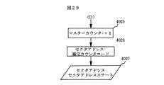
図11のフォーマットに従った誤りのない又は、IEDによりセクタアドレス404が訂正可能なデータが連続して入力された場合の動作について説明する。セクタアドレス判定手段401で図12に示すセクタ内位置検出手段107で生成されたセクタアドレス取込みタイミング信号108により復調データ106からセクタアドレスをを取込む(4001)。次にセクタアドレスの判定を行う。ここでは、セクタアドレス状態を示す値は、0:誤り無、1:誤りを含むがIEDによる訂正が可能、2:IEDによる訂正が不可能の3値をとるものとするが、判定基準及び割り当てはこれに限定しない(4002)。次にセクタアドレス判定制御421によりIEDによるセクタアドレス訂正の有無を設定する(4003)。IEDによる訂正を行う設定であればセクタアドレス判定401にて訂正を行い(4004)、IEDによる訂正を行わない設定であれば訂正しない。次にデコーダ407にて現在のセクタアドレスの状態を示す信号402の判定を行う。現在のセクタアドレスの状態を示す信号402は入力データの前提から0又は1である為次の処理へ移行する(4005)。次の処理ではセクタアドレスの連続性判定の有無の判定を行う(4006)。連続性判定無の場合にはセクタアドレス非検出判定手段417に含まれる非検出カウンタをリセットし図26(A)へ移行する(4009)。連続性判定有りの場合には直前のセクタアドレスの状態を示す信号403により直前のセクタアドレスの状態判定を行う。(4007)。直前のセクタアドレスの状態を示す信号403は入力データの前提より0又は1を示す為処理4008へ移行する。4008ではセクタアドレス404とマスターカウンタ値406をデコーダ407で比較を行う。入力データの前提からセクタアドレス404とマスターカウンタ値406は一致するので、非検出カウンタをリセットし図26(A)へ移行する(4009)。次に図26の(A)以降の処理について説明する。(A)に移行するのは、1つ前のセクタアドレス及び現在のセクタアドレスが誤りを含まない又はIEDによる訂正が可能な場合である。検出カウンタをインクリメント即ち現在処理中のセクタアドレスを連続検出としてカウントし(4011)、セクタアドレス検出判定手段413において検出カウンタの値とセクタアドレス検出設定値411の比較を行い(4012)、現在処理中のセクタアドレス404で連続検出数がセクタアドレス検出設定値411以上である場合にはマスターカウンタ405、補完カウンタ415へ取込んだセクタアドレス404をロードする。この時、IEDによる訂正有りが選択されている場合にはIEDによる訂正済みのセクタアドレス404がロードされる(4013)。その後、セクタアドレスフラグ判定手段419によりセクタアドレスフラグ113を0(4014)、セクタアドレスステート判定手段420によりセクタアドレスステート112を有効とし(4015)、図29の(D)へ移行する。図29(D)以降の処理では、マスターカウンタ405をインクリメントし(4025)、補完カウンタの値をセクタアドレスとして(4026)、検出処理後のセクタアドレス111、セクタアドレスステート信号112を出力する(4027)。
【0055】
次に1つ前のセクタアドレス迄誤りが含まれず現セクタアドレスに誤りが含まれ且つIEDによる訂正が不可能なデータの入力に対する動作について説明する。図25の4004迄の処理は誤りを含まないデータの入力に対する動作と同一である。4005の判定で現セクタアドレスはIEDによって訂正が可能でる為現在のセクタアドレスの状態を示す信号402は2を示す為4010の処理へ移行する。4010では検出カウンタをリセットし図27(B)へ移行する。図27(B)以降の動作について説明する。先ず、連続性判定の有無を判定する(4016)。連続性判定が無しである場合は補完カウンタ415をインクリメントし図28(C)へ移行する(4019)。連続性判定有りの場合は直前のセクタアドレスの状態を示す信号403を判定する(4017)。1つ前のセクタアドレスの状態を示す信号が2即ちIEDによる訂正が不可能である場合は補完カウンタ415をインクリメントし図28(C)へ移行する(4019)。1つ前のセクタアドレスの状態を示す信号403が0又は1即ち誤り無し又はIEDによる訂正が可能である場合はマスターカウンタ405に現在のセクタアドレス404をロードする(4018)。その後、補完カウンタをインクリメントし図28(C)へ移行する。図28(C)以降の動作について説明する。セクタアドレス非検出判定手段417に含まれる非検出カウンタをインクリメントする(4020)。次に非検出カウンタの値とセクタアドレス非検出設定値412をセクタアドレス非検出判定手段417に含まれるデコーダにて比較する(4021)。非検出カウンタの値がセクタアドレス非検出設定値412以上である場合にはセクタアドレス非検出手段417にてセクタアドレス非検出信号418を生成しセクタアドレスフラグ判定手段419でセクタアドレスフラグ113を2とする(4022)。次にセクタアドレス非検出信号418によりセクタアドレスステート判定手段420でセクタアドレスステート112を無効とし(4023)図29(D)へ移行する。4021の非検出カウンタ値の判定で非検出カウンタの値がセクタアドレス非検出設定値412以下である場合にはセクタアドレスフラグ判定手段419でセクタアドレスフラグ113を1とし(4024)図29(D)へ移行する。図29(D)以降の動作はデータに誤りを含まない又はIEDによりセクタアドレス404の訂正が可能なデータの入力に対する動作と同一である。
【0056】
次にIEDによりセクタアドレス404の訂正が不可能なデータの入力に対する動作について説明する。この場合の動作は1つ前のデータに誤りを含まない又はIEDによりセクタアドレス404が訂正可能なデータの入力と同一である。
次に1つ前のデータまでIEDによるセクタアドレスの訂正が不可能なデータであり現セクタアドレス404に誤りを含まない又はIEDのよるセクタアドレス404の訂正が可能であるデータの入力に対する動作について説明する。図25の4001から4005迄はデータに誤りを含まない又はIEDによる訂正が可能であるデータの入力に対する動作と同一である。4007でセクタアドレス404の連続性を判定しない場合はデータに誤りを含まない又はIEDによる訂正が可能であるデータの入力に対する動作と同一である。セクタアドレスの連続性を判定する場合、4009に移行し直前のセクタアドレスの状態を示す信号403の判定で直前のセクタアドレス404はIEDによる訂正が不可能である為直前のセクタアドレスの状態を示す信号403は2を示している為4010へ移行する。4010移行の処理は1つ前のセクタアドレス迄誤りが含まれず現セクタアドレスに誤りが含まれ且つIEDによる訂正が不可能なデータの入力に対する動作と同一である。
【0057】
以上の動作によって正規セクタアドレス若しくは訂正可能なセクタアドレスについてはそのまま出力し、不正なセクタアドレスの入力に対しては補完値をセクタアドレスとして出力する事が出来る。セクタアドレスの下位4ビット及びセクタアドレスステートはブロック先頭検出手段へ送られる。
【0058】
次に図12に示されるブロック先頭検出手段114の構成例について説明する。図30は図12に示したブロック先頭検出手段114の回路構成例である。図30において501は連続非検出制御のためのブロック先頭非検出設定値である。502は判定デコーダであり、503はセクタ数をカウントするカウンタである。504はカウンタ503の値であり、505はセレクト信号である。506はカウンタのリセット信号である。507はフラグ制御信号である。508はカウンタ503にロードする値を505によって切り替え、セレクトデータ509を生成するセレクタである。510はカウンタの値504及びフラグ制御信号507によりブロック先頭フラグ115を切り替えるブロック先頭フラグ判定手段である。115はブロック先頭フラグであり11はブロック先頭検出信号である。
【0059】
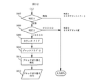
図31、図32及び図33を用い回路動作を説明する。図31、図32及び図33は図30に示されるブロック先頭検出手段の動作をフローチャートにより示したものである。図12に示されるセクタアドレス検出手段110にて生成されたセクタアドレス111及びセクタアドレスステート112を判定デコーダ502に取込む(5002)。次にブロック先頭フラグの判定を行う。この時、ブロック先頭フラグ115の値が2であれば図32の(A)へ移行する(5003)。0又は1をとる場合はカウンタ503をインクリメントし(5004)、カウンタ値の判定を行う(5005)。カウンタ503はブロック内のセクタ数をカウントするカウンタであり1度ブロックの先頭を検出したところからインクリメントを開始する。このカウンタの値が16未満である場合には次のセクタアドレスの入力を待つ(5005)。
【0060】
カウンタ値が16以上の値をとる場合については、正常なデータの1ブロックは16個のセクタにより構成されている為にカウンタの値が16である時ブロックの先頭が来ると予測される。カウンタ値が16であれば図32の(A)へ移行する。1以上の値をとれば図33の(B)へ移行する(5006)。
【0061】
次に図32の(A)以降の動作について説明する。先ずセクタアドレスステート112を判定する。セクタアドレスステートが無効であることを示す場合は次の入力を待ち、有効であれば次の処理へ移行する(5007)。次に検出処理後のセクタアドレス111の値を判定する。1ブロック16セクタであるので1ブロック内でセクタアドレスの下位4ビットは2進数で0000b〜1111bの間で推移する。従って、ブロックの先頭のセクタアドレスの下位4ビットは0000bである。検出処理後のセクタアドレス111の値が0000b即ちブロックの先頭を示す検出処理後のセクタアドレス111でなければ次の入力待ちとなり、検出処理後のセクタアドレス111が0000bであれば次の処理へ移行する(5008)。従って、次の処理へ移行するのはセクタアドレスステート112が有効であり且つセクタアドレスが0000bである場合即ちブロック先頭を検出した場合である。カウンタ503をリセットし(5009)、ブロック先頭フラグ判定510でブロック先頭フラグを0とし(5010)、デコーダ502でブロック先頭を検出し(5011)、ブロック先頭検出信号11を出力する(5012)。
【0062】
図33(B)以降の処理について説明する。図33(B)へ以降するのは5006のカウンタ503判定でカウンタ503の値が17以上を示した場合即ちブロック先頭が検出されなかった場合である。カウンタ503の値がブロック先頭非検出設定値501を比較し(5014)カウンタ503の値と設定値501が一致した場合、カウンタ503をホールドし(5016)、ブロック先頭フラグを2として次の入力待ちとなる(5016)。
【0063】
5014のカウンタ503の判定でカウンタ503の値が設定値501以下であった場合、セクタアドレスステート112の判定を行う(5017)。セクタアドレスステート112が無効であった場合、ブロック先頭フラグを1とし(5018)次の入力待ちとなる。5017のセクタアドレスステート112判定でセクタアドレスステート112が有効を示す場合はカウンタ503に検出処理後のセクタアドレス111をロードし(5019)、ブロック先頭フラグを0とし(5020)、ブロック先頭を検出し(5021)、ブロック先頭検出信号11を出力する(5022)。従って、ブロックの先頭が検出されない場合には次の有効なセクタアドレスが入力されたところ即ちセクタ先頭でブロック先頭検出信号を生成する。セクタアドレスステートが無効であればフラグ制御信号によりフラグ判定においてブロック先頭フラグを1とし次の入力を待つ。
【0064】
以上この方式を採用し、連続して検出された信号によりブロック先頭検出を行うことによって確実にブロック先頭検出が行え、正確な誤り訂正開始信号を発生することができ、復調手段にてブロックを管理することができる。又、各検出手段で連続検出数設定値及び連続非検出数設定値を切り替え、補完動作によりブロック先頭検出を行うことができる。
【0065】
従って、正常なデータのブロック先頭のみを検出し、誤り訂正開始信号を正確に発生することができる。
【0066】
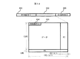
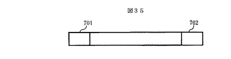
次に図34のフォーマットに従ったデータの入力に対する動作について説明する。図34について説明する。601は付加データ1であり602はデータ領域である。602のデータ領域に収められるデータフォーマットは603でありこれは図5に示すセクタ構造に付加データ及び主データに付加された列方向の誤り訂正符号PO、付加データ及び主データ及びPOに付加された行方向の誤り訂正符号を付加したフォーマットである。605の付加データは図7のセクタ構造と同一である。606は付加データ2である。601の付加データ1の構造を図35に示す。701はセクタ番号であり、702は同期信号である。図34及び図36に示すフォーマットに従ったデータが連続して入力されることを前提とする。
【0067】
図34及び図35に示されるデータは図35に示される付加データ1構造に示されるセクタ番号701により管理されており、ブロック先頭であることをセクタ番号701により検出すると図7に示されるID構造のsector numder(セクタアドレス)を全て0に置き換える。その後順次インクリメントした値を埋め込む。セクタアドレスを埋め込まれたデータは図1に示される復調手段8に入力される。復調手段8では、図5及び図6に示されるデータの入力に対する場合と同様の各検出動作を行う。図12に示されるブロック先頭検出手段114においてはセクタアドレス111及びセクタアドレスステート112によりブロック先頭の検出を行うが、図34に示されるフォーマットに従ったデータの入力の際は図32に示される5007のセクタアドレスステート判定を無視し、5008のセクタアドレス値判定のみでブロック先頭を検出するモードに切り替える事が可能である。
【0068】
以上の方式をとることにより実際にはセクタアドレス114の値が0000bでないセクタをブロック先頭として扱う場合においてもブロック先頭検出信号11を生成することができる。従って、図34及び図35に示される様な断続したデータの入力に対しても確実且つ正確にブロック切替信号11を生成することができる。又、図34及び図35に示すデータフォーマットに限らずデータが媒体上に間欠的に再生された場合の再生信号についても前記動作により確実且つ正確にブロック先頭検出信号11を生成することができる。
【0069】
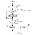
次に、図4を用いて説明したRAM12のRAMマップを更に詳しく説明する。図36は、図4と同じく14個のブロックのデータが一時記憶される。各ブロックのデータは、図6に示す構造を持つ。データは図4の説明と同じく、まず1ブロックRAM12に書き込まれる。図4で示すところのアドレス0000から書き込まれるとする。この場合1ブロックの内メインデータは、メインデータブロック1のエリア(3501)、メインデータに付加されたPIコードは、PIコードブロック1のエリア(3502)、メーンデータに付加されたPOコードは、POコードブロックaのエリア(3529)、POコードに付加されたPIコードは、PIコードブロックa(3530)のエリアにそれぞれ書き込まれる。図4の説明に記載されたように、次のブロックの復調が開始されると前のブロックのデータの誤り訂正が始まる。即ち、次のブロックの復調データのうちメインデータは、メインデータブロック2のエリア(3503)、メインデータに付加されたPIコードは、PIコードブロック2のエリア(3504)、メーンデータに付加されたPOコードは、POコードブロックbのエリア(3531)、POコードに付加されたPIコードは、PIコードブロックb(3532)のエリアにそれぞれ書き込まれる。誤り訂正はエリア(3501)(3502)(3529)(3530)のデータに対して行われる。なお、誤り訂正1ブロックの処理時間は、復調1ブロックの処理時間より短い場合を考える。更に次の復調データは、ブロック3及びブロックcの各エリア(3505)(3506)(3533)(3534)に書き込まれると同時にブロック2及びブロックbの各エリア(3503)(3504)(3531)(3532)の誤り訂正処理が行われる。更に次のデータが復調されるとブロック4及びブロックaの各エリアに書き込まれ、誤り訂正処理はブロック3及びブロックcのデータに対して行われる。上記の説明の通り、1ブロックのデータに対し、POとPOに付加されたPIは、3ブロック分のリング状のバッファ(3529)から(3534)を用いて図4で説明された処理が行われる。一方、メインデータとメインデータに付加されたPIは14個分のブロックバッファエリア3501から3528をリング状のバッファとして図4で説明された処理が行われる。PO及びPOに付加されたPIを記憶するエリアの方が小さいため、訂正処理が終了した後、外部へデータを出力する前にPO及びPOに付加されたPIは、後から復調によって書き込まれるデータによって上書きされる可能性がある。しかし、外部へのデータ出力は、メインデータのみ必要であって、訂正処理終了後はPI、POは必要ないため問題ない。図36のRAMマップでは、PI用のエリアは14ブロックとしているが、上記の理由によって3ブロック分としても構わない。(例えば3502、3504、3506だけにする)しかし、復調から読みだされる順序とアドレス順を大きく変える必要が生じる。また、POとPOに付加されたPIは3ブロック分あるがこれにより、復調1ブロックの処理の方が誤り訂正1ブロックの処理より早くなっても1ブロック分の余裕があるので、訂正処理前のPO及びPIのエリアに復調されたデータが即時に上書きされる事はない。更に復調1ブロックの処理の方が訂正1ブロックの処理より早くなったのが一時的ならば、訂正処理は、処理速度が定常に戻った後、復調に追い付くまで複数ブロック分、連続して処理し、1ブロック分の余裕はもとに戻る。即ち図9において、復調のブロックCが訂正のブロックBより短い場合、訂正Cは、訂正Bの終了と共にはじまる。それにより復調ブロックEの開始以前に訂正ブロックCが終了すれば1ブロック分の余裕が元にもどる。従って、復調系で誤動作が生じブロックの切換が早くおきても問題ない。また、アクセス時にモーター制御がおくれて、一時的に入力周波数が高くなっても問題はない。
【0070】
アクセス時の動作に付いて説明する。
【0071】
図9は、アクセス信号が入力されたときの復調にかかる時間及び、誤り訂正にかかる時間の相対関係を示した図である。復調とはデータの復調にかかる時間を示し、訂正とは誤り訂正のかかる時間を示し、再生とは、復調、又は誤り訂正を行い、データを再生している状態を示し、アクセス状態とは記録媒体に記録されているデータを、記録されている順にではなく、順不同に再生する為に、再生するデータを探すことである。具体的には、ピックアップが記録媒体上を移動している状態である。アクセス状態中は、ブロックの復調は行われず、目的のデータが入力されるまで待つ。実施例の図9では、ブロックBの復調終了後にアクセス状態になった場合である。ブロックBの復調後、アクセス中はデータ入力が無いため、復調を行うことができない。誤り訂正は次に復調を行うブロックの先頭検出信号によって開始される。通常はアクセス中は復調されるデータの入力が無いため、ブロック先頭検出信号がなく、誤り訂正を行うことができない。
【0072】
図10は、新たなモードを設定し、アクセス中も誤り訂正を行う場合の復調にかかる時間及び、誤り訂正にかかる時間の相対関係を示した図である。アクセス時、及び、最終データの復調時に、マイコンがそのことを示す信号を出す。復調手段では、その信号を検出すると、ブロック先頭検出信号を、最後のデータの最後尾で内挿する。誤り訂正手段では、内挿されたブロック検出信号を検出すると、誤り訂正を開始する。
【0073】
以上、このモードを追加することにより、誤り訂正をアクセス中に行えるので、小容量のデータをランダムにアクセスして再生する場合、出力を速く行なうことが出来る。
【0074】
【発明の効果】
以上、本発明によれば、入力されるデータレートに同期して復調を行う。誤り訂正は、固定の周波数のクロックで行い、誤り訂正にかかる時間は最大線速度で再生した場合の復調にかかる時間よりも短い。その為、データが読み取れない場合でも、誤り訂正は復調の影響を受けることなく、信頼性を高めることが出来る。
【図面の簡単な説明】
【図1】誤り訂正のブロック図。
【図2】誤り訂正の状態遷移図。
【図3】標準速、及び、2倍速における復調にかかる時間と、誤り訂正にかかる時間の相対関係を示した図。
【図4】 RAM内のデータの配列を示した図。
【図5】データのセクタ構造の説明図。
【図6】データのECCブロックの構造の説明図。
【図7】データのIDの構造の説明図。
【図8】データのブロック先頭のIDの構造の説明図。
【図9】アクセス信号入力時の復調にかかる時間と、誤り訂正にかかる時間の相対関係を示した図。
【図10】新モードにおけるアクセス信号入力時の復調にかかる時間と、誤り訂正にかかる時間の相対関係を示した図。
【図11】8−16変調され同期信号が付加された1ブロックのフォーマット。
【図12】復調手段構成ブロック図
【図13】復調手段における信号処理タイミングチャート
【図14】同期検出手段ブロック図
【図15】同期検出手段フローチャート
【図16】同期検出手段フローチャート
【図17】同期検出手段フローチャート
【図18】セクタ内位置検出手段ブロック図
【図19】セクタ内位置手段フローチャート
【図20】セクタ内位置手段フローチャート
【図21】セクタ内位置手段フローチャート
【図22】セクタ内位置手段フローチャート
【図23】セクタ内位置手段フローチャート
【図24】セクタアドレス検出手段ブロック図
【図25】セクタアドレス検出手段フローチャート
【図26】セクタアドレス検出手段フローチャート
【図27】セクタアドレス検出手段フローチャート
【図28】セクタアドレス検出手段フローチャート
【図29】セクタアドレス検出手段フローチャート
【図30】ブロック先頭検出手段ブロック図
【図31】ブロック先頭検出手段フローチャート
【図32】ブロック先頭検出手段フローチャート
【図33】ブロック先頭検出手段フローチャート
【図34】データフォーマット
【図35】付加データ1構造
【図36】RAMマップ詳細図
【符号の説明】
1・・ディスク、2・・サーボモータ、3・・ピックアップ、4・・データ、5・・PLL、6・・再生クロック、7・・シリアルデータ、8・・復調手段、9・・サーボコントロール信号、10、16、23、24、18・・パラレルデータ、11・・ブロック先頭検出信号、12・・RAM、13・・出力手段、14・・出力OK信号、15・・データ請求信号、17・・誤り訂正手段、18・・誤り訂正終了信号、19・・復調カウンタ、20・・誤り訂正カウンタ、21・・比較手段、22・・誤り訂正開始信号、25・・マイコン、26・・アクセス信号、101・・同期検出手段、102・・sync取込みタイミング信号、103・・syncフラグ、104・・パラレルデータ、105・・復調回路、106・・復調後のデータ、107・・セクタ内位置検出手段、108・・セクタアドレス取込みタイミング信号、109・・セクタ内位置フラグ、110・・セクタアドレス検出手段、111・・セクタアドレス、112・・セクタアドレスステート、113・・セクタアドレスフラグ、114・・ブロック先頭検出手段、115・・ブロック先頭フラグ、151・・syncコード、152・・位置コード、201・・同期判定手段、202・・パラレルデータ、203・・同期検出信号、204・・windowカウンタ、205・・windowカウンタ値、206・・window設定値、207・・デコーダ、208・・window開放命令、209・・window閉鎖命令、210・・window制御、211・・window、212・・検出判定手段、213・・正規検出信号、214・・sync検出設定値、215・・sync検出判定手段、216・・連続検出信号、217・・syncフラグ判定手段、218・・sync非検出設定値、219・・sync非検出判定手段、220・・連続非検出信号、221・・sync判定手段、222・・sync判定信号、223・・補完制御手段、301・・syncコード変換手段、302・・syncコード、303・・変換コードの有効及び無効を示す信号、304・・セクタ内位置検出手段、305・・検出位置コード、306・・検出位置コード有効信号、307・・検出位置コード無効信号、308・・位置コード検出判定手段、309・・位置コード非検出判定手段、310・・位置コード検出設定値、311・・位置コード非検出設定値、312・・検出位置コード検出信号、313・・検出位置コード非検出信号、314・・補完カウンタ、315・・位置コード、316・・デコーダ、317・・補完カウンタリセット信号、318・・セクタ内位置フラグ判定手段、319・・セクタアドレス取込みゲートデコーダ、401・・セクタアドレス判定手段、402・・現在のセクタアドレスの状態を示す信号、403・・1つ前のセクタアドレスの状態を示す信号、404・・セクタアドレス、405・・マスターカウンタ、406・・マスターカウンタの値、407・・デコーダ、408・・ロード信号、409・・セクタアドレス検出信号、410・・セクタアドレス非検出信号、411・・セクタアドレス検出設定値、412・・セクタアドレス非検出設定値、413・・セクタアドレス検出判定手段、414・・ロード制御信号、415・・補完カウンタ、416・・連続検出信号、417・・セクタアドレス非検出判定手段、418・・セクタアドレス連続非検出信号、419・・フラグ判定手段、420・・セクタアドレスステート判定手段、 421・・セクタアドレス判定制御設定値、501・・ブロック先頭非検出設定値、502・・判定デコーダ、503・・カウンタ、504・・カウンタ値、505・・セレクト信号、506・・リセット信号、507・・フラグ制御信号、508・・セレクタ、509・・セレクトデータ、510・・ブロック先頭フラグ判定手段[0001]
BACKGROUND OF THE INVENTION
The present invention relates to a reproducing apparatus and a reproducing method for an optical disc on which a digital signal is recorded.
[0002]
[Prior art]
There is a compact disc (CD) as a playback device using the disc.
Disc-shaped recording media such as CDs are generally recorded by a constant linear velocity (CLV) method in order to increase the recording density. The medium recorded by the CLV method has a difference of about 2.6 times in the rotation speed between the inner circumference and the outer circumference. During reproduction, the rotation speed of the medium also varies with the movement of the pickup for reading data. Therefore, at the time of access, the maximum number of rotations of the disk changes about 2.6 times, so data cannot be reproduced until the specified linear velocity is reached. On the other hand, Japanese Patent Laid-Open No. 5-250804 controls a disk recorded in CLV at a constant rotation speed (CAV) and changes the master clock according to the pickup position. However, in this method, it is necessary to provide a rotational speed detection means in order to operate the motor at a constant rotational speed, and the configuration is complicated. In view of this, a method has been devised, as disclosed in Japanese Patent Laid-Open No. 6-89506, in which control is performed at a constant linear velocity during normal reproduction and at a constant rotational speed only during access. In this method, it is necessary to calculate the disk rotation speed and the clock frequency from the current pickup position and the pickup position after access, and to generate a clock according to the result. This increases the amount of calculation and has a drawback that the calculation may not end during access. Therefore, a means for performing demodulation and error correction using a recovered clock synchronized with the rotation of the disk using a PLL has been adopted. In this method, a clock synchronized with data is reproduced from input data, and demodulation and error correction are performed using the clock. Therefore, even during access, smooth demodulation is possible.
[0003]
[Problems to be solved by the invention]
In the above method, if data cannot be read due to a scratch on the disk or the like, clock reproduction becomes unstable, demodulation becomes unstable, and reliability of error correction processing decreases.
[0004]
[Means for solving the problems]
In the present invention, demodulation is performed with a recovered clock generated in accordance with the input rate of input data, whereas error correction is performed with a clock having a fixed frequency. A counter that is incremented by a signal that is generated when the head of the block is detected and a counter that is incremented by a signal that is generated when an error is corrected in block unit data are provided, the values are compared, and an error is determined based on the result. Means are provided for generating a signal to initiate correction. Error correction is performed in a fixed time, and is the same even if the playback speed is switched between 2 times, 4 times, and j (j: natural number) times.
[0005]
DETAILED DESCRIPTION OF THE INVENTION
An embodiment of a disk reproducing apparatus according to the present invention will be described with reference to the drawings.
[0006]
FIG. 1 is a block diagram of a disc playback apparatus. In the description of this embodiment, it is assumed that data according to the format shown in FIGS. 5 and 6 is input.
[0007]
The format of input data will be described. In FIG. 5, the data input in time series is divided into 2048 bytes, and after adding 12 bytes of additional data before the main data and 4 bytes of additional data after the main data, Data is divided into units of 172 bytes to form columns, and each column is arranged in a 12-column order, forming one sector. 16 consecutive sectors are arranged in order to constitute one block. In FIG. 6, PO is the error correction code in the column direction added to the additional data and main data, and PI is the error correction code in the row direction added to the additional data, main data, and PO.
[0008]
Hereinafter, FIG. 1 will be described. In the disk reproducing apparatus of FIG. 1,
The operation clock will be described. This disc reproducing apparatus has two clocks. A reproduction clock and a crystal clock. The recovered clock is recovered from the input data by the
[0009]
The disc is recorded at a constant linear velocity (CLV) to increase the recording density. For this reason, when the rotational speed of the disk changes during access or the like, the input rate temporarily increases or decreases, and the reproduction clock also fluctuates until the rotational speed matches the initial value after the access is completed. For this reason, demodulation is possible in advance even if the frequency of the recovered clock fluctuates up to ± 50%. If error correction of data for one block is completed faster than demodulation of data for one block at n (n: natural number) multiple speed, error correction operates with a crystal oscillation clock. Thus, error correction can be performed independently and faster than demodulation without being affected by frequency fluctuations.
[0010]
Hereinafter, the operation of the disc reproducing apparatus shown in FIG. 1 will be described in order from the input.
[0011]
The
[0012]
The operation of the disk reproducing apparatus in the first embodiment shown in FIG. 1 will be described in more detail.
[0013]
FIG. 3 is a diagram showing the relative relationship between the time required for demodulation at standard speed and double speed and the time required for error correction. The demodulation in the figure indicates the time required for demodulation, and the block A in the upper part of the figure indicates the time required for demodulation of the block A. The correction in the figure indicates the time required for error correction, and the block A in the lower part of the figure indicates the time required for error correction of the block A. Standard speed means reproduction, demodulation, and error correction with a 27 MHz clock. Double speed means reproduction, demodulation, and error correction at twice the standard speed.
[0014]
After block A is demodulated, block B is demodulated. Simultaneously with the demodulation of block B, the error correction of block A is started. When this process ends, similarly, demodulation and error correction of the previous block are started simultaneously. This operation is the same even when demodulation is performed at double speed. When demodulation is performed at double speed, the time required for demodulation of one block is shortened. However, since error correction operates with a crystal oscillation clock, the time required for error correction is the same even if the demodulation means operates at standard speed and double speed. Therefore, error correction can be performed in a fixed time, and the operation can be performed without being affected by the demodulation means. In the case where the rotation of the disk is controlled at the standard speed, if the linear velocity error is allowed ± 50%, the frequency of the reproduction clock varies up to ± 50%. The demodulation speed also varies in synchronization with the clock. However, since error correction operates with a crystal oscillation clock, error correction is always performed quickly and independently of the demodulation speed. On the other hand, in the rotation control of the disk at double speed, if the linear velocity error is allowed ± 50%, the frequency of the reproduction clock varies up to ± 50%. The demodulation speed also varies in synchronization with the clock. If error correction is set in advance so that processing is performed faster than a reproduction clock of n (n: natural number) times, the error correction time is always shorter than the demodulation time, and error correction is performed regardless of the reproduction speed.
[0015]
As described above, this embodiment has an advantage that the demodulated data can be error-corrected even if the data on the disk is destroyed and the clock cannot be reproduced.
[0016]
Hereinafter, the second embodiment will be described with reference to FIG.
[0017]
FIG. 4 is a diagram showing a data array in the
[0018]
Next, a case where the frequency of the reproduction clock temporarily becomes + 50% of normal reproduction at the time of access or the like will be described. When the frequency of the recovered clock is the highest speed of + 50%, the demodulation speed is faster than the error correction speed. For this reason, the write speed of the demodulated data is faster on the RAM, and the data not subjected to error correction is overwritten on the newly demodulated data. Therefore, in the case of demodulating with a reproduction clock having a frequency of + 50% at double speed, a function of stopping demodulation when a p (p: natural number) block is demodulated and written to the RAM is provided.
[0019]
As described above, according to the present embodiment, it is not necessary to operate all the functions at high speed even in temporarily high-speed reproduction, and the data stored in the RAM can be stably error-corrected.
[0020]
Hereinafter, ID detection in the first embodiment will be described in more detail with reference to FIGS. 5, 6, 7, and 8.
[0021]
FIG. 5 is a diagram showing a sector structure of data. In FIG. 5, ID is additional data consisting of a total of 4 bytes (denoted as 4B in FIG. 5) of a 3-byte sector-specific number (sector address) and 1-byte data recording sector information. Is the main recording data. The medium is recorded in order from the top row in FIG. 5 to the bottom row. In each column, recording is performed from left to right. A unique number (sector address) is added to every sector of the data. A sector is a unit constituting an error block.
[0022]
FIG. 6 shows the structure of one block. One byte of data at the same position is collected from 172 bytes of data in each row, and a 16-byte PO code is added. Next, from the additional data, main data, and 208 bytes of data in each column of the PO code, 1 byte of data at the same position is collected, and a 10-byte PI code is added. In this way, a 16 × 172 byte PO code and a 208 × 10 PI code are added to 16 sectors.
[0023]
FIG. 7 is a diagram showing an ID structure. The ID consists of 1-byte sector information and 3-byte sector number. The sector number is a sector-specific number (sector address) indicating the number of the sector from the beginning of the data. The sector address is incremented by 1 from the sector address at the beginning of the data.
[0024]
FIG. 8 is a diagram showing the structure of the ID at the head of the block. 16 consecutive sectors are collected from the beginning of the data to form one block. Therefore, when the sector address at the head of the block is expressed in binary, the least significant bit is always 0000b.
[0025]
Hereinafter, a block head detection method will be described.
[0026]
The demodulating means determines, for each bit, whether the pattern of the continuous input signal is a synchronization signal having a pattern defined in advance by the standard. When the synchronization signal is detected, the position of the sector address is obtained therefrom, and the sector address is detected. Since the sector address is continuous with respect to continuous sector data reproduced from the disk, the continuation of the sector address equal to or greater than the value preset by the microcomputer is confirmed, and the least significant bit of the sector address is , 0000b, the demodulation means determines that the sector is the head of the block. When the sector address or the synchronization signal is destroyed and the sector address cannot be read, the demodulating means interpolates the current sector address from the previous sector address. When the number of interpolated sector addresses is equal to or greater than a value set in advance by the microcomputer, even if the lower 4 bits of the sector address are 0000b, it is not determined to be the head of the block.
[0027]
As described above, by adopting this method, it is possible to detect only the head of a normal data block and accurately generate an error correction start signal.
[0028]
Hereinafter, the internal operation of the demodulation means will be described in detail. In the detailed description of the demodulation means, it is assumed that data according to the format shown in FIG. 11 is input.
[0029]
The format of input data will be described. FIG. 11 shows the data obtained by 8-16 modulation of the hatched portion of the data shown in FIG. A 32-bit synchronization signal is added for every 182 bytes to form a 1488-bit frame. In the synchronization signal, eight types of codes from 0 to 7 are added to the upper 16 bits, and a predetermined signal sequence is added to the lower 16 bits.
[0030]
FIG. 12 is a diagram showing a configuration example of the demodulating means 8 of the disk reproducing apparatus shown in FIG. In FIG. 12,
[0031]
The above operation will be described with reference to the timing chart of FIG. FIG. 13 shows the above-described operation by a timing chart. When the synchronization detection means 101 continuously detects the set number of times of synchronization signal (assuming 1 in FIG. 12), the
[0032]
When the detection of consecutive values is continuously detected for a set number or more, the
[0033]
Protection by continuity is performed by the synchronization detection means 101 by continuous detection, and the position code 151 in the sector generated by the synchronization signal shown in FIG. 11 is protected by the continuity of the code, and the sector indicated by the position code in the sector. The sector address taken in at the beginning of is also protected by continuity. Therefore, by detecting the block head using the
[0034]
Details of each detection means will be described below.
[0035]
Next, a configuration example of the
[0036]
The circuit operation will be described with reference to FIG. 15, FIG. 16, and FIG. 15, 16 and 17 are flowcharts of the synchronization detecting means shown in FIG.
[0037]
An operation in the case where error-free data according to the format of FIG. 11 is continuously input will be described. Serial data is converted into parallel data 202 in the synchronization determination means 201, and when a synchronization signal shown in FIG. 11 is detected, a
[0038]
Next, an operation for inputting data in which an error is not included up to the previous synchronization signal and the current synchronization signal includes an error will be described. When a synchronization signal including an error is input, the processing in 2002 is the same. When the value of the
[0039]
Next, the operation for inputting data in which the synchronization signal includes an error will be described. The operation in this case is the same as the operation in the case where an error is included in the current synchronization signal without including an error up to the previous data. The operation up to 2005 in FIG. 16A is the same as the operation for the input of data that does not include an error up to the previous synchronization signal and includes an error in the current synchronization signal. The operation after FIG. 16A will be described. The value of the non-detection counter is determined (2006). If the number of consecutive non-detections is equal to or less than the sync non-detection set
[0040]
Next, an operation for inputting data that includes an error up to the previous synchronization signal and does not include an error in the current synchronization signal will be described. When the
[0041]
The sync
[0042]
Next, a configuration example of the intra-sector position detecting means 107 shown in FIG. 12 will be described. FIG. 18 shows a circuit configuration example of the intra-sector position detecting means 107 shown in FIG. In FIG. 18, 301 is a sync code converting means for converting the sync signal extracted from the
[0043]
The circuit operation will be described with reference to FIGS. 19, 20, 21, 22, and 23. 19, 20, 21, 22, 22 and 23 are flowcharts showing the operation of the intra-sector position detecting means of FIG.
[0044]
A case in which error-free data according to the format of FIG. 11 is continuously input will be described. The sync code conversion means 301 takes in the synchronization signal from the
[0045]
The description after (C) in FIG. 22 will be made. After (C), the
[0046]
In the procedure after (D), it is first determined whether or not the detected position
[0047]
Next, an operation for inputting data in which an error is not included up to the previous synchronization signal and an error is included in the current synchronization signal will be described. The processing up to 3004 in the flowchart of FIG. 19 is the same as the case where no error is included in the data. Since the current synchronization signal includes an error in the determination of the continuous value of the
[0048]
Next, an operation when data including errors is continuously input to the synchronization signal will be described. The operation in this case is the same as when the current synchronization signal contains an error.
[0049]
Next, an operation for inputting data that includes an error up to the previous synchronization signal but does not include an error in the current synchronization signal will be described. The processing from 3002 in FIG. 19 to 3006 in FIG. 20 is the same as the operation for the input of data that does not contain errors in the data. The operation after 3007 will be described. Next, the detection position
[0050]
The operations after FIGS. (C) and (D) are the same as the case where data including an error is continuously input to the synchronization signal.
[0051]
The sector address fetch gate generated by the above method is sent to the sector address detecting means.
[0052]
Next, a configuration example of the sector address
[0053]
The circuit operation will be described with reference to FIGS. 25, 26, 27, 28 and 29. FIG. 25, 26, 27, 28 and 29 are flowcharts showing the operation of the sector address detecting means shown in FIG.
[0054]
An operation when there is no error in accordance with the format of FIG. 11 or data in which the
[0055]
Next, an operation for inputting data in which an error is not included up to the previous sector address and an error is included in the current sector address and correction by IED is impossible will be described. The processing up to 4004 in FIG. 25 is the same as the operation for inputting data that does not contain an error. Since the current sector address can be corrected by IED in the determination of 4005, the
[0056]
Next, an operation for inputting data in which the
Next, explanation will be given on the operation for the input of data that cannot correct the sector address by IED until the previous data and does not include an error in the
[0057]
With the above operation, a normal sector address or a correctable sector address is output as it is, and a complementary value can be output as a sector address when an illegal sector address is input. The lower 4 bits of the sector address and the sector address state are sent to the block head detection means.
[0058]
Next, a configuration example of the block
[0059]
The circuit operation will be described with reference to FIGS. 31, 32 and 33. FIG. 31, FIG. 32 and FIG. 33 are flowcharts showing the operation of the block head detecting means shown in FIG. The
[0060]
When the counter value is 16 or more, since one block of normal data is composed of 16 sectors, it is predicted that the head of the block will come when the counter value is 16. If the counter value is 16, the process proceeds to FIG. If a value of 1 or more is taken, the process proceeds to (B) of FIG. 33 (5006).
[0061]
Next, operations after (A) of FIG. 32 will be described. First, the
[0062]
Processing after FIG. 33B will be described. The processing subsequent to FIG. 33B is when the value of the
[0063]
When the value of the
[0064]
By adopting this method, block head detection is performed by continuously detecting signals, so that block head detection can be performed reliably and an accurate error correction start signal can be generated. can do. In addition, each detection means can switch between the continuous detection number set value and the continuous non-detection number set value, and block head detection can be performed by a complementary operation.
[0065]
Therefore, it is possible to detect only the head of the normal data block and accurately generate the error correction start signal.
[0066]
Next, an operation for inputting data according to the format of FIG. 34 will be described. FIG. 34 will be described.
[0067]
The data shown in FIG. 34 and FIG. 35 is managed by the
[0068]
By adopting the above method, the block
[0069]
Next, the RAM map of the
[0070]
The operation during access will be described.
[0071]
FIG. 9 is a diagram showing the relative relationship between the time required for demodulation and the time required for error correction when an access signal is input. Demodulation indicates the time required for data demodulation, correction indicates the time required for error correction, reproduction indicates a state where demodulation or error correction is performed and data is being reproduced, and access state indicates recording In order to reproduce the data recorded on the medium in an unordered order rather than in the order in which it is recorded, it is to search for data to be reproduced. Specifically, the pickup is moving on the recording medium. During the access state, the block is not demodulated and waits until the target data is input. In FIG. 9 of the embodiment, the access state is entered after the demodulation of the block B is completed. After the block B is demodulated, it cannot be demodulated because there is no data input during access. Error correction is started by the head detection signal of the next block to be demodulated. Normally, there is no input of demodulated data during access, so there is no block head detection signal and error correction cannot be performed.
[0072]
FIG. 10 is a diagram showing the relative relationship between the time required for demodulation and the time required for error correction when a new mode is set and error correction is performed even during access. At the time of access and when demodulating the final data, the microcomputer outputs a signal indicating that. When detecting the signal, the demodulating means interpolates the block head detection signal at the end of the last data. The error correction means starts error correction when detecting the interpolated block detection signal.
[0073]
As described above, by adding this mode, error correction can be performed during access. Therefore, when a small amount of data is accessed and reproduced at random, output can be performed quickly.
[0074]
【The invention's effect】
As described above, according to the present invention, demodulation is performed in synchronization with the input data rate. Error correction is performed with a clock having a fixed frequency, and the time required for error correction is shorter than the time required for demodulation when reproduction is performed at the maximum linear velocity. For this reason, even when data cannot be read, error correction can be improved without being affected by demodulation.
[Brief description of the drawings]
FIG. 1 is a block diagram of error correction.
FIG. 2 is a state transition diagram of error correction.
FIG. 3 is a diagram showing a relative relationship between time required for demodulation at standard speed and double speed and time required for error correction.
FIG. 4 is a diagram showing an arrangement of data in RAM.
FIG. 5 is an explanatory diagram of a sector structure of data.
FIG. 6 is an explanatory diagram of the structure of an ECC block of data.
FIG. 7 is an explanatory diagram of a data ID structure.
FIG. 8 is an explanatory diagram of the structure of an ID at the beginning of a block of data.
FIG. 9 is a diagram showing a relative relationship between a time required for demodulation when an access signal is input and a time required for error correction.
FIG. 10 is a diagram showing a relative relationship between a time required for demodulation when an access signal is input in a new mode and a time required for error correction.
FIG. 11 shows a format of one block to which 8-16 modulation and a synchronization signal are added.
FIG. 12 is a block diagram of a demodulating unit configuration.
FIG. 13 is a signal processing timing chart in the demodulation means.
FIG. 14 is a block diagram of synchronization detection means.
FIG. 15 is a flowchart of synchronization detection means.
FIG. 16 is a flowchart of synchronization detection means.
FIG. 17 is a flowchart of synchronization detection means.
FIG. 18 is a block diagram of intra-sector position detection means.
FIG. 19 is a flowchart of position means in a sector.
FIG. 20 is a flowchart of position means in a sector.
FIG. 21 is a flowchart of position means in a sector.
FIG. 22 is a sector position means flowchart;
FIG. 23 is a sector position means flowchart;
FIG. 24 is a block diagram of sector address detection means.
FIG. 25 is a flowchart of sector address detection means.
FIG. 26 is a flowchart of sector address detection means.
FIG. 27 is a flowchart of sector address detection means.
FIG. 28 is a flowchart of sector address detection means.
FIG. 29 is a flowchart of sector address detection means.
FIG. 30 is a block diagram of block head detection means.
FIG. 31 is a flowchart of block head detection means.
FIG. 32 is a block head detection means flowchart.
FIG. 33 is a block head detection unit flowchart;
FIG. 34: Data format
FIG. 35:
FIG. 36 is a detailed RAM map.
[Explanation of symbols]
1..Disk, 2..Servo motor, 3..Pickup, 4..Data, 5..PLL, 6..Reproduction clock, 7..Serial data, 8..Demodulation means, 9..
Claims (7)
2種類以上の線速度で回転させるディスクモータと、前記ディスクから信号を検出する手段と、検出された信号より同期信号を検出する手段と、変調則に従った復調手段と、復調されたデータを一時的に蓄える記憶手段と、該一時的に蓄えられたデータに対し誤り訂正する訂正手段と、誤り訂正されたデータを出力する手段を有するディスク再生装置であって、
少なくともm個の連続するフレームの同期信号の並びからセクタ内の何番目のフレームかを1対1に示すセクタ内フレーム番号に1フレーム入力される毎に変換する変換手段と、
変換されたセクタ内フレーム番号が数フレーム以上連続して検出されたか判定する連続判定手段と、
連続検出された場合に識別アドレスのあるフレームを検出するタイミング信号を生成するタイミング信号生成手段と、
該タイミング信号に基づいて識別アドレスを検出する識別アドレス検出手段と、
該識別アドレスの連続性を判定し、連続性があると判定された場合に該識別アドレスよりブロックの先頭かを判定し、ブロックの先頭を検出すると誤り訂正開始信号を生成する訂正開始信号生成手段と、を具備し、
前記変換手段と、前記連続判定手段と、前記タイミング信号生成手段と、前記識別アドレス検出手段との、処理速度はディスクから入力される再生信号の伝送レートに比例し、
前記誤り訂正開始信号で起動する前記訂正手段はディスクから入力される再生信号の伝送レートによらず略一定であることを特徴とするディスク再生装置。The data is divided into h (h: natural number) bytes, an identification address that is unique for each sector on the medium is added to form a sector, and k (k: k> 1 natural number) sectors are collected. An error correction code is added to form a correction block, and the sector is divided into data of i (i: natural number) bytes to form a plurality of frame data. Each frame data has n (n: n> 1). (Natural number) kind synchronization signal is added, and each synchronization signal is added so that there is no combination of synchronization signals attached to m (m: m>m> 1 natural number) continuous frame data in the same sector, The disc where the identification address is recorded by being arranged in one specific frame in the sector,
A disk motor that rotates at two or more linear speeds, a means for detecting a signal from the disk, a means for detecting a synchronization signal from the detected signal, a demodulating means in accordance with a modulation rule, and demodulated data A disk playback device having storage means for temporarily storing, correction means for correcting an error with respect to the temporarily stored data, and means for outputting the error-corrected data,
Conversion means for converting the number of frames in a sector from a sequence of synchronization signals of at least m consecutive frames every time one frame is input to the intra-sector frame number shown in a one-to-one relationship;
Continuous determination means for determining whether the converted intra-sector frame number is continuously detected for several frames or more;
Timing signal generating means for generating a timing signal for detecting a frame having an identification address when continuously detected; and
Identification address detecting means for detecting an identification address based on the timing signal;
Correction start signal generating means for determining the continuity of the identification address, determining whether it is the head of the block from the identification address when it is determined that there is continuity, and generating an error correction start signal when the head of the block is detected And comprising
The processing speed of the conversion means, the continuity determination means, the timing signal generation means, and the identification address detection means is proportional to the transmission rate of the reproduction signal input from the disk,
The disk reproducing apparatus according to claim 1, wherein the correction means activated by the error correction start signal is substantially constant regardless of a transmission rate of a reproduction signal input from the disk.
前記復調データより、同期信号を検出し、そこからブロックを構成する単位であるセクタ内での当フレームの位置を求め、セクタの先頭を検出すると、そのアドレスよりブロックの先頭かを判定し、ブロックの先頭を検出すると誤り訂正開始信号を生成し、訂正開始信号に従って前記誤り訂正を行なう再生方法であって、
少なくともm個の連続するフレームの同期信号の並びからセクタ内の何番目のフレームかを1対1に示すセクタ内フレーム番号に1フレーム入力される毎に変換する変換処理と、
変換されたセクタ内フレーム番号が数フレーム以上連続して検出されたか判定する連続判定処理と、
連続検出された場合に識別アドレスのあるフレームを検出するタイミング信号を生成するタイミング信号生成処理と、
該タイミング信号に従って識別アドレスを検出する識別アドレス検出処理と、
該識別アドレスの連続性を判定し、連続性があると判定された場合に識別アドレスよりブロックの先頭かを判定し、ブロックの先頭を検出すると誤り訂正開始信号を生成するタイミング信号生成処理と、を含み、
前記変換処理と、前記連続判定処理と、前記タイミング信号生成処理と、前記識別アドレス検出処理との、処理速度はディスクから入力される再生信号の伝送レートに比例し、
前記誤り訂正開始信号で起動する前記誤り訂正の処理はディスクから入力される再生信号の伝送レートによらず略一定であることを特徴とするディスク再生方法。The data is divided into h (h: natural number) bytes, an identification address unique to each sector on the medium is added to form a sector, and k (k: k> 1 natural number) sectors are gathered together. An error correction code is added to form a correction block, and the sector is divided into data in units of i (i: natural number) bytes to form a plurality of frame data. Each frame data has n (n: n> 1). Natural number) type synchronization signals are added, and each synchronization signal is added so that a combination of synchronization signals attached to m (m: m>m> 1 natural number) continuous frame data does not exist in the same sector. The identification address is arranged in one specific frame in the sector, the recorded disk is rotated at two or more linear velocities, the signal from the disk is demodulated according to the modulation rule, and there is an error in the demodulated data. The data to be corrected A disk playback method,
From the demodulated data, a synchronization signal is detected, and the position of the current frame in the sector, which is a unit constituting the block, is obtained. When the head of the sector is detected, it is determined whether it is the head of the block from its address Is a reproduction method for generating an error correction start signal upon detecting the head of the signal and performing the error correction according to the correction start signal,
A conversion process for converting the number of frames in a sector from a sequence of synchronization signals of at least m consecutive frames every time one frame is input to the intra-sector frame number shown in a one-to-one relationship;
A continuous determination process for determining whether the converted intra-sector frame number is continuously detected for several frames or more;
A timing signal generation process for generating a timing signal for detecting a frame having an identification address when continuously detected;
An identification address detection process for detecting an identification address according to the timing signal;
A timing signal generation process for determining the continuity of the identification address, determining whether it is the beginning of the block from the identification address when it is determined that there is continuity, and generating an error correction start signal when the head of the block is detected; Including
The processing speed of the conversion process, the continuous determination process, the timing signal generation process, and the identification address detection process is proportional to the transmission rate of the reproduction signal input from the disk,
The disk reproduction method according to claim 1, wherein the error correction processing activated by the error correction start signal is substantially constant regardless of a transmission rate of a reproduction signal input from the disk.
前記連続非検出判定手段の判定結果がロック状態のときに、セクタ内フレーム番号内挿カウンタに前記連続検出判定手段の結果をロードすることでに従ってセクタ内フレーム番号が連続しているかを判定することを特徴とする請求項1記載のディスク再生装置。The continuous determination means includes an intra-sector frame number interpolation counter, a continuous detection determination means for determining a lock state when the intra-sector frame number is detected to coincide with the intra-sector frame number interpolation counter for a continuous period or more, and a sector Continuous non-detection determining means for determining an unlocked state when the inner frame number is not detected in agreement with the intra-sector frame number interpolation counter for a continuous period or more,
When the determination result of the continuous non-detection determining means is in a locked state, it is determined whether the intra-sector frame numbers are continuous by loading the result of the continuous detection determining means into the intra-sector frame number interpolation counter 2. The disc reproducing apparatus according to claim 1, wherein:
前記フレームの位置に従って識別アドレスを検出し誤り訂正コードにより誤りを含むか判定する判定手段と、前記判定手段に従って識別アドレスに誤りを含まない場合を検出する検出判定手段と、検出判定手段の判定結果に従って設定期間以上連続して検出判定手段の判定結果が検出であればロック状態と判定する手段と、前記判定手段に従って識別アドレスに誤りを含む場合を非検出とする非検出判定手段と、非検出判定手段の判定結果に従
て設定期間以上連続して非検出判定手段の判定結果が非検出であればアンロック状態と判定する手段を具備し、
前記識別アドレスからブロック先頭を検出する手段は、識別アドレスがロック状態であり、且つブロック先頭を示す識別アドレスが検出された時にブロック先頭検出とすることを特徴とする請求項1記載のディスク再生装置。The identification address detecting means includes
A determination unit that detects an identification address according to the position of the frame and determines whether an error is included by an error correction code, a detection determination unit that detects a case where the identification address does not include an error according to the determination unit, and a determination result of the detection determination unit If the determination result of the detection determination means is detected continuously for a set period or longer according to the above, the means for determining the lock state, the non-detection determination means for non-detecting the case where the identification address contains an error according to the determination means, and non-detection According to the determination result of the determination means, comprising means for determining an unlocked state if the determination result of the non-detection determination means is not detected continuously for a set period or longer,
2. The disk reproducing apparatus according to claim 1, wherein the means for detecting the block head from the identification address performs block head detection when the identification address is in a locked state and an identification address indicating the block head is detected. .
データをh(h:自然数)バイト単位に区切り識別アドレスを付加し、誤り訂正符号を付加してブロックを構成し、i(i:自然数)バイト単位のデータに分割し、同期信号を付加して構成されたフレームデータが変調されて記録されているディスクからデータを再生するピックアップと、
再生されたデータから第1のクロックを再生するPLLで再生されたクロックで動作しと、
前記誤り訂正手段はクリスタルの出力から第2のクロックをから生成されたクロックで動作するする水晶発振器と、
再生されたデータを一時的に蓄える記憶手段と、
前記第2のクロックに基づいて前記記憶手段に蓄えられたデータに対し誤り訂正処理を行なう誤り訂正手段と、
を具備することを特徴とする請求項1記載のディスク再生装置。The conversion means, continuity determination means, timing signal generation means, and identification address detection means are:
The data is divided into h (h: natural number) bytes, an identification address is added, an error correction code is added to form a block, the data is divided into i (i: natural numbers) bytes, and a synchronization signal is added. A pickup that reproduces data from a disc on which the structured frame data is modulated and recorded;
Operating with a clock regenerated by a PLL that regenerates a first clock from the regenerated data;
The error correction means includes a crystal oscillator that operates with a clock generated from a second clock from a crystal output;
Storage means for temporarily storing the reproduced data;
Error correction means for performing error correction processing on the data stored in the storage means based on the second clock;
The disk reproducing apparatus according to claim 1, further comprising:
少なくともm個の連続するフレームの同期信号の並びからセクタ内の何番目のフレームかを1対1に示すセクタ内フレーム番号に1フレーム入力される毎に変換する変換手段と、
変換されたセクタ内フレーム番号が数フレーム以上連続して検出されたか判定する連続判定手段と、
連続検出された場合に識別アドレスのあるフレームを検出するタイミング信号を生成するタイミング信号生成手段と、
該タイミング信号に基づいて識別アドレスを検出する識別アドレス検出手段と、
該識別アドレスの連続性を判定し、連続性があると判定された場合に該識別アドレスよりブロックの先頭かを判定し、ブロックの先頭を検出すると誤り訂正開始信号を生成する訂正開始信号生成手段と、を備えることを特徴とするディスク再生装置。The data is divided into h (h: natural number) bytes, an identification address unique to each sector on the medium is added to form a sector, and k (k: k> 1 natural number) sectors are gathered together. An error correction code is added to form a correction block, and the sector is divided into data in units of i (i: natural number) bytes to form a plurality of frame data. Each frame data has n (n: n> 1). Natural number) type synchronization signals are added, and each synchronization signal is added so that a combination of synchronization signals attached to m (m: m>m> 1 natural number) continuous frame data does not exist in the same sector. The identification address is arranged in a specific frame in the sector to detect a signal from a recorded disk, a means to detect a synchronization signal from the detected signal, and a demodulation means in accordance with a modulation rule Demodulated data A disk reproducing apparatus having a storage means for temporarily storing includes means for error correction with respect to said temporarily stored is data, means for outputting the error corrected data,
Conversion means for converting the number of frames in a sector from a sequence of synchronization signals of at least m consecutive frames every time one frame is input to the intra-sector frame number shown in a one-to-one relationship;
Continuous determination means for determining whether the converted intra-sector frame number is continuously detected for several frames or more;
Timing signal generating means for generating a timing signal for detecting a frame having an identification address when continuously detected; and
Identification address detecting means for detecting an identification address based on the timing signal;
Correction start signal generating means for determining the continuity of the identification address, determining whether the identification address is the head of the block from the identification address, and generating an error correction start signal when the block head is detected And a disc reproducing apparatus.
Priority Applications (2)
| Application Number | Priority Date | Filing Date | Title |
|---|---|---|---|
| JP06660497A JP4636635B2 (en) | 1997-03-19 | 1997-03-19 | Disc playback apparatus and disc playback method |
| US09/042,659 US6092232A (en) | 1997-03-19 | 1998-03-17 | Disk data reproducing apparatus and disk data reproducing method |
Applications Claiming Priority (1)
| Application Number | Priority Date | Filing Date | Title |
|---|---|---|---|
| JP06660497A JP4636635B2 (en) | 1997-03-19 | 1997-03-19 | Disc playback apparatus and disc playback method |
Publications (3)
| Publication Number | Publication Date |
|---|---|
| JPH10269715A JPH10269715A (en) | 1998-10-09 |
| JPH10269715A5 JPH10269715A5 (en) | 2004-08-05 |
| JP4636635B2 true JP4636635B2 (en) | 2011-02-23 |
Family
ID=13320688
Family Applications (1)
| Application Number | Title | Priority Date | Filing Date |
|---|---|---|---|
| JP06660497A Expired - Fee Related JP4636635B2 (en) | 1997-03-19 | 1997-03-19 | Disc playback apparatus and disc playback method |
Country Status (2)
| Country | Link |
|---|---|
| US (1) | US6092232A (en) |
| JP (1) | JP4636635B2 (en) |
Families Citing this family (6)
| Publication number | Priority date | Publication date | Assignee | Title |
|---|---|---|---|---|
| MXPA02004748A (en) * | 1999-11-10 | 2004-01-19 | Thomson Licensing Sa | A METHOD FOR DISASTER RECOVERY FOR A RE-WRITING DISK MEDIA. |
| US6829671B1 (en) * | 2000-04-04 | 2004-12-07 | Promos Technologies Inc. | Method and system for improved audio data retrieval from an optical media |
| JP2002352525A (en) * | 2001-05-24 | 2002-12-06 | Matsushita Electric Ind Co Ltd | Data recording device and control device for data recording device |
| JP4017883B2 (en) * | 2002-02-20 | 2007-12-05 | 株式会社日立グローバルストレージテクノロジーズ | Defect detection method, defect detection apparatus, information recording / reproducing apparatus, and magnetic disk apparatus |
| JP2005038456A (en) * | 2003-07-15 | 2005-02-10 | Sanyo Electric Co Ltd | Synchronizing circuit for optical disc apparatus, optical disc reproducing apparatus, and optical disc apparatus synchronizing method |
| KR102408613B1 (en) * | 2015-08-27 | 2022-06-15 | 삼성전자주식회사 | Operation mehtod of memory module, and operation mehtod of processor controlling memory module, and user system |
Family Cites Families (7)
| Publication number | Priority date | Publication date | Assignee | Title |
|---|---|---|---|---|
| US5068752A (en) * | 1987-09-29 | 1991-11-26 | Matsushita Electric Industrial Co., Ltd. | Apparatus for recording/reproducing a digital audio signal with a video signal |
| JPH04216343A (en) * | 1990-12-17 | 1992-08-06 | Sony Corp | Signal reproducing device and method thereof |
| JP3080468B2 (en) * | 1992-03-09 | 2000-08-28 | 株式会社日立製作所 | Disc playback device |
| JPH0689506A (en) * | 1992-09-10 | 1994-03-29 | Hitachi Ltd | Device reproducing disk |
| JPH07130092A (en) * | 1993-11-05 | 1995-05-19 | Sony Corp | Disc recording device, disc reproducing device, and disc-shaped recording medium |
| JP3254924B2 (en) * | 1994-09-05 | 2002-02-12 | ソニー株式会社 | Data reproducing method and data reproducing apparatus |
| JP2891125B2 (en) * | 1994-11-24 | 1999-05-17 | ティアック株式会社 | Optical disc playback device |
-
1997
- 1997-03-19 JP JP06660497A patent/JP4636635B2/en not_active Expired - Fee Related
-
1998
- 1998-03-17 US US09/042,659 patent/US6092232A/en not_active Expired - Lifetime
Also Published As
| Publication number | Publication date |
|---|---|
| US6092232A (en) | 2000-07-18 |
| JPH10269715A (en) | 1998-10-09 |
Similar Documents
| Publication | Publication Date | Title |
|---|---|---|
| US4860272A (en) | Erroneous track jump restoration apparatus for optical record disc player | |
| KR100456250B1 (en) | Cd player | |
| KR0179353B1 (en) | Disc data reproducing apparatus and signal processing circuit | |
| EP0680043B1 (en) | Disc controller | |
| JP4636635B2 (en) | Disc playback apparatus and disc playback method | |
| JP3946421B2 (en) | Optical disk device | |
| JP4618760B2 (en) | Optical disc reproducing apparatus and data reproducing method thereof | |
| US5793549A (en) | Methods and apparatus for synchronizing read out of data from multiple tracks of an optical storage device | |
| US5812502A (en) | Optical disc reading device | |
| JP2943578B2 (en) | Optical disc playback device | |
| JP2614670B2 (en) | Method and apparatus for capturing data in recording / reproducing apparatus | |
| JP3024542B2 (en) | Optical disk drive | |
| JP4518586B2 (en) | Data recording apparatus and rewrite determination method thereof | |
| US5942001A (en) | Information processing apparatus | |
| US6226236B1 (en) | Information data transfer system | |
| JPH11232797A (en) | Disc reproducing apparatus and reproducing method | |
| JP3708619B2 (en) | Error correction system using erasure flag | |
| EP0449213A2 (en) | Interleave address generating circuit of digital audio tape recorder | |
| JP2001006298A (en) | Digital signal processing circuit and disk reproducing apparatus | |
| JPH10261274A (en) | Disc playback device | |
| JP4004102B2 (en) | Code error correction detection device | |
| JPS61206988A (en) | magnetic disk device | |
| JP3651167B2 (en) | Disc reproducing apparatus and reproducing method thereof | |
| JP2800313B2 (en) | Image playback device | |
| JPH03116588A (en) | Optical disk device |
Legal Events
| Date | Code | Title | Description |
|---|---|---|---|
| RD01 | Notification of change of attorney |
Free format text: JAPANESE INTERMEDIATE CODE: A7421 Effective date: 20060417 |
|
| A977 | Report on retrieval |
Free format text: JAPANESE INTERMEDIATE CODE: A971007 Effective date: 20070402 |
|
| A131 | Notification of reasons for refusal |
Free format text: JAPANESE INTERMEDIATE CODE: A131 Effective date: 20070605 |
|
| A521 | Written amendment |
Free format text: JAPANESE INTERMEDIATE CODE: A523 Effective date: 20070725 |
|
| A131 | Notification of reasons for refusal |
Free format text: JAPANESE INTERMEDIATE CODE: A131 Effective date: 20080115 |
|
| A521 | Written amendment |
Free format text: JAPANESE INTERMEDIATE CODE: A523 Effective date: 20080313 |
|
| A02 | Decision of refusal |
Free format text: JAPANESE INTERMEDIATE CODE: A02 Effective date: 20080408 |
|
| A521 | Written amendment |
Free format text: JAPANESE INTERMEDIATE CODE: A523 Effective date: 20080604 |
|
| A911 | Transfer to examiner for re-examination before appeal (zenchi) |
Free format text: JAPANESE INTERMEDIATE CODE: A911 Effective date: 20080617 |
|
| A912 | Re-examination (zenchi) completed and case transferred to appeal board |
Free format text: JAPANESE INTERMEDIATE CODE: A912 Effective date: 20080711 |
|
| A01 | Written decision to grant a patent or to grant a registration (utility model) |
Free format text: JAPANESE INTERMEDIATE CODE: A01 |
|
| A61 | First payment of annual fees (during grant procedure) |
Free format text: JAPANESE INTERMEDIATE CODE: A61 Effective date: 20101122 |
|
| FPAY | Renewal fee payment (event date is renewal date of database) |
Free format text: PAYMENT UNTIL: 20131203 Year of fee payment: 3 |
|
| FPAY | Renewal fee payment (event date is renewal date of database) |
Free format text: PAYMENT UNTIL: 20131203 Year of fee payment: 3 |
|
| LAPS | Cancellation because of no payment of annual fees |